EP3159872B1 - Puce électronique sécurisée au moyen de multiple caissons - Google Patents
Puce électronique sécurisée au moyen de multiple caissons Download PDFInfo
- Publication number
- EP3159872B1 EP3159872B1 EP16161366.6A EP16161366A EP3159872B1 EP 3159872 B1 EP3159872 B1 EP 3159872B1 EP 16161366 A EP16161366 A EP 16161366A EP 3159872 B1 EP3159872 B1 EP 3159872B1
- Authority
- EP
- European Patent Office
- Prior art keywords
- wells
- electronic chip
- circuit
- detection circuit
- chip
- Prior art date
- Legal status (The legal status is an assumption and is not a legal conclusion. Google has not performed a legal analysis and makes no representation as to the accuracy of the status listed.)
- Active
Links
Images

Classifications
-
- G—PHYSICS
- G06—COMPUTING OR CALCULATING; COUNTING
- G06F—ELECTRIC DIGITAL DATA PROCESSING
- G06F21/00—Security arrangements for protecting computers, components thereof, programs or data against unauthorised activity
- G06F21/70—Protecting specific internal or peripheral components, in which the protection of a component leads to protection of the entire computer
- G06F21/86—Secure or tamper-resistant housings
-
- G—PHYSICS
- G06—COMPUTING OR CALCULATING; COUNTING
- G06K—GRAPHICAL DATA READING; PRESENTATION OF DATA; RECORD CARRIERS; HANDLING RECORD CARRIERS
- G06K19/00—Record carriers for use with machines and with at least a part designed to carry digital markings
- G06K19/06—Record carriers for use with machines and with at least a part designed to carry digital markings characterised by the kind of the digital marking, e.g. shape, nature, code
- G06K19/067—Record carriers with conductive marks, printed circuits or semiconductor circuit elements, e.g. credit or identity cards also with resonating or responding marks without active components
- G06K19/07—Record carriers with conductive marks, printed circuits or semiconductor circuit elements, e.g. credit or identity cards also with resonating or responding marks without active components with integrated circuit chips
- G06K19/073—Special arrangements for circuits, e.g. for protecting identification code in memory
- G06K19/07309—Means for preventing undesired reading or writing from or onto record carriers
- G06K19/07363—Means for preventing undesired reading or writing from or onto record carriers by preventing analysis of the circuit, e.g. dynamic or static power analysis or current analysis
-
- G—PHYSICS
- G09—EDUCATION; CRYPTOGRAPHY; DISPLAY; ADVERTISING; SEALS
- G09C—CIPHERING OR DECIPHERING APPARATUS FOR CRYPTOGRAPHIC OR OTHER PURPOSES INVOLVING THE NEED FOR SECRECY
- G09C1/00—Apparatus or methods whereby a given sequence of signs, e.g. an intelligible text, is transformed into an unintelligible sequence of signs by transposing the signs or groups of signs or by replacing them by others according to a predetermined system
-
- H—ELECTRICITY
- H03—ELECTRONIC CIRCUITRY
- H03K—PULSE TECHNIQUE
- H03K5/00—Manipulating of pulses not covered by one of the other main groups of this subclass
- H03K5/153—Arrangements in which a pulse is delivered at the instant when a predetermined characteristic of an input signal is present or at a fixed time interval after this instant
-
- H—ELECTRICITY
- H03—ELECTRONIC CIRCUITRY
- H03K—PULSE TECHNIQUE
- H03K5/00—Manipulating of pulses not covered by one of the other main groups of this subclass
- H03K5/22—Circuits having more than one input and one output for comparing pulses or pulse trains with each other according to input signal characteristics, e.g. slope, integral
- H03K5/24—Circuits having more than one input and one output for comparing pulses or pulse trains with each other according to input signal characteristics, e.g. slope, integral the characteristic being amplitude
-
- H—ELECTRICITY
- H04—ELECTRIC COMMUNICATION TECHNIQUE
- H04L—TRANSMISSION OF DIGITAL INFORMATION, e.g. TELEGRAPHIC COMMUNICATION
- H04L9/00—Cryptographic mechanisms or cryptographic arrangements for secret or secure communications; Network security protocols
- H04L9/002—Countermeasures against attacks on cryptographic mechanisms
- H04L9/004—Countermeasures against attacks on cryptographic mechanisms for fault attacks
-
- H—ELECTRICITY
- H10—SEMICONDUCTOR DEVICES; ELECTRIC SOLID-STATE DEVICES NOT OTHERWISE PROVIDED FOR
- H10W—GENERIC PACKAGES, INTERCONNECTIONS, CONNECTORS OR OTHER CONSTRUCTIONAL DETAILS OF DEVICES COVERED BY CLASS H10
- H10W42/00—Arrangements for protection of devices
- H10W42/40—Arrangements for protection of devices protecting against tampering, e.g. unauthorised inspection or reverse engineering
- H10W42/405—Arrangements for protection of devices protecting against tampering, e.g. unauthorised inspection or reverse engineering using active circuits
-
- H—ELECTRICITY
- H04—ELECTRIC COMMUNICATION TECHNIQUE
- H04L—TRANSMISSION OF DIGITAL INFORMATION, e.g. TELEGRAPHIC COMMUNICATION
- H04L2209/00—Additional information or applications relating to cryptographic mechanisms or cryptographic arrangements for secret or secure communication H04L9/00
- H04L2209/12—Details relating to cryptographic hardware or logic circuitry
Definitions
- the present application relates to electronic chips, in particular electronic chips secured against attacks.
- Electronic chips containing confidential information are susceptible to hacker attacks aimed at determining the functioning of the chip and extracting confidential information.
- An attack can be carried out on the operating chip connected between the terminals of a power source.
- One way to carry out such an attack is for a hacker to scan the surface of the chip with a laser beam which impulses disturbs the operation of the chip. It is the observation of the consequences of these disturbances, sometimes called faults, on the activity of the circuit, which allows the pirate to carry out his attack.
- the hacker can also make contacts on the surface of the chip and apply potentials to it.
- the hacker can also place a coil near the surface of the chip in order to emit electromagnetic disturbances.
- one embodiment provides a secure electronic chip comprising a plurality of polarized semiconductor wells and a circuit for detecting the polarization current of the wells.
- the detection circuit is suitable for producing an alert signal when the bias current is greater, in absolute value, than a threshold.
- the detection circuit comprises a resistive element through which the bias current flows, the detection circuit being adapted to detect a voltage at the terminals of the resistive element.
- the resistive element has a resistance of between 1 and 100 ⁇ .
- the secure electronic chip comprises a power supply circuit suitable for supplying a bias potential of said wells, the detection circuit being suitable for detecting a variation of a potential regulating the bias potential.
- the power supply circuit comprises an operational amplifier, the output of which is coupled to the gate of a first MOS transistor, and the detection circuit comprises a second MOS transistor forming a current mirror with the first MOS transistor. , an input of the operational amplifier and the drain of the first MOS transistor being coupled to said wells, and the detection circuit being adapted to detect a variation of the current in the second transistor.
- the plurality of wells comprises first wells of a first type of conductivity and second wells of a second type of conductivity, the detection circuit comprising on the one hand a first circuit detecting the bias current of the first wells and on the other hand a second circuit detecting the bias current of the second wells.
- the first wells are formed in the upper part of a semiconductor substrate of the second conductivity type and the second wells are upper parts of the substrate included between the first wells.
- the first wells and the second wells extend over a buried doped layer of the first conductivity type covering a substrate of the second conductivity type.
- Another embodiment provides a method for securing an electronic chip comprising a plurality of polarized semiconductor wells, comprising a step of detecting the polarization current of the wells.
- the chip contains confidential data
- the method comprising, when the detected bias current is greater than a threshold, a step of destroying the confidential data.
- the method comprises, when the detected bias current is greater than a threshold, a step of stopping the activity of the chip.
- connection designates a direct electrical connection between two elements
- coupled designates an electrical connection between two elements which may be direct or via one or more other components.
- passive or active such as resistors, capacitors, inductors, diodes, transistors, etc.
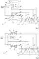
- the figure 1 is a schematic partial sectional view of an electronic chip 1 of a first type comprising N-type doped semiconductor wells 3 formed in the upper part of a P-type doped semiconductor substrate 5 For the sake of clarity, only one box and part of another box are shown in figure 1 .
- N-channel MOS transistors 6 are formed in and on the portions of the substrate between wells 3 and include gates 7 and drain and source areas 9 and 11.
- P-channel MOS transistors 12 are formed in and on. the wells 3 and include gates 13 and drain and source areas 15 and 17.
- the transistors are coupled together to compose circuits, for example circuits digital.
- an inverter logic circuit between nodes 19 and 21 is shown.
- the digital circuits include supply nodes 23 and 25. In the example shown, supply nodes 23 and 25 are respectively coupled to sources 11 and 17 of transistors 6 and 12.
- the N-type doped wells 3, or N wells, are provided with bias contacts 27 and the substrate is provided with bias contacts 29.
- the transistors and the bias contacts are separated by isolation trenches 31.
- a reference potential GND for example ground, is applied both to the supply nodes 23 and to the bias contacts 29 of the P wells.
- a supply circuit not shown included in the chip, provides an applied potential VDD. both on the power supply nodes 25 and on the polarization contacts 27 of the N boxes.
- the figure 2 is a schematic partial sectional view of an electronic chip 40 of a second type comprising N wells 3 and P wells 33 extending over an N-type doped buried layer 42 covering a P-type doped substrate 5.
- the wells 3 and 33 correspond to the wells 3 and 33 of the chip 1 described above, that is to say they comprise bias contacts 27 and 29 and digital circuits made up of transistors 6, 12 formed in and on the caissons.
- the digital circuits are provided with power supply nodes 23 and 25.
- the digital circuits are supplied between ground GND and a potential VDD applied respectively to the nodes 23 and 25.
- Polarization potentials VPW and VNW which may not be identical to the potentials GND and VDD, are applied respectively to the polarization contacts 29 and 27, and are provided by supply circuits not shown included in the chip.
- the figure 3 shows an embodiment of an electronic chip 50 of the first type protected against attacks.
- the figure 3 comprises a partial sectional view of the chip 50 and a representation of circuits included in this chip.
- the chip 50 comprises elements of the chip 1 described in relation to the figure 1 and in particular N 3 wells and P wells 33.
- Circuits for example digital circuits, include transistors 6 formed in and on P wells 33 and transistors 12 formed in and on N wells 3.
- Digital circuits have supply nodes 23 and 25 and wells 3 and 33 are provided with respective polarization contacts 27 and 29. The polarization contacts and the transistors are separated by isolation trenches 31.
- the power supply nodes 23 of the circuits are coupled to ground.
- the chip 50 comprises a supply circuit 52 (VDD) which supplies a potential VDD applied to the supply nodes 25.
- VDD supply circuit 52
- the supply circuit 52 is itself supplied between a positive potential VCC and a potential of GND ground supplied by a power source (not shown) external to the chip 50.
- the bias contacts 29 of the P wells are not connected directly to ground, but are coupled to ground by a resistive element 54 included in the chip.
- the voltage at the terminals of the resistive element 54 is compared with a threshold by a comparator circuit 56 adapted to produce an alert signal AP when this voltage is greater than the threshold.
- the resistive element 54 and the comparator circuit 56 constitute thus a circuit 57 for detecting the bias current of the wells 33.
- the polarization contacts 27 of the N wells are coupled to the supply circuit 52 by a resistive element 58.
- the voltage across the terminals of the resistive element 58 is compared to a threshold by a comparator circuit 60 adapted to produce a warning signal. AN when this voltage is greater than the threshold.
- the resistive element 58 and the comparator circuit 60 thus constitute a circuit 61 for detecting the bias current of the wells 3.
- the junctions between the N wells and the substrate are reverse biased, and no significant bias current flows in the resistive elements 54 and 58.
- the aforementioned thresholds can therefore be very low.
- chip 1 is advantageously protected against any attack by fault injection, regardless of the location of the attack on the surface of the chip.
- resistors 54 and 58 can be between 1 and 100 ⁇ .
- the resistive elements 54 and 58 can be components or portions of the chip, for example portions of wells, adapted to produce a voltage when a current flows.
- the figure 4 shows an embodiment of an electronic chip 70 of the second type protected against attacks.
- the figure 4 schematically comprises a view in partial section of the chip 70 and a representation of circuits included in this chip.
- the chip 70 comprises elements of the chip 40 described in relation to the figure 2 and in particular N wells 3 and P wells 33 extending over an N-type doped buried layer 42 covering a P-type doped substrate 5.
- Circuits for example digital circuits, formed in and on the wells, have power supply nodes 23 and 25.
- the N 3 wells are provided with polarization contacts 27 and the P wells 33 are provided with polarization contacts 29.
- the power supply nodes 23 of the digital circuits are coupled to ground.
- the chip 70 includes a power supply circuit 52 which supplies a potential VDD applied to the power nodes 25.
- the bias contacts 29 of the P wells are coupled to a power supply circuit 72 which produces a potential VPW.
- the power supply circuit 72 comprises a detection circuit 73 (DETP) of the bias current supplied to the P wells.
- the detection circuit 73 is adapted to produce an AP signal when the bias current is greater, in absolute value, than a threshold.
- the bias contacts 27 of the N wells are coupled to a power supply circuit 74 which produces a bias potential VNW.
- the power supply circuit 74 comprises a detection circuit 75 (DETN) of the bias current supplied to the N wells.
- the detection circuit 75 is adapted to produce a signal AN when the bias current is greater, in absolute value, than a threshold.
- the supply circuits 52, 72 and 74 are supplied between potentials VCC and GND supplied by a supply device, not shown, external to the chip.
- the detection by the chip 70 is similar to the detection by the chip 50 of the figure 3 .
- the bias currents I1 detected by the chip are separated from the supply currents I2 for the normal activity of the chip.
- the bias potentials VNW and VPW can be different from the supply potentials VDD and GND, for example to accelerate the operation of the chip, or else to reduce its consumption.
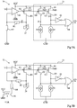
- the figure 5A details an embodiment of a power supply circuit 74 coupled to a bias contact 27 of an N well.
- the power supply circuit 74 comprises an operational amplifier 80 whose output is coupled to the gate G1 of a transistor P-channel MOS type PM1.
- Two resistors R1 and R2 connected in series couple drain D1 of transistor PM1 to ground, the common node between the resistors being coupled to the positive input of amplifier 80.
- a regulated potential V0 is applied to the negative input of amplifier 80.
- Amplifier 80 is supplied between ground GND and a node for applying a potential VCC supplied by an external power supply device.
- the source S1 of the transistor PM1 is coupled to the potential VCC.
- the bias contacts 27 are coupled to the drain D1.
- the detection circuit 75 of the power supply circuit 74 comprises two P-channel MOS type transistors PM2 and PM3, forming current mirrors with the transistor PM1, that is to say whose gates G2 and G3 are coupled with the gate G1 and the sources D2 and D3 are coupled to the source S1.
- Drain D2 of transistor PM2 is coupled to ground by a source of current which draws a current I3 + on the drain D2.
- Drain D3 of transistor PM3 is coupled to ground by a current source which draws a current I3- from drain D3, current I3- being less than current I3 +.
- An inverter 82 couples the drain D3 to an input of an OR gate 84 whose other input is coupled to the drain D2. Activation of the output of gate 84 produces signal AN.
- a current I3 flows through the resistors R1 and R2, the current I3 being chosen to be between the currents I3 + and I3-. This current is added to the bias current I1 in the transistor PM1, and a current I5 equal to I1 + I3 flows in each of the transistors PM2 and PM3.
- the current I5 is between the currents I3- and I3 +, and the AN output is deactivated.
- the detection circuit 75 locates this variation in potential to detect the current I1.
- the detection circuit 75 can be replaced by any circuit suitable for detecting a variation of a regulation potential of a supply circuit.
- the difference between the currents I3 and 13- corresponds to the detection threshold of a current I1 coming from the polarization contact 27 and the difference between the currents I3 and I3 + corresponds to the detection threshold of a current I1 flowing to the polarization contact. 27.
- the detection thresholds are between 0.2 and 2 mA.
- the figure 5B details an embodiment of a power supply circuit 72 coupled to a bias contact 29 of an N well.
- the supply circuit 72 corresponds to the supply circuit 74 of the figure 5A , in which the resistors R1 and R2 have been replaced by resistors R3 and R4 in series coupling the drain D1 to a supply circuit 86, the common node between the resistors R3 and R4 being coupled to the positive input of the amplifier 80.
- the detection circuits 73 and 75 are similar.
- the power supply circuit 86 produces a potential lower than the ground potential, from the positive potential VCC and from the ground.
- Circuit 86 may be a clock synchronized charge pump (CLK) circuit.
- the detection circuit 73 can be replaced by a detection circuit suitable for detecting a variation of a regulation potential of the circuit 86.
- the secure chips include digital circuits comprising MOS transistors 6 and 12
- identically protected chips may also include analog circuits, for example comprising components such as bipolar transistors. , resistors or diodes, the important thing being that the chip has polarized wells.
- a P-type doped substrate 5 has been provided, variations are possible in which the substrate 5 is replaced by an N-type doped substrate or by an N-type doped substrate. Silicon-on-insulator type, or by a support in another semiconductor.
- each of the detection circuits 73 and 75 of the embodiment of a secure chip of the second type can replace one or the other of the detection circuits 57 and 61 of the embodiment of a secure chip of the first type. type.
Landscapes
- Engineering & Computer Science (AREA)
- Physics & Mathematics (AREA)
- Computer Security & Cryptography (AREA)
- Theoretical Computer Science (AREA)
- Nonlinear Science (AREA)
- Computer Hardware Design (AREA)
- General Physics & Mathematics (AREA)
- General Engineering & Computer Science (AREA)
- Computer Networks & Wireless Communication (AREA)
- Signal Processing (AREA)
- Software Systems (AREA)
- Microelectronics & Electronic Packaging (AREA)
- Semiconductor Integrated Circuits (AREA)
Description
- La présente demande concerne les puces électroniques, en particulier des puces électroniques sécurisées contre des attaques.
- Des puces électroniques contenant des informations confidentielles, telles que des puces de cartes bancaires, sont susceptibles de subir des attaques de pirates visant à déterminer le fonctionnement de la puce et à en extraire les informations confidentielles. Une attaque peut être effectuée sur la puce en fonctionnement connectée entre les bornes d'une source d'alimentation. Une façon de réaliser une telle attaque consiste pour un pirate à balayer la surface de la puce avec un faisceau laser qui perturbe par impulsions le fonctionnement de la puce. C'est l'observation des conséquences de ces perturbations, parfois appelées fautes, sur l'activité du circuit, qui permet au pirate de mener à bien son attaque. Pour perturber le fonctionnement de la puce, le pirate peut aussi réaliser des contacts sur la surface de la puce et y appliquer des potentiels. Le pirate peut aussi disposer une bobine près de la surface de la puce afin d'émettre des perturbations électromagnétiques.
- Il est souhaitable de disposer de puces électroniques protégées contre ce type d'attaque, dit attaque par injection de fautes, les dispositifs connus présentant divers inconvénients et difficultés de mise en oeuvre.
- Les documents
FR 2981783 FR 2986683 - Ainsi, un mode de réalisation prévoit une puce électronique sécurisée comprenant une pluralité de caissons semiconducteurs polarisés et un circuit de détection du courant de polarisation des caissons.
- Selon un mode de réalisation, le circuit de détection est adapté à produire un signal d'alerte lorsque le courant de polarisation est supérieur, en valeur absolue, à un seuil.
- Selon un mode de réalisation, le circuit de détection comprend un élément résistif parcouru par le courant de polarisation, le circuit de détection étant adapté à détecter une tension aux bornes de l'élément résistif.
- Selon un mode de réalisation, l'élément résistif a une résistance comprise entre 1 et 100 Ω.
- Selon un mode de réalisation, la puce électronique sécurisée comprend un circuit d'alimentation adapté à fournir un potentiel de polarisation desdits caissons, le circuit de détection étant adapté à détecter une variation d'un potentiel régulant le potentiel de polarisation.
- Selon un mode de réalisation, le circuit d'alimentation comprend un amplificateur opérationnel dont la sortie est couplée à la grille d'un premier transistor MOS, et le circuit de détection comprend un deuxième transistor MOS formant un miroir de courant avec le premier transistor MOS, une entrée de l'amplificateur opérationnel et le drain du premier transistor MOS étant couplés auxdits caissons, et le circuit de détection étant adapté à détecter une variation du courant dans le deuxième transistor.
- Selon un mode de réalisation, la pluralité de caissons comprend des premiers caissons d'un premier type de conductivité et des deuxièmes caissons d'un deuxième type de conductivité, le circuit de détection comprenant d'une part un premier circuit détectant le courant de polarisation des premiers caissons et d'autre part un second circuit détectant le courant de polarisation des deuxièmes caissons.
- Selon un mode de réalisation, les premiers caissons sont formés dans la partie supérieure d'un substrat semiconducteur du deuxième type de conductivité et les deuxièmes caissons sont des parties supérieures du substrat comprises entre les premiers caissons.
- Selon un mode de réalisation, les premiers caissons et les deuxièmes caissons s'étendent sur une couche enterrée dopée du premier type de conductivité recouvrant un substrat du deuxième type de conductivité.
- Un autre mode de réalisation prévoit un procédé de sécurisation d'une puce électronique comportant une pluralité de caissons semiconducteurs polarisés, comprenant une étape de détection du courant de polarisation des caissons.
- Selon un mode de réalisation, la puce contient des données confidentielles, le procédé comprenant, quand le courant de polarisation détecté est supérieur à un seuil, une étape de destruction des données confidentielles.
- Selon un mode de réalisation, le procédé comprend, quand le courant de polarisation détecté est supérieur à un seuil, une étape d'arrêt de l'activité de la puce.
- Ces caractéristiques et avantages, ainsi que d'autres, seront exposés en détail dans la description suivante de modes de réalisation particuliers faite à titre non limitatif en relation avec les figures jointes parmi lesquelles :
- la
figure 1 est une vue en coupe partielle schématique d'une puce électronique d'un premier type ; - la
figure 2 est une vue en coupe partielle schématique d'une puce électronique d'un deuxième type ; - la
figure 3 représente un mode de réalisation d'une puce électronique du premier type protégée contre des attaques ; - la
figure 4 représente un mode de réalisation d'une puce électronique du deuxième type protégée contre des attaques ; et - les
figures 5A et 5B détaillent des modes de réalisation de circuits d'alimentation et de détection. - De mêmes éléments ont été désignés par de mêmes références aux différentes figures et, de plus, les diverses figures ne sont pas tracées à l'échelle. Par souci de clarté, seuls les éléments qui sont utiles à la compréhension des modes de réalisation décrits ont été représentés et sont détaillés.
- Dans la description qui suit, lorsque l'on fait référence à des qualificatifs de position relative, tels que le terme "supérieur", il est fait référence à l'orientation de l'élément concerné dans les figures.
- Dans la présente description, le terme "connecté" désigne une connexion électrique directe entre deux éléments, tandis que le terme "couplé" désigne une connexion électrique entre deux éléments qui peut être directe ou par l'intermédiaire d'un ou de plusieurs autres composants passifs ou actifs, comme des résistances, des condensateurs, des inductances, des diodes, des transistors, etc.
- La
figure 1 est une vue en coupe partielle schématique d'une puce électronique 1 d'un premier type comprenant des caissons semiconducteurs 3 dopés de type N formés dans la partie supérieure d'un substrat semiconducteur 5 dopé de type P. Par souci de clarté, seuls un caisson et une partie d'un autre caisson sont représentés enfigure 1 . - Des transistors MOS à canal N 6 sont formés dans et sur les parties du substrat situées entre les caissons 3 et comprennent des grilles 7 et des zones de drain et de source 9 et 11. Des transistors MOS à canal P 12 sont formés dans et sur les caissons 3 et comprennent des grilles 13 et des zones de drain et de source 15 et 17. Les transistors sont couplés entre eux pour composer des circuits, par exemple des circuits numériques. A titre d'exemple illustratif, un circuit logique inverseur entre des noeuds 19 et 21 est représenté. Les circuits numériques comprennent des noeuds d'alimentation 23 et 25. Dans l'exemple représenté, les noeuds d'alimentation 23 et 25 sont couplés respectivement aux sources 11 et 17 des transistors 6 et 12.
- Les caissons 3 dopés de type N, ou caissons N, sont munis de contacts de polarisation 27 et le substrat est muni de contacts de polarisation 29. Les transistors et les contacts de polarisation sont séparés par des tranchées d'isolement 31.
- Un potentiel de référence GND, par exemple la masse, est appliqué à la fois sur les noeuds d'alimentation 23 et sur les contacts de polarisation 29 des caissons P. Un circuit d'alimentation non représenté compris dans la puce fournit un potentiel VDD appliqué à la fois sur les noeuds d'alimentation 25 et sur les contacts de polarisation 27 des caissons N.
- Dans la suite de la description, dans une puce électronique du premier type, on appellera caisson P les parties supérieures 33 du substrat comprises entre des caissons N.
- La
figure 2 est une vue en coupe partielle schématique d'une puce électronique 40 d'un deuxième type comprenant des caissons N 3 et des caissons P 33 s'étendant sur une couche enterrée 42 dopée de type N recouvrant un substrat 5 dopé de type P. - Les caissons 3 et 33 correspondent aux caissons 3 et 33 de la puce 1 décrite précédemment c'est-à-dire qu'ils comportent des contacts de polarisation 27 et 29 et des circuits numériques composés par des transistors 6, 12 formés dans et sur les caissons. Les circuits numériques sont munis de noeuds d'alimentation 23 et 25.
- Les circuits numériques sont alimentés entre la masse GND et un potentiel VDD appliqués respectivement sur les noeuds 23 et 25. Des potentiels de polarisation VPW et VNW, pouvant ne pas être identiques aux potentiels GND et VDD, sont appliqués respectivement sur les contacts de polarisation 29 et 27, et sont fournis par des circuits d'alimentation non représentés compris dans la puce.
- Comme on l'a indiqué en préambule, pour des circuits contenant des informations confidentielles, un pirate est susceptible de procéder à une analyse par injection de fautes. Des modes de détection de telles attaques sont décrits ci-après.
- La
figure 3 représente un mode de réalisation d'une puce électronique 50 du premier type protégée contre des attaques. Lafigure 3 comprend une vue en coupe partielle de la puce 50 et une représentation de circuits compris dans cette puce. - La puce 50 comprend des éléments de la puce 1 décrite en relation avec la
figure 1 et notamment des caissons N 3 et des caissons P 33. Des circuits, par exemple des circuits numériques, comprennent des transistors 6 formés dans et sur les caissons P 33 et des transistors 12 formés dans et sur les caissons N 3. Les circuits numériques ont des noeuds d'alimentation 23 et 25 et les caissons 3 et 33 sont munis de contacts de polarisation respectifs 27 et 29. Les contacts de polarisation et les transistors sont séparés par des tranchées d'isolement 31. - Les noeuds d'alimentation 23 des circuits sont couplés à la masse. De plus, la puce 50 comprend un circuit d'alimentation 52 (VDD) qui fournit un potentiel VDD appliqué sur les noeuds d'alimentation 25. Le circuit d'alimentation 52 est lui-même alimenté entre un potentiel VCC positif et un potentiel de masse GND fournis par une source d'alimentation non représentée externe à la puce 50.
- Les contacts de polarisation 29 des caissons P ne sont pas connectés directement à la masse, mais sont couplés à la masse par un élément résistif 54 compris dans la puce. La tension aux bornes de l'élément résistif 54 est comparée à un seuil par un circuit comparateur 56 adapté à produire un signal d'alerte AP lorsque cette tension est supérieure au seuil. L'élément résistif 54 et le circuit comparateur 56 constituent ainsi un circuit de détection 57 du courant de polarisation des caissons 33.
- Les contacts de polarisation 27 des caissons N sont couplés au circuit d'alimentation 52 par un élément résistif 58. La tension aux bornes de l'élément résistif 58 est comparée à un seuil par un circuit comparateur 60 adapté à produire un signal d'alerte AN lorsque cette tension est supérieure au seuil. L'élément résistif 58 et le circuit comparateur 60 constituent ainsi un circuit de détection 61 du courant de polarisation des caissons 3.
- En fonctionnement normal, les jonctions entre les caissons N et le substrat sont polarisées en inverse, et aucun courant de polarisation notable ne circule dans les éléments résistifs 54 et 58. Les seuils susmentionnés peuvent donc être très faibles.
- Lors d'une tentative d'attaque de la puce par injection de fautes, par exemple au moment où un pirate bombarde la puce par un faisceau laser, des courants I1N et I1P apparaissent entre les contacts de polarisation 27 des caissons N 3 et les contacts de polarisation 29 des caissons P 33. Ces courants de polarisation I1N et I1P sont détectés par les circuits de détection 57 ou 61 et provoquent l'émission de signaux d'alerte AN ou AP. Le signal est utilisé par la puce pour prendre des contre-mesures comme suspendre ou arrêter son activité ou détruire des informations confidentielles qu'elle contient.
- Lors d'une tentative d'attaque par un pirate, les courants I1P et I1N qui résultent d'une perturbation du fonctionnement de la puce sont analysés par la puce pour détecter l'attaque. Les courants de polarisation I1N et I1P utilisés pour détecter l'attaque correspondent directement aux courants résultant de la perturbation. Ainsi, la puce détecte une énergie injectée très inférieure à l'énergie minimale d'injection de faute. De ce fait, la puce 1 est avantageusement protégée contre toute attaque par injection de fautes, quelle que soit la localisation de l'attaque sur la surface de la puce.
- A titre d'exemple, les résistances 54 et 58 peuvent être comprises entre 1 et 100 Ω. A titre de variante, les éléments résistifs 54 et 58 peuvent être des composants ou des portions de la puce, par exemple des portions de caissons, adaptés à produire une tension au passage d'un courant.
- La
figure 4 représente un mode de réalisation d'une puce électronique 70 du deuxième type protégée contre des attaques. Lafigure 4 comprend, de manière schématique, une vue en coupe partielle de la puce 70 et une représentation de circuits compris dans cette puce. - La puce 70 comprend des éléments de la puce 40 décrite en relation avec la
figure 2 et notamment des caissons N 3 et des caissons P 33 s'étendant sur une couche enterrée 42 dopée de type N recouvrant un substrat 5 dopé de type P. Des circuits, par exemple des circuits numériques, formés dans et sur les caissons, ont des noeuds d'alimentation 23 et 25. Les caissons N 3 sont munis de contacts de polarisation 27 et les caissons P 33 sont munis de contacts de polarisation 29. - Les noeuds d'alimentation 23 des circuits numériques sont couplés à la masse. De plus, la puce 70 comprend un circuit d'alimentation 52 qui fournit un potentiel VDD appliqué sur les noeuds d'alimentation 25.
- Les contacts de polarisation 29 des caissons P sont couplés à un circuit d'alimentation 72 qui produit un potentiel VPW. Le circuit d'alimentation 72 comprend un circuit de détection 73 (DETP) du courant de polarisation fourni aux caissons P. Le circuit de détection 73 est adapté à produire un signal AP lorsque le courant de polarisation est supérieur, en valeur absolue, à un seuil.
- Les contacts de polarisation 27 des caissons N sont couplés à un circuit d'alimentation 74 qui produit un potentiel de polarisation VNW. Le circuit d'alimentation 74 comprend un circuit de détection 75 (DETN) du courant de polarisation fourni aux caissons N. Le circuit de détection 75 est adapté à produire un signal AN lorsque le courant de polarisation est supérieur, en valeur absolue, à un seuil.
- Les circuits d'alimentation 52, 72 et 74 sont alimentés entre des potentiels VCC et GND fournis par un dispositif d'alimentation, non représenté, extérieur à la puce.
- En cas d'attaque par injection de fautes, la détection par la puce 70 est similaire à la détection par la puce 50 de la
figure 3 . Les courants de polarisation I1 détectés par la puce sont séparés des courants I2 d'alimentation de l'activité normale de la puce. Dans le mode de réalisation de la puce 70, les potentiels de polarisation VNW et VPW peuvent être différents des potentiels d'alimentation VDD et GND, par exemple pour accélérer le fonctionnement de la puce, ou bien pour diminuer sa consommation. - La
figure 5A détaille un mode de réalisation d'un circuit d'alimentation 74 couplé à un contact 27 de polarisation d'un caisson N. Le circuit d'alimentation 74 comprend un amplificateur opérationnel 80 dont la sortie est couplée à la grille G1 d'un transistor PM1 de type MOS à canal P. Deux résistances R1 et R2 connectées en série couplent le drain D1 du transistor PM1 à la masse, le noeud commun entre les résistances étant couplé à l'entrée positive de l'amplificateur 80. Un potentiel régulé V0 est appliqué sur l'entrée négative de l'amplificateur 80. L'amplificateur 80 est alimenté entre la masse GND et un noeud d'application d'un potentiel VCC fourni par un dispositif extérieur d'alimentation. La source S1 du transistor PM1 est couplée au potentiel VCC. Les contacts de polarisation 27 sont couplés au drain D1. - Le circuit de détection 75 du circuit d'alimentation 74 comprend deux transistors PM2 et PM3 de type MOS à canal P, formant des miroirs de courant avec le transistor PM1, c'est-à-dire dont les grilles G2 et G3 sont couplées avec la grille G1 et les sources D2 et D3 sont couplées à la source S1. Le drain D2 du transistor PM2 est couplé à la masse par une source de courant qui prélève un courant I3+ sur le drain D2. Le drain D3 du transistor PM3 est couplé à la masse par une source de courant qui prélève un courant I3- sur le drain D3, le courant I3- étant inférieur au courant I3+. Un inverseur 82 couple le drain D3 à une entrée d'une porte OU 84 dont l'autre entrée est couplée au drain D2. L'activation de la sortie de la porte 84 produit le signal AN.
- Lorsque le circuit 74 fonctionne, un courant I3 circule dans les résistances R1 et R2, le courant I3 étant choisi pour être compris entre les courants I3+ et I3-. Ce courant s'ajoute au courant de polarisation I1 dans le transistor PM1, et un courant I5 égal à I1 + I3 circule dans chacun des transistors PM2 et PM3.
- En fonctionnement normal, le courant I5 est compris entre les courants I3- et I3+, et la sortie AN est désactivée.
- En cas de tentative d'attaque, dès que le courant I5 sort de l'intervalle compris entre 13- et I3+, le potentiel du drain D2 augmente ou le potentiel du drain D3 diminue, et la sortie AN est activée. Autrement dit, l'apparition d'un courant I1 provoque une variation du potentiel fourni par l'amplificateur 80 qui régule la tension fournie par le circuit d'alimentation 74, et le circuit de détection 75 repère cette variation de potentiel pour détecter le courant I1. A titre de variante, le circuit de détection 75 peut être remplacé par tout circuit adapté à détecter une variation d'un potentiel de régulation d'un circuit d'alimentation.
- La différence entre les courants I3 et 13- correspond au seuil de détection d'un courant I1 provenant du contact de polarisation 27 et la différence entre les courants I3 et I3+ correspond au seuil de détection d'un courant I1 circulant vers le contact de polarisation 27. A titre d'exemple, les seuils de détection sont compris entre 0,2 et 2 mA.
- La
figure 5B détaille un mode de réalisation d'un circuit d'alimentation 72 couplé à un contact 29 de polarisation d'un caisson N. - Le circuit d'alimentation 72 correspond au circuit d'alimentation 74 de la
figure 5A , dans lequel les résistances R1 et R2 ont été remplacées par des résistances R3 et R4 en série couplant le drain D1 à un circuit d'alimentation 86, le noeud commun entre les résistances R3 et R4 étant couplé à l'entrée positive de l'amplificateur 80. A titre d'exemple, les circuits de détection 73 et 75 sont similaires. - Le circuit d'alimentation 86 produit un potentiel inférieur au potentiel de la masse, à partir du potentiel positif VCC et de la masse. Le circuit 86 peut être un circuit à pompe de charge synchronisé par une horloge (CLK) . A titre de variante, le circuit de détection 73 peut être remplacé par un circuit de détection adapté à repérer une variation d'un potentiel de régulation du circuit 86.
- Des modes de réalisation particuliers ont été décrits. Diverses variantes et modifications apparaîtront à l'homme de l'art. En particulier, bien que dans les modes de réalisation décrits, les courants de polarisation des caissons P 33 et les courants de polarisation des caissons N 3 soient surveillés simultanément par deux circuits de détection, des variantes sont possibles dans lesquelles le courant de polarisation des caissons d'un seul type de conductivité est surveillé par un seul circuit de détection.
- En outre, bien que dans les modes de réalisation décrits, les puces sécurisées comportent des circuits numériques comprenant des transistors MOS 6 et 12, des puces protégées de manière identique peuvent aussi comporter des circuits analogiques, par exemple comprenant des composants tels que des transistors bipolaires, des résistances ou des diodes, l'important étant que la puce comporte des caissons polarisés.
- De plus, bien que, dans les modes de réalisation décrits, un substrat 5 dopé de type P ait été prévu, des variantes sont possibles dans lesquelles le substrat 5 est remplacé par un substrat dopé de type N ou par un support de type silicium sur isolant, ou encore par un support en un autre semiconducteur.
- En outre, bien que des circuits de détection particuliers aient été détaillés dans les modes de réalisation décrits, d'autres circuits de détection adaptés à détecter un courant de polarisation sont possibles.
- Divers modes de réalisation avec diverses variantes ont été décrits ci-dessus. On notera que l'homme de l'art pourra combiner divers éléments de ces divers modes de réalisation et variantes sans faire preuve d'activité inventive. En particulier, chacun des circuits de détection 73 et 75 du mode de réalisation d'une puce sécurisée du deuxième type peut remplacer l'un ou l'autre des circuits de détection 57 et 61 du mode de réalisation d'une puce sécurisée du premier type.
- De plus, des modes de réalisation adaptés à des puces de circuits intégrés d'un premier type et d'un deuxième type ont été décrits. Ce qui a été décrit s'applique bien évidemment à d'autres types de technologie de circuit intégré, comprenant divers types de caissons.
Claims (7)
- Puce électronique sécurisée (50 ; 70) comprenant dans un substrat (5) une pluralité de caissons semiconducteurs (3, 33) polarisés dopés de type N ou P et un circuit de détection (57, 61 ; 73, 75) du courant de polarisation des caissons, des transistors (6, 12) étant formés dans et sur les caissons, le circuit de détection (57, 61) étant :relié aux caissons ;ourelié à des contacts de polarisation (29) de parties (33) du substrat dans et sur lesquelles sont formés des transistors (6),le circuit de détection (57, 61) étant caractérisé en ce qu'il comprend un élément résistif parcouru par le courant de polarisation, le circuit de détection étant adapté à détecter une tension aux bornes de l'élément résistif,la puce électronique comprenant un circuit d'alimentation (72, 74) adapté à fournir un potentiel de polarisation desdits caissons (3, 33), le circuit de détection (73, 75) étant adapté à détecter une variation d'un potentiel régulant le potentiel de polarisation,le circuit d'alimentation (72, 74) comprend un amplificateur opérationnel (80) dont la sortie est couplée à la grille d'un premier transistor MOS (PM1), etle circuit de détection (73, 75) comprend un deuxième transistor MOS (PM2) formant un miroir de courant avec le premier transistor MOS, une entrée de l'amplificateur opérationnel et le drain du premier transistor MOS étant couplés auxdits caissons (3, 33), et le circuit de détection étant adapté à détecter une variation du courant dans le deuxième transistor.
- Puce électronique selon la revendication 1, dans laquelle le circuit de détection (57, 61 ; 73, 75) est adapté à produire un signal d'alerte (AN, AP) lorsque le courant de polarisation est supérieur, en valeur absolue, à un seuil.
- Puce électronique selon la revendication 1 ou 2, dans laquelle l'élément résistif (54, 58) a une résistance comprise entre 1 et 100 Ω.
- Puce électronique (50 ; 70) selon l'une quelconque des revendications 1 à 3, dans laquelle la pluralité de caissons comprend des premiers caissons d'un premier type de conductivité et des deuxièmes caissons d'un deuxième type de conductivité, le circuit de détection comprenant d'une part un premier circuit détectant le courant de polarisation des premiers caissons et d'autre part un second circuit détectant le courant de polarisation des deuxièmes caissons.
- Puce électronique (50) selon la revendication 4, dans laquelle les premiers caissons sont formés dans la partie supérieure d'un substrat semiconducteur (5) du deuxième type de conductivité et les deuxièmes caissons sont des parties supérieures du substrat comprises entre les premiers caissons.
- Puce électronique (70) selon la revendication 4, dans laquelle les premiers caissons et les deuxièmes caissons s'étendent sur une couche enterrée (42) dopée du premier type de conductivité recouvrant un substrat (5) du deuxième type de conductivité.
- Procédé de sécurisation d'une puce électronique selon l'une quelconque des revendications 1 à 6, comprenant, quand le courant de polarisation détecté est supérieur à un seuil, une étape de destruction de données confidentielles ou une étape d'arrêt de l'activité de la puce.
Applications Claiming Priority (1)
| Application Number | Priority Date | Filing Date | Title |
|---|---|---|---|
| FR1560089A FR3042891B1 (fr) | 2015-10-22 | 2015-10-22 | Puce electronique securisee |
Publications (2)
| Publication Number | Publication Date |
|---|---|
| EP3159872A1 EP3159872A1 (fr) | 2017-04-26 |
| EP3159872B1 true EP3159872B1 (fr) | 2021-08-11 |
Family
ID=55361629
Family Applications (1)
| Application Number | Title | Priority Date | Filing Date |
|---|---|---|---|
| EP16161366.6A Active EP3159872B1 (fr) | 2015-10-22 | 2016-03-21 | Puce électronique sécurisée au moyen de multiple caissons |
Country Status (4)
| Country | Link |
|---|---|
| US (1) | US10691840B2 (fr) |
| EP (1) | EP3159872B1 (fr) |
| CN (3) | CN106611209B (fr) |
| FR (1) | FR3042891B1 (fr) |
Families Citing this family (10)
| Publication number | Priority date | Publication date | Assignee | Title |
|---|---|---|---|---|
| FR3042891B1 (fr) * | 2015-10-22 | 2018-03-23 | Stmicroelectronics (Rousset) Sas | Puce electronique securisee |
| FR3050317A1 (fr) | 2016-04-19 | 2017-10-20 | Stmicroelectronics Rousset | Puce electronique |
| FR3062952B1 (fr) | 2017-02-13 | 2019-03-29 | Stmicroelectronics (Crolles 2) Sas | Condensateur de decouplage |
| FR3070092A1 (fr) * | 2017-08-11 | 2019-02-15 | Stmicroelectronics (Rousset) Sas | Protection d'un circuit integre |
| DE102017120944B4 (de) * | 2017-09-11 | 2020-10-01 | Infineon Technologies Ag | Chip mit Schaltung zum Detektieren eines Angriffs auf den Chip |
| FR3072211B1 (fr) | 2017-10-11 | 2021-12-10 | St Microelectronics Rousset | Procede de detection d'une injection de fautes et d'un amincissement du substrat dans un circuit integre, et circuit integre associe |
| US10306753B1 (en) | 2018-02-22 | 2019-05-28 | International Business Machines Corporation | Enclosure-to-board interface with tamper-detect circuit(s) |
| US11122682B2 (en) | 2018-04-04 | 2021-09-14 | International Business Machines Corporation | Tamper-respondent sensors with liquid crystal polymer layers |
| FR3081240B1 (fr) | 2018-05-15 | 2021-08-06 | St Microelectronics Rousset | Puce electronique |
| FR3083919A1 (fr) * | 2018-07-13 | 2020-01-17 | Stmicroelectronics (Rousset) Sas | Puce electronique protegee |
Family Cites Families (7)
| Publication number | Priority date | Publication date | Assignee | Title |
|---|---|---|---|---|
| US6864539B2 (en) * | 2002-07-19 | 2005-03-08 | Semiconductor Technology Academic Research Center | Semiconductor integrated circuit device having body biasing circuit for generating forward well bias voltage of suitable level by using simple circuitry |
| DE60320314T2 (de) * | 2003-02-20 | 2009-06-25 | International Business Machines Corp. | Testverfahren für integrierte schaltungen mit verwendung modifikation von well-spannungen |
| US7847581B2 (en) * | 2008-04-03 | 2010-12-07 | Stmicroelectronics (Rousset) Sas | Device for protecting an integrated circuit against a laser attack |
| FR2981783B1 (fr) * | 2011-10-19 | 2014-05-09 | St Microelectronics Rousset | Systeme de detection d'une attaque par laser d'une puce de circuit integre |
| FR2986633B1 (fr) * | 2012-02-08 | 2014-09-05 | St Microelectronics Rousset | Dispositif de detection d'une attaque par laser dans une puce de circuit integre |
| CN103383736A (zh) | 2012-05-02 | 2013-11-06 | 中频电子股份有限公司 | 对电子芯片进行验证的方法与使用者终端 |
| FR3042891B1 (fr) * | 2015-10-22 | 2018-03-23 | Stmicroelectronics (Rousset) Sas | Puce electronique securisee |
-
2015
- 2015-10-22 FR FR1560089A patent/FR3042891B1/fr not_active Expired - Fee Related
-
2016
- 2016-03-21 EP EP16161366.6A patent/EP3159872B1/fr active Active
- 2016-04-25 CN CN201610352606.0A patent/CN106611209B/zh active Active
- 2016-04-25 CN CN202010608733.9A patent/CN111783920B/zh active Active
- 2016-04-25 US US15/137,789 patent/US10691840B2/en active Active
- 2016-04-25 CN CN201620482834.5U patent/CN205621041U/zh not_active Expired - Lifetime
Non-Patent Citations (1)
| Title |
|---|
| None * |
Also Published As
| Publication number | Publication date |
|---|---|
| EP3159872A1 (fr) | 2017-04-26 |
| CN111783920B (zh) | 2025-05-13 |
| CN106611209A (zh) | 2017-05-03 |
| US20170116439A1 (en) | 2017-04-27 |
| CN205621041U (zh) | 2016-10-05 |
| CN111783920A (zh) | 2020-10-16 |
| US10691840B2 (en) | 2020-06-23 |
| CN106611209B (zh) | 2020-08-11 |
| FR3042891A1 (fr) | 2017-04-28 |
| FR3042891B1 (fr) | 2018-03-23 |
Similar Documents
| Publication | Publication Date | Title |
|---|---|---|
| EP3159872A1 (fr) | Puce électronique sécurisée au moyen de de multiple caissons | |
| EP0551038B1 (fr) | Protection générale d'un circuit intégré contre les surcharges permanentes et décharges électrostatiques | |
| EP2535932B1 (fr) | Puce de circuit intégré comprenant un dispositif de protection contre des attaques | |
| FR2752335A1 (fr) | Circuit integre incorporant un circuit pour piloter des transistors de puissance montes selon une configuration en demi-pont permettant une oscillation negative excessive du noeud de sortie | |
| EP2369622B1 (fr) | Procédé et dispositif de contremesure contre une attaque par injection d'erreur dans un microcircuit électronique | |
| EP3301605B1 (fr) | Puce électronique protégée | |
| EP3236496B1 (fr) | Puce électronique protégée contre des attaques en face arrière | |
| EP2109139A2 (fr) | Dispositif de protection d'un circuit intégré contre une attaque par laser | |
| FR2981783A1 (fr) | Systeme de detection d'une attaque par laser d'une puce de circuit integre | |
| EP2535933B1 (fr) | Puce de circuit intégré comprenant un dispositif de protection contre des attaques | |
| WO2017203187A1 (fr) | Circuit intégré comprenant une pluralité de puces formées d'un transistor à haute tension et comprenant une puce formée d'un transistor à basse tension | |
| EP3151277B1 (fr) | Circuit intégré sécurisé | |
| EP3217547A1 (fr) | Inverseur a trois etats, bascule d a verrouillage et bistable maitre-esclave comprenant des tfet | |
| FR3112004A1 (fr) | Détection d'une impulsion électromagnétique | |
| EP3770789B1 (fr) | Procédé de protection de données stockées dans une mémoire, et circuit intégré correspondant | |
| FR2875328A1 (fr) | Cellule memoire sram protegee contre des pics de courant ou de tension | |
| EP3483773B1 (fr) | Procédé de modification aléatoire du profil de consommation d'un circuit logique, et dispositif associé | |
| EP3525236B1 (fr) | Procédé de détection d'une atteinte à l'intégrité d'un substrat semi-conducteur d'un circuit intégré depuis sa face arrière, et dispositif correspondant | |
| FR2884988A1 (fr) | Bascule protegee contre les pics de courant ou de tension | |
| EP3583699B1 (fr) | Circuit de polarisation active et faible consommation d'une entrée haute impédance | |
| EP3593380A1 (fr) | Puce electronique | |
| FR2958078A1 (fr) | Procede et dispositif de contremesure contre une attaque par injection d'erreur dans un microcircuit electronique | |
| EP3594999B1 (fr) | Puce électronique protégée | |
| FR3058564A1 (fr) | Procede et circuit de polarisation de circuits integres | |
| FR3063597A1 (fr) | Architecture de puce electronique |
Legal Events
| Date | Code | Title | Description |
|---|---|---|---|
| PUAI | Public reference made under article 153(3) epc to a published international application that has entered the european phase |
Free format text: ORIGINAL CODE: 0009012 |
|
| STAA | Information on the status of an ep patent application or granted ep patent |
Free format text: STATUS: REQUEST FOR EXAMINATION WAS MADE |
|
| 17P | Request for examination filed |
Effective date: 20160321 |
|
| AK | Designated contracting states |
Kind code of ref document: A1 Designated state(s): AL AT BE BG CH CY CZ DE DK EE ES FI FR GB GR HR HU IE IS IT LI LT LU LV MC MK MT NL NO PL PT RO RS SE SI SK SM TR |
|
| AX | Request for extension of the european patent |
Extension state: BA ME |
|
| STAA | Information on the status of an ep patent application or granted ep patent |
Free format text: STATUS: EXAMINATION IS IN PROGRESS |
|
| 17Q | First examination report despatched |
Effective date: 20190613 |
|
| GRAP | Despatch of communication of intention to grant a patent |
Free format text: ORIGINAL CODE: EPIDOSNIGR1 |
|
| STAA | Information on the status of an ep patent application or granted ep patent |
Free format text: STATUS: GRANT OF PATENT IS INTENDED |
|
| INTG | Intention to grant announced |
Effective date: 20201216 |
|
| GRAJ | Information related to disapproval of communication of intention to grant by the applicant or resumption of examination proceedings by the epo deleted |
Free format text: ORIGINAL CODE: EPIDOSDIGR1 |
|
| STAA | Information on the status of an ep patent application or granted ep patent |
Free format text: STATUS: EXAMINATION IS IN PROGRESS |
|
| GRAP | Despatch of communication of intention to grant a patent |
Free format text: ORIGINAL CODE: EPIDOSNIGR1 |
|
| STAA | Information on the status of an ep patent application or granted ep patent |
Free format text: STATUS: GRANT OF PATENT IS INTENDED |
|
| INTC | Intention to grant announced (deleted) | ||
| INTG | Intention to grant announced |
Effective date: 20210412 |
|
| GRAS | Grant fee paid |
Free format text: ORIGINAL CODE: EPIDOSNIGR3 |
|
| GRAA | (expected) grant |
Free format text: ORIGINAL CODE: 0009210 |
|
| STAA | Information on the status of an ep patent application or granted ep patent |
Free format text: STATUS: THE PATENT HAS BEEN GRANTED |
|
| AK | Designated contracting states |
Kind code of ref document: B1 Designated state(s): AL AT BE BG CH CY CZ DE DK EE ES FI FR GB GR HR HU IE IS IT LI LT LU LV MC MK MT NL NO PL PT RO RS SE SI SK SM TR |
|
| REG | Reference to a national code |
Ref country code: CH Ref legal event code: EP |
|
| REG | Reference to a national code |
Ref country code: DE Ref legal event code: R096 Ref document number: 602016061876 Country of ref document: DE |
|
| REG | Reference to a national code |
Ref country code: IE Ref legal event code: FG4D Free format text: LANGUAGE OF EP DOCUMENT: FRENCH Ref country code: AT Ref legal event code: REF Ref document number: 1420191 Country of ref document: AT Kind code of ref document: T Effective date: 20210915 |
|
| REG | Reference to a national code |
Ref country code: LT Ref legal event code: MG9D |
|
| REG | Reference to a national code |
Ref country code: NL Ref legal event code: MP Effective date: 20210811 |
|
| REG | Reference to a national code |
Ref country code: AT Ref legal event code: MK05 Ref document number: 1420191 Country of ref document: AT Kind code of ref document: T Effective date: 20210811 |
|
| PG25 | Lapsed in a contracting state [announced via postgrant information from national office to epo] |
Ref country code: ES Free format text: LAPSE BECAUSE OF FAILURE TO SUBMIT A TRANSLATION OF THE DESCRIPTION OR TO PAY THE FEE WITHIN THE PRESCRIBED TIME-LIMIT Effective date: 20210811 Ref country code: FI Free format text: LAPSE BECAUSE OF FAILURE TO SUBMIT A TRANSLATION OF THE DESCRIPTION OR TO PAY THE FEE WITHIN THE PRESCRIBED TIME-LIMIT Effective date: 20210811 Ref country code: PT Free format text: LAPSE BECAUSE OF FAILURE TO SUBMIT A TRANSLATION OF THE DESCRIPTION OR TO PAY THE FEE WITHIN THE PRESCRIBED TIME-LIMIT Effective date: 20211213 Ref country code: NO Free format text: LAPSE BECAUSE OF FAILURE TO SUBMIT A TRANSLATION OF THE DESCRIPTION OR TO PAY THE FEE WITHIN THE PRESCRIBED TIME-LIMIT Effective date: 20211111 Ref country code: AT Free format text: LAPSE BECAUSE OF FAILURE TO SUBMIT A TRANSLATION OF THE DESCRIPTION OR TO PAY THE FEE WITHIN THE PRESCRIBED TIME-LIMIT Effective date: 20210811 Ref country code: BG Free format text: LAPSE BECAUSE OF FAILURE TO SUBMIT A TRANSLATION OF THE DESCRIPTION OR TO PAY THE FEE WITHIN THE PRESCRIBED TIME-LIMIT Effective date: 20211111 Ref country code: LT Free format text: LAPSE BECAUSE OF FAILURE TO SUBMIT A TRANSLATION OF THE DESCRIPTION OR TO PAY THE FEE WITHIN THE PRESCRIBED TIME-LIMIT Effective date: 20210811 Ref country code: SE Free format text: LAPSE BECAUSE OF FAILURE TO SUBMIT A TRANSLATION OF THE DESCRIPTION OR TO PAY THE FEE WITHIN THE PRESCRIBED TIME-LIMIT Effective date: 20210811 Ref country code: RS Free format text: LAPSE BECAUSE OF FAILURE TO SUBMIT A TRANSLATION OF THE DESCRIPTION OR TO PAY THE FEE WITHIN THE PRESCRIBED TIME-LIMIT Effective date: 20210811 Ref country code: HR Free format text: LAPSE BECAUSE OF FAILURE TO SUBMIT A TRANSLATION OF THE DESCRIPTION OR TO PAY THE FEE WITHIN THE PRESCRIBED TIME-LIMIT Effective date: 20210811 |
|
| PG25 | Lapsed in a contracting state [announced via postgrant information from national office to epo] |
Ref country code: PL Free format text: LAPSE BECAUSE OF FAILURE TO SUBMIT A TRANSLATION OF THE DESCRIPTION OR TO PAY THE FEE WITHIN THE PRESCRIBED TIME-LIMIT Effective date: 20210811 Ref country code: LV Free format text: LAPSE BECAUSE OF FAILURE TO SUBMIT A TRANSLATION OF THE DESCRIPTION OR TO PAY THE FEE WITHIN THE PRESCRIBED TIME-LIMIT Effective date: 20210811 Ref country code: GR Free format text: LAPSE BECAUSE OF FAILURE TO SUBMIT A TRANSLATION OF THE DESCRIPTION OR TO PAY THE FEE WITHIN THE PRESCRIBED TIME-LIMIT Effective date: 20211112 |
|
| PG25 | Lapsed in a contracting state [announced via postgrant information from national office to epo] |
Ref country code: NL Free format text: LAPSE BECAUSE OF FAILURE TO SUBMIT A TRANSLATION OF THE DESCRIPTION OR TO PAY THE FEE WITHIN THE PRESCRIBED TIME-LIMIT Effective date: 20210811 |
|
| PG25 | Lapsed in a contracting state [announced via postgrant information from national office to epo] |
Ref country code: DK Free format text: LAPSE BECAUSE OF FAILURE TO SUBMIT A TRANSLATION OF THE DESCRIPTION OR TO PAY THE FEE WITHIN THE PRESCRIBED TIME-LIMIT Effective date: 20210811 |
|
| REG | Reference to a national code |
Ref country code: DE Ref legal event code: R097 Ref document number: 602016061876 Country of ref document: DE |
|
| PG25 | Lapsed in a contracting state [announced via postgrant information from national office to epo] |
Ref country code: SM Free format text: LAPSE BECAUSE OF FAILURE TO SUBMIT A TRANSLATION OF THE DESCRIPTION OR TO PAY THE FEE WITHIN THE PRESCRIBED TIME-LIMIT Effective date: 20210811 Ref country code: SK Free format text: LAPSE BECAUSE OF FAILURE TO SUBMIT A TRANSLATION OF THE DESCRIPTION OR TO PAY THE FEE WITHIN THE PRESCRIBED TIME-LIMIT Effective date: 20210811 Ref country code: RO Free format text: LAPSE BECAUSE OF FAILURE TO SUBMIT A TRANSLATION OF THE DESCRIPTION OR TO PAY THE FEE WITHIN THE PRESCRIBED TIME-LIMIT Effective date: 20210811 Ref country code: EE Free format text: LAPSE BECAUSE OF FAILURE TO SUBMIT A TRANSLATION OF THE DESCRIPTION OR TO PAY THE FEE WITHIN THE PRESCRIBED TIME-LIMIT Effective date: 20210811 Ref country code: CZ Free format text: LAPSE BECAUSE OF FAILURE TO SUBMIT A TRANSLATION OF THE DESCRIPTION OR TO PAY THE FEE WITHIN THE PRESCRIBED TIME-LIMIT Effective date: 20210811 Ref country code: AL Free format text: LAPSE BECAUSE OF FAILURE TO SUBMIT A TRANSLATION OF THE DESCRIPTION OR TO PAY THE FEE WITHIN THE PRESCRIBED TIME-LIMIT Effective date: 20210811 |
|
| PLBE | No opposition filed within time limit |
Free format text: ORIGINAL CODE: 0009261 |
|
| STAA | Information on the status of an ep patent application or granted ep patent |
Free format text: STATUS: NO OPPOSITION FILED WITHIN TIME LIMIT |
|
| 26N | No opposition filed |
Effective date: 20220512 |
|
| PG25 | Lapsed in a contracting state [announced via postgrant information from national office to epo] |
Ref country code: IT Free format text: LAPSE BECAUSE OF FAILURE TO SUBMIT A TRANSLATION OF THE DESCRIPTION OR TO PAY THE FEE WITHIN THE PRESCRIBED TIME-LIMIT Effective date: 20210811 |
|
| PG25 | Lapsed in a contracting state [announced via postgrant information from national office to epo] |
Ref country code: SI Free format text: LAPSE BECAUSE OF FAILURE TO SUBMIT A TRANSLATION OF THE DESCRIPTION OR TO PAY THE FEE WITHIN THE PRESCRIBED TIME-LIMIT Effective date: 20210811 |
|
| PG25 | Lapsed in a contracting state [announced via postgrant information from national office to epo] |
Ref country code: MC Free format text: LAPSE BECAUSE OF FAILURE TO SUBMIT A TRANSLATION OF THE DESCRIPTION OR TO PAY THE FEE WITHIN THE PRESCRIBED TIME-LIMIT Effective date: 20210811 |
|
| REG | Reference to a national code |
Ref country code: CH Ref legal event code: PL |
|
| GBPC | Gb: european patent ceased through non-payment of renewal fee |
Effective date: 20220321 |
|
| REG | Reference to a national code |
Ref country code: BE Ref legal event code: MM Effective date: 20220331 |
|
| PG25 | Lapsed in a contracting state [announced via postgrant information from national office to epo] |
Ref country code: LU Free format text: LAPSE BECAUSE OF NON-PAYMENT OF DUE FEES Effective date: 20220321 Ref country code: LI Free format text: LAPSE BECAUSE OF NON-PAYMENT OF DUE FEES Effective date: 20220331 Ref country code: IE Free format text: LAPSE BECAUSE OF NON-PAYMENT OF DUE FEES Effective date: 20220321 Ref country code: GB Free format text: LAPSE BECAUSE OF NON-PAYMENT OF DUE FEES Effective date: 20220321 Ref country code: FR Free format text: LAPSE BECAUSE OF NON-PAYMENT OF DUE FEES Effective date: 20220331 Ref country code: CH Free format text: LAPSE BECAUSE OF NON-PAYMENT OF DUE FEES Effective date: 20220331 |
|
| PG25 | Lapsed in a contracting state [announced via postgrant information from national office to epo] |
Ref country code: BE Free format text: LAPSE BECAUSE OF NON-PAYMENT OF DUE FEES Effective date: 20220331 |
|
| PG25 | Lapsed in a contracting state [announced via postgrant information from national office to epo] |
Ref country code: HU Free format text: LAPSE BECAUSE OF FAILURE TO SUBMIT A TRANSLATION OF THE DESCRIPTION OR TO PAY THE FEE WITHIN THE PRESCRIBED TIME-LIMIT; INVALID AB INITIO Effective date: 20160321 |
|
| PG25 | Lapsed in a contracting state [announced via postgrant information from national office to epo] |
Ref country code: MK Free format text: LAPSE BECAUSE OF FAILURE TO SUBMIT A TRANSLATION OF THE DESCRIPTION OR TO PAY THE FEE WITHIN THE PRESCRIBED TIME-LIMIT Effective date: 20210811 Ref country code: CY Free format text: LAPSE BECAUSE OF FAILURE TO SUBMIT A TRANSLATION OF THE DESCRIPTION OR TO PAY THE FEE WITHIN THE PRESCRIBED TIME-LIMIT Effective date: 20210811 |
|
| PG25 | Lapsed in a contracting state [announced via postgrant information from national office to epo] |
Ref country code: TR Free format text: LAPSE BECAUSE OF FAILURE TO SUBMIT A TRANSLATION OF THE DESCRIPTION OR TO PAY THE FEE WITHIN THE PRESCRIBED TIME-LIMIT Effective date: 20210811 |
|
| PG25 | Lapsed in a contracting state [announced via postgrant information from national office to epo] |
Ref country code: MT Free format text: LAPSE BECAUSE OF FAILURE TO SUBMIT A TRANSLATION OF THE DESCRIPTION OR TO PAY THE FEE WITHIN THE PRESCRIBED TIME-LIMIT Effective date: 20210811 |
|
| PGFP | Annual fee paid to national office [announced via postgrant information from national office to epo] |
Ref country code: DE Payment date: 20260219 Year of fee payment: 11 |