EP3158609B1 - Modulationsmuster für oberflächenstreuungsantennen - Google Patents
Modulationsmuster für oberflächenstreuungsantennen Download PDFInfo
- Publication number
- EP3158609B1 EP3158609B1 EP15808884.9A EP15808884A EP3158609B1 EP 3158609 B1 EP3158609 B1 EP 3158609B1 EP 15808884 A EP15808884 A EP 15808884A EP 3158609 B1 EP3158609 B1 EP 3158609B1
- Authority
- EP
- European Patent Office
- Prior art keywords
- antenna
- wave
- scattering
- scattering elements
- discrete
- Prior art date
- Legal status (The legal status is an assumption and is not a legal conclusion. Google has not performed a legal analysis and makes no representation as to the accuracy of the status listed.)
- Active
Links
Images



Classifications
-
- H—ELECTRICITY
- H01—ELECTRIC ELEMENTS
- H01Q—ANTENNAS, i.e. RADIO AERIALS
- H01Q3/00—Arrangements for changing or varying the orientation or the shape of the directional pattern of the waves radiated from an antenna or antenna system
- H01Q3/44—Arrangements for changing or varying the orientation or the shape of the directional pattern of the waves radiated from an antenna or antenna system varying the electric or magnetic characteristics of reflecting, refracting, or diffracting devices associated with the radiating element
-
- H—ELECTRICITY
- H01—ELECTRIC ELEMENTS
- H01Q—ANTENNAS, i.e. RADIO AERIALS
- H01Q13/00—Waveguide horns or mouths; Slot antennas; Leaky-waveguide antennas; Equivalent structures causing radiation along the transmission path of a guided wave
- H01Q13/20—Non-resonant leaky-waveguide or transmission-line antennas; Equivalent structures causing radiation along the transmission path of a guided wave
-
- H—ELECTRICITY
- H01—ELECTRIC ELEMENTS
- H01Q—ANTENNAS, i.e. RADIO AERIALS
- H01Q11/00—Electrically-long antennas having dimensions more than twice the shortest operating wavelength and consisting of conductive active radiating elements
- H01Q11/02—Non-resonant antennas, e.g. travelling-wave antenna
Definitions
- ERA Electronically Reconfigurable Aperture
- V A Manasson et al. discloses a new electronically beam-steering technology that is compatible with highly integrated antenna design and dramatically simplifies packaging.
- WO 2012/050614 discloses surface scattering antennas which provide adjustable radiation fields by adjustably coupling scattering elements along a wave-propagating structure.
- Surface wave control using nonperiodic parasitic strips in printed antennas by R G Rojas et al. disclose a scheme for controlling the surface wave behaviour on printed planar antennas.
- the wavy line 105 is a symbolic depiction of the guided wave or surface wave, and this symbolic depiction is not intended to indicate an actual wavelength or amplitude of the guided wave or surface wave; moreover, while the wavy line 105 is depicted as within the wave-propagating structure 104 (e.g. as for a guided wave in a metallic waveguide), for a surface wave the wave may be substantially localized outside the wave-propagating structure (e.g. as for a TM mode on a single wire transmission line or a "spoof plasmon" on an artificial impedance surface).
- the wave-propagating structure 104 e.g. as for a guided wave in a metallic waveguide
- the wave may be substantially localized outside the wave-propagating structure (e.g. as for a TM mode on a single wire transmission line or a "spoof plasmon" on an artificial impedance surface).
- inventions may provide a plurality of feed connectors attached to the wave-propagating structure at a plurality of locations (peripheral and/or non-peripheral).
- the scattering elements 102a , 102b are adjustable scattering elements having electromagnetic properties that are adjustable in response to one or more external inputs.
- adjustable scattering elements can include elements that are adjustable in response to voltage inputs (e.g. bias voltages for active elements (such as varactors, transistors, diodes) or for elements that incorporate tunable dielectric materials (such as ferroelectrics or liquid crystals)), current inputs (e.g. direct injection of charge carriers into active elements), optical inputs (e.g. illumination of a photoactive material), field inputs (e.g.
- the scattering elements 102a , 102b have first and second couplings to the guided wave or surface wave 105 that are functions of the first and second electromagnetic properties, respectively.
- the first and second couplings may be first and second polarizabilities of the scattering elements at the frequency or frequency band of the guided wave or surface wave.
- the first coupling is a substantially nonzero coupling whereas the second coupling is a substantially zero coupling.
- both couplings are substantially nonzero but the first coupling is substantially greater than (or less than) than the second coupling.
- the first and second scattering elements 102a , 102b are responsive to the guided wave or surface wave 105 to produce a plurality of scattered electromagnetic waves having amplitudes that are functions of (e.g. are proportional to) the respective first and second couplings.
- a superposition of the scattered electromagnetic waves comprises an electromagnetic wave that is depicted, in this example, as a plane wave 110 that radiates from the surface scattering antenna 100 .
- the guided wave or surface wave may be represented by a complex scalar input wave ⁇ in that is a function of position along the wave-propagating structure 104 , and it is desired that the surface scattering antenna produce an output wave that may be represented by another complex scalar wave ⁇ out .
- a pattern of adjustment of the scattering elements may be selected that corresponds to an interference pattern of the input and output waves along the wave-propagating structure.
- the scattering elements may be adjusted to provide couplings to the guided wave or surface wave that are functions of (e.g. are proportional to, or step-functions of) an interference term given by Re ⁇ out ⁇ in ⁇ .
- embodiments of the surface scattering antenna may be adjusted to provide arbitrary antenna radiation patterns by identifying an output wave ⁇ out corresponding to a selected beam pattern, and then adjusting the scattering elements accordingly as above.
- Embodiments of the surface scattering antenna may therefore be adjusted to provide, for example, a selected beam direction (e.g. beam steering), a selected beam width or shape (e.g. a fan or pencil beam having a broad or narrow beamwidth), a selected arrangement of nulls (e.g. null steering), a selected arrangement of multiple beams, a selected polarization state (e.g. linear, circular, or elliptical polarization), a selected overall phase, or any combination thereof.
- embodiments of the surface scattering antenna may be adjusted to provide a selected near field radiation profile, e.g. to provide near-field focusing and/or near-field nulls.
- the scattering elements may be arranged along the wave-propagating structure with inter-element spacings that are much less than a free-space wavelength corresponding to an operating frequency of the device (for example, less than one-third, one-fourth, or one-fifth of this free-space wavelength).
- the operating frequency is a microwave frequency, selected from frequency bands such as L, S, C, X, Ku, K, Ka, Q, U, V, E, W, F, and D, corresponding to frequencies ranging from about 1 GHz to 170 GHz and free-space wavelengths ranging from millimeters to tens of centimeters.
- the operating frequency is an RF frequency, for example in the range of about 100 MHz to 1 GHz.
- the operating frequency is a millimeter-wave frequency, for example in the range of about 170 GHz to 300 GHz.
- the surface scattering antenna includes a substantially one-dimensional wave-propagating structure 104 having a substantially one-dimensional arrangement of scattering elements, and the pattern of adjustment of this one-dimensional arrangement may provide, for example, a selected antenna radiation profile as a function of zenith angle (i.e. relative to a zenith direction that is parallel to the one-dimensional wave-propagating structure).
- the surface scattering antenna includes a substantially two-dimensional wave-propagating structure 104 having a substantially two-dimensional arrangement of scattering elements, and the pattern of adjustment of this two-dimensional arrangement may provide, for example, a selected antenna radiation profile as a function of both zenith and azimuth angles (i.e.
- FIGS. 2A - 4B Exemplary adjustment patterns and beam patterns for a surface scattering antenna that includes a two-dimensional array of scattering elements distributed on a planar rectangular wave-propagating structure are depicted in FIGS. 2A - 4B .
- the planar rectangular wave-propagating structure includes a monopole antenna feed that is positioned at the geometric center of the structure.
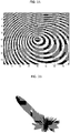
- FIG. 2A presents an adjustment pattern that corresponds to a narrow beam having a selected zenith and azimuth as depicted by the beam pattern diagram of FIG. 2B .
- the wave-propagating structure is a modular wave-propagating structure and a plurality of modular wave-propagating structures may be assembled to compose a modular surface scattering antenna.
- a plurality of substantially one-dimensional wave-propagating structures may be arranged, for example, in an interdigital fashion to produce an effective two-dimensional arrangement of scattering elements.
- the interdigital arrangement may comprise, for example, a series of adjacent linear structures (i.e. a set of parallel straight lines) or a series of adjacent curved structures (i.e. a set of successively offset curves such as sinusoids) that substantially fills a two-dimensional surface area.
- These interdigital arrangements may include a feed connector having a tree structure , e.g.
- a binary tree providing repeated forks that distribute energy from the feed structure 108 to the plurality of linear structures (or the reverse thereof).
- a plurality of substantially two-dimensional wave-propagating structures (each of which may itself comprise a series of one-dimensional structures, as above) may be assembled to produce a larger aperture having a larger number of scattering elements; and/or the plurality of substantially two-dimensional wave-propagating structures may be assembled as a three-dimensional structure (e.g. forming an A-frame structure, a pyramidal structure, or other multi-faceted structure).
- each of the plurality of modular wave-propagating structures may have its own feed connector(s) 106 , and/or the modular wave-propagating structures may be configured to couple a guided wave or surface wave of a first modular wave-propagating structure into a guided wave or surface wave of a second modular wave-propagating structure by virtue of a connection between the two structures.
- the number of modules to be assembled may be selected to achieve an aperture size providing a desired telecommunications data capacity and/or quality of service, and/or a three-dimensional arrangement of the modules may be selected to reduce potential scan loss.
- the modular assembly could comprise several modules mounted at various locations/orientations flush to the surface of a vehicle such as an aircraft, spacecraft, watercraft, ground vehicle, etc. (the modules need not be contiguous).
- the wave-propagating structure may have a substantially non-linear or substantially non-planar shape whereby to conform to a particular geometry, therefore providing a conformal surface scattering antenna (conforming, for example, to the curved surface of a vehicle).
- a surface scattering antenna is a reconfigurable antenna that may be reconfigured by selecting a pattern of adjustment of the scattering elements so that a corresponding scattering of the guided wave or surface wave produces a desired output wave.
- the surface scattering antenna includes a plurality of scattering elements distributed at positions ⁇ r j , ⁇ along a wave-propagating structure 104 as in FIG. 1 (or along multiple wave-propagating structures, for a modular embodiment) and having a respective plurality of adjustable couplings ⁇ ⁇ j ⁇ to the guided wave or surface wave 105 .
- the guided wave or surface wave 105 presents a wave amplitude A j and phase ⁇ j to the j th scattering element; subsequently, an output wave is generated as a superposition of waves scattered from the plurality of scattering elements:
- E ( ⁇ , ⁇ ) represents the electric field component of the output wave on a far-field radiation sphere
- R j ( ⁇ , ⁇ ) represents a (normalized) electric field pattern for the scattered wave that is generated by the j th scattering element in response to an excitation caused by the coupling ⁇ j
- k ( ⁇ , ⁇ ) represents a wave vector of magnitude ⁇ / c that is perpendicular to the radiation sphere at ( ⁇ , ⁇ ) .
- embodiments of the surface scattering antenna may provide a reconfigurable antenna that is adjustable to produce a desired output wave E ( ⁇ , ⁇ ) by
- These propagation characteristics may include, for example, an effective refractive index and/or an effective wave impedance, and these effective electromagnetic properties may be at least partially determined by the arrangement and adjustment of the scattering elements along the wave-propagating structure.
- the reconfigurable antenna is adjustable to provide a desired polarization state of the output wave E ( ⁇ , ⁇ ).
- first and second subsets LP (1) and LP (2) of the scattering elements provide (normalized) electric field patterns R (1) ( ⁇ , ⁇ ) and R (2) ( ⁇ , ⁇ ), respectively, that are substantially linearly polarized and substantially orthogonal (for example, the first and second subjects may be scattering elements that are perpendicularly oriented on a surface of the wave-propagating structure 104 ).
- any desired polarization e.g. linear, circular, or elliptical
- a desired output wave E ( ⁇ , ⁇ ) may be controlled by adjusting gains of individual amplifiers for the plurality of feeds. Adjusting a gain for a particular feed line would correspond to multiplying the A j ' s by a gain factor G for those elements j that are fed by the particular feed line.
- depolarization loss e.g., as a beam is scanned off-broadside
- depolarization loss may be compensated by adjusting the relative gain(s) between the first feed(s) and the second feed(s).
- the ideal complex continuous hologram function is approximated by an actual modulation function defined on a discrete-valued domain (for the discrete positions of the scattering elements) and having a discrete-valued range (for the discrete available tunable settings of the scattering elements).
- a square wave contains an (infinite) series of higher harmonics.
- the antenna may be designed so that the higher harmonics correspond to evanescent waves, making them non-radiating, but their aliases do still map into non-evanescent waves and radiate as grating lobes.
- FIGS. 5A-5F An illustrative example of the discretization and aliasing effect is shown in FIGS. 5A-5F.
- FIG. 5A depicts a continuous hologram function that is a simple sinusoid 500 ; in Fourier space, this is represented as a single Fourier mode 510 as shown in FIG. 5D .
- the Heaviside function is applied to the sinusoid, the result is a square wave 502 as shown in FIG. 5B ; in Fourier space, the square wave includes the fundamental Fourier mode 510 and an (infinite) series of higher harmonics 511 , 512 , 513 , etc. as shown in FIG. 5E .
- one of the harmonics ( 513 ) is aliased into the non-evanescent spatial frequency range ( 523 ) and can radiate as a grating lobe.
- the first harmonic 511 is unaliased but also within the non-evanescent spatial frequency range, so it can generate another undesirable side lobe
- the Heaviside function is not the only choice for a binary hologram, and other choices may eliminate, average, or otherwise mitigate the higher harmonics and the resulting side/grating lobes.
- a useful way to view these approaches is as attempting to "smooth" or "blur" the sharp corners in the Heaviside without resorting to values other than 0 and 1.
- the single step of the Heaviside function may be replaced by a function that resembles a pulse-width-modulated (PWM) square wave with a duty cycle that gradually increases from 0 to 1 over the range of the sinusoid.
- PWM pulse-width-modulated
- a probabilistic or dithering approach may be used to determine the settings of the individual scattering elements, for example by randomly adjusting each scattering element to the "on” or “off” state according to a probability that gradually increases from 0 to 1 over the range of the sinusoid.
- the binary approximation of the hologram may be improved by increasing the density of scattering elements.
- An increased density results in a larger number of adjustable parameters that can be optimized, and a denser array results in better homogenization of electromagnetic parameters.
- the binary approximation of the hologram may be improved by arranging the elements in a non-uniform spatial pattern. If the scattering elements are placed on non-uniform grid, the rigid periodicity of the Heaviside modulation is broken, which spreads out the higher harmonics.
- the non-uniform spatial pattern can be a random distribution, e.g. with a selected standard deviation and mean, and/or it can be a gradient distribution, with a density of scattering elements that varies with position along the wave-propagating structure. For example, the density may be larger near the center of the aperture to realize an amplitude envelope.
- the binary approximation of the hologram may be improved using error propagation or error diffusion techniques to determine the modulation pattern.
- An error propagation technique may involve considering the desired value of a pure sinusoid modulation and tracking a cumulative difference between that and the Heaviside (or other discretization function). The error accumulates, and when it reaches a threshold it carries over to the current cell.
- the error propagation may be performed independently on each row; or the error propagation may be performed row-by-row by carrying over an error tally from the end of row to the beginning of the next row; or the error propagation may be performed multiple times along different directions (e.g.
- the error propagation may use a two-dimensional error propagation kernel as with Floyd-Steinberg or Jarvis-Judice-Ninke error diffusion.
- the rows for error diffusion can correspond to individual one-dimensional waveguides, or the rows for error diffusion can be oriented perpendicularly to the one-dimensional waveguides.
- the rows can be defined with respect to the waveguide mode, e.g. by defining the rows as a series of successive phase fronts of the waveguide mode (thus, a center-fed parallel plate waveguide would have "rows" that are concentric circles around the feed point).
- undesirable grating lobes can be reduced by flipping individual bits corresponding to individual scattering elements.
- each element can be described as a single bit which contributes spectrally to both the desired fundamental modulation and to the higher harmonics that give rise to grating lobes.
- single bits that contribute to harmonics more than the fundamental can be flipped, reducing the total harmonics level while leaving the fundamental relatively unaffected.
- Undesirable grating lobes can be reduced by "chopping" the range-discretized hologram (e.g. after applying the Heaviside function but before sampling at the discrete set of scattering element locations) to selectively reduce or eliminate higher harmonics.
- Selective elimination of square wave harmonics is described, for example, in H. S. Patel and R.G. Hoft, "Generalized Techniques of Harmonic Elimination and Voltage Control in Thyristor Inverters: Part I-Harmonic Elimination," IEEE Trans. Ind. App. Vol. IA-9, 310 (1973 ).
- the square wave 502 of FIG. 5B can be modified with "chops" that eliminate the harmonics 511 and 513 (as shown in FIG. 5E ) so that neither the harmonic 511 nor the aliased harmonic 531 (as shown in FIG. 5F ) will generate grating lobes.
- Undesirable grating lobes may be reduced by adjusting the wavevector of the modulation pattern. Adjusting the wavevector of the modulation pattern shifts the primary beam, but shifts grating lobes coming from aliased beams to a greater degree (due to the additional 2 ⁇ phase shift on every alias). Adjustment of the phase and wavevector of the applied modulation pattern can be used to intentionally form constructive and destructive interference of the grating lobes, side lobes, and main beam. Thus, allowing very minor changes in the angle and phase of the main radiated beam can grant a large parameter space in which to optimize/minimize grating lobes.
- the antenna modulation pattern can be selected according to an optimization algorithm that optimizes a particular cost function.
- the modulation pattern may be calculated to optimize: realized gain (maximum total intensity in the main beam); relative minimization of the highest side lobe or grating lobe relative to main beam; minimization of main-beam FWHM (beam width); or maximization of main-beam directivity (height above all integrated side lobes and grating lobes); or any combination thereof (e.g. by using a collective cost function that is a weighted sum of individual cost functions, or by selecting a Pareto optimum of individual cost functions).
- the optimization can be either global (searching the entire space of antenna configurations to optimize the cost function) or local (starting from an initial guess and applying an optimization algorithm to find a local extremum of the cost function).
- optimization algorithms may be utilized to perform the optimization of the desired cost function.
- the optimization may proceed using discrete optimization variables corresponding to the discrete adjustment states of the scattering elements, or the optimization may proceed using continuous optimization variables that can be mapped to the discrete adjustment states by a smoothed step function (e.g. a smoothed Heaviside function for a binary antenna or a smoothed sequential stair-step function for a grayscale antenna).
- a smoothed step function e.g. a smoothed Heaviside function for a binary antenna or a smoothed sequential stair-step function for a grayscale antenna.
- Other optimization approaches can include optimization with a genetic optimization algorithm or a simulated annealing optimization algorithm.
- the optimization algorithm can involve an iterative process that includes identifying a trial antenna configuration, calculating a gradient of the cost function for the antenna configuration, and then selecting a subsequent trial configuration, repeating the process until some termination condition is met.
- the gradient can be calculated by, for example, calculating finite-difference estimates of the partial derivatives of the cost function with respect to the individual optimization variables. For N scattering elements, this might involve performing N full-wave simulations, or performing N measurements of a test antenna in a test environment (e.g. an anechoic chamber).
- the gradient may be calculable by an adjoint sensitivity method that entails solving a single adjoint problem instead of N finite-difference problems; adjoint sensitivity models are available in conventional numerical software packages such as HFSS or CST Microwave Studio.
- adjoint sensitivity models are available in conventional numerical software packages such as HFSS or CST Microwave Studio.
- a subsequent trial configuration can be calculated using various optimization iteration approaches such as quasi-Newton methods or conjugate gradient methods.
- the iterative process may terminate, for example, when the norm of the cost function gradient becomes sufficiently small, or when the cost function reaches a satisfactory minimum (or maximum).
- the optimization can be performed on a reduced set of modulation patterns.
- N or g N , for g grayscale levels
- the optimization may be constrained to consider only those modulation patterns that yield a desired primary spectral content in the output wave ⁇ out , and/or the optimization may be constrained to consider only those modulation patterns which have a spatial on-off fraction within a known range relevant for the design.
- a signal bearing medium examples include, but are not limited to, the following: a recordable type medium such as a floppy disk, a hard disk drive, a Compact Disc (CD), a Digital Video Disk (DVD), a digital tape, a computer memory, etc.; and a transmission type medium such as a digital and/or an analog communication medium (e.g., a fiber optic cable, a waveguide, a wired communications link, a wireless communication link, etc.).
- electrical circuitry includes, but is not limited to, electrical circuitry having at least one discrete electrical circuit, electrical circuitry having at least one integrated circuit, electrical circuitry having at least one application specific integrated circuit, electrical circuitry forming a general purpose computing device configured by a computer program (e.g., a general purpose computer configured by a computer program which at least partially carries out processes and/or devices described herein, or a microprocessor configured by a computer program which at least partially carries out processes and/or devices described herein), electrical circuitry forming a memory device (e.g., forms of random access memory), and/or electrical circuitry forming a communications device (e.g., a modem, communications switch, or optical-electrical equipment).
- a computer program e.g., a general purpose computer configured by a computer program which at least partially carries out processes and/or devices described herein, or a microprocessor configured by a computer program which at least partially carries out processes and/or devices described herein
- electrical circuitry forming a memory device
Landscapes
- Variable-Direction Aerials And Aerial Arrays (AREA)
- Aerials With Secondary Devices (AREA)
Claims (7)
- Verfahren, umfassend:Diskretisieren einer Hologrammfunktion für eine Oberflächenstreuungsantenne (100) durch:Identifizieren von mehreren diskreten Orten auf einer Apertur der Oberflächenstreuungsantenne für mehrere diskrete Streuungselemente der Oberflächenstreuungsantenne, undIdentifizieren des diskreten Satzes von Zuständen für jedes der Streuungselemente entsprechend einem diskreten Satz von Hologrammfunktionswerten bei jedem der Orte der Streuungselemente; undIdentifizieren einer Antennenkonfiguration, die dem Diskretisieren der Hologrammfunktion zuzuschreibende Artefakte reduziert, wobei die Antennenkonfiguration den mehreren diskreten Orten auf der Apertur und dem diskreten Satz von Zuständen für jedes der Streuungselemente entspricht,dadurch gekennzeichnet, dassdas Identifizieren der Antennenkonfiguration das Abändern der Hologrammfunktion durch Ersetzen einer fundamentalen räumlichen Fourier-Komponente der Hologrammfunktion durch mehrere räumliche Fourier-Komponenten beinhaltet.
- Verfahren nach Anspruch 1, weiter umfassend:
Verstellen der Oberflächenstreuungsantenne zu der identifizierten Antennenkonfiguration. - Verfahren nach Anspruch 1, weiter umfassend:
Speichern der identifizierten Antennenkonfiguration in einem Speichermedium. - System, umfassend:eine Oberflächenstreuungsantenne (100; 600) mit mehreren entlang einer Wellenausbreitungsstruktur (104) verteilten verstellbaren Streuungselementen (102, 102b);ein Speichermedium (620), auf das ein Satz von Antennenkonfigurationen entsprechend einem Satz von Hologrammfunktionen beschrieben ist, wobei jede Antennenkonfiguration ausgewählt wird zum Reduzieren von einer Diskretisierung der jeweiligen Hologrammfunktion zuzuschreibenden Artefakten; undeine Steuerschaltungsanordnung (610), betreibbar zum Lesen von Antennenkonfigurationen aus dem Ablagemedium und Verstellen der mehreren verstellbaren Streuungselemente, um die Antennenkonfigurationen bereitzustellen,wobei die Oberflächenstreuungsantenne eine Apertur definiert und die Steuerschaltungsanordnung konfiguriert ist zumIdentifizieren von mehreren diskreten Orten auf der Apertur für mehrere diskrete Streuungselemente der Oberflächenstreuungsantenne, undIdentifizieren eines diskreten Satzes von Zuständen für jedes der Streuungselemente entsprechend einem diskreten Satz von Hologrammfunktionen an jedem der Orte der Streuungselemente; undwobei mindestens eine Antennenkonfiguration eine Diskretisierung einer abgeänderten Hologrammfunktion ist, die eine fundamental räumliche Fourier-Komponente der jeweiligen Hologrammfunktion durch mehrere räumliche Fourier-Komponenten ersetzt.
- System nach Anspruch 4, wobei die Antennenkonfiguration ausgewählt ist mit einem von:
einem diskreten Optimierungsalgorithmus, einem genetischen Optimierungsalgorithmus oder einem simulierten Abkühlungsoptimierungsalgorithmus. - Verfahren nach Anspruch 1, weiter umfassend:Lesen einer Antennenkonfiguration aus einem Speichermedium, wobei die Antennenkonfiguration gewählt ist zum Reduzieren von einer Diskretisierung einer Hologrammfunktion zuzuschreibenden Artefakten; undVerstellen der mehreren verstellbaren Streuungselemente, um die Antennenkonfiguration bereitzustellen.
- Verfahren nach Anspruch 6, weiter umfassend:
Betreiben der Antenne in der Antennenkonfiguration.
Applications Claiming Priority (4)
| Application Number | Priority Date | Filing Date | Title |
|---|---|---|---|
| US201462015293P | 2014-06-20 | 2014-06-20 | |
| US201414510947A | 2014-10-09 | 2014-10-09 | |
| US14/549,928 US9711852B2 (en) | 2014-06-20 | 2014-11-21 | Modulation patterns for surface scattering antennas |
| PCT/US2015/036638 WO2015196044A1 (en) | 2014-06-20 | 2015-06-19 | Modulation patterns for surface scattering antennas |
Publications (3)
| Publication Number | Publication Date |
|---|---|
| EP3158609A1 EP3158609A1 (de) | 2017-04-26 |
| EP3158609A4 EP3158609A4 (de) | 2018-02-14 |
| EP3158609B1 true EP3158609B1 (de) | 2021-04-14 |
Family
ID=54870489
Family Applications (1)
| Application Number | Title | Priority Date | Filing Date |
|---|---|---|---|
| EP15808884.9A Active EP3158609B1 (de) | 2014-06-20 | 2015-06-19 | Modulationsmuster für oberflächenstreuungsantennen |
Country Status (4)
| Country | Link |
|---|---|
| US (6) | US9711852B2 (de) |
| EP (1) | EP3158609B1 (de) |
| CN (1) | CN106797074B (de) |
| WO (1) | WO2015196044A1 (de) |
Families Citing this family (91)
| Publication number | Priority date | Publication date | Assignee | Title |
|---|---|---|---|---|
| US10312596B2 (en) * | 2013-01-17 | 2019-06-04 | Hrl Laboratories, Llc | Dual-polarization, circularly-polarized, surface-wave-waveguide, artificial-impedance-surface antenna |
| US9154138B2 (en) | 2013-10-11 | 2015-10-06 | Palo Alto Research Center Incorporated | Stressed substrates for transient electronic systems |
| US9972877B2 (en) | 2014-07-14 | 2018-05-15 | Palo Alto Research Center Incorporated | Metamaterial-based phase shifting element and phased array |
| US9545923B2 (en) | 2014-07-14 | 2017-01-17 | Palo Alto Research Center Incorporated | Metamaterial-based object-detection system |
| US10355356B2 (en) | 2014-07-14 | 2019-07-16 | Palo Alto Research Center Incorporated | Metamaterial-based phase shifting element and phased array |
| US9954287B2 (en) | 2014-11-20 | 2018-04-24 | At&T Intellectual Property I, L.P. | Apparatus for converting wireless signals and electromagnetic waves and methods thereof |
| US9935370B2 (en) | 2014-12-23 | 2018-04-03 | Palo Alto Research Center Incorporated | Multiband radio frequency (RF) energy harvesting with scalable antenna |
| US10267956B2 (en) | 2015-04-14 | 2019-04-23 | California Institute Of Technology | Multi-wavelength optical dielectric metasurfaces |
| US9780044B2 (en) | 2015-04-23 | 2017-10-03 | Palo Alto Research Center Incorporated | Transient electronic device with ion-exchanged glass treated interposer |
| US10178560B2 (en) * | 2015-06-15 | 2019-01-08 | The Invention Science Fund I Llc | Methods and systems for communication with beamforming antennas |
| US9577047B2 (en) | 2015-07-10 | 2017-02-21 | Palo Alto Research Center Incorporated | Integration of semiconductor epilayers on non-native substrates |
| US20170133754A1 (en) * | 2015-07-15 | 2017-05-11 | The Government Of The United States Of America, As Represented By The Secretary Of The Navy | Near Field Scattering Antenna Casing for Arbitrary Radiation Pattern Synthesis |
| WO2017034995A1 (en) | 2015-08-21 | 2017-03-02 | California Institute Of Technology | Planar diffractive device with matching diffraction spectrum |
| FR3041167B1 (fr) * | 2015-09-11 | 2019-05-31 | Valeo Comfort And Driving Assistance | Unite electronique de commande de vehicule automobile et procede de controle de fonctionnalites du vehicule automobile au moyen d'un terminal mobile |
| US10733201B1 (en) | 2015-11-30 | 2020-08-04 | Amazon Technologies, Inc. | Dynamic provisioning for data replication groups |
| US10452681B1 (en) | 2015-11-30 | 2019-10-22 | Amazon Technologies, Inc. | Replication group pools for fast provisioning |
| US10567499B1 (en) | 2015-12-02 | 2020-02-18 | Amazon Technologies, Inc. | Unsupervised round robin catch up algorithm |
| US11640410B1 (en) | 2015-12-02 | 2023-05-02 | Amazon Technologies, Inc. | Distributed log processing for data replication groups |
| US10489230B1 (en) | 2015-12-02 | 2019-11-26 | Amazon Technologies, Inc. | Chaining log operations in data replication groups |
| US10924543B1 (en) | 2015-12-18 | 2021-02-16 | Amazon Technologies, Inc. | Deployment strategy for maintaining integrity of replication groups |
| US10670782B2 (en) | 2016-01-22 | 2020-06-02 | California Institute Of Technology | Dispersionless and dispersion-controlled optical dielectric metasurfaces |
| WO2017143175A1 (en) * | 2016-02-18 | 2017-08-24 | Searete Llc | Empirically modulated antenna systems and related methods |
| US10062951B2 (en) | 2016-03-10 | 2018-08-28 | Palo Alto Research Center Incorporated | Deployable phased array antenna assembly |
| US10012250B2 (en) | 2016-04-06 | 2018-07-03 | Palo Alto Research Center Incorporated | Stress-engineered frangible structures |
| US10521311B1 (en) | 2016-06-30 | 2019-12-31 | Amazon Technologies, Inc. | Prioritized leadership for data replication groups |
| US10026579B2 (en) | 2016-07-26 | 2018-07-17 | Palo Alto Research Center Incorporated | Self-limiting electrical triggering for initiating fracture of frangible glass |
| US10224297B2 (en) | 2016-07-26 | 2019-03-05 | Palo Alto Research Center Incorporated | Sensor and heater for stimulus-initiated fracture of a substrate |
| CN106410418B (zh) * | 2016-08-11 | 2022-05-27 | 东南大学 | 一种应用于微波段的双功能各向异性电磁编码超材料及基本单元结构和设计方法 |
| US10565227B1 (en) | 2016-08-31 | 2020-02-18 | Amazon Technologies, Inc. | Leadership lease protocol for data replication groups |
| US11150995B1 (en) | 2016-09-13 | 2021-10-19 | Amazon Technologies, Inc. | Node placement for replication groups |
| US10333219B2 (en) | 2016-09-30 | 2019-06-25 | The Invention Science Fund I, Llc | Antenna systems and related methods for selecting modulation patterns based at least in part on spatial holographic phase |
| US10903173B2 (en) | 2016-10-20 | 2021-01-26 | Palo Alto Research Center Incorporated | Pre-conditioned substrate |
| US10763290B2 (en) | 2017-02-22 | 2020-09-01 | Elwha Llc | Lidar scanning system |
| US10488651B2 (en) | 2017-04-10 | 2019-11-26 | California Institute Of Technology | Tunable elastic dielectric metasurface lenses |
| US10439299B2 (en) * | 2017-04-17 | 2019-10-08 | The Invention Science Fund I, Llc | Antenna systems and methods for modulating an electromagnetic property of an antenna |
| US10026651B1 (en) | 2017-06-21 | 2018-07-17 | Palo Alto Research Center Incorporated | Singulation of ion-exchanged substrates |
| US10789267B1 (en) | 2017-09-21 | 2020-09-29 | Amazon Technologies, Inc. | Replication group data management |
| US11355854B2 (en) * | 2017-11-27 | 2022-06-07 | Metawave Corporation | Method and apparatus for reactance control in a transmission line |
| US10626048B2 (en) | 2017-12-18 | 2020-04-21 | Palo Alto Research Center Incorporated | Dissolvable sealant for masking glass in high temperature ion exchange baths |
| CN107966460B (zh) * | 2017-12-26 | 2024-05-10 | 清华大学 | 辐射检查系统和辐射检查方法 |
| US10333217B1 (en) | 2018-01-12 | 2019-06-25 | Pivotal Commware, Inc. | Composite beam forming with multiple instances of holographic metasurface antennas |
| US10451800B2 (en) | 2018-03-19 | 2019-10-22 | Elwha, Llc | Plasmonic surface-scattering elements and metasurfaces for optical beam steering |
| EP3769429B1 (de) | 2018-03-19 | 2024-11-06 | Pivotal Commware, Inc. | Kommunikation von drahtlosen signalen durch physikalische barrieren |
| US10225760B1 (en) | 2018-03-19 | 2019-03-05 | Pivotal Commware, Inc. | Employing correlation measurements to remotely evaluate beam forming antennas |
| US10968522B2 (en) | 2018-04-02 | 2021-04-06 | Elwha Llc | Fabrication of metallic optical metasurfaces |
| US10717669B2 (en) | 2018-05-16 | 2020-07-21 | Palo Alto Research Center Incorporated | Apparatus and method for creating crack initiation sites in a self-fracturing frangible member |
| US10862545B2 (en) | 2018-07-30 | 2020-12-08 | Pivotal Commware, Inc. | Distributed antenna networks for wireless communication by wireless devices |
| US10700426B2 (en) * | 2018-08-02 | 2020-06-30 | Wafer Llc | Antenna array with square wave signal steering |
| CN108802038B (zh) * | 2018-08-28 | 2021-01-26 | 京东方科技集团股份有限公司 | 光源组件和微全分析系统 |
| US10326203B1 (en) | 2018-09-19 | 2019-06-18 | Pivotal Commware, Inc. | Surface scattering antenna systems with reflector or lens |
| WO2020068829A1 (en) * | 2018-09-27 | 2020-04-02 | Worldwide Antenna System Llc | Low-profile medium wave transmitting system |
| US11107645B2 (en) | 2018-11-29 | 2021-08-31 | Palo Alto Research Center Incorporated | Functionality change based on stress-engineered components |
| US10947150B2 (en) | 2018-12-03 | 2021-03-16 | Palo Alto Research Center Incorporated | Decoy security based on stress-engineered substrates |
| US10522897B1 (en) | 2019-02-05 | 2019-12-31 | Pivotal Commware, Inc. | Thermal compensation for a holographic beam forming antenna |
| US10468767B1 (en) | 2019-02-20 | 2019-11-05 | Pivotal Commware, Inc. | Switchable patch antenna |
| US11005186B2 (en) | 2019-03-18 | 2021-05-11 | Lumotive, LLC | Tunable liquid crystal metasurfaces |
| US10969205B2 (en) | 2019-05-03 | 2021-04-06 | Palo Alto Research Center Incorporated | Electrically-activated pressure vessels for fracturing frangible structures |
| US11489266B2 (en) | 2019-08-15 | 2022-11-01 | Kymeta Corporation | Metasurface antennas manufactured with mass transfer technologies |
| EP3783519A1 (de) * | 2019-08-21 | 2021-02-24 | Bricsys NV | Automatische erzeugung eines analytischen modells zur analyse |
| CN110943303B (zh) * | 2019-10-29 | 2021-11-09 | Oppo广东移动通信有限公司 | 阵列透镜、透镜天线和电子设备 |
| US11092675B2 (en) | 2019-11-13 | 2021-08-17 | Lumotive, LLC | Lidar systems based on tunable optical metasurfaces |
| CN110829035B (zh) * | 2019-11-19 | 2021-03-16 | 大连海事大学 | 一种宽半功率波束的圆极化贴片天线 |
| US11670867B2 (en) | 2019-11-21 | 2023-06-06 | Duke University | Phase diversity input for an array of traveling-wave antennas |
| US11670861B2 (en) | 2019-11-25 | 2023-06-06 | Duke University | Nyquist sampled traveling-wave antennas |
| CN111064011B (zh) * | 2019-12-13 | 2021-02-23 | 中国人民解放军63660部队 | 一种大间距波束赋形阵列天线的低副瓣设计方法 |
| US10734736B1 (en) | 2020-01-03 | 2020-08-04 | Pivotal Commware, Inc. | Dual polarization patch antenna system |
| US11069975B1 (en) | 2020-04-13 | 2021-07-20 | Pivotal Commware, Inc. | Aimable beam antenna system |
| JP2023527384A (ja) | 2020-05-27 | 2023-06-28 | ピヴォタル コムウェア インコーポレイテッド | 5gワイヤレスネットワーク用rf信号リピータデバイスの管理方法 |
| CN113745848B (zh) * | 2020-05-29 | 2024-03-01 | 华为技术有限公司 | 一种天线及使用方法、通信基站 |
| FR3113199B1 (fr) * | 2020-07-30 | 2024-06-28 | Paris Sciences Lettres Quartier Latin | Dispositif a metasurface |
| US11026055B1 (en) | 2020-08-03 | 2021-06-01 | Pivotal Commware, Inc. | Wireless communication network management for user devices based on real time mapping |
| WO2022056024A1 (en) | 2020-09-08 | 2022-03-17 | Pivotal Commware, Inc. | Installation and activation of rf communication devices for wireless networks |
| US11904986B2 (en) | 2020-12-21 | 2024-02-20 | Xerox Corporation | Mechanical triggers and triggering methods for self-destructing frangible structures and sealed vessels |
| US12013043B2 (en) | 2020-12-21 | 2024-06-18 | Xerox Corporation | Triggerable mechanisms and fragment containment arrangements for self-destructing frangible structures and sealed vessels |
| CA3208262A1 (en) | 2021-01-15 | 2022-07-21 | Pivotal Commware, Inc. | Installation of repeaters for a millimeter wave communications network |
| AU2022212950A1 (en) | 2021-01-26 | 2023-09-07 | Pivotal Commware, Inc. | Smart repeater systems |
| US11451287B1 (en) | 2021-03-16 | 2022-09-20 | Pivotal Commware, Inc. | Multipath filtering for wireless RF signals |
| US11929822B2 (en) | 2021-07-07 | 2024-03-12 | Pivotal Commware, Inc. | Multipath repeater systems |
| WO2023076405A1 (en) | 2021-10-26 | 2023-05-04 | Pivotal Commware, Inc. | Rf absorbing structures |
| US11429008B1 (en) | 2022-03-03 | 2022-08-30 | Lumotive, LLC | Liquid crystal metasurfaces with cross-backplane optical reflectors |
| US11487183B1 (en) | 2022-03-17 | 2022-11-01 | Lumotive, LLC | Tunable optical device configurations and packaging |
| CN114628898A (zh) * | 2022-03-30 | 2022-06-14 | 北京微纳星空科技有限公司 | 一种阵列天线零陷信号方向的确定方法及阵列天线 |
| WO2023205182A1 (en) | 2022-04-18 | 2023-10-26 | Pivotal Commware, Inc. | Time-division-duplex repeaters with global navigation satellite system timing recovery |
| US11487184B1 (en) | 2022-05-11 | 2022-11-01 | Lumotive, LLC | Integrated driver and self-test control circuitry in tunable optical devices |
| US11493823B1 (en) | 2022-05-11 | 2022-11-08 | Lumotive, LLC | Integrated driver and heat control circuitry in tunable optical devices |
| US11747446B1 (en) | 2022-08-26 | 2023-09-05 | Lumotive, Inc. | Segmented illumination and polarization devices for tunable optical metasurfaces |
| US11567390B1 (en) | 2022-08-26 | 2023-01-31 | Lumotive, LLC | Coupling prisms for tunable optical metasurfaces |
| US11846865B1 (en) | 2022-09-19 | 2023-12-19 | Lumotive, Inc. | Two-dimensional metasurface beam forming systems and methods |
| US12392967B2 (en) | 2023-04-24 | 2025-08-19 | Lumotive, Inc. | Multicoated tunable optical devices |
| US11914266B1 (en) | 2023-06-05 | 2024-02-27 | Lumotive, Inc. | Tunable optical devices with extended-depth tunable dielectric cavities |
| US11960155B1 (en) | 2023-10-05 | 2024-04-16 | Lumotive, Inc. | Two-dimensional metasurfaces with integrated capacitors and active-matrix driver routing |
Family Cites Families (133)
| Publication number | Priority date | Publication date | Assignee | Title |
|---|---|---|---|---|
| US3001193A (en) | 1956-03-16 | 1961-09-19 | Pierre G Marie | Circularly polarized antenna system |
| US3604012A (en) | 1968-08-19 | 1971-09-07 | Textron Inc | Binary phase-scanning antenna with diode controlled slot radiators |
| US3714608A (en) | 1971-06-29 | 1973-01-30 | Bell Telephone Labor Inc | Broadband circulator having multiple resonance modes |
| US3757332A (en) | 1971-12-28 | 1973-09-04 | Gen Dynamics Corp | Holographic system forming images in real time by use of non-coherent visible light reconstruction |
| US3887923A (en) | 1973-06-26 | 1975-06-03 | Us Navy | Radio-frequency holography |
| US4150382A (en) | 1973-09-13 | 1979-04-17 | Wisconsin Alumni Research Foundation | Non-uniform variable guided wave antennas with electronically controllable scanning |
| US4291312A (en) | 1977-09-28 | 1981-09-22 | The United States Of America As Represented By The Secretary Of The Navy | Dual ground plane coplanar fed microstrip antennas |
| US4305153A (en) | 1978-11-06 | 1981-12-08 | Wisconsin Alumi Research Foundation | Method for measuring microwave electromagnetic fields |
| US4195262A (en) | 1978-11-06 | 1980-03-25 | Wisconsin Alumni Research Foundation | Apparatus for measuring microwave electromagnetic fields |
| FR2527785A1 (fr) | 1982-05-27 | 1983-12-02 | Thomson Csf | Procede et dispositif de reduction de la puissance des signaux de brouillage recus par les lobes lateraux d'une antenne radar |
| US4509209A (en) | 1983-03-23 | 1985-04-02 | Board Of Regents, University Of Texas System | Quasi-optical polarization duplexed balanced mixer |
| US4489325A (en) | 1983-09-02 | 1984-12-18 | Bauck Jerald L | Electronically scanned space fed antenna system and method of operation thereof |
| US4920350A (en) | 1984-02-17 | 1990-04-24 | Comsat Telesystems, Inc. | Satellite tracking antenna system |
| US4701762A (en) | 1985-10-17 | 1987-10-20 | Sanders Associates, Inc. | Three-dimensional electromagnetic surveillance system and method |
| US4780724A (en) | 1986-04-18 | 1988-10-25 | General Electric Company | Antenna with integral tuning element |
| JPS6350817A (ja) | 1986-08-20 | 1988-03-03 | Semiconductor Energy Lab Co Ltd | 液晶電気光学装置作製方法 |
| US4947176A (en) | 1988-06-10 | 1990-08-07 | Mitsubishi Denki Kabushiki Kaisha | Multiple-beam antenna system |
| US4978934A (en) | 1989-06-12 | 1990-12-18 | Andrew Corportion | Semi-flexible double-ridge waveguide |
| US5043738A (en) | 1990-03-15 | 1991-08-27 | Hughes Aircraft Company | Plural frequency patch antenna assembly |
| US5198827A (en) | 1991-05-23 | 1993-03-30 | Hughes Aircraft Company | Dual reflector scanning antenna system |
| US5455590A (en) | 1991-08-30 | 1995-10-03 | Battelle Memorial Institute | Real-time holographic surveillance system |
| JP3247155B2 (ja) | 1992-08-28 | 2002-01-15 | 凸版印刷株式会社 | 無給電素子付きラジアルラインスロットアンテナ |
| US5512906A (en) | 1994-09-12 | 1996-04-30 | Speciale; Ross A. | Clustered phased array antenna |
| US6061025A (en) | 1995-12-07 | 2000-05-09 | Atlantic Aerospace Electronics Corporation | Tunable microstrip patch antenna and control system therefor |
| EP0793152B1 (de) | 1996-02-29 | 2007-06-06 | Hamamatsu Photonics K.K. | Holographisches Abbildungs- und Anzeigegerät und Verfahren |
| US5734347A (en) | 1996-06-10 | 1998-03-31 | Mceligot; E. Lee | Digital holographic radar |
| US5982139A (en) | 1997-05-09 | 1999-11-09 | Parise; Ronald J. | Remote charging system for a vehicle |
| JP3356653B2 (ja) | 1997-06-26 | 2002-12-16 | 日本電気株式会社 | フェーズドアレーアンテナ装置 |
| US6031506A (en) | 1997-07-08 | 2000-02-29 | Hughes Electronics Corporation | Method for improving pattern bandwidth of shaped beam reflectarrays |
| US6061023A (en) | 1997-11-03 | 2000-05-09 | Motorola, Inc. | Method and apparatus for producing wide null antenna patterns |
| US6075483A (en) | 1997-12-29 | 2000-06-13 | Motorola, Inc. | Method and system for antenna beam steering to a satellite through broadcast of satellite position |
| US6211823B1 (en) | 1998-04-27 | 2001-04-03 | Atx Research, Inc. | Left-hand circular polarized antenna for use with GPS systems |
| US6084540A (en) | 1998-07-20 | 2000-07-04 | Lockheed Martin Corp. | Determination of jammer directions using multiple antenna beam patterns |
| US6198453B1 (en) | 1999-01-04 | 2001-03-06 | The United States Of America As Represented By The Secretary Of The Navy | Waveguide antenna apparatus |
| US6236375B1 (en) | 1999-01-15 | 2001-05-22 | Trw Inc. | Compact offset gregorian antenna system for providing adjacent, high gain, antenna beams |
| US6232931B1 (en) | 1999-02-19 | 2001-05-15 | The United States Of America As Represented By The Secretary Of The Navy | Opto-electronically controlled frequency selective surface |
| KR100354382B1 (ko) | 1999-04-08 | 2002-09-28 | 우종명 | 마이크로스트립(스트립) 급전 v자형 개구면 결합 원편파 패치안테나 |
| US6166690A (en) | 1999-07-02 | 2000-12-26 | Sensor Systems, Inc. | Adaptive nulling methods for GPS reception in multiple-interference environments |
| US6545645B1 (en) | 1999-09-10 | 2003-04-08 | Trw Inc. | Compact frequency selective reflective antenna |
| US20050088338A1 (en) | 1999-10-11 | 2005-04-28 | Masenten Wesley K. | Digital modular adaptive antenna and method |
| US6313803B1 (en) | 2000-01-07 | 2001-11-06 | Waveband Corporation | Monolithic millimeter-wave beam-steering antenna |
| US6366254B1 (en) | 2000-03-15 | 2002-04-02 | Hrl Laboratories, Llc | Planar antenna with switched beam diversity for interference reduction in a mobile environment |
| US6552696B1 (en) | 2000-03-29 | 2003-04-22 | Hrl Laboratories, Llc | Electronically tunable reflector |
| US6384797B1 (en) | 2000-08-01 | 2002-05-07 | Hrl Laboratories, Llc | Reconfigurable antenna for multiple band, beam-switching operation |
| US6469672B1 (en) | 2001-03-15 | 2002-10-22 | Agence Spatiale Europeenne (An Inter-Governmental Organization) | Method and system for time domain antenna holography |
| US6686890B2 (en) * | 2001-04-19 | 2004-02-03 | Fox Broadcasting Company | Slot-array antennas with shaped radiation patterns and a method for the design thereof |
| US6525695B2 (en) | 2001-04-30 | 2003-02-25 | E-Tenna Corporation | Reconfigurable artificial magnetic conductor using voltage controlled capacitors with coplanar resistive biasing network |
| FI111670B (fi) | 2001-10-24 | 2003-08-29 | Patria Ailon Oy | Langaton tehonsiirto |
| CA2475132A1 (en) | 2002-02-20 | 2003-08-28 | University Of Washington | Analytical instruments using a pseudorandom array of sample sources, such as a micro-machined mass spectrometer or monochromator |
| EP1481411A2 (de) | 2002-03-05 | 2004-12-01 | Arizona Board of Regents | Nahfeld-array-system mit wellenabfragung und verfahren zur erkennung von anomalien auf subwellenlängenmassstab |
| US6930639B2 (en) | 2002-03-15 | 2005-08-16 | The Board Of Trustees Of The Leland Stanford Junior University | Dual-element microstrip patch antenna for mitigating radio frequency interference |
| US7068234B2 (en) | 2003-05-12 | 2006-06-27 | Hrl Laboratories, Llc | Meta-element antenna and array |
| US7154451B1 (en) | 2004-09-17 | 2006-12-26 | Hrl Laboratories, Llc | Large aperture rectenna based on planar lens structures |
| US7071888B2 (en) | 2003-05-12 | 2006-07-04 | Hrl Laboratories, Llc | Steerable leaky wave antenna capable of both forward and backward radiation |
| US7245269B2 (en) | 2003-05-12 | 2007-07-17 | Hrl Laboratories, Llc | Adaptive beam forming antenna system using a tunable impedance surface |
| US7162250B2 (en) | 2003-05-16 | 2007-01-09 | International Business Machines Corporation | Method and apparatus for load sharing in wireless access networks based on dynamic transmission power adjustment of access points |
| US7218190B2 (en) | 2003-06-02 | 2007-05-15 | The Trustees Of The University Of Pennsylvania | Waveguides and scattering devices incorporating epsilon-negative and/or mu-negative slabs |
| US6985107B2 (en) | 2003-07-09 | 2006-01-10 | Lotek Wireless, Inc. | Random antenna array interferometer for radio location |
| US20050041746A1 (en) * | 2003-08-04 | 2005-02-24 | Lowell Rosen | Software-defined wideband holographic communications apparatus and methods |
| US20050031016A1 (en) * | 2003-08-04 | 2005-02-10 | Lowell Rosen | Epoch-variant holographic communications apparatus and methods |
| EP1508940A1 (de) | 2003-08-19 | 2005-02-23 | Era Patents Limited | Strahlformer mit Reaktanzen auf einer dielektrischen Oberfläche |
| US7307596B1 (en) | 2004-07-15 | 2007-12-11 | Rockwell Collins, Inc. | Low-cost one-dimensional electromagnetic band gap waveguide phase shifter based ESA horn antenna |
| WO2006023195A2 (en) | 2004-07-23 | 2006-03-02 | The Regents Of The University Of California | Metamaterials |
| US7173565B2 (en) | 2004-07-30 | 2007-02-06 | Hrl Laboratories, Llc | Tunable frequency selective surface |
| US7386284B2 (en) | 2004-12-01 | 2008-06-10 | Silicon Laboratories Inc. | Controlling the gain of a remote active antenna |
| US7106265B2 (en) | 2004-12-20 | 2006-09-12 | Raytheon Company | Transverse device array radiator ESA |
| US7737876B2 (en) | 2005-01-26 | 2010-06-15 | Gama-Medica-Ideas (Norway) As | Video-rate holographic surveillance system |
| US7295146B2 (en) | 2005-03-24 | 2007-11-13 | Battelle Memorial Institute | Holographic arrays for multi-path imaging artifact reduction |
| US7151499B2 (en) | 2005-04-28 | 2006-12-19 | Aramais Avakian | Reconfigurable dielectric waveguide antenna |
| US7405708B2 (en) | 2005-05-31 | 2008-07-29 | Jiho Ahn | Low profiled antenna |
| US7330152B2 (en) | 2005-06-20 | 2008-02-12 | The Board Of Trustees Of The University Of Illinois | Reconfigurable, microstrip antenna apparatus, devices, systems, and methods |
| US7830310B1 (en) | 2005-07-01 | 2010-11-09 | Hrl Laboratories, Llc | Artificial impedance structure |
| US7456787B2 (en) | 2005-08-11 | 2008-11-25 | Sierra Nevada Corporation | Beam-forming antenna with amplitude-controlled antenna elements |
| US8456360B2 (en) | 2005-08-11 | 2013-06-04 | Sierra Nevada Corporation | Beam-forming antenna with amplitude-controlled antenna elements |
| JP4736658B2 (ja) | 2005-09-14 | 2011-07-27 | 株式会社豊田中央研究所 | 漏れ波アンテナ |
| US20070159396A1 (en) | 2006-01-06 | 2007-07-12 | Sievenpiper Daniel F | Antenna structures having adjustable radiation characteristics |
| US7429961B2 (en) | 2006-01-06 | 2008-09-30 | Gm Global Technology Operations, Inc. | Method for fabricating antenna structures having adjustable radiation characteristics |
| US7683854B2 (en) | 2006-02-09 | 2010-03-23 | Raytheon Company | Tunable impedance surface and method for fabricating a tunable impedance surface |
| CN101038983B (zh) | 2006-03-13 | 2012-09-05 | 中国科学院电子学研究所 | 用于宽频微带天线的可变频耦合馈电装置 |
| JP4675805B2 (ja) | 2006-03-15 | 2011-04-27 | 大日本印刷株式会社 | ホログラム記録媒体の作成方法 |
| JP5120896B2 (ja) | 2006-07-14 | 2013-01-16 | 国立大学法人山口大学 | ストリップ線路型の右手/左手系複合線路または左手系線路とそれらを用いたアンテナ |
| JP2008054146A (ja) | 2006-08-26 | 2008-03-06 | Toyota Central R&D Labs Inc | アレーアンテナ |
| GB2434706B (en) | 2006-11-15 | 2008-12-24 | Light Blue Optics Ltd | Data processing apparatus |
| JP4306734B2 (ja) | 2007-01-31 | 2009-08-05 | カシオ計算機株式会社 | 平面円偏波アンテナ及び電子機器 |
| US8378908B2 (en) | 2007-03-12 | 2013-02-19 | Precision Energy Services, Inc. | Array antenna for measurement-while-drilling |
| US8014050B2 (en) | 2007-04-02 | 2011-09-06 | Vuzix Corporation | Agile holographic optical phased array device and applications |
| US7570209B2 (en) | 2007-04-25 | 2009-08-04 | The Boeing Company | Antenna system including a power management and control system |
| US8212739B2 (en) | 2007-05-15 | 2012-07-03 | Hrl Laboratories, Llc | Multiband tunable impedance surface |
| EP3258536A1 (de) | 2007-09-19 | 2017-12-20 | Qualcomm Incorporated | Maximierung des pulverertrags aus drahtlosen leistungsmagnetresonatoren |
| WO2009051774A1 (en) | 2007-10-18 | 2009-04-23 | Stx Aprilis, Inc. | Holographic content search engine for rapid information retrieval |
| US8134521B2 (en) | 2007-10-31 | 2012-03-13 | Raytheon Company | Electronically tunable microwave reflector |
| US7719477B1 (en) | 2007-10-31 | 2010-05-18 | Hrl Laboratories, Llc | Free-space phase shifter having one or more columns of phase shift devices |
| US7609223B2 (en) | 2007-12-13 | 2009-10-27 | Sierra Nevada Corporation | Electronically-controlled monolithic array antenna |
| JP2011511582A (ja) | 2008-01-30 | 2011-04-07 | フランウェル.インコーポレイテッド | Rfidリーダに適用可能なアレイアンテナシステムおよびアルゴリズム |
| WO2009103042A2 (en) | 2008-02-15 | 2009-08-20 | Board Of Regents, The University Of Texas System | Passive wireless antenna sensor for strain, temperature, crack and fatigue measurement |
| DE102008013066B3 (de) | 2008-03-06 | 2009-10-01 | Deutsches Zentrum für Luft- und Raumfahrt e.V. | Vorrichtung zur zweidimensionalen Abbildung von Szenen durch Mikrowellen-Abtastung und Verwendung der Vorrichtung |
| US20100328142A1 (en) | 2008-03-20 | 2010-12-30 | The Curators Of The University Of Missouri | Microwave and millimeter wave resonant sensor having perpendicular feed, and imaging system |
| US7667660B2 (en) | 2008-03-26 | 2010-02-23 | Sierra Nevada Corporation | Scanning antenna with beam-forming waveguide structure |
| US9190735B2 (en) | 2008-04-04 | 2015-11-17 | Tyco Electronics Services Gmbh | Single-feed multi-cell metamaterial antenna devices |
| KR101609492B1 (ko) | 2008-05-09 | 2016-04-05 | 애플 인크. | 셀룰러 네트워크에서의 안테나 빔 형성을 지원하기 위한 시스템 및 방법 |
| US7911407B1 (en) | 2008-06-12 | 2011-03-22 | Hrl Laboratories, Llc | Method for designing artificial surface impedance structures characterized by an impedance tensor with complex components |
| US8059051B2 (en) | 2008-07-07 | 2011-11-15 | Sierra Nevada Corporation | Planar dielectric waveguide with metal grid for antenna applications |
| US8217828B2 (en) | 2008-08-18 | 2012-07-10 | Honeywell International Inc. | Systems and methods for generation of comprehensive airspace weather condition display from shared aircraft sensor data by a transmitting aircraft |
| US10461433B2 (en) | 2008-08-22 | 2019-10-29 | Duke University | Metamaterials for surfaces and waveguides |
| US8463391B2 (en) | 2008-09-15 | 2013-06-11 | The Invention Science Fund I, Llc | Systems configured to deliver energy out of a living subject, and related appartuses and methods |
| KR101133743B1 (ko) | 2008-12-03 | 2012-04-09 | 한국전자통신연구원 | 도파관을 사용하는 프로브 및 안테나 |
| JP2010147525A (ja) | 2008-12-16 | 2010-07-01 | Toshiba Corp | アレイアンテナ装置及びアレイアンテナ制御方法 |
| US8884722B2 (en) | 2009-01-29 | 2014-11-11 | Baharak Mohajer-Iravani | Inductive coupling in transverse electromagnetic mode |
| JP2010187141A (ja) | 2009-02-10 | 2010-08-26 | Okayama Prefecture Industrial Promotion Foundation | 疑似導波管型伝送線路及びそれを用いたアンテナ |
| US20100238529A1 (en) * | 2009-03-23 | 2010-09-23 | Qualcomm Mems Technologies, Inc. | Dithered holographic frontlight |
| US8744539B2 (en) | 2009-05-01 | 2014-06-03 | Netgear, Inc. | Method and apparatus for controlling radiation characteristics of transmitter of wireless device in correspondence with transmitter orientation |
| US7834795B1 (en) | 2009-05-28 | 2010-11-16 | Bae Systems Information And Electronic Systems Integration Inc. | Compressive sensor array system and method |
| DK2478591T3 (da) | 2009-09-16 | 2020-06-08 | Agence Spatiale Europeenne | Aperiodisk og ikkeplanar gruppe af elektromagnetiske spredere og refleksionsgruppeantenne omfattende samme |
| SG171479A1 (en) | 2009-11-17 | 2011-06-29 | Sony Corp | Signal transmission channel |
| US8879995B2 (en) | 2009-12-23 | 2014-11-04 | Viconics Electronics Inc. | Wireless power transmission using phased array antennae |
| US9472939B1 (en) | 2010-01-05 | 2016-10-18 | Amazon Technologies, Inc. | Remote display |
| KR101045585B1 (ko) | 2010-09-29 | 2011-06-30 | 한국과학기술원 | 전자기파의 누설이 저감된 무선전력전송장치 |
| JP5655487B2 (ja) | 2010-10-13 | 2015-01-21 | 日本電気株式会社 | アンテナ装置 |
| CA2814635C (en) | 2010-10-15 | 2019-11-12 | The Invention Science Fund I, Llc | Surface scattering antennas with adjustable radiation fields |
| US8731343B2 (en) | 2011-02-24 | 2014-05-20 | Xyratex Technology Limited | Optical printed circuit board, a method of making an optical printed circuit board and an optical waveguide |
| US8648676B2 (en) | 2011-05-06 | 2014-02-11 | The Royal Institution For The Advancement Of Learning/Mcgill University | Tunable substrate integrated waveguide components |
| CN103814303B (zh) * | 2011-07-08 | 2016-08-17 | 明尼苏达大学董事会 | 对径向采样图像数据集中的角向一致伪影的多步校正 |
| US8648759B2 (en) | 2011-09-30 | 2014-02-11 | Raytheon Company | Variable height radiating aperture |
| WO2013147470A1 (ko) | 2012-03-26 | 2013-10-03 | 한양대학교 산학협력단 | 이중 대역을 가지는 인체 착용형 안테나 |
| EP2847823A2 (de) * | 2012-05-09 | 2015-03-18 | Duke University | Kopplungsvorrichtungen und verfahren zur verwendung davon |
| CN104584622A (zh) | 2012-06-04 | 2015-04-29 | 伊甸石通信股份有限公司 | 用于蜂窝式网络负载平衡的方法与系统 |
| US9231303B2 (en) | 2012-06-13 | 2016-01-05 | The United States Of America, As Represented By The Secretary Of The Navy | Compressive beamforming |
| EP2688330B1 (de) | 2012-07-17 | 2014-06-11 | Alcatel Lucent | Verfahren zur Interferenzreduktion in einem Funkkommunikationssystem, Verarbeitungseinheit und drahtloser Zugangsnetzwerkknoten dafür |
| CN102946006A (zh) | 2012-11-15 | 2013-02-27 | 南京大学 | 基于基片集成波导的磁可调天线 |
| EP2951628B1 (de) * | 2013-02-01 | 2018-11-14 | The Board of Trustees of the Leland Stanford Junior University | Gekoppelte wellenleiter für langsame lichtsensoranwendungen |
| US9389305B2 (en) | 2013-02-27 | 2016-07-12 | Mitsubishi Electric Research Laboratories, Inc. | Method and system for compressive array processing |
| US9385435B2 (en) | 2013-03-15 | 2016-07-05 | The Invention Science Fund I, Llc | Surface scattering antenna improvements |
| US9998193B2 (en) | 2014-09-04 | 2018-06-12 | Telefonaktiebolaget Lm Ericsson (Publ) | Beam forming in a wireless communication network |
-
2014
- 2014-11-21 US US14/549,928 patent/US9711852B2/en active Active
-
2015
- 2015-06-19 WO PCT/US2015/036638 patent/WO2015196044A1/en not_active Ceased
- 2015-06-19 EP EP15808884.9A patent/EP3158609B1/de active Active
- 2015-06-19 CN CN201580042227.5A patent/CN106797074B/zh active Active
-
2016
- 2016-01-29 US US15/010,118 patent/US9806414B2/en active Active
- 2016-01-29 US US15/010,140 patent/US9806415B2/en active Active
- 2016-01-29 US US15/010,165 patent/US9812779B2/en active Active
- 2016-01-29 US US15/010,208 patent/US9806416B2/en active Active
-
2017
- 2017-10-03 US US15/723,863 patent/US10998628B2/en active Active
Non-Patent Citations (1)
| Title |
|---|
| None * |
Also Published As
| Publication number | Publication date |
|---|---|
| US20150372389A1 (en) | 2015-12-24 |
| CN106797074A (zh) | 2017-05-31 |
| US9711852B2 (en) | 2017-07-18 |
| US9806415B2 (en) | 2017-10-31 |
| EP3158609A1 (de) | 2017-04-26 |
| US9812779B2 (en) | 2017-11-07 |
| WO2015196044A1 (en) | 2015-12-23 |
| US20180108992A1 (en) | 2018-04-19 |
| US9806414B2 (en) | 2017-10-31 |
| EP3158609A4 (de) | 2018-02-14 |
| US10998628B2 (en) | 2021-05-04 |
| US20160149310A1 (en) | 2016-05-26 |
| US20160164175A1 (en) | 2016-06-09 |
| US9806416B2 (en) | 2017-10-31 |
| CN106797074B (zh) | 2021-02-02 |
| US20160149308A1 (en) | 2016-05-26 |
| US20160149309A1 (en) | 2016-05-26 |
Similar Documents
| Publication | Publication Date | Title |
|---|---|---|
| EP3158609B1 (de) | Modulationsmuster für oberflächenstreuungsantennen | |
| Faenzi et al. | Metasurface antennas: New models, applications and realizations | |
| CN108780951B (zh) | 宽带表面散射天线 | |
| US12040923B2 (en) | Restricted euclidean modulation | |
| JP6913690B2 (ja) | 一体型ガラス遷移部を有する広帯域rf放射状導波路給電部 | |
| US10090599B2 (en) | Surface scattering antenna improvements | |
| US11916291B2 (en) | Nyquist sampled traveling-wave antennas | |
| JP6792641B2 (ja) | 自由空間セグメント試験器(fsst) | |
| BR112016018882A2 (pt) | Antena | |
| Dorrah et al. | Experimental demonstration of peripherally-excited antenna arrays | |
| Minatti et al. | Metasurface antennas | |
| Vuyyuru et al. | Efficient synthesis of passively loaded finite arrays for tunable anomalous reflection | |
| Djoudi et al. | Efficient design of a novel multibeam antenna using scalar metasurfaces | |
| Liang et al. | Realizing a flat UWB 2-D reflector designed using transformation optics | |
| Minatti et al. | Modulated metasurface antennas | |
| Kwon | Modulated scalar reactance surfaces for endfire radiation pattern synthesis | |
| Sun et al. | Ultrafast Inverse Design of Electromagnetic Devices | |
| CN110581363A (zh) | 出射角可定制的固定波束漏波天线 | |
| Kampouridou et al. | Multibeam holographic metasurface antenna design | |
| Tantipiriyakul et al. | Chessboard-coding Metasurface Antennas with Binary Defects for Anomalous Radiation: Novel and Continuous Development | |
| Shu et al. | Modulated Metasurface Antenna for Straight-Line Flat-Top Beamforming With Shared Aperture | |
| Maci | Metasurfaces: from Numerical Models to EM devices | |
| Yurduseven et al. | IEEE, Mauro Ettorre, Senior Member, IEEE, Ronan Sauleau, Fellow, IEEE, Goutam Chattopadhyay, Fellow, IEEE, Vincent Fusco, Fellow, IEEE, and Nacer Chahat, Senior Member, IEEE |
Legal Events
| Date | Code | Title | Description |
|---|---|---|---|
| STAA | Information on the status of an ep patent application or granted ep patent |
Free format text: STATUS: THE INTERNATIONAL PUBLICATION HAS BEEN MADE |
|
| PUAI | Public reference made under article 153(3) epc to a published international application that has entered the european phase |
Free format text: ORIGINAL CODE: 0009012 |
|
| STAA | Information on the status of an ep patent application or granted ep patent |
Free format text: STATUS: REQUEST FOR EXAMINATION WAS MADE |
|
| 17P | Request for examination filed |
Effective date: 20170120 |
|
| AK | Designated contracting states |
Kind code of ref document: A1 Designated state(s): AL AT BE BG CH CY CZ DE DK EE ES FI FR GB GR HR HU IE IS IT LI LT LU LV MC MK MT NL NO PL PT RO RS SE SI SK SM TR |
|
| AX | Request for extension of the european patent |
Extension state: BA ME |
|
| DAV | Request for validation of the european patent (deleted) | ||
| DAX | Request for extension of the european patent (deleted) | ||
| REG | Reference to a national code |
Ref country code: DE Ref legal event code: R079 Ref document number: 602015068166 Country of ref document: DE Free format text: PREVIOUS MAIN CLASS: H01Q0013280000 Ipc: H01Q0013200000 |
|
| A4 | Supplementary search report drawn up and despatched |
Effective date: 20180117 |
|
| RIC1 | Information provided on ipc code assigned before grant |
Ipc: H01Q 3/44 20060101ALI20180111BHEP Ipc: H01Q 11/02 20060101ALI20180111BHEP Ipc: H01Q 13/20 20060101AFI20180111BHEP |
|
| STAA | Information on the status of an ep patent application or granted ep patent |
Free format text: STATUS: EXAMINATION IS IN PROGRESS |
|
| 17Q | First examination report despatched |
Effective date: 20190301 |
|
| GRAP | Despatch of communication of intention to grant a patent |
Free format text: ORIGINAL CODE: EPIDOSNIGR1 |
|
| STAA | Information on the status of an ep patent application or granted ep patent |
Free format text: STATUS: GRANT OF PATENT IS INTENDED |
|
| RIN1 | Information on inventor provided before grant (corrected) |
Inventor name: EBADI, SIAMAK Inventor name: LANDY, NATHAN INGLE Inventor name: PERQUE, MILTON, JR. Inventor name: CHEN, PAI-YEN Inventor name: DRISCOLL, TOM Inventor name: SMITH, DAVID R. Inventor name: HUNT, JOHN DESMOND Inventor name: URZHUMOV, YAROSLAV A. Inventor name: MACHADO, MELROY |
|
| INTG | Intention to grant announced |
Effective date: 20201118 |
|
| GRAS | Grant fee paid |
Free format text: ORIGINAL CODE: EPIDOSNIGR3 |
|
| GRAA | (expected) grant |
Free format text: ORIGINAL CODE: 0009210 |
|
| STAA | Information on the status of an ep patent application or granted ep patent |
Free format text: STATUS: THE PATENT HAS BEEN GRANTED |
|
| AK | Designated contracting states |
Kind code of ref document: B1 Designated state(s): AL AT BE BG CH CY CZ DE DK EE ES FI FR GB GR HR HU IE IS IT LI LT LU LV MC MK MT NL NO PL PT RO RS SE SI SK SM TR |
|
| REG | Reference to a national code |
Ref country code: GB Ref legal event code: FG4D |
|
| REG | Reference to a national code |
Ref country code: CH Ref legal event code: EP |
|
| REG | Reference to a national code |
Ref country code: DE Ref legal event code: R096 Ref document number: 602015068166 Country of ref document: DE |
|
| REG | Reference to a national code |
Ref country code: IE Ref legal event code: FG4D |
|
| REG | Reference to a national code |
Ref country code: AT Ref legal event code: REF Ref document number: 1383288 Country of ref document: AT Kind code of ref document: T Effective date: 20210515 |
|
| REG | Reference to a national code |
Ref country code: LT Ref legal event code: MG9D |
|
| REG | Reference to a national code |
Ref country code: AT Ref legal event code: MK05 Ref document number: 1383288 Country of ref document: AT Kind code of ref document: T Effective date: 20210414 |
|
| REG | Reference to a national code |
Ref country code: NL Ref legal event code: MP Effective date: 20210414 |
|
| PG25 | Lapsed in a contracting state [announced via postgrant information from national office to epo] |
Ref country code: NL Free format text: LAPSE BECAUSE OF FAILURE TO SUBMIT A TRANSLATION OF THE DESCRIPTION OR TO PAY THE FEE WITHIN THE PRESCRIBED TIME-LIMIT Effective date: 20210414 Ref country code: LT Free format text: LAPSE BECAUSE OF FAILURE TO SUBMIT A TRANSLATION OF THE DESCRIPTION OR TO PAY THE FEE WITHIN THE PRESCRIBED TIME-LIMIT Effective date: 20210414 Ref country code: FI Free format text: LAPSE BECAUSE OF FAILURE TO SUBMIT A TRANSLATION OF THE DESCRIPTION OR TO PAY THE FEE WITHIN THE PRESCRIBED TIME-LIMIT Effective date: 20210414 Ref country code: HR Free format text: LAPSE BECAUSE OF FAILURE TO SUBMIT A TRANSLATION OF THE DESCRIPTION OR TO PAY THE FEE WITHIN THE PRESCRIBED TIME-LIMIT Effective date: 20210414 Ref country code: BG Free format text: LAPSE BECAUSE OF FAILURE TO SUBMIT A TRANSLATION OF THE DESCRIPTION OR TO PAY THE FEE WITHIN THE PRESCRIBED TIME-LIMIT Effective date: 20210714 Ref country code: AT Free format text: LAPSE BECAUSE OF FAILURE TO SUBMIT A TRANSLATION OF THE DESCRIPTION OR TO PAY THE FEE WITHIN THE PRESCRIBED TIME-LIMIT Effective date: 20210414 |
|
| PG25 | Lapsed in a contracting state [announced via postgrant information from national office to epo] |
Ref country code: IS Free format text: LAPSE BECAUSE OF FAILURE TO SUBMIT A TRANSLATION OF THE DESCRIPTION OR TO PAY THE FEE WITHIN THE PRESCRIBED TIME-LIMIT Effective date: 20210814 Ref country code: LV Free format text: LAPSE BECAUSE OF FAILURE TO SUBMIT A TRANSLATION OF THE DESCRIPTION OR TO PAY THE FEE WITHIN THE PRESCRIBED TIME-LIMIT Effective date: 20210414 Ref country code: GR Free format text: LAPSE BECAUSE OF FAILURE TO SUBMIT A TRANSLATION OF THE DESCRIPTION OR TO PAY THE FEE WITHIN THE PRESCRIBED TIME-LIMIT Effective date: 20210715 Ref country code: ES Free format text: LAPSE BECAUSE OF FAILURE TO SUBMIT A TRANSLATION OF THE DESCRIPTION OR TO PAY THE FEE WITHIN THE PRESCRIBED TIME-LIMIT Effective date: 20210414 Ref country code: NO Free format text: LAPSE BECAUSE OF FAILURE TO SUBMIT A TRANSLATION OF THE DESCRIPTION OR TO PAY THE FEE WITHIN THE PRESCRIBED TIME-LIMIT Effective date: 20210714 Ref country code: PL Free format text: LAPSE BECAUSE OF FAILURE TO SUBMIT A TRANSLATION OF THE DESCRIPTION OR TO PAY THE FEE WITHIN THE PRESCRIBED TIME-LIMIT Effective date: 20210414 Ref country code: PT Free format text: LAPSE BECAUSE OF FAILURE TO SUBMIT A TRANSLATION OF THE DESCRIPTION OR TO PAY THE FEE WITHIN THE PRESCRIBED TIME-LIMIT Effective date: 20210816 Ref country code: SE Free format text: LAPSE BECAUSE OF FAILURE TO SUBMIT A TRANSLATION OF THE DESCRIPTION OR TO PAY THE FEE WITHIN THE PRESCRIBED TIME-LIMIT Effective date: 20210414 Ref country code: RS Free format text: LAPSE BECAUSE OF FAILURE TO SUBMIT A TRANSLATION OF THE DESCRIPTION OR TO PAY THE FEE WITHIN THE PRESCRIBED TIME-LIMIT Effective date: 20210414 |
|
| REG | Reference to a national code |
Ref country code: DE Ref legal event code: R097 Ref document number: 602015068166 Country of ref document: DE |
|
| PG25 | Lapsed in a contracting state [announced via postgrant information from national office to epo] |
Ref country code: RO Free format text: LAPSE BECAUSE OF FAILURE TO SUBMIT A TRANSLATION OF THE DESCRIPTION OR TO PAY THE FEE WITHIN THE PRESCRIBED TIME-LIMIT Effective date: 20210414 Ref country code: MC Free format text: LAPSE BECAUSE OF FAILURE TO SUBMIT A TRANSLATION OF THE DESCRIPTION OR TO PAY THE FEE WITHIN THE PRESCRIBED TIME-LIMIT Effective date: 20210414 Ref country code: CZ Free format text: LAPSE BECAUSE OF FAILURE TO SUBMIT A TRANSLATION OF THE DESCRIPTION OR TO PAY THE FEE WITHIN THE PRESCRIBED TIME-LIMIT Effective date: 20210414 Ref country code: DK Free format text: LAPSE BECAUSE OF FAILURE TO SUBMIT A TRANSLATION OF THE DESCRIPTION OR TO PAY THE FEE WITHIN THE PRESCRIBED TIME-LIMIT Effective date: 20210414 Ref country code: EE Free format text: LAPSE BECAUSE OF FAILURE TO SUBMIT A TRANSLATION OF THE DESCRIPTION OR TO PAY THE FEE WITHIN THE PRESCRIBED TIME-LIMIT Effective date: 20210414 Ref country code: SK Free format text: LAPSE BECAUSE OF FAILURE TO SUBMIT A TRANSLATION OF THE DESCRIPTION OR TO PAY THE FEE WITHIN THE PRESCRIBED TIME-LIMIT Effective date: 20210414 Ref country code: SM Free format text: LAPSE BECAUSE OF FAILURE TO SUBMIT A TRANSLATION OF THE DESCRIPTION OR TO PAY THE FEE WITHIN THE PRESCRIBED TIME-LIMIT Effective date: 20210414 |
|
| REG | Reference to a national code |
Ref country code: CH Ref legal event code: PL |
|
| PLBE | No opposition filed within time limit |
Free format text: ORIGINAL CODE: 0009261 |
|
| STAA | Information on the status of an ep patent application or granted ep patent |
Free format text: STATUS: NO OPPOSITION FILED WITHIN TIME LIMIT |
|
| REG | Reference to a national code |
Ref country code: BE Ref legal event code: MM Effective date: 20210630 |
|
| 26N | No opposition filed |
Effective date: 20220117 |
|
| PG25 | Lapsed in a contracting state [announced via postgrant information from national office to epo] |
Ref country code: LU Free format text: LAPSE BECAUSE OF NON-PAYMENT OF DUE FEES Effective date: 20210619 |
|
| PG25 | Lapsed in a contracting state [announced via postgrant information from national office to epo] |
Ref country code: LI Free format text: LAPSE BECAUSE OF NON-PAYMENT OF DUE FEES Effective date: 20210630 Ref country code: IE Free format text: LAPSE BECAUSE OF NON-PAYMENT OF DUE FEES Effective date: 20210619 Ref country code: CH Free format text: LAPSE BECAUSE OF NON-PAYMENT OF DUE FEES Effective date: 20210630 |
|
| PG25 | Lapsed in a contracting state [announced via postgrant information from national office to epo] |
Ref country code: IS Free format text: LAPSE BECAUSE OF FAILURE TO SUBMIT A TRANSLATION OF THE DESCRIPTION OR TO PAY THE FEE WITHIN THE PRESCRIBED TIME-LIMIT Effective date: 20210814 Ref country code: AL Free format text: LAPSE BECAUSE OF FAILURE TO SUBMIT A TRANSLATION OF THE DESCRIPTION OR TO PAY THE FEE WITHIN THE PRESCRIBED TIME-LIMIT Effective date: 20210414 |
|
| PG25 | Lapsed in a contracting state [announced via postgrant information from national office to epo] |
Ref country code: IT Free format text: LAPSE BECAUSE OF FAILURE TO SUBMIT A TRANSLATION OF THE DESCRIPTION OR TO PAY THE FEE WITHIN THE PRESCRIBED TIME-LIMIT Effective date: 20210414 Ref country code: BE Free format text: LAPSE BECAUSE OF NON-PAYMENT OF DUE FEES Effective date: 20210630 |
|
| PG25 | Lapsed in a contracting state [announced via postgrant information from national office to epo] |
Ref country code: HU Free format text: LAPSE BECAUSE OF FAILURE TO SUBMIT A TRANSLATION OF THE DESCRIPTION OR TO PAY THE FEE WITHIN THE PRESCRIBED TIME-LIMIT; INVALID AB INITIO Effective date: 20150619 |
|
| P01 | Opt-out of the competence of the unified patent court (upc) registered |
Effective date: 20230516 |
|
| PG25 | Lapsed in a contracting state [announced via postgrant information from national office to epo] |
Ref country code: CY Free format text: LAPSE BECAUSE OF FAILURE TO SUBMIT A TRANSLATION OF THE DESCRIPTION OR TO PAY THE FEE WITHIN THE PRESCRIBED TIME-LIMIT Effective date: 20210414 |
|
| PG25 | Lapsed in a contracting state [announced via postgrant information from national office to epo] |
Ref country code: MK Free format text: LAPSE BECAUSE OF FAILURE TO SUBMIT A TRANSLATION OF THE DESCRIPTION OR TO PAY THE FEE WITHIN THE PRESCRIBED TIME-LIMIT Effective date: 20210414 |
|
| PG25 | Lapsed in a contracting state [announced via postgrant information from national office to epo] |
Ref country code: MT Free format text: LAPSE BECAUSE OF FAILURE TO SUBMIT A TRANSLATION OF THE DESCRIPTION OR TO PAY THE FEE WITHIN THE PRESCRIBED TIME-LIMIT Effective date: 20210414 |
|
| PGFP | Annual fee paid to national office [announced via postgrant information from national office to epo] |
Ref country code: DE Payment date: 20250429 Year of fee payment: 11 |
|
| PGFP | Annual fee paid to national office [announced via postgrant information from national office to epo] |
Ref country code: GB Payment date: 20250501 Year of fee payment: 11 |
|
| PGFP | Annual fee paid to national office [announced via postgrant information from national office to epo] |
Ref country code: FR Payment date: 20250508 Year of fee payment: 11 |
|
| PG25 | Lapsed in a contracting state [announced via postgrant information from national office to epo] |
Ref country code: TR Free format text: LAPSE BECAUSE OF FAILURE TO SUBMIT A TRANSLATION OF THE DESCRIPTION OR TO PAY THE FEE WITHIN THE PRESCRIBED TIME-LIMIT Effective date: 20210414 |