EP3157072A1 - Verwendung eines metallkomplexes als p-dotand für ein organisches halbleitendes matrixmaterial, organisches halbleitermaterial und organische leuchtdiode - Google Patents
Verwendung eines metallkomplexes als p-dotand für ein organisches halbleitendes matrixmaterial, organisches halbleitermaterial und organische leuchtdiode Download PDFInfo
- Publication number
- EP3157072A1 EP3157072A1 EP16203223.9A EP16203223A EP3157072A1 EP 3157072 A1 EP3157072 A1 EP 3157072A1 EP 16203223 A EP16203223 A EP 16203223A EP 3157072 A1 EP3157072 A1 EP 3157072A1
- Authority
- EP
- European Patent Office
- Prior art keywords
- metal complex
- use according
- organic
- dopant
- electron
- Prior art date
- Legal status (The legal status is an assumption and is not a legal conclusion. Google has not performed a legal analysis and makes no representation as to the accuracy of the status listed.)
- Granted
Links
Images




Classifications
-
- H—ELECTRICITY
- H10—SEMICONDUCTOR DEVICES; ELECTRIC SOLID-STATE DEVICES NOT OTHERWISE PROVIDED FOR
- H10K—ORGANIC ELECTRIC SOLID-STATE DEVICES
- H10K50/00—Organic light-emitting devices
- H10K50/10—OLEDs or polymer light-emitting diodes [PLED]
- H10K50/14—Carrier transporting layers
- H10K50/15—Hole transporting layers
- H10K50/155—Hole transporting layers comprising dopants
-
- H—ELECTRICITY
- H10—SEMICONDUCTOR DEVICES; ELECTRIC SOLID-STATE DEVICES NOT OTHERWISE PROVIDED FOR
- H10K—ORGANIC ELECTRIC SOLID-STATE DEVICES
- H10K71/00—Manufacture or treatment specially adapted for the organic devices covered by this subclass
- H10K71/30—Doping active layers, e.g. electron transporting layers
-
- H—ELECTRICITY
- H10—SEMICONDUCTOR DEVICES; ELECTRIC SOLID-STATE DEVICES NOT OTHERWISE PROVIDED FOR
- H10K—ORGANIC ELECTRIC SOLID-STATE DEVICES
- H10K85/00—Organic materials used in the body or electrodes of devices covered by this subclass
- H10K85/30—Coordination compounds
-
- H—ELECTRICITY
- H10—SEMICONDUCTOR DEVICES; ELECTRIC SOLID-STATE DEVICES NOT OTHERWISE PROVIDED FOR
- H10K—ORGANIC ELECTRIC SOLID-STATE DEVICES
- H10K85/00—Organic materials used in the body or electrodes of devices covered by this subclass
- H10K85/30—Coordination compounds
- H10K85/341—Transition metal complexes, e.g. Ru(II)polypyridine complexes
Definitions
- the invention relates to the use of a metal complex as p-dopant for an organic semiconductive matrix material, an organic semiconductor material and organic light-emitting diode.
- organic semiconducting materials with electron acceptors for increasing the conductivity in organic matrix materials is known, for example, from US Pat WO 2005/086251 known.
- metal complexes in particular polynuclear metal complexes such as the paddle-wheel complexes, are described as n-dopants for electron injection because of their strong donor properties.
- the object of the present invention is therefore to specify p-dopants for a hole-conducting matrix and to disclose the uses of such doped hole-conducting matrix materials in a radiation-emitting device, in particular an organic light-emitting diode (OLED).
- OLED organic light-emitting diode
- the invention relates to the use of a neutral metal complex having Lewis acid properties as a p-type dopant of an organic semiconductive matrix material.
- the invention further provides a hole conductor layer consisting of a hole-conducting organic matrix material with a proportion of 0.1 to 50 (layer thickness%) of metal complex as p-dopant.
- the subject matter of the invention is an OLED comprising at least one layer of a doped hole conductor material which contains a metal complex as p-dopant.
- Lewis acids are compounds that act as electron-pair acceptors.
- a Lewis base is accordingly an electron pair donor that can donate electron pairs.
- the Lewis acid property of the metal complexes has to be set with respect to the hole-conducting organic matrix material, which then constitutes (or contains) the corresponding Lewis base.
- a metal complex is a compound in which a metal atom or metal ion is coordinated by one or more ligands.
- the metal complex is an organometallic compound, i. a complex in which at least some of the ligands are carbon-containing and often hydrocarbon-containing.
- the metal complex is a polynuclear complex, in particular a complex with at least one metal-metal bond.
- At least one central atom of the metal complex is selected from the group of platinum metals, comprising the following elements: ruthenium, rhodium, palladium, osmium, iridium and platinum.
- platinum metals comprising the following elements: ruthenium, rhodium, palladium, osmium, iridium and platinum.
- rhodium complexes are preferred.
- the central atom is a neutral or charged, in particular positively charged, transition metal atom.
- the doping will be given below in relative layer thicknesses, i. x% means that the deposition rate of the dopant is x% with respect to the deposition rate of the matrix.
- a complex with a so-called “paddle-wheel / paddle wheel” structure is used as the neutral metal complex, particular preference being given to using dinuclear and polynuclear metal complexes having at least one metal-metal bond, such as, for example " Cotton FA, Gruhn NE, Gu J, Huang P, Lichtenberger DL, Murillo Ca, Van Dorn LO and Wilkinson CC: "Closed Shell Molecules That Ionize More Readily Than Cesium” in Science, 2002, 298; 1971-1974 are known. Also described are these structures in the WO 2005/086251 , However, it is believed that multinuclear metal complexes with paddlewheel structure act as n-dopants "paddle-wheel". However, this does not apply to all paddle-wheel complexes or the structures mentioned there, as could be shown in the present case.
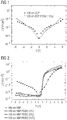
- FIG. 1 shows the result, whereby a 4 mm 2 large component was measured which gave the characteristic curve marked by squares ( FIG. 1 Squares).
- PDW-2 is doped into the BCP layer by co-evaporation.
- the circles in FIG. 1 The marked characteristic differs only insignificantly from the characteristic curve of the pure BCP.
- PDW-2 is generally not usable as an n-dopant, in particular not in an OLED and the typical electronic conductors used therein with a typical HOMO in the range 5.8 - 6.2 eV or a typical LUMO in the range of 3.0 - 2.4 eV.
- NPB bis-N, N, N ', N' - (naphthyl-phenyl) benzidine.
- Luminescence (cd / m 2 ), efficiency (cd / A) and lifetime (h) of organic light-emitting diodes are highly dependent on the exciton density in the light-emitting layer and the quality of the charge carrier injection and are limited among other things by this.
- Doped transport layers have the advantage that only a fraction of the voltage required for operation drops in them relative to the overall structure ( ⁇ 30%). Particularly preferably, the falling voltage is even smaller by a power of ten or more, so that no voltage drop is observed at the transport layers.
- FIG. 3 shows the structure of an OLED with individual functional layers.
- layer 1 represents the substrate, for example of quartz, glass or a metal or polymer film.
- transparent electrode 2 for example an electrode made of a transparent conductive oxide.
- Transparent conductive oxides are transparent, conductive materials, usually metal oxides, such as zinc oxide, tin oxide, cadmium oxide, titanium oxide, indium oxide or indium tin oxide (ITO).
- the electrode (2) may be a (non-transparent) layer of metals.
- the substrate may then be, for example, a non-transparent metal foil.
- ITO anode is shown.
- the hole conductor layer 3 which according to the invention is formed of an organic matrix material which is doped with a metal complex which represents a Lewis acid.
- the emitting layer 4 may be, for example, an organic functional layer, eg based on polymers such as poly (p-phenylene-vinylene) (PPV) or based on so-called low-molecular-weight small molecules (US Pat. "small molecules”) such as tris (8-hydroxyquinolato) aluminum (Alq).
- PPV poly(p-phenylene-vinylene)
- US Pat. "small molecules" such as tris (8-hydroxyquinolato) aluminum (Alq).
- the emitter layer can also consist of many individual emitter layers, for example red, green In addition to the layers 1 to 6 shown, the protection of the OLED by means of an encapsulation is also expedient.
- the electrodes are connected to the voltage source.
- the homogeneity of the charge injection plays an important role. Particles, crystallites or tips cause field elevations and thus potential starting points for "dark spots" which can lead to failure of the luminous element.
- a hole injection layer in which, for example, dinuclear rhodium acetate-based paddle-wheel complexes are embedded, a layer can be produced which exhibits an unexpectedly high current carrying capacity in conjunction with an inherent current limitation.
- Rhodium complexes are preferably used, such as metal complex compounds having a Rh 2 4+ core and a metal-metal bond, which act as p-dopant and electron acceptor due to their high Lewis acid character.
- FIG. 4 shows the structure of Rh 2 (CF 3 COO) 4 , to which the aromatic system hexamethylbenzene is coordinated.
- Rh 2 4+ complexes to this structure in particular those that show similar sizes such as an analog with Ru 2 2+ ions as central atoms are also suitable as p-dopants.
- Particularly suitable are the central atoms or metal complexes suitable as p-dopants, which can coordinate directly to aromatic systems, such as, for example, uncharged aromatic systems.
- aromatic systems such as, for example, uncharged aromatic systems.
- central atoms therefore, especially the metals of the 6th to 9th subgroup are considered
- a paddle-wheel complex at least two, mostly exactly two, metal central atoms, in particular transition metal atoms, are bridged by 1, 2, 3, 4 or more multidentate (in particular bidentate) ligands which each bind a ligand atom to the at least two metal central atoms.
- the metal atoms are here, depending on the radius, usually 4-fold coordinated with the mentioned ligands.
- the Lewis acid character of the paddle-wheel complexes is given in particular by the presence of a loose or empty coordination site on at least one metal atom, at which, for example, the attachment of an aromatic ring, as in US Pat FIG. 4 shown, can take place.
- the coordination environment of the metal atom is preferably such that there is a metal-metal bond and 4 equatorial bonds to ligands. As a rule, therefore, the axial position has the loose or empty coordination site, whereby the complex is Lewis acid depending on the ligand and central atom.
- Suitable ligands are, in particular, all two- or multidentate ligands, preferably electron-withdrawing ligands.
- anions of electron-withdrawing carboxylic acids such as, for example, CH x H 3-x COOH, in particular CF x H 3-x COOH and CCl x H 3 -x COOH (where x is an integer between 0 and 3 and Hal is a halogen atom represents), (CR 1 , R 2 , R 3 ) COOH, where R 1 , R 2 and R 3 independently of one another alkyl, particularly preferably H, methyl, ethyl, propyl, isopropyl, n-butyl, sec-butyl, tert Butyl and benzoic acid and their substituted analogues (o, p, m-fluorobenzoic acid, o, p, m-cyanobenzoic acid, nitrobenzoic, alkylbenzoic with
- the metal complexes used in accordance with the invention are preferably molecules which can be vaporized independently of one another. It is understood that individual metal complexes may each be bonded to each other or to other components such as the matrix material.
- individual metal complexes may each be bonded to each other or to other components such as the matrix material.
- the bond formation of the donor-acceptor interaction and the molecular size fix the dopants in the matrix.
- Suitable organic matrix materials are all common hole conductor matrices, such as NPB; NaphDATA; N, N'-bis, N'-bis -benzidine (naphthalen-1-yl) -N (phenyl); N, N'-bis, N'-bis -benzidine (naphthalen-2-yl) -N (phenyl); N, N'-bis, N'-bis -benzidine (3-methylphenyl) -N (phenyl); N, N'-bis (3-methylphenyl) -N, N'-bis (phenyl) -9,9-spirobifluorenes; N, N'-bis (naphthalen-1-yl) -N, N'-bis (phenyl) -9,9-spirobifluorenes; N, N'-bis (3-methylphenyl) -N, N'-bis (phenyl) -9,9-spirobifluorenes; N, N'-bis (3-methyl
- NPB bis-N, N, N ', N' - (naphthyl-phenyl) benzidine.
- An additional band in the UV spectrum in the range between 550-600 nm shows the dopability of NPB by PDW-2.
- FIG. 6 shows the photoluminescence spectrum of the example described above FIG. 5 illustrated layers.
- the fluorescence of the NPB layer decreases steadily.
- PDW-2 Completely im In line with other dopants, PDW-2 also quenches the fluorescence.
- the voltage in the IV characteristic is reduced from 5.77 V to 5.03 V in order to achieve a current density of 10 mA / cm 2 .
- the efficiency of this diode is thereby significantly improved, as is the case FIG. 7 is apparent.
- the luminance of 1000 cd / m 2 is already reached at 6.18 V with the doped hole injection layer and only at 7.10 V with the undoped hole injection layer ( FIG. 8 ).
- PDW-2 is similar in construction to the example FIG. 5 as efficient as other literature known dopants eg MoO 3 or F 4 TCNQ as the comparison shown here proves.
- the charge carrier density can also be increased in other hole conductors such as naphdata by the PDW-2 dopant.
- the voltage in the IV characteristic is reduced from 11.6 V to 8.0 V in order to achieve a current density of 10 mA / cm 2 .
- the efficiency of this diode is thereby significantly improved (FIG. 11).
- the luminance of 1000 cd / m 2 is already reached at 10.6 V with the doped hole injection layer and only at 13.9 V with the undoped hole injection layer ( FIG. 12 ).
- the invention is characterized in particular by the fact that the materials used are OLED compatible and that, for example, in the preferred binuclear metal complexes with the metal-metal bond formally the charge during current transport in the molecule is distributed to two metal atoms, which contributes to the stability of the overall layer.
- the invention relates to the use of a metal complex as p-dopant for an organic semiconductive matrix material, an organic semiconductor material and an organic light-emitting diode.
- the invention discloses the use of metal complexes which act as Lewis acids as p-dopants in organic matrix materials.
Landscapes
- Chemical & Material Sciences (AREA)
- Engineering & Computer Science (AREA)
- Materials Engineering (AREA)
- Inorganic Chemistry (AREA)
- Manufacturing & Machinery (AREA)
- Physics & Mathematics (AREA)
- Optics & Photonics (AREA)
- Crystallography & Structural Chemistry (AREA)
- Electroluminescent Light Sources (AREA)
- Organic Chemistry (AREA)
Abstract
Description
- Die Erfindung betrifft die Verwendung eines Metallkomplexes als p-Dotand für ein organisches halbleitendes Matrixmaterial, ein organisches Halbleitermaterial und organische Leuchtdiode.
- Die Dotierung organischer halbleitender Materialien mit Elektronenakzeptoren zur Erhöhung der Leitfähigkeit in organischen Matrixmaterialien ist beispielsweise aus der
WO 2005/086251 bekannt. Dort werden Metallkomplexe, insbesondere mehrkernige Metallkomplexe wie die so genannten Schaufelradkomplexe (paddle-wheel) wegen ihrer starken Donoreigenschaften als n-Dotanden für die Elektroneninjektion beschrieben. - Es besteht jedoch ein Bedarf, p-Dotanden zur Dotierung der Lochinjektionsschicht zur Verfügung zu stellen.
- Aufgabe der vorliegenden Erfindung ist es daher, p-Dotanden für eine lochleitende Matrix anzugeben und die Verwendungen derart dotierter lochleitender Matrixmaterialien in einer strahlungsemittierenden Vorrichtung, insbesondere einer organischen Leuchtdiode (OLED), zu offenbaren.
- Diese Aufgabe wird durch die Merkmale der unabhängigen Ansprüche, insbesondere durch die Verwendung von neutralen Metallkomplexen mit Lewis-Säure Charakter als p-Dotanden in lochleitenden organischen Matrixmaterialien gelöst. Ferner wird die Aufgabe durch die Bereitstellung eines organischen halbleitenden Materials mit einer Verbindung eines solchen Metallkomplexes mit Lewis-Säure Charakter als p-Dotand gelöst. Schließlich wird die Aufgabe noch durch die Angabe von OLEDs mit zumindest einer Schicht eines erfindungsgemäßen organischen Matrixmaterials gelöst.
- Gegenstand der Erfindung ist die Verwendung eines neutralen Metallkomplexes mit Lewis-Säure Eigenschaften als p-Dotand eines organischen halbleitenden Matrixmaterials. Weiterhin ist Gegenstand der Erfindung eine Lochleiterschicht, bestehend aus einem lochleitenden organischen Matrixmaterial mit einem Anteil von 0,1 bis 50 (Schichtdicken%) an Metallkomplex als p-Dotanden. Schließlich ist Gegenstand der Erfindung eine OLED, zumindest eine Schicht eines dotierten Lochleitermaterials umfassend, das einen Metallkomplex als p-Dotanden enthält.
- Lewis-Säuren sind Verbindungen, die als Elektronenpaarakzeptoren wirken. Eine Lewis-Base ist dementsprechend ein Elektronenpaardonator, der Elektronenpaare abgeben kann. Insbesondere ist die Lewis-Säure-Eigenschaft der Metallkomplexe in Bezug auf das lochleitende organische Matrixmaterial zu setzen, das dann die korrespondierende Lewis-Base darstellt (bzw. enthält).
- Ein Metallkompex ist eine Verbindung, in der ein Metallatom bzw. Metallion von einem oder mehreren Liganden koordiniert ist. Im Regelfall ist der Metallkomplex eine metallorganische Verbindung, d.h. ein Komplex, bei dem zumindest ein Teil der Liganden Kohlenstoff-haltig und häufig auch Kohlenwasserstoff-haltig ist.
- Vorteilhafterweise handelt es sich bei dem Metallkomplex um einen mehrkernigen Komplex, insbesondere um einen Komplex mit zumindest einer Metall-Metallbindung.
- Nach einer vorteilhaften Ausführungsform ist zumindest ein Zentralatom des Metallkomplexes ausgewählt aus der Gruppe der Platinmetalle, folgende Elemente umfassend: Ruthenium, Rhodium, Palladium, Osmium, Iridium und Platin. Insbesondere sind Rhodiumkomplexe bevorzugt.
- Nach einer vorteilhaften Ausführungsform ist das Zentralatom ein neutrales oder geladenes, insbesondere positiv geladenes, Übergangsmetallatom.
- Unter Lochleitern werden die typische Materialien, die in der OLED lochleitend wirken, wie NPB (N,N'-di-1-napthyl-diphenylbenzidin, HOMO = 5,5 eV; LUMO = 2,4 eV) oder Naphdata (4,4',4''-Tris(N-(1-naphthyl)-N-phenyl -amino)-triphenylamin; HOMO = 5,1 eV; LUMO = 2,3 eV) verstanden.
- Die Dotierung wird im Folgenden in relativen Schichtdicken angeben d.h. x % bedeutet, dass die Depositionsrate des Dotanden x % im Bezug auf die Depositionsrate der Matrix beträgt.
- Vorteilhafterweise wird als neutraler Metallkomplex ein Komplex mit einer so genannten "paddle-wheel / Schaufelrad" Struktur eingesetzt, wobei besonders bevorzugt zwei- und mehrkernige Metallkomplexe mit zumindest einer Metall-MetallBindung verwendet werden, wie sie beispielsweise aus "Cotton FA, Gruhn NE, Gu J, Huang P, Lichtenberger DL, Murillo Ca, Van Dorn LO und Wilkinson CC: "Closed Shell Molecules That Ionize More Readily Than Cesium" in Science, 2002, 298; 1971-1974 bekannt sind. Ebenfalls beschrieben werden diese Strukturen in der
WO 2005/086251 . Dort wird jedoch davon ausgegangen, dass mehrkernige Metallkomplexe mit Schaufelradstruktur "paddle-wheel" als n-Dotanden wirken. Dies trifft aber nicht auf alle Paddle-Wheel-Komplexe bzw. die dort genannten Strukturen zu, wie vorliegend gezeigt werden konnte. - In der
WO 2005/086251 A2 werden Komplexe mit Schaufelradstruktur als typische n-Dotanden vorgestellt. Um die Verwendbarkeit von Dirhodium-tetra-trifluoroacetat (PDW-2), einem typischen Vertreter der Metallkomplexe mit starkem Lewis-Säure Charakter, wie sie vorliegend als p-Dotanden unter Schutz gestellt werden sollen, als n-Dotand zu überprüfen, wurde folgendes Experiment durchgeführt: - Auf einer ITO (Indium-tin-oxide = indiumdotiertes Zinnoxid) Elektrode wurde durch thermisches Verdampfen eine 150 nm dicke Schicht des Elektronenleiters BCP (= 2,9-Dimethyl-4,7-diphenyl-1,10-phenantholin) abgeschieden. Als Gelegenelektrode diente eine 150 nm dicke Aluminiumschicht.
Figur 1 zeigt das Ergebnis, wobei ein 4 mm2 großes Bauelement gemessen wurden das die durch Quadrate markierte typische Kennlinie ergab (Figur 1 Quadrate). - In einem zweiten Experiment werden in die BCP-Schicht durch Koverdampfung 10% PDW-2 eindotiert. Die durch Kreise in
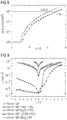
Figur 1 markierte Kennlinie unterscheidet sich nur unwesentlich von der Kennlinie des reinen BCP. Damit ist PDW-2 generell nicht als n-Dotand einsetzbar, insbesondere nicht in einer OLED und den darin verwendeten typischen Elektronenleitern mit einem typischen HOMO im Bereich 5,8 - 6,2 eV bzw. einem typischen LUMO im Bereich von 3,0 - 2,4 eV. - Analog zum oben beschriebenen Experiment wird PDW-2 durch Koverdampfung in den Lochleiter NPB (= Bis-N,N,N',N'-(naphthyl-phenyl)benzidin) eindotiert. Für eine Dotierung von 0% (Kreise voll), 1%( Quadrate), 5%(Dreiecke) und 10% (Kreise leer) ergaben sich die in
Figur 2 dargestellten Kennlinien. - Diese demonstrieren eindeutig die Möglichkeit zur p-Dotierung von lochleitenden Matrixmaterialien durch PDW-2. Erstaunlicherweise können aus Aluminium keine Löcher injiziert werden (negativer Ast der x-Achse), wodurch sich ein Gleichrichtungsfaktor von 3·10-7 ergibt. Für eine effektive Dotierung reichen nur wenige relative Schichtdicken % aus (insbesondere 0 - 50%, besonders bevorzugt 0 - 15 %). Die Kennlinien zwischen 1 - 10% PDW-2 in NPB sind nahezu identisch. Die Kennlinien sind zudem sehr steil. Bei höheren Spannungen sättigt die Kennlinie, wodurch ein strombegrenzendes Verhalten resultiert.
- Die Dotierung organischer Matrixmaterialien mit p-Dotanden ist von entscheidender Relevanz für organische Leuchtdioden. Lumineszenz (cd/m2), Effizienz (cd/A) und Lebensdauer (h) organischer Leuchtdioden hängen stark von der Exzitonendichte in der lichtemittierenden Schicht und der Qualität der Ladungsträgerinjektion ab und werden unter anderem auch durch diese limitiert. Dotierte Transportschichten haben den Vorteil, dass an ihnen relativ zum Gesamtaufbau nur ein Bruchteil der zum Betrieb nötigen Spannung abfällt (<< 30%). Besonders bevorzugt ist die abfallende Spannung sogar um eine Zehnerpotenz oder mehr kleiner, so dass an den Transportschichten kein Spannungsabfall beobachtet wird.
-
Figur 3 zeigt den Aufbau einer OLED mit einzelnen Funktionsschichten. Zu erkennen ist die unterste und gleichzeitig dickste Schicht 1, die das Substrat, beispielsweise aus Quarz, Glas oder einer Metall- oder Polymerfolie, darstellt. Darauf liegt die transparente Elektrode 2, Z.B. eine Elektrode aus einem transparenten leitenden Oxid. Transparente leitende Oxide (transparent conductive oxides, kurz "TCO") sind transparente, leitende Materialien, in der Regel Metalloxide, wie beispielsweise Zinkoxid, Zinnoxid, Cadmiumoxid, Titanoxid, Indiumoxid oder Indiumzinnoxid (ITO). Neben binären Metallsauerstoffverbindungen, wie beispielsweise ZnO, SnO2 oder In2O3 gehören auch ternäre Metallsauerstoffverbindungen, wie beispielsweise 2n2SnO4, CdSnO3, ZnSnO3, MgIn2O4, GaInO3, Zn2In2O5 oder In4Sn3O12 oder Mischungen unterschiedlicher transparenter leitender Oxide zu der Gruppe der TCOs. Weiterhin entsprechen die TCOs nicht zwingend einer stöchiometrischen Zusammensetzung und können auch p- oder n-dotiert sein. Im Fall von Top-emittierenden Dioden kann die Elektrode (2) eine (nicht transparente) Schicht aus Metallen sein. Das Substrat kann dann z.B. eine nicht durchsichtige Metallfolie sein. InFigur 3 ist beispielsweise eine ITO-Anode dargestellt. Auf dieser unteren Elektrode liegt die Lochleiterschicht 3, die gemäß der Erfindung aus einem organischen Matrixmaterial gebildet ist, das mit einem Metallkomplex, der eine Lewissäure darstellt dotiert ist. - Auf der Lochleiterschicht 3 liegt die eigentlich aktive Schicht der OLED, die emittierende Schicht 4. Darauf befindet sich noch die Elektronentransportschicht 5 und die Gegenelektrode 6. Die emittierende Schicht 4 kann z.B. eine organische funktionelle Schicht, z.B. auf der Basis von Polymeren wie Poly(p-phenylen-vinylen) (PPV) oder auf der Basis von so genannten niedermolekularen kleinen Molekülen ("small molecules") wie z.B. Tris(8-hydroxyquinolato)-aluminium (Alq) sein. Weiterhin kann es sich z.B. um phophoreszente Triplettemitter wie Tri(phenylpyridino)Iridium(III), eindotiert in ein Matrixmaterial Bis-N,N'-(carbazoylbiphenyl (CPB), handeln. Die Emitterschicht kann auch aus vielen Einzelemitterschichten bestehen wobei z.B. rotes, grünes oder blaues Licht emittiert wird. Zusätzlich zu den gezeigten Schichten 1 bis 6 ist noch der Schutz der OLED mittels einer Verkapselung zweckmäßig.
- Über die elektrische Leitung 7 werden die Elektroden mit der Spannungsquelle verbunden.
- Bei großflächigen Leuchtelementen spielt die Homogenität der Ladungsinjektion eine wichtige Rolle. Partikel, Kristallite oder Spitzen verursachen Feldüberhöhungen und damit potentielle Ausgangspunkte für "dark spots" die zum Ausfall des Leuchtelements führen können. Durch eine Lochinjektionsschicht, in die beispielsweise zweikernige Rhodiumacetatbasierte "paddle-wheel"-Komplexe eingebettet sind, kann eine Schicht erzeugt werden, die eine unerwartet hohe Stromtragfähigkeit in Verbindung mit einer inhärenten Strombegrenzung zeigt.
- Bevorzugt werden Rhodiumkomplexe eingesetzt, wie Metallkomplex-Verbindungen mit einem Rh2 4+ Kern und einer Metall-Metallbindung, die aufgrund ihres hohen Lewis-Säure-Charakters als p-Dotand und Elektronenakzeptor wirken.
- Besonders bevorzugt ist das Dirhodiumtetratrifluoracetat (
Fig. 4 ), das sich aufgrund seiner günstigen Sublimationseigenschaften sehr gut eignet. In der chemischen Literatur [F. A. Cotton, C. A. Murillo, R. A. Walton "Multiple Bonds between Metal Atoms" 3. Auflage, Springer Science and Business Media, Inc. 2005. 465-611.] konnte unerwarteter Weise auch kristallografisch gezeigt werden, dass sogar unsubstituierte Aromaten als Donor für den Rh2 4+-Kern in axialer Position dienen können. Experimentell konnte durch die Dotierung von NPB oder Naphdata (Naphdata =4,4',4"-Tris((N-naphthyl)-N-phenyl-amino)-triphenylamin)mit PDW-2 in oben beschriebenen Experimenten gezeigt werden, dass dieser Vorgang eine p-Dotierung bewirkt. -
Figur 4 zeigt die Struktur von Rh2(CF3COO)4, an die das aromatische System Hexamethylbenzol koordiniert ist. - Auch die zu Rh2 4+-Komplexen isoelektronischen Metallkomplexe zu dieser Struktur, insbesondere solche, die noch ähnliche Größen zeigen wie beispielsweise ein Analogon mit Ru2 2+-Ionen als Zentralatome sind ebenfalls geeignet als p-Dotanden. Diese bewirken zum einen die Schaufelradstruktur und zum anderen die sehr hohe Lewis-Säure Azidität dieser Komplexe. Insbesondere geeignet sind die als p-Dotanden geeigneten Zentralatome bzw. Metallkomplexe, die direkt an aromatische Systeme, wie z.B. ungeladene aromatische Systeme koordinieren können. Als Zentralatome kommen daher insbesondere die Metalle der 6. bis 9. Nebengruppe in Betracht
- Bei einem paddle-wheel-Komplex sind mindestens zwei, zumeist genau zwei Metallzentralatome insbesondere Übergangsmetallatome, durch 1, 2 ,3 ,4 oder mehr mehrzähnige (insbesondere zweizähnige) Liganden, die an die mindestens zwei Metallzentralatome jeweils ein Ligandenatom binden, überbrückt. Die Metallatome sind hierbei, je nach Radius, zumeist 4-fach mit den genannten Liganden koordiniert.
- Der Lewissäurecharakter der paddle-wheel-Komplexe ist insbesondere dadurch gegeben, dass zumindest an einem Metallatom eine lockere oder leere Koordinationsstelle vorhanden ist, an der beispielsweise die Anlagerung eines aromatischen Ringes, wie in
Figur 4 gezeigt, stattfinden kann. Die Koordinationsumgebung des Metallatoms ist bevorzugt so, dass eine Metall-Metall-Bindung besteht sowie 4 äquatoriale Bindungen zu Liganden. Im Regelfall weist daher die axiale Position die lockere oder leere Koordinationsstelle auf, wodurch der Komplex je nach Ligand und Zentralatom Lewis-azid ist. - Als Liganden eignen sich insbesondere alle zwei -oder mehrzähnigen Liganden, bevorzugt elektronenziehende Liganden. Beispielsweise genannt seien die Anionen von elektronenziehenden Carbonsäuren, wie beispielsweise CHalxH3-xCOOH, insbesondere CFxH3-xCOOH und CClxH3-xCOOH (wobei x eine ganze Zahl zwischen 0 und 3 ist und Hal ein Halogenatom darstellt), (CR1, R2, R3) COOH, wobei R1, R2 und R3 unabhängig voneinander Alkyl, wie besonders bevorzugt H, methyl, ethyl, propyl, isopropyl, n- Butyl, sec- Butyl, tert-Butyl, sowie Benzoesäure und deren substituierte Analoga (o, p, m-Fluorbenzoesäure, o,p,m- Cyanobenzoesäure, Nitrobenzoesäure, Alkylbenzoesäuren mit fluorierten oder teilweise fluorierten Alkylgruppen, ggf. auch ein oder mehrfach substituiert, Pyridincarbonsäuren etc.) sein kann.
- Die erfindungsgemäß verwendeten Metallkomplexe stellen vorzugsweise Moleküle dar, die unabhängig voneinander verdampfbar sind. Dabei versteht sich, dass einzelne Metallkomplexe jeweils untereinander oder mit anderen Komponenten wie dem Matrixmaterial gebunden sein können.
- Rein formal könnten die Valenzelektronen des PDW-2 wie folgt berechnet werden:
- In der Gruppe IX mit 4 einfach negativ geladenen zweizähnigen Liganden ergibt sich folgendes Bild für Metall-Metall:
- 4 x 4e = 16 Elektronen von den Liganden
- 1 x 2e = 2 von der Einfachfachbindung zwischen Rh-Rh
- 2 x 9e = 18 vom Rhodium
- Summe 36, damit hat jedes Rh Edelgaskonfiguration d.h. stabil Alternativ ergibt sich die Summe 36 für andere Metalle bei gleichen Liganden:
- Metalle der Gruppe 6: Metall - Metall-Vierfachbindung d.h. σ, 2 x π, 1 x δ-Bindung besetzt
- Metalle der Gruppe 7: Metall - Metall-Dreifachbindung d.h. σ, 2 x π, 1 x δ-Bindung, 1 x δ* besetzt
- Metalle der Gruppe 8: Metall - Metall-Zweifachbindung d.h. σ, 2 x π, 1 x δ-Bindung, 1 x δ*, 1 x π* besetzt
- Metalle der Gruppe 9: Metall - Metall-Einfachbindung d.h. σ, 2 x π, 1 x δ-Bindung, 1 x δ*, 2 x π* besetzt
- Dabei versteht sich, dass einzelne Metallkomplexe jeweils untereinander oder mit anderen Komponenten wie dem Matrixmaterial gebunden sein können. Durch die Bindungsbildung der Donator-Akzeptorwechselwirkung und die Molekülgröße werden die Dopanten in der Matrix fixiert.
- Als organische Matrixmaterialien eignen sich alle gängigen Lochleitermatrizen, wie beispielsweise NPB; Naphdata; N,N'-Bis(naphthalen-1-yl)-N,N'-bis(phenyl)-benzidine; N,N'-Bis(naphthalen-2-yl)-N,N'-bis(phenyl)-benzidine; N,N'-Bis(3-methylphenyl)-N,N'-bis(phenyl)-benzidine; N,N'-Bis(3-methylphenyl)-N,N'-bis(phenyl)-9,9-spirobifluorene; N,N'-Bis(naphthalen-1-yl)-N,N'-bis(phenyl)-9,9-spirobifluorene; N,N'-Bis(3-methylphenyl)-N,N'-bis(phenyl)-9,9-dimethyl-fluorene; N,N'-Bis(3-naphthalen-1-yl)-N,N'-bis(phenyl)-9,9-dimethyl-fluorene; N,N'-Bis(3-methylphenyl)-N,N'-bis(phenyl)-9,9-diphenyl-fluorene; N,N'-Bis(3-naphthalen-1-yl)-N,N'-bis(phenyl)-9,9-diphenyl-fluorene; 2,2',7,7'-Tetrakis(N,N-diphenylamino)-9,9'-spirobifluorene; 9,9-Bis[4-(N,N-bis-biphenyl-4-yl-amino)phenyl]-9H-fluorene; 9,9-Bis[4-(N,N-bis-naphthalen-2-yl-amino)phenyl]-9H-fluorene; 9,9-Bis[4-(N,N'-bis-naphthalen-2-yl-N,N'-bis-phenyl-amino)-phenyl]-9H-fluorene; 2,2',7,7'-Tetrakis[(N-naphthalenyl(phenyl)-amino]-9,9-spirobifluorene; N,N'-bis(phenanthren-9-yl)-N,N'-bis(phenyl)-benzidine; 2,7-Bis[N,N-bis(9,9-spiro-bifluorene-2-yl)-amino]-9,9-spirobifluorene; 2,2'-Bis[N,N-bis(biphenyl-4-yl)amino]-9,9-spirobifluorene; 2,2'-Bis(N,N-di-phenyl-amino)-9,9-spirobifluorene; Phthalocyanine-Coppercomplex; 4,4',4"-Tris(N-3-methylphenyl-N-phenyl-amino)triphenylamine; 4,4',4"-Tris(N-(2-naphthyl)-N-phenyl-amino)triphenylamine; 4,4',4"-Tris(N-(1-naphthyl)-N-phenyl-amino)triphenylamine; 4,4',4"-Tris(N,N-diphenyl-amino)triphenylamine; Titanium oxide phthalocyanine; 2,3,5,6-Tetrafluoro-7,7,8,8,-tetracyano-quinodimethane; Pyrazino[2,3-f][1,10]phenanthrolone-2,3-dicarbonitrile; N,N,N',N'-Tetrakis(4-methoxyphenyl)benzidine; 2,7-Bis[N,N-bis(4-methoxy-phenyl)amino]-9,9-spirobifluorene; 2,2'-Bis[N,N-bis(4-methoxy-phenyl)amino]-9,9-spirobifluorene; 1,3-Bis(carbazol-9-yl)benzene; 1,3,5-Tris(carbazol-9-yl)benzene; 4,4',4"-Tris(carbazol-9-yl)triphenylamine; 4,4'-Bis(carbazol-9-yl)biphenyl; 4,4'-Bis(9- carbazolyl)-2,2'-dimethyl-biphenyl; 2,7-Bis(carbazol-9-yl)-9,9-dimentylfluorene und 2,2',7,7'-Tetrakis(carbazol-9-yl)-9,9'-spirobifluorene.
- Die experimentell gefundene Strombegrenzung wurde bisher bei keiner der publizierten für die Dotierung geeigneten Materialsysteme beobachtet. Dieser Aspekt ist für großflächige organische Leuchtdioden besonders wichtig, da er eine Homogenisierung der Leuchtdichte bewirkt. Feldüberhöhungen an Partikeln oder Spitzen im Substratmaterial werden durch Schichten mit Strombegrenzung ausgeglichen, da der maximale Stromfluss nicht mehr vom angelegten Feld abhängt.
- Im Folgenden wird die Erfindung noch anhand einiger experimenteller Ergebnisse verdeutlicht:
- Analog zum oben beschriebenen Experiment wird PDW-2 durch Koverdampfung in den Lochleiter NPB (= Bis-N,N,N',N'-(naphthyl-phenyl)benzidin) eindotiert. Für eine Dotierung von 0%, 1%, 5% und 10% und 100% PDW2 ergeben sich die in
Figur 5 dargestellten Kennlinien. - Eine zusätzliche Bande im UV-Spektrum im Bereich zwischen 550-600 nm zeigt die Dotierfähigkeit von NPB durch PDW-2.
- Die Grafik von
Figur 6 zeigt das Photolumineszenzspektrum der im oben beschriebenen Beispiel zuFigur 5 dargestellten Schichten. Bei Anregung der Schicht mit UV-Licht von 342 nm nimmt die Fluoreszenz der NPB Schicht stetig ab. Ganz im Einklang zu anderen Dotanten löscht auch PDW-2 die Fluoreszenz. - Auf einer ITO (Indium-tin-oxide = indiumdotiertes Zinnoxid) Elektrode werden nacheinander durch thermisches Verdampfen folgende Schichten abgeschieden, um eine organische Leuchtdiode auf zu bauen (Alq = Aluminiumtrishydroxychinolinat, LiF = Lithiumfluorid).
- a. 50 nm NPB; 40 nm NPB; 40 nm Alq; 0.7 nm LiF; 200 nm Al (Kreise voll)
- b. 50 nm NPB:PDW-2 [10%]; 40 nm NPB; 40 nm Alq; 0.7 nm LiF; 200 nm Al (Kreise leer)
- Durch den Einsatz der dotierten Lochinjektionsschicht wird in der I-V-Kennlinie die Spannung von 5.77 V auf 5.03 V reduziert, um eine Stromdichte von 10 mA/cm2 zu erreichen. Die Effizienz dieser Diode wird dadurch deutlich verbessert, wie aus
Figur 7 ersichtlich ist. - Durch die Reduzierung der Versorgungsspannung wird die Leuchtdichte von 1000 cd/m2 schon bei 6.18 V mit der dotierten Lochinjektionsschicht und erst bei 7.10V mit der undotierten Lochinjektionsschicht erreicht (
Figur 8 ). - PDW-2 ist in Aufbauten analog dem Beispiel zu
Figur 5 ähnlich effizient, wie andere literaturbekannte Dopanden z.B. MoO3 oder F4TCNQ wie der hier gezeigte Vergleich beweist. - Die Ladungsträgerdichte kann in anderen Lochleitern wie Naphdata durch den Dopanden PDW-2 ebenfalls erhöht werden.
- Transiente Dunkelstrommessungen zeigen, dass bei einer Dotierung von 10% PDW-2 in Naphdata die Mobilität nahezu konstant bleibt. Wie das Beispiel zu
Fig. 10 demonstriert, steigt die für die organische Leuchtdiode zur Verfügung stehende Ladungsträgerdichte stark an, was sich sehr positiv auf die Kennlinien von organischen Leuchtdioden auswirkt. - (σ = Leitfähigkeit, µ = Mobilität, n = Zahl der Ladungsträger, e = Elementarladung)
- Eine analog Beispiel zu
Figur 7 aufgebaute Leuchtdiode mit Naphdata statt NPB in der Lochinjektionsschicht. - a. 50 nm Naphdata; 40 nm NPB; 40 nm Alq; 0.7 nm LiF; 200 nm Al (Kreise voll)
- b. 50 nm Naphdata:PDW-2 [10%]; 40 nm NPB; 40 nm Alq; 0.7 nm LiF; 200 nm Al (Kreise leer)
- Durch den Einsatz der dotierten Lochinjektionsschicht wird in der I-V-Kennlinie die Spannung von 11.6 V auf 8.0 V reduziert, um eine Stromdichte von 10 mA/cm2 zu erreichen. Die Effizienz dieser Diode wird dadurch deutlich verbessert (Figur 11)
- Durch die Reduzierung der Versorgungsspannung wird die Leuchtdichte von 1000 cd/m2 schon bei 10.6 V mit der dotierten Lochinjektionsschicht und erst bei 13.9 V mit der undotierten Lochinjektionsschicht erreicht (
Figur 12 ). - Die experimentell gefundene Strombegrenzung wurde bisher bei keiner der publizierten für die Dotierung geeigneten Materialsysteme beobachtet. Dieser Aspekt ist für großflächige organische Leuchtdioden besonders wichtig, da er eine Homogenisierung der Leuchtdichte bewirkt. Feldüberhöhungen an Partikeln oder Spitzen im Substratmaterial werden durch Schichten mit Strombegrenzung ausgeglichen, da der maximale Stromfluss nicht mehr vom angelegten Feld abhängt.
- Die Erfindung zeichnet sich insbesondere dadurch aus, dass die verwendeten Materialien OLED kompatibel sind und dass beispielsweise in den bevorzugten zweikernigen Metallkomplexen mit der Metall-Metallbindung formal die Ladung beim Stromtransport im Molekül auf zwei Metallatome verteilt wird, was zur Stabilität der Gesamtschicht beiträgt.
- Die Erfindung betrifft die Verwendung eines Metallkomplexes als p-Dotand für ein organisches halbleitendes Matrixmaterial, ein organisches Halbleitermaterial und eine organische Leuchtdiode. Die Erfindung offenbart dabei die Verwendung von Metallkomplexen, die als Lewis-Säuren fungieren als p-Dotanden in organischen Matrixmaterialien.
- Bevorzugte Ausführungsformen:
- 1. Verwendung eines Metallkomplexes als p-Dotand zur Dotierung eines lochleitenden organischen Matrixmaterials, wobei der Metallkomplex ein Metallkomplex mit Lewissäureeigenschaft ist und als Elektronenpaarakzeptor wirkt.
- 2. Verwendung nach Ausführungsform 1, wobei der Metallkomplex ein mehrkerniger Metallkomplex ist.
- 3. Verwendung nach einer der vorstehenden Ausführungsformen 1 oder 2, wobei das Zentralatom des Metallkomplexes ein neutrales oder geladenes Übergangsmetallatom ist.
- 4. Verwendung nach einer der vorstehenden Ausführungsformen, wobei zumindest ein Zentralatom aus der 6. bis 9. Nebengruppe ausgewählt ist.
- 5. Verwendung nach der vorhergehenden Ausführungsform, wobei zumindest ein Zentralatom Rhodium ist.
- 6. Verwendung nach einer der vorstehenden Ausführungsformen, wobei der Metallkomplex ein mehrkerniger Metallkomplex ist, bei dem zumindest ein Ligand zwei Zentralatome koordinativ verbindet.
- 7. Verwendung nach einer der vorstehenden Ausführungsformen, wobei zumindest ein Zentralatom quadratisch planar von Liganden umgeben ist.
- 8. Verwendung nach einer der vorstehenden Ausführungsformen, wobei der Metallkomplex mehrkernig und symmetrisch aufgebaut ist.
- 9. Verwendung nach einer der vorstehenden Ausführungsformen, wobei die Liganden Carbonsäuren oder Carbonsäureanionen mit elektronenziehenden Substituenten sind.
- 10. Verwendung nach einer der vorstehenden Ausführungsformen, wobei zumindest ein Metallkomplex eine Schaufelradstruktur hat.
- 11. Halbleitendes Material, insbesondere organisches halbleitendes Material enthaltend zumindest ein organisches Matrixmaterial und einen p-Dotanden nach einem der Ausführungsformen 1 bis 10.
- 12. Organisches halbleitendes Material nach Ausführungsform 11, wobei das molare Dotierungsverhältnis von p-Dotand zu monomeren Einheiten eines polymeren Matrixmoleküls zwischen 1:1 und 1:100.000 beträgt.
- 13. Verfahren zur Herstellung eines organischen halbleitenden Materials enthaltend ein organisches Matrixmaterial und einen p-Dotanden, wobei als p-Dotand zumindest ein oder mehrere Metallkomplexe nach einem der Ausführungsformen 1 bis 10 verwendet werden.
- 14. Strahlungsemittierende Vorrichtung enthaltend ein organisches halbleitendes Material nach Ausführungsform 11 oder 12.
- 15. Strahlungsemittierende Vorrichtung nach der vorhergehenden Ausführungsform, wobei die strahlungsemittiernde Vorrichtung eine organische Leuchtdiode ist, die zwei Elektroden eine Lochleitschicht und eine emittierende Schicht umfasst, wobei die Lochleitschicht einen oder mehrere Metallkomplexe nach einem der Ausführungsformen 1 bis 10 enthält.
- Die Erfindung ist nicht durch die Beschreibung anhand der Ausführungsbeispiele beschränkt. Vielmehr umfasst die Erfindung jedes neue Merkmal sowie jede Kombination von Merkmalen, was insbesondere jede Kombination von Merkmalen in den Patentansprüchen beinhaltet, auch wenn dieses Merkmal oder diese Kombination selbst nicht explizit in den Patentansprüchen oder Ausführungsbeispielen angegeben ist.
Claims (17)
- Verwendung eines Metallkomplexes als p-Dotand zur Dotierung eines lochleitenden organischen Matrixmaterials, wobei der Metallkomplex ein Metallkomplex mit Lewissäureeigenschaft ist und als Elektronenpaarakzeptor wirkt und die Liganden Carbonsäuren oder Carbonsäureanionen mit elektronenziehenden Substituenten sind.
- Verwendung nach Anspruch 1, wobei der Metallkomplex ein mehrkerniger Metallkomplex ist.
- Verwendung nach einem der vorstehenden Ansprüche 1 oder 2, wobei das Zentralatom des Metallkomplexes ein neutrales oder geladenes Übergangsmetallatom ist.
- Verwendung nach einem der vorstehenden Ansprüche, wobei zumindest ein Zentralatom aus der 6. bis 9. Nebengruppe ausgewählt ist.
- Verwendung nach dem vorhergehenden Anspruch, wobei zumindest ein Zentralatom Rhodium ist.
- Verwendung nach einem der vorstehenden Ansprüche, wobei der Metallkomplex ein mehrkerniger Metallkomplex ist, bei dem zumindest ein Ligand zwei Zentralatome koordinativ verbindet.
- Verwendung nach einem der vorstehenden Ansprüche, wobei zumindest ein Zentralatom quadratisch planar von Liganden umgeben ist.
- Verwendung nach einem der vorstehenden Ansprüche, wobei der Metallkomplex mehrkernig und symmetrisch aufgebaut ist.
- Verwendung nach einem der vorstehenden Ansprüche, wobei die Liganden Anionen von elektronenziehenden Carbonsäuren sind und die Carbonsäuren Benzoesäuren oder substituierte Benzoesäuren sind.
- Verwendung nach einem der vorstehenden Ansprüche, wobei die Liganden Anionen von elektronenziehenden Carbonsäuren sind und die Carbonsäuren Alkylbenzoesäuren mit fluorierten oder teilweise fluorierten Alkylgruppen sind.
- Verwendung nach einem der vorstehenden Ansprüche 1 bis 9, wobei die Liganden Anionen von elektronenziehenden Carbonsäuren sind und die Carbonsäuren o, p, m-Fluorbenzoesäuren, o,p,m- Cyanobenzoesäuren oder Nitrobenzoesäuren sind.
- Verwendung nach einem der vorstehenden Ansprüche, wobei der Metallkomplex eine Schaufelradstruktur hat.
- Halbleitendes Material, insbesondere organisches halbleitendes Material enthaltend zumindest ein organisches Matrixmaterial und einen p-Dotanden, wobei der p-Dotand ein Metallkomplex mit Lewissäureeigenschaft ist, der als Elektronenpaarakzeptor wirkt und die Liganden des Metallkomplexes Carbonsäuren oder Carbonsäureanionen mit elektronenziehenden Substituenten sind.
- Halbleitendes Material nach Anspruch 13, wobei das molare Dotierungsverhältnis von p-Dotand zu monomeren Einheiten eines polymeren Matrixmoleküls zwischen 1:1 und 1:100.000 beträgt.
- Verfahren zur Herstellung eines halbleitenden Materials nach einem der Ansprüche 13 bis 14.
- Strahlungsemittierende Vorrichtung enthaltend ein halbleitendes Material nach einem der Ansprüche 13 bis 14.
- Strahlungsemittierende Vorrichtung nach dem vorhergehenden Anspruch, wobei die strahlungsemittiernde Vorrichtung eine organische Leuchtdiode ist, die zwei Elektroden, eine Lochleitschicht und eine emittierende Schicht umfasst, wobei die Lochleitschicht das halbleitende Material enthält.
Applications Claiming Priority (3)
| Application Number | Priority Date | Filing Date | Title |
|---|---|---|---|
| DE102007028238A DE102007028238A1 (de) | 2007-06-20 | 2007-06-20 | Verwendung eines Metallkomplexes als p-Dotand für ein organisches halbleitendes Matrixmaterial, organisches Halbleitermaterial und organische Leuchtdiode |
| EP08773272.3A EP2158625B1 (de) | 2007-06-20 | 2008-06-18 | Verwendung eines metallkomplexes als p-dotand für ein organisches halbleitendes matrixmaterial, organisches halbleitermaterial und organische leuchtdioden |
| PCT/DE2008/001033 WO2008154914A1 (de) | 2007-06-20 | 2008-06-18 | Verwendung eines metallkomplexes als p-dotand für ein organisches halbleitendes matrixmaterial, organisches halbleitermaterial und organische leuchtdioden |
Related Parent Applications (2)
| Application Number | Title | Priority Date | Filing Date |
|---|---|---|---|
| EP08773272.3A Division-Into EP2158625B1 (de) | 2007-06-20 | 2008-06-18 | Verwendung eines metallkomplexes als p-dotand für ein organisches halbleitendes matrixmaterial, organisches halbleitermaterial und organische leuchtdioden |
| EP08773272.3A Division EP2158625B1 (de) | 2007-06-20 | 2008-06-18 | Verwendung eines metallkomplexes als p-dotand für ein organisches halbleitendes matrixmaterial, organisches halbleitermaterial und organische leuchtdioden |
Publications (2)
| Publication Number | Publication Date |
|---|---|
| EP3157072A1 true EP3157072A1 (de) | 2017-04-19 |
| EP3157072B1 EP3157072B1 (de) | 2023-03-22 |
Family
ID=39720107
Family Applications (3)
| Application Number | Title | Priority Date | Filing Date |
|---|---|---|---|
| EP16203230.4A Withdrawn EP3157073A1 (de) | 2007-06-20 | 2008-06-18 | Verwendung eines metallkomplexes als p-dotand für ein or-ganisches halbleitendes matrixmaterial, organisches halb-leitermaterial und organische leuchtdiode |
| EP08773272.3A Active EP2158625B1 (de) | 2007-06-20 | 2008-06-18 | Verwendung eines metallkomplexes als p-dotand für ein organisches halbleitendes matrixmaterial, organisches halbleitermaterial und organische leuchtdioden |
| EP16203223.9A Active EP3157072B1 (de) | 2007-06-20 | 2008-06-18 | Verwendung eines metallkomplexes als p-dotand für ein organisches halbleitendes matrixmaterial, organisches halbleitermaterial und organische leuchtdiode |
Family Applications Before (2)
| Application Number | Title | Priority Date | Filing Date |
|---|---|---|---|
| EP16203230.4A Withdrawn EP3157073A1 (de) | 2007-06-20 | 2008-06-18 | Verwendung eines metallkomplexes als p-dotand für ein or-ganisches halbleitendes matrixmaterial, organisches halb-leitermaterial und organische leuchtdiode |
| EP08773272.3A Active EP2158625B1 (de) | 2007-06-20 | 2008-06-18 | Verwendung eines metallkomplexes als p-dotand für ein organisches halbleitendes matrixmaterial, organisches halbleitermaterial und organische leuchtdioden |
Country Status (8)
| Country | Link |
|---|---|
| US (1) | US8513702B2 (de) |
| EP (3) | EP3157073A1 (de) |
| JP (1) | JP5559044B2 (de) |
| KR (3) | KR101691780B1 (de) |
| CN (1) | CN101785127B (de) |
| DE (1) | DE102007028238A1 (de) |
| TW (1) | TWI374925B (de) |
| WO (1) | WO2008154914A1 (de) |
Families Citing this family (12)
| Publication number | Priority date | Publication date | Assignee | Title |
|---|---|---|---|---|
| US8633475B2 (en) * | 2010-07-16 | 2014-01-21 | Idemitsu Kosan Co., Ltd. | Organic electroluminescence device and a method for producing the device |
| DE102010056519B4 (de) | 2010-12-27 | 2024-11-28 | Heliatek Gmbh | Optoelektronisches Bauelement mit dotierten Schichten |
| DE102011003192B4 (de) | 2011-01-26 | 2015-12-24 | Siemens Aktiengesellschaft | Halbleiterbauelement und Verfahren zu seiner Herstellung |
| DE102012209523A1 (de) | 2012-06-06 | 2013-12-12 | Osram Opto Semiconductors Gmbh | Hauptgruppenmetallkomplexe als p-Dotanden für organische elektronische Matrixmaterialien |
| DE102012209520A1 (de) * | 2012-06-06 | 2013-12-12 | Osram Opto Semiconductors Gmbh | Metallkomplexe als p-Dotanden für organische elektronische Matrixmaterialien |
| GB201309668D0 (en) | 2013-05-30 | 2013-07-17 | Isis Innovation | Organic semiconductor doping process |
| DE102013106949A1 (de) | 2013-07-02 | 2015-01-08 | Osram Opto Semiconductors Gmbh | Optoelektronisches Bauelement, organische funktionelle Schicht und Verfahren zur Herstellung eines optoelektronischen Bauelements |
| KR102442614B1 (ko) | 2015-08-07 | 2022-09-14 | 삼성디스플레이 주식회사 | 디벤조보롤계 화합물 및 이를 포함한 유기 발광 소자 |
| KR102615114B1 (ko) | 2016-08-23 | 2023-12-19 | 삼성디스플레이 주식회사 | 보롤 화합물 및 이를 포함한 유기 발광 소자 |
| KR101836041B1 (ko) | 2016-08-30 | 2018-03-07 | 메르크 파텐트 게엠베하 | 금속 착물 |
| DE102017111425A1 (de) | 2017-05-24 | 2018-11-29 | Osram Oled Gmbh | Organisches elektronisches Bauelement und Verfahren zur Herstellung eines organischen elektronischen Bauelements |
| EP3859808B1 (de) | 2020-01-28 | 2025-12-24 | Novaled GmbH | Organische elektronische vorrichtung mit einer lochinjektionsschicht, die eine lochtransportverbindung umfasst |
Citations (3)
| Publication number | Priority date | Publication date | Assignee | Title |
|---|---|---|---|---|
| JPH03208689A (ja) * | 1990-01-12 | 1991-09-11 | Dainippon Printing Co Ltd | 光情報記録媒体及びその製造方法 |
| EP1289030A1 (de) * | 2001-09-04 | 2003-03-05 | Sony International (Europe) GmbH | Dotierung eines Lochleitermaterials |
| WO2005086251A2 (de) | 2004-03-03 | 2005-09-15 | Novaled Gmbh | Verwendung von metallkomplexen als n-dotanden für organische halbleiter und die darstellung derselbigen inkl. ihrer liganden |
Family Cites Families (24)
| Publication number | Priority date | Publication date | Assignee | Title |
|---|---|---|---|---|
| US3644454A (en) * | 1968-11-01 | 1972-02-22 | Allied Chem | Chromium complexes of fluorocarbon acids |
| DE4411360A1 (de) * | 1994-03-31 | 1995-10-05 | Wacker Chemie Gmbh | Verfahren zur Herstellung von Carboxylgruppen aufweisenden Organosiliciumverbindungen |
| AU2003289001A1 (en) | 2002-12-19 | 2004-07-29 | Semiconductor Energy Laboratory Co., Ltd. | Light-emitting device and method for manufacturing same |
| ATE471950T1 (de) * | 2002-12-20 | 2010-07-15 | Exxonmobil Chem Patents Inc | Polymerisationsverfahren |
| DE10347856B8 (de) * | 2003-10-10 | 2006-10-19 | Colorado State University Research Foundation, Fort Collins | Halbleiterdotierung |
| US20070185343A1 (en) * | 2004-02-26 | 2007-08-09 | Universiteit Gent | Metal complexes for use in olefin metathesis and atom group transfer reactions |
| EP1763532B1 (de) * | 2004-07-05 | 2007-10-10 | Solvias AG | 1,1'diphosphinoferrocene mit 2,2'-gebundenen achiralen oder chiralen resten |
| ATE490986T1 (de) * | 2005-01-21 | 2010-12-15 | Nippon Soda Co | Polymer, vernetztes polymer, zusammensetzung für ein feststoffpolymer-elektrolyt, feststoffpolymer-elektrolyt und klebstoffzusammensetzung |
| GB0517137D0 (en) * | 2005-08-22 | 2005-09-28 | Viacatt N V | Multicoordinated metal complexes for use in metalthesis reactions |
| US8147986B2 (en) * | 2005-09-30 | 2012-04-03 | Fujifilm Corporation | Organic electroluminescent device |
| EP1786050B1 (de) * | 2005-11-10 | 2010-06-23 | Novaled AG | Dotiertes organisches Halbleitermaterial |
| JP2007141736A (ja) * | 2005-11-21 | 2007-06-07 | Fujifilm Corp | 有機電界発光素子 |
| JP2007157629A (ja) * | 2005-12-08 | 2007-06-21 | Fujifilm Corp | 有機電界発光素子 |
| JP2007200938A (ja) * | 2006-01-23 | 2007-08-09 | Fujifilm Corp | 有機電界発光素子 |
| US7968904B2 (en) * | 2006-02-06 | 2011-06-28 | Fujifilm Corporation | Organic electroluminescence device |
| JP4896544B2 (ja) * | 2006-03-06 | 2012-03-14 | 富士フイルム株式会社 | 有機電界発光素子 |
| EP1860709B1 (de) | 2006-05-24 | 2012-08-08 | Novaled AG | Verwendung von quadratisch planaren Übergangsmetallkomplexen als Dotand |
| US7663309B2 (en) * | 2006-09-28 | 2010-02-16 | Fujifilm Corporation | Organic electroluminescent element having plurality of light emitting layers with specific thicknesses |
| DE102006054523B4 (de) | 2006-11-20 | 2009-07-23 | Novaled Ag | Dithiolenübergangsmetallkomplexe und Selen-analoge Verbindungen, deren Verwendung als Dotand, organisches halbleitendes Material enthaltend die Komplexe, sowie elektronische oder optoelektronisches Bauelement enthaltend einen Komplex |
| DE102006054524B4 (de) | 2006-11-20 | 2022-12-22 | Novaled Gmbh | Verwendung von Dithiolenübergangsmetallkomplexen und Selen- analoger Verbindungen als Dotand |
| WO2008073409A2 (en) | 2006-12-12 | 2008-06-19 | E. I. Du Pont De Nemours And Company | Composite organic encapsulants |
| US20080187748A1 (en) * | 2007-02-07 | 2008-08-07 | Masayuki Mishima | Organic electroluminescence device |
| JP5117199B2 (ja) * | 2007-02-13 | 2013-01-09 | 富士フイルム株式会社 | 有機電界発光素子 |
| DE102007028236A1 (de) | 2007-06-20 | 2009-01-02 | Siemens Ag | Halbleitendes Material und organische Gleichrichterdiode |
-
2007
- 2007-06-20 DE DE102007028238A patent/DE102007028238A1/de not_active Ceased
-
2008
- 2008-06-18 US US12/665,934 patent/US8513702B2/en active Active
- 2008-06-18 WO PCT/DE2008/001033 patent/WO2008154914A1/de not_active Ceased
- 2008-06-18 EP EP16203230.4A patent/EP3157073A1/de not_active Withdrawn
- 2008-06-18 JP JP2010512514A patent/JP5559044B2/ja active Active
- 2008-06-18 CN CN200880103120.7A patent/CN101785127B/zh active Active
- 2008-06-18 KR KR1020167018569A patent/KR101691780B1/ko active Active
- 2008-06-18 EP EP08773272.3A patent/EP2158625B1/de active Active
- 2008-06-18 EP EP16203223.9A patent/EP3157072B1/de active Active
- 2008-06-18 KR KR1020157022753A patent/KR101716600B1/ko active Active
- 2008-06-18 KR KR1020107001189A patent/KR101645042B1/ko active Active
- 2008-06-19 TW TW097122794A patent/TWI374925B/zh active
Patent Citations (3)
| Publication number | Priority date | Publication date | Assignee | Title |
|---|---|---|---|---|
| JPH03208689A (ja) * | 1990-01-12 | 1991-09-11 | Dainippon Printing Co Ltd | 光情報記録媒体及びその製造方法 |
| EP1289030A1 (de) * | 2001-09-04 | 2003-03-05 | Sony International (Europe) GmbH | Dotierung eines Lochleitermaterials |
| WO2005086251A2 (de) | 2004-03-03 | 2005-09-15 | Novaled Gmbh | Verwendung von metallkomplexen als n-dotanden für organische halbleiter und die darstellung derselbigen inkl. ihrer liganden |
Non-Patent Citations (3)
| Title |
|---|
| COTTON FA; GRUHN NE; GU J; HUANG P; LICHTENBERGER DL; MURILLO CA; VAN DORN LO; WILKINSON CC: "Closed Shell Molecules That Ionize More Readily Than Cesium", SCIENCE, vol. 298, 2002, pages 1971 - 1974 |
| F.A. COTTON, E.V. CIKAREV, M.A. PETRUKHINA, S.-E. STIRIBA, POLYHEDRON, vol. 19, 2000, pages 1829 - 1835, XP002494592 * |
| KRUEGER J ET AL: "MODIFICATION OF TIO2 HETEROJUNCTIONS WITH BENZOIC ACID DERIVATIVES IN HYBRID MOLECULAR SOLID-STATE DEVICES", ADVANCED MATERIALS, WILEY - V C H VERLAG GMBH & CO. KGAA, DE, vol. 12, no. 6, 16 March 2000 (2000-03-16), pages 447 - 451, XP000923878, ISSN: 0935-9648, DOI: 10.1002/(SICI)1521-4095(200003)12:6<447::AID-ADMA447>3.0.CO;2-8 * |
Also Published As
| Publication number | Publication date |
|---|---|
| EP3157073A1 (de) | 2017-04-19 |
| DE102007028238A1 (de) | 2008-12-24 |
| EP2158625A1 (de) | 2010-03-03 |
| KR101691780B1 (ko) | 2017-01-09 |
| JP2010530618A (ja) | 2010-09-09 |
| TW200909561A (en) | 2009-03-01 |
| CN101785127A (zh) | 2010-07-21 |
| US8513702B2 (en) | 2013-08-20 |
| JP5559044B2 (ja) | 2014-07-23 |
| EP2158625B1 (de) | 2017-02-15 |
| KR101716600B1 (ko) | 2017-03-14 |
| EP3157072B1 (de) | 2023-03-22 |
| KR20150103320A (ko) | 2015-09-09 |
| KR20160088940A (ko) | 2016-07-26 |
| KR20100050455A (ko) | 2010-05-13 |
| KR101645042B1 (ko) | 2016-08-02 |
| WO2008154914A1 (de) | 2008-12-24 |
| CN101785127B (zh) | 2014-03-26 |
| US20100308306A1 (en) | 2010-12-09 |
| TWI374925B (en) | 2012-10-21 |
Similar Documents
| Publication | Publication Date | Title |
|---|---|---|
| EP2158625B1 (de) | Verwendung eines metallkomplexes als p-dotand für ein organisches halbleitendes matrixmaterial, organisches halbleitermaterial und organische leuchtdioden | |
| DE102006054524B4 (de) | Verwendung von Dithiolenübergangsmetallkomplexen und Selen- analoger Verbindungen als Dotand | |
| EP1786050B1 (de) | Dotiertes organisches Halbleitermaterial | |
| DE102008051737B4 (de) | Quadratisch planare Übergangsmetallkomplexe, organische halbleitende Materialien sowie elektronische oder optoelektronische Bauelemente, die diese umfassen und Verwendung derselben | |
| EP2553047B1 (de) | Dotierstoff für eine lochleiterschicht für organische halbleiterbauelemente und verwendung dazu | |
| DE102007018456B4 (de) | Verwendung von Hauptgruppenelementhalogeniden und/oder -pseudohalogeniden, organisches halbleitendes Matrixmaterial, elektronische und optoelektronische Bauelemente | |
| WO2008061518A2 (de) | Dithiolenübergangsmetallkomplexe und selen-analoge verbindungen, deren verwendung als dotand, organisches halbleitendes material enthaltend die komplexe, sowie elektronische oder optoelektronische bauelemente enthaltend einen komplex | |
| EP3201959B1 (de) | Organisches elektronisches bauteil | |
| EP2158624A1 (de) | Halbleitendes material und organische gleichrichterdiode | |
| WO2008154915A1 (de) | Verwendung eines metallkomplexes als p-dotand für ein organisches halbleitendes matrixmaterial, organisches halbleitermaterial und elektronisches bauteil | |
| DE102017111425A1 (de) | Organisches elektronisches Bauelement und Verfahren zur Herstellung eines organischen elektronischen Bauelements | |
| EP2483943A2 (de) | Optoelektronisches organisches bauelement und verfahren zu dessen herstellung | |
| DE102013106949A1 (de) | Optoelektronisches Bauelement, organische funktionelle Schicht und Verfahren zur Herstellung eines optoelektronischen Bauelements | |
| WO2017178473A1 (de) | Organisches elektronisches bauteil mit ladungsträger-generationsschicht | |
| EP3430656A1 (de) | Organische elektronenleitende schicht mit n-dotierstoff |
Legal Events
| Date | Code | Title | Description |
|---|---|---|---|
| PUAI | Public reference made under article 153(3) epc to a published international application that has entered the european phase |
Free format text: ORIGINAL CODE: 0009012 |
|
| STAA | Information on the status of an ep patent application or granted ep patent |
Free format text: STATUS: THE APPLICATION HAS BEEN PUBLISHED |
|
| AC | Divisional application: reference to earlier application |
Ref document number: 2158625 Country of ref document: EP Kind code of ref document: P |
|
| AK | Designated contracting states |
Kind code of ref document: A1 Designated state(s): AT BE BG CH CY CZ DE DK EE ES FI FR GB GR HR HU IE IS IT LI LT LU LV MC MT NL NO PL PT RO SE SI SK TR |
|
| STAA | Information on the status of an ep patent application or granted ep patent |
Free format text: STATUS: REQUEST FOR EXAMINATION WAS MADE |
|
| 17P | Request for examination filed |
Effective date: 20170524 |
|
| RBV | Designated contracting states (corrected) |
Designated state(s): AT BE BG CH CY CZ DE DK EE ES FI FR GB GR HR HU IE IS IT LI LT LU LV MC MT NL NO PL PT RO SE SI SK TR |
|
| RAP1 | Party data changed (applicant data changed or rights of an application transferred) |
Owner name: NOVALED GMBH |
|
| STAA | Information on the status of an ep patent application or granted ep patent |
Free format text: STATUS: EXAMINATION IS IN PROGRESS |
|
| 17Q | First examination report despatched |
Effective date: 20201215 |
|
| RIC1 | Information provided on ipc code assigned before grant |
Ipc: C07F 15/00 20060101ALN20220629BHEP Ipc: H01L 51/50 20060101ALI20220629BHEP Ipc: H01L 51/00 20060101ALI20220629BHEP Ipc: H01L 51/54 20060101ALI20220629BHEP Ipc: H01L 51/30 20060101AFI20220629BHEP |
|
| RIC1 | Information provided on ipc code assigned before grant |
Ipc: C07F 15/00 20060101ALN20220831BHEP Ipc: H01L 51/50 20060101ALI20220831BHEP Ipc: H01L 51/00 20060101ALI20220831BHEP Ipc: H01L 51/54 20060101ALI20220831BHEP Ipc: H01L 51/30 20060101AFI20220831BHEP |
|
| GRAP | Despatch of communication of intention to grant a patent |
Free format text: ORIGINAL CODE: EPIDOSNIGR1 |
|
| STAA | Information on the status of an ep patent application or granted ep patent |
Free format text: STATUS: GRANT OF PATENT IS INTENDED |
|
| INTG | Intention to grant announced |
Effective date: 20221010 |
|
| GRAS | Grant fee paid |
Free format text: ORIGINAL CODE: EPIDOSNIGR3 |
|
| GRAA | (expected) grant |
Free format text: ORIGINAL CODE: 0009210 |
|
| STAA | Information on the status of an ep patent application or granted ep patent |
Free format text: STATUS: THE PATENT HAS BEEN GRANTED |
|
| AC | Divisional application: reference to earlier application |
Ref document number: 2158625 Country of ref document: EP Kind code of ref document: P |
|
| AK | Designated contracting states |
Kind code of ref document: B1 Designated state(s): AT BE BG CH CY CZ DE DK EE ES FI FR GB GR HR HU IE IS IT LI LT LU LV MC MT NL NO PL PT RO SE SI SK TR |
|
| REG | Reference to a national code |
Ref country code: GB Ref legal event code: FG4D Free format text: NOT ENGLISH |
|
| REG | Reference to a national code |
Ref country code: CH Ref legal event code: EP |
|
| REG | Reference to a national code |
Ref country code: DE Ref legal event code: R096 Ref document number: 502008017262 Country of ref document: DE |
|
| REG | Reference to a national code |
Ref country code: IE Ref legal event code: FG4D Free format text: LANGUAGE OF EP DOCUMENT: GERMAN |
|
| REG | Reference to a national code |
Ref country code: AT Ref legal event code: REF Ref document number: 1555838 Country of ref document: AT Kind code of ref document: T Effective date: 20230415 |
|
| REG | Reference to a national code |
Ref country code: LT Ref legal event code: MG9D |
|
| P01 | Opt-out of the competence of the unified patent court (upc) registered |
Effective date: 20230526 |
|
| REG | Reference to a national code |
Ref country code: NL Ref legal event code: MP Effective date: 20230322 |
|
| PG25 | Lapsed in a contracting state [announced via postgrant information from national office to epo] |
Ref country code: NO Free format text: LAPSE BECAUSE OF FAILURE TO SUBMIT A TRANSLATION OF THE DESCRIPTION OR TO PAY THE FEE WITHIN THE PRESCRIBED TIME-LIMIT Effective date: 20230622 Ref country code: LV Free format text: LAPSE BECAUSE OF FAILURE TO SUBMIT A TRANSLATION OF THE DESCRIPTION OR TO PAY THE FEE WITHIN THE PRESCRIBED TIME-LIMIT Effective date: 20230322 Ref country code: LT Free format text: LAPSE BECAUSE OF FAILURE TO SUBMIT A TRANSLATION OF THE DESCRIPTION OR TO PAY THE FEE WITHIN THE PRESCRIBED TIME-LIMIT Effective date: 20230322 Ref country code: HR Free format text: LAPSE BECAUSE OF FAILURE TO SUBMIT A TRANSLATION OF THE DESCRIPTION OR TO PAY THE FEE WITHIN THE PRESCRIBED TIME-LIMIT Effective date: 20230322 |
|
| PG25 | Lapsed in a contracting state [announced via postgrant information from national office to epo] |
Ref country code: SE Free format text: LAPSE BECAUSE OF FAILURE TO SUBMIT A TRANSLATION OF THE DESCRIPTION OR TO PAY THE FEE WITHIN THE PRESCRIBED TIME-LIMIT Effective date: 20230322 Ref country code: NL Free format text: LAPSE BECAUSE OF FAILURE TO SUBMIT A TRANSLATION OF THE DESCRIPTION OR TO PAY THE FEE WITHIN THE PRESCRIBED TIME-LIMIT Effective date: 20230322 Ref country code: GR Free format text: LAPSE BECAUSE OF FAILURE TO SUBMIT A TRANSLATION OF THE DESCRIPTION OR TO PAY THE FEE WITHIN THE PRESCRIBED TIME-LIMIT Effective date: 20230623 Ref country code: FI Free format text: LAPSE BECAUSE OF FAILURE TO SUBMIT A TRANSLATION OF THE DESCRIPTION OR TO PAY THE FEE WITHIN THE PRESCRIBED TIME-LIMIT Effective date: 20230322 |
|
| PG25 | Lapsed in a contracting state [announced via postgrant information from national office to epo] |
Ref country code: RO Free format text: LAPSE BECAUSE OF FAILURE TO SUBMIT A TRANSLATION OF THE DESCRIPTION OR TO PAY THE FEE WITHIN THE PRESCRIBED TIME-LIMIT Effective date: 20230322 Ref country code: PT Free format text: LAPSE BECAUSE OF FAILURE TO SUBMIT A TRANSLATION OF THE DESCRIPTION OR TO PAY THE FEE WITHIN THE PRESCRIBED TIME-LIMIT Effective date: 20230724 Ref country code: ES Free format text: LAPSE BECAUSE OF FAILURE TO SUBMIT A TRANSLATION OF THE DESCRIPTION OR TO PAY THE FEE WITHIN THE PRESCRIBED TIME-LIMIT Effective date: 20230322 Ref country code: EE Free format text: LAPSE BECAUSE OF FAILURE TO SUBMIT A TRANSLATION OF THE DESCRIPTION OR TO PAY THE FEE WITHIN THE PRESCRIBED TIME-LIMIT Effective date: 20230322 |
|
| PG25 | Lapsed in a contracting state [announced via postgrant information from national office to epo] |
Ref country code: SK Free format text: LAPSE BECAUSE OF FAILURE TO SUBMIT A TRANSLATION OF THE DESCRIPTION OR TO PAY THE FEE WITHIN THE PRESCRIBED TIME-LIMIT Effective date: 20230322 Ref country code: PL Free format text: LAPSE BECAUSE OF FAILURE TO SUBMIT A TRANSLATION OF THE DESCRIPTION OR TO PAY THE FEE WITHIN THE PRESCRIBED TIME-LIMIT Effective date: 20230322 Ref country code: IS Free format text: LAPSE BECAUSE OF FAILURE TO SUBMIT A TRANSLATION OF THE DESCRIPTION OR TO PAY THE FEE WITHIN THE PRESCRIBED TIME-LIMIT Effective date: 20230722 |
|
| REG | Reference to a national code |
Ref country code: DE Ref legal event code: R097 Ref document number: 502008017262 Country of ref document: DE |
|
| PG25 | Lapsed in a contracting state [announced via postgrant information from national office to epo] |
Ref country code: MC Free format text: LAPSE BECAUSE OF FAILURE TO SUBMIT A TRANSLATION OF THE DESCRIPTION OR TO PAY THE FEE WITHIN THE PRESCRIBED TIME-LIMIT Effective date: 20230322 |
|
| PLBE | No opposition filed within time limit |
Free format text: ORIGINAL CODE: 0009261 |
|
| STAA | Information on the status of an ep patent application or granted ep patent |
Free format text: STATUS: NO OPPOSITION FILED WITHIN TIME LIMIT |
|
| PG25 | Lapsed in a contracting state [announced via postgrant information from national office to epo] |
Ref country code: SI Free format text: LAPSE BECAUSE OF FAILURE TO SUBMIT A TRANSLATION OF THE DESCRIPTION OR TO PAY THE FEE WITHIN THE PRESCRIBED TIME-LIMIT Effective date: 20230322 Ref country code: MC Free format text: LAPSE BECAUSE OF FAILURE TO SUBMIT A TRANSLATION OF THE DESCRIPTION OR TO PAY THE FEE WITHIN THE PRESCRIBED TIME-LIMIT Effective date: 20230322 Ref country code: DK Free format text: LAPSE BECAUSE OF FAILURE TO SUBMIT A TRANSLATION OF THE DESCRIPTION OR TO PAY THE FEE WITHIN THE PRESCRIBED TIME-LIMIT Effective date: 20230322 Ref country code: CZ Free format text: LAPSE BECAUSE OF FAILURE TO SUBMIT A TRANSLATION OF THE DESCRIPTION OR TO PAY THE FEE WITHIN THE PRESCRIBED TIME-LIMIT Effective date: 20230322 |
|
| REG | Reference to a national code |
Ref country code: CH Ref legal event code: PL |
|
| REG | Reference to a national code |
Ref country code: BE Ref legal event code: MM Effective date: 20230630 |
|
| 26N | No opposition filed |
Effective date: 20240102 |
|
| GBPC | Gb: european patent ceased through non-payment of renewal fee |
Effective date: 20230622 |
|
| PG25 | Lapsed in a contracting state [announced via postgrant information from national office to epo] |
Ref country code: LU Free format text: LAPSE BECAUSE OF NON-PAYMENT OF DUE FEES Effective date: 20230618 |
|
| REG | Reference to a national code |
Ref country code: IE Ref legal event code: MM4A |
|
| PG25 | Lapsed in a contracting state [announced via postgrant information from national office to epo] |
Ref country code: LU Free format text: LAPSE BECAUSE OF NON-PAYMENT OF DUE FEES Effective date: 20230618 |
|
| PG25 | Lapsed in a contracting state [announced via postgrant information from national office to epo] |
Ref country code: IE Free format text: LAPSE BECAUSE OF NON-PAYMENT OF DUE FEES Effective date: 20230618 |
|
| PG25 | Lapsed in a contracting state [announced via postgrant information from national office to epo] |
Ref country code: IE Free format text: LAPSE BECAUSE OF NON-PAYMENT OF DUE FEES Effective date: 20230618 Ref country code: GB Free format text: LAPSE BECAUSE OF NON-PAYMENT OF DUE FEES Effective date: 20230622 Ref country code: CH Free format text: LAPSE BECAUSE OF NON-PAYMENT OF DUE FEES Effective date: 20230630 |
|
| PG25 | Lapsed in a contracting state [announced via postgrant information from national office to epo] |
Ref country code: IT Free format text: LAPSE BECAUSE OF FAILURE TO SUBMIT A TRANSLATION OF THE DESCRIPTION OR TO PAY THE FEE WITHIN THE PRESCRIBED TIME-LIMIT Effective date: 20230322 Ref country code: FR Free format text: LAPSE BECAUSE OF NON-PAYMENT OF DUE FEES Effective date: 20230630 Ref country code: BE Free format text: LAPSE BECAUSE OF NON-PAYMENT OF DUE FEES Effective date: 20230630 |
|
| REG | Reference to a national code |
Ref country code: AT Ref legal event code: MM01 Ref document number: 1555838 Country of ref document: AT Kind code of ref document: T Effective date: 20230618 |
|
| PG25 | Lapsed in a contracting state [announced via postgrant information from national office to epo] |
Ref country code: AT Free format text: LAPSE BECAUSE OF NON-PAYMENT OF DUE FEES Effective date: 20230618 |
|
| PG25 | Lapsed in a contracting state [announced via postgrant information from national office to epo] |
Ref country code: AT Free format text: LAPSE BECAUSE OF NON-PAYMENT OF DUE FEES Effective date: 20230618 |
|
| PG25 | Lapsed in a contracting state [announced via postgrant information from national office to epo] |
Ref country code: BG Free format text: LAPSE BECAUSE OF FAILURE TO SUBMIT A TRANSLATION OF THE DESCRIPTION OR TO PAY THE FEE WITHIN THE PRESCRIBED TIME-LIMIT Effective date: 20230322 |
|
| PG25 | Lapsed in a contracting state [announced via postgrant information from national office to epo] |
Ref country code: BG Free format text: LAPSE BECAUSE OF FAILURE TO SUBMIT A TRANSLATION OF THE DESCRIPTION OR TO PAY THE FEE WITHIN THE PRESCRIBED TIME-LIMIT Effective date: 20230322 |
|
| PG25 | Lapsed in a contracting state [announced via postgrant information from national office to epo] |
Ref country code: CY Free format text: LAPSE BECAUSE OF FAILURE TO SUBMIT A TRANSLATION OF THE DESCRIPTION OR TO PAY THE FEE WITHIN THE PRESCRIBED TIME-LIMIT; INVALID AB INITIO Effective date: 20080618 |
|
| PG25 | Lapsed in a contracting state [announced via postgrant information from national office to epo] |
Ref country code: HU Free format text: LAPSE BECAUSE OF FAILURE TO SUBMIT A TRANSLATION OF THE DESCRIPTION OR TO PAY THE FEE WITHIN THE PRESCRIBED TIME-LIMIT; INVALID AB INITIO Effective date: 20080618 |
|
| PG25 | Lapsed in a contracting state [announced via postgrant information from national office to epo] |
Ref country code: TR Free format text: LAPSE BECAUSE OF FAILURE TO SUBMIT A TRANSLATION OF THE DESCRIPTION OR TO PAY THE FEE WITHIN THE PRESCRIBED TIME-LIMIT Effective date: 20230322 |
|
| PGFP | Annual fee paid to national office [announced via postgrant information from national office to epo] |
Ref country code: DE Payment date: 20260331 Year of fee payment: 19 |