EP3154201B1 - Differentialtreiberschaltung und verfahren zur steuerung einer differentialtreiberschaltung - Google Patents
Differentialtreiberschaltung und verfahren zur steuerung einer differentialtreiberschaltung Download PDFInfo
- Publication number
- EP3154201B1 EP3154201B1 EP16192243.0A EP16192243A EP3154201B1 EP 3154201 B1 EP3154201 B1 EP 3154201B1 EP 16192243 A EP16192243 A EP 16192243A EP 3154201 B1 EP3154201 B1 EP 3154201B1
- Authority
- EP
- European Patent Office
- Prior art keywords
- driver circuit
- differential
- differential driver
- voltage
- circuit
- Prior art date
- Legal status (The legal status is an assumption and is not a legal conclusion. Google has not performed a legal analysis and makes no representation as to the accuracy of the status listed.)
- Active
Links
Images



Classifications
-
- H—ELECTRICITY
- H03—ELECTRONIC CIRCUITRY
- H03K—PULSE TECHNIQUE
- H03K17/00—Electronic switching or gating, i.e. not by contact-making and –breaking
- H03K17/16—Modifications for eliminating interference voltages or currents
- H03K17/161—Modifications for eliminating interference voltages or currents in field-effect transistor switches
- H03K17/162—Modifications for eliminating interference voltages or currents in field-effect transistor switches without feedback from the output circuit to the control circuit
-
- G—PHYSICS
- G05—CONTROLLING; REGULATING
- G05F—SYSTEMS FOR REGULATING ELECTRIC OR MAGNETIC VARIABLES
- G05F1/00—Automatic systems in which deviations of an electric quantity from one or more predetermined values are detected at the output of the system and fed back to a device within the system to restore the detected quantity to its predetermined value or values, i.e. retroactive systems
- G05F1/10—Regulating voltage or current
- G05F1/46—Regulating voltage or current wherein the variable actually regulated by the final control device is DC
- G05F1/56—Regulating voltage or current wherein the variable actually regulated by the final control device is DC using semiconductor devices in series with the load as final control devices
- G05F1/562—Regulating voltage or current wherein the variable actually regulated by the final control device is DC using semiconductor devices in series with the load as final control devices with a threshold detection shunting the control path of the final control device
-
- H—ELECTRICITY
- H03—ELECTRONIC CIRCUITRY
- H03K—PULSE TECHNIQUE
- H03K19/00—Logic circuits, i.e. having at least two inputs acting on one output; Inverting circuits
- H03K19/003—Modifications for increasing the reliability for protection
- H03K19/00346—Modifications for eliminating interference or parasitic voltages or currents
- H03K19/00361—Modifications for eliminating interference or parasitic voltages or currents in field effect transistor circuits
-
- H—ELECTRICITY
- H03—ELECTRONIC CIRCUITRY
- H03K—PULSE TECHNIQUE
- H03K19/00—Logic circuits, i.e. having at least two inputs acting on one output; Inverting circuits
- H03K19/0175—Coupling arrangements; Interface arrangements
- H03K19/0185—Coupling arrangements; Interface arrangements using field effect transistors only
- H03K19/018507—Interface arrangements
- H03K19/018521—Interface arrangements of complementary type, e.g. CMOS
- H03K19/018528—Interface arrangements of complementary type, e.g. CMOS with at least one differential stage
Definitions
- Differential communication interfaces can be used for high-speed inter-integrated circuit (IC) communication.
- IC inter-integrated circuit
- maintaining signal integrity and achieving low bit error rate can be challenging.
- signal reflection due to impedance mismatch, common mode noise and crosstalk can cause an increase in inter symbol interference and hence cause an increase in the bit error rate.
- Common mode noise mainly caused by crosstalk and signal reflections due to impedance mismatch, can produce high electromagnetic radiation, which degrades system performance.
- US 2007/279105 A1 describes a driver circuit and method for differential signaling with improved signal level control.
- Embodiments of a differential driver circuit and a method for controlling a differential driver circuit are described.
- a differential driver circuit according to claim 1 In a first aspect there is described a differential driver circuit according to claim 1.
- the current steering circuit is configured to determine the current direction through the differential output terminals of the differential driver circuit based on complimentary signals.
- the current steering circuit includes a first PMOS transistor, a second PMOS transistor, a first NMOS transistor and a second NMOS transistor, gate terminals of the first and second PMOS transistors are connected to the complimentary signals and gate terminals of the first and second NMOS transistors are connected to the complimentary signals.
- the differential output terminals of the differential driver circuit include a first differential output terminal and a second differential output terminal, the first differential output terminal is connected to drain terminals of the first PMOS transistor and the first NMOS transistor and the second differential output terminal is connected to drain terminals of the second PMOS transistor and the second NMOS transistor.
- the differential driver circuit further includes a current source and a current sink, the current source is connected to source terminals of the first and second PMOS transistors and the current sink is connected to source terminals of the first and second NMOS transistors.
- the differential driver circuit is a Low Voltage Differential Signalling (LVDS) driver circuit.
- a differential driver system includes the differential driver circuit, a complimentary signal generation circuit configured to generate complimentary signals for the differential driver circuit and bias voltage generation circuits configured to generate bias voltages for the differential driver circuit.
- a Low Voltage Differential Signalling (LVDS) driver circuit includes a current steering circuit configured to determine a current direction through differential output terminals of the LVDS driver circuit, two resistors connected between the differential output terminals of the LVDS driver circuit and an NMOS transistor and a PMOS transistor connected to a point between the two resistors. Resistance values of the two resistors are identical to each other. Source terminals of the NMOS transistor and the PMOS transistor are connected to the point between the two resistors and gate terminals of the NMOS transistor and the PMOS transistor are connected to different bias voltages.
- LVDS Low Voltage Differential Signalling
- a drain terminal of the NMOS transistor is connected to a positive supply voltage and a drain terminal of the PMOS transistor is connected to the ground.
- the gate terminal of the NMOS transistor is connected to a first bias voltage
- the gate terminal of the PMOS transistor is connected to a second bias voltage
- the first bias voltage is equal to a sum of a reference voltage and a threshold voltage of the NMOS transistor
- the second bias voltage is equal to a voltage difference between the reference voltage and a threshold voltage of the PMOS transistor.
- the differential output terminals of the differential driver circuit are connected to drain terminals of a plurality of PMOS transistors and a plurality of NMOS transistors of the current steering circuit.
- the LVDS driver circuit further includes a current source and a current sink.
- the current source is connected to source terminals of the PMOS transistors of the current steering circuit and the current sink is connected to source terminals of the NMOS transistors of the current steering circuit.
- Fig. 1 depicts a schematic block diagram of a differential driver system 100 in accordance with an embodiment of the invention.
- the differential driver system includes a differential driver circuit 102, a complimentary signal generation circuit 104, a first bias voltage generation circuit 106 and a second bias voltage generation circuit 108.
- the differential driver system is configured to generate differential output signals for a load circuit 110, which is connected between differential lines 126, 128 coupled to differential output terminals 122, 124 of the differential driver circuit.
- the differential driver system can be used for various differential communication protocols/interfaces.
- differential communication protocols/interfaces examples include, but not limited to, Low Voltage Differential Signalling (LVDS), Current mode logic (CML), High-Definition Multimedia Interface (HDMI), DisplayPort and Universal Serial Bus (USB) 2.0/3.0.
- LVDS Low Voltage Differential Signalling
- CML Current mode logic
- HDMI High-Definition Multimedia Interface
- USB Universal Serial Bus 2.0/3.0.
- the differential driver system can be used in various applications.
- the differential driver system is used in an automotive application, such as an in-vehicle radio system or an in-vehicle radar system.
- the differential driver system can be implemented as a standalone device or integrated into an electronic device.
- the differential driver system is implemented in an integrated circuit.
- the differential driver circuit 102 of the differential driver system 100 includes a current steering circuit 112, two resistors 114, 116, a first semiconductor circuit 118 and a second semiconductor circuit 120.
- the current steering circuit is configured to determine a current direction through the differential output terminals 122, 124 of the differential driver circuit.
- the two resistors are connected between the differential output terminals of the differential driver circuit.
- the first semiconductor circuit and the second semiconductor circuit are connected to a point 180 between the two resistors.
- the first and second semiconductor circuits are of different types and source terminals of the first and second semiconductor circuits are connected to the point between the two resistors.
- the complimentary signal generation circuit 104 of the differential driver system 100 is configured to generate complimentary signals for the current steering circuit 112.
- the current steering circuit includes at least one pair of PMOS or NMOS transistors and the complimentary signal generation circuit generates complimentary signals for the pair of transistors of the current steering circuit.
- the first bias voltage generation circuit 106 of the differential driver system 100 is configured to generate a first bias voltage for the first semiconductor circuit 118 of the differential driver circuit.
- the second bias voltage generation circuit 108 of the differential driver system is configured to generate a second bias voltage for the second semiconductor circuit 120 of the differential driver circuit.
- the voltage at the point between the two resistors will either increase or decrease and turn on either the first semiconductor circuit or the second semiconductor circuit.
- the common mode output impedances are provided by the impedance of the turned-on semiconductor circuit in combination with the two resistors. Because the output impedances of at both differential output terminals are provided by the same devices, the output impedances at both differential output terminals are matched.
- the differential driver circuit 102 can provide single-ended output impedance, which helps to absorb common mode noise and hence help to reduce electromagnetic radiation.
- the differential driver circuit can provide matched output impedances at the differential output terminals 122, 124, which help to absorb common mode noise by equal amount and hence prevent the conversion of common mode noise into differential noise. Consequently, electromagnetic radiation and bit error rate of the differential driver circuit are reduced and the signal integrity of the differential driver circuit is improved.
- the differential driver system 100 is an LVDS driver system.
- LVDS is a differential and serial communications protocol that transmits information as the difference between voltages carried on a pair of wires.
- a constant current of 3.5 mA is injected into wires, with the direction of current determining the digital logic level.
- the injected current passes through a termination resistor of about 100 ohms (matched to the cable's characteristic impedance to reduce reflections) at the receiving end, and then returns in the opposite direction via the other wire. From Ohm's law, the voltage difference across the resistor is therefore typically about 350 mV.
- An LVDS receiver senses the polarity of the voltage difference to determine the logic level.
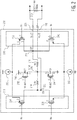
- Fig. 2 depicts a schematic circuit diagram of one embodiment of an LVDS driver circuit 202.
- the LVDS driver circuit depicted in Fig. 2 is an embodiment of the differential driver circuit 102 depicted in Fig. 1 .
- the differential driver circuit depicted in Fig. 1 is not limited to the embodiment depicted in Fig. 2 .
- the LVDS driver circuit 202 includes a current source 230, a current sink 232, a current steering circuit 212 that includes PMOS transistors 234, 236 and NMOS transistors 238, 240, an NMOS transistor “MNSF” 242, a PMOS “MPSF” 244, two resistors 214, 216, and two differential output terminals, "IOP,” 224 and “IOM,” 222.
- the LVDS driver circuit generates differential output signals, "Vout1," "Vout2,” and supplies the differential output signals through the differential output terminals IOP and IOM and corresponding differential lines 226, 228 to a load circuit 210, which may be a 100-ohm resistor or other suitable load circuit.
- the LVDS driver circuit 202 can provide fully matched singled-ended output impedance for high-speed communication.
- the LVDS driver circuit provides the single-ended output impedance to absorb the common mode noise on the differential lines 226, 228.
- common mode noise on differential lines can get reflected multiple times and cause electromagnetic interference that degrades the system performance. Consequently, the LVDS driver circuit can improve the overall system performance.
- the LVDS driver circuit provides perfect matching of output impedances, which absorbs the common mode noise by equal amount. If the output impedances are not identical to each other, common mode noise will get reflected by different magnitude and common mode noise will get converted into differential noise, which increases the bit error rate.
- the LVDS driver circuit can improve the bit-error rate of the communication. Further, the LVDS driver circuit provides differential termination for the load circuit 210. If there is mismatch between differential impedance of transmission media and far end differential termination, there will be differential reflections. Output impedance of driver will help to absorb these reflections and hence improving the bit-error rate.
- the PMOS transistors 234, 236 and the NMOS transistors 238, 240 of the current steering circuit 212 are controlled by complimentary signals, "IN+,” “IN-.,” which can be generated by the complimentary signal generation circuit 104 (depicted in Fig. 1 ).
- gate terminals G of the PMOS transistor 234 and the NMOS transistor 238 are controlled by the digital signal IN+
- gate terminals G of the PMOS transistor 236 and the NMOS transistor 240 are controlled by the digital signal IN-.
- the differential output terminal IOM is connected to drain terminals D of the PMOS transistor 234 and the NMOS transistor 238 and the differential output terminal IOP is connected to drain terminals D of the PMOS transistor 236 and the NMOS transistor 240.
- the current source 230 is connected to source terminals S of the PMOS transistors 234, 236 and the current sink 232 is connected to source terminals S of the NMOS transistors 238, 240.
- the two resistors 214, 216 are connected between the differential output terminals IOP and IOM of the LVDS driver circuit and have identical resistance values, "Rs.”
- the point or node 280 between the two resistors is the node to which the two resistors, the NMOS transistor MNSF and the PMOS transistor MPSF are connected.
- the voltage, "V mid ,” at the point defines the common mode voltage of the LVDS driver output. According to the LVDS standard as defined by IEEE Std 1596.3-1996, the voltage V mid at the point is typically 1.2V.
- transistors MNSF and MPSF are connected as source followers. Specifically, the source terminal S of the NMOS transistor MNSF is connected to the point, and the drain terminal D of the NMOS transistor MNSF is connected to a supply voltage 246. The source terminal S of the PMOS transistor MPSF is also connected to the point, and the drain terminal D of the PMOS transistor MPSF is connected to the ground.
- the gate terminal G of the NMOS transistor MNSF is controlled by a first bias voltage, "V bias1 ,” and the gate terminal G of the PMOS transistor MPSF is controlled by a second bias voltage, “V bias2 .”
- V bias 1 V mid + V th MNSF
- V bias 2 V mid ⁇ V th MPSF
- V th(MNSF) represents the threshold voltage of the NMOS transistor MNSF
- V th(MPSF) represents the absolute value of the threshold voltage of the PMOS transistor MPSF.
- the gate voltage V bias1 of the NMOS transistor MNSF is above the voltage V mid at the point 280 and the gate voltage V bias2 of the PMOS transistor MPSF is lower than the voltage V mid at the point.
- the typical value of the common mode voltage V mid is 1.2V. Consequently, the gate voltage V bias1 of the NMOS transistor MNSF is one transistor threshold above 1.2V and the gate voltage V bias2 of the PMOS transistor MPSF is one transistor threshold lower than 1.2V. Because of the biasing voltage conditions, both the PMOS transistor MPSF and the NMOS transistor MNSF remain almost off when the common mode voltage V mid stays at its typical value of 1.2V.
- the common mode voltage V mid will increase from its typical value of 1.2V.
- the increases of the voltage V mid reduce the gate-to-source voltage of the NMOS transistor MNSF and further turn the NMOS transistor MNSF off, while the gate-to-source voltage of the PMOS transistor MPSF increases, which turns on the PMOS transistor MPSF.
- the output impedances at both the output terminals IOP and IOM are identical to each other when there is a common mode noise of positive magnitude presented on the differential lines.
- the common mode voltage V mid will decrease from its typical value of 1.2V.
- the decreases of the common mode voltage V mid reduces the gate-to-source voltage of the PMOS transistor MPSF and further turns the PMOS transistor MPSF off, while the gate-to-source voltage of the NMOS transistor MNSF increases, which turns on the NMOS transistor MNSF.
- the output impedances of both the output terminals IOP and IOM are identical to each other when there is a common mode noise of negative magnitude presented on the differential lines.
- Values of the output impedances at the output terminals IOP and IOM of the LVDS driver circuit 202 can be decided based on the requirement of the common mode output impedance. For example, if requirement of common mode output impedance is 50 ohm (e.g., to match the common mode impedance of PCB trace), the summation of one of the resistance value R s of the resistor 214 or the resistor 216 and 1/g m of the NMOS transistor MNSF or the PMOS transistor MPSF is 50 ohm.
- the resistance value R s of the resistors can be set to 25 ohm and 1/g m(MNSF) or 1/g m(MPSF) can be set to 25 ohm.
- the resistance value R s of the resistors can be set to 75 ohm and 1/g m(MNSF) and 1/g m(MPSF) can be set to 25-ohm. In this case, if PCB trace impedance is 50 ohm, then 33% of the common mode noise will get reflected and the reflections on both the line will remain same such that it will not get converted into differential noise.
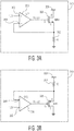
- Fig. 3A depicts an embodiment of a bias voltage generation circuit 306 for generating the bias voltage Vbias1 for the LVDS driver circuit 202 depicted in Fig. 2 .
- the bias voltage generation circuit depicted in Fig. 3A is an embodiment of the first bias voltage generation circuit 106 depicted in Fig. 1 .
- the first bias voltage generation circuit depicted in Fig. 1 is not limited to the embodiment depicted in Fig. 3A .
- the bias voltage generation circuit 306 includes an OP-AMP OP1 350, with one input 352 connected to 1.2V bias voltage, which can be the output of a bandgap circuit.
- the output voltage of the op-amp OP1 is Vbias1, which controls the gate terminal G of an NMOS transistor MN1 356.
- the drain terminal D of the NMOS transistor MN1 is connected to a supply voltage 358 while the source terminal S of the NMOS transistor MN1 is connected to the ground through a resistor R1 359.
- the source terminal S of the NMOS transistor MN1 is also connected to the second input 354 of the op-amp OP1.
- the resistance value of the resistor R1 can be selected such that MN1 is just turned on.
- the voltage Vbias1 is the bias voltage applied to the NMOS transistor MNSF of the LVDS driver circuit depicted in Fig. 2 .
- Fig. 3B depicts an embodiment of a bias voltage generation circuit 308 for generating the bias voltage Vbias2 for the LVDS driver circuit 202 depicted in Fig. 2 .
- the bias voltage generation circuit depicted in Fig. 3B is an embodiment of the second bias voltage generation circuit 108 depicted in Fig. 1 .
- the second bias voltage generation circuit depicted in Fig. 1 is not limited to the embodiment depicted in Fig. 3B .
- the bias voltage generation circuit 308 includes an OP-AMP OP2 360 with one input 362 connected to 1.2V, which can be the output of a bandgap circuit.
- the output voltage of the OP-AMP OP2 is Vbias2, which controls the gate terminal G of a PMOS transistor MP2 366.
- the drain terminal D of the PMOS transistor MP2 is connected to the ground whereas the source terminal S of the PMOS transistor MP2 is connected to a supply voltage 368 through a resistor R2 369.
- the source terminal of the PMOS transistor MP2 is also connected to the second input 364 of the OP-AMP OP2.
- the resistance value of the resistor R2 can be selected such that the PMOS transistor MP2 is just turned on.
- V th(MP2) represents the threshold voltage (absolute value) of the PMOS transistor MP2.
- the voltage Vbias2 is the bias voltage applied to the PMOS transistor MPSF of the LVDS driver circuit depicted in Fig. 2 .
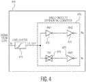
- Fig. 4 depicts an embodiment of a complimentary signal generation circuit 404 that is used to generate complementary digital signals IN+ and IN- for the LVDS driver circuit 202 depicted in Fig. 2 .
- the complimentary signal generation circuit depicted in Fig. 4 is an embodiment of the complimentary signal generation circuit 104 depicted in Fig. 1 .
- the complimentary signal generation depicted in Fig. 1 is not limited to the embodiment depicted in Fig. 4 .
- the complimentary signal generation circuit 404 includes a level shifter 470, inverters INV1 472, INV2 474, INV3 476, and a transmission gate TG1 478.
- the inverters INV1, INV2, INV3 and the transmission gate TG1 form a single-ended-to-differential converter 479.
- the complimentary signal generation circuit Based on the output signal, "LS_OUT," of the level shifter, the complimentary signal generation circuit generates the signal IN+ using two cascaded inverter INV1 and INV2, and generates the signal IN- using the transmission gate TG1 and the inverter INV3.
- the inverters INV2 and INV3 are matched in size and the delay of the transmission gate TG1 is matched with inverter INV1. In these embodiments, symmetrical complementary signal IN+ and IN- with high accuracy can be generated.
- Fig. 5A shows a diagram of simulated values of the output impedances at the output terminals IOP and IOM of the LVDS driver circuit 202 depicted in Fig. 2 versus the voltages at the output terminals IOP and IOM.
- the output impedances at the output terminals IOP and IOM are measured by shorting both the output terminals IOP and IOM and sweep voltage from IV to 1.4V.
- Fig. 5A includes a first plot (at left top) that shows the values of the output impedance at the output terminal IOM (IM_IOM) and a second plot (at left bottom) that shows the values of the output impedance at the output terminal IOP (IM_IOP).
- Fig. 5B shows a diagram of simulated values of the difference between the output impedances at the output terminals IOP and IOM of the LVDS driver circuit depicted in Fig. 2 versus the voltages at the output terminals IOP and IOM.
- the output impedances at the output terminals IOP and IOM are matching across all operating conditions. As shown in Fig. 5B , the difference between the output impedances at the output terminals IOP and IOM is zero across different operating conditions.
- Fig. 6 depicts a circuit 600 for testing the dynamic output impedances and their mismatch at the output terminals IOP and IOM of the LVDS driver circuit 202 depicted in Fig. 2 .
- the circuit includes two resistors 602, 604 with a resistance value Zt, a capacitor 606, and a voltage source 608.
- the circuit is described in LVDS standard IEEE Standard 1596.3-1996. According to LVDS standard IEEE Std 1596.3-1996:
- voltage difference between IOM and IOM should be less than 50mV, which shows the impedance mismatch between the output terminals IOP and IOM is limited to 10%.
- Fig. 7 shows a diagram of waveforms associated with the circuit 600 depicted in Fig. 6 .
- Vnoise represents the waveform 710 of the injected noise
- V IOP represents the waveform 720 of the output voltage at the output terminal IOP
- V IOM represents the waveform 730 of the output voltage at the output terminal IOM
- V IOP-IOM represents the waveform 740 of the difference between the output voltages at the output terminals IOP and IOM.
- the waveforms V IOP and V IOM have a swing that is half of the waveform Vnoise, due to 50-ohm output impedance at IOP and IOM.
- the waveform is close to zero, which shows that there is almost negligible difference between voltages at the output terminals IOP and IOM and proves that the common mode noise is not converted into differential noise.
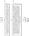
- Fig. 8 depicts a flowchart diagram of one embodiment of a method for controlling a differential driver circuit.
- complimentary signals are applied to a current steering circuit of the differential driver circuit to determine a current direction through differential output terminals of the differential driver circuit.
- different bias voltages are applied to gate terminals of first and second semiconductor circuits of the differential driver circuit. Source terminals of the first and second semiconductor circuits are connected to a point between two resistors of identical resistance values. The two resistors are connected between the differential output terminals of the differential driver circuit and the first and second semiconductor circuits are of different types.
- the differential driver circuit may be the same as or similar to the differential driver circuit 102 depicted in Fig. 1 and/or the LVDS driver circuit 202 depicted in Fig. 2 .
- firmware or software instructions stored on a readable storage medium for execution by a programmable logic device, such as an Application Specific Integrated Circuit (ASIC), a Field Programmable Gate Array (FPGA), a Programmable Logic Chip (PLC), a processor, or the like.
- ASIC Application Specific Integrated Circuit
- FPGA Field Programmable Gate Array
- PLC Programmable Logic Chip
- an embodiment of a program product includes a firmware package stored on a flash memory device and configured to cause an FPGA to perform the operations described herein.
Landscapes
- Engineering & Computer Science (AREA)
- Computer Hardware Design (AREA)
- Physics & Mathematics (AREA)
- Computing Systems (AREA)
- General Engineering & Computer Science (AREA)
- Mathematical Physics (AREA)
- Electromagnetism (AREA)
- General Physics & Mathematics (AREA)
- Radar, Positioning & Navigation (AREA)
- Automation & Control Theory (AREA)
- Dc Digital Transmission (AREA)
- Logic Circuits (AREA)
Claims (10)
- Differentialtreiberschaltung (102) mit:einer Stromlenkschaltung (112), die dazu konfiguriert ist, eine Stromrichtung durch Differentialabgabeanschlüsse der Differentialtreiberschaltung zu bestimmen;zwei Widerständen (214, 216), die zwischen den Differentialabgabeanschlüssen der Differentialtreiberschaltung angeschlossen sind;einem NMOS-Transistor (242) und einem PMOS-Transistor (244); wobeiSource-Anschlüsse des NMOS-Transistors (242) und des PMOS-Transistors (244) mit einem Punkt (280) zwischen den beiden Widerständen verbunden sind;Drain-Anschlüsse des NMOS-Transistors (242) und des PMOS-Transistors (244) mit verschiedenen Versorgungsspannungen verbunden sind;ein Gate-Anschluss des NMOS-Transistors (242) mit einer ersten Bias-Spannung verbunden ist;ein Gate-Anschluss des PMOS-Transistors (244) mit einer zweiten Bias-Spannung verbunden ist; undwobei die erste Bias-Spannung gleich einer Summe einer Referenzspannung und der Schwellwertspannung des NMOS-Transistors (242) ist, die zweite Bias-Spannung gleich einer Spannungsdifferenz zwischen der Referenzspannung und der Schwellwertspannung des PMOS-Transistors (244) ist; und wobei der NMOS-Transistor (242) und der PMOS-Transistor (244) nahezu aus bleiben, wenn die Spannung an dem Punkt (280) zwischen den beiden Widerständen die Referenzspannung ist.
- Differentialtreiberschaltung gemäß Anspruch 1, wobei Widerstandswerte der beiden Widerstände einander identisch sind.
- Differentialtreiberschaltung gemäß einem der vorherigen Ansprüche, wobei eine Differenz zwischen der ersten Bias-Spannung und der zweiten Bias-Spannung gleich einer Summe von Schwellwertspannungen des NMOS-Transistors und des PMOS-Transistors ist.
- Differentialtreiberschaltung gemäß einem der vorherigen Ansprüche, wobei ein Drain-Anschluss des NMOS-Transistors mit einer positiven Versorgungsspannung (246) verbunden ist, und wobei ein Drain-Anschluss des PMOS-Transistors mit der Masse verbunden ist.
- Differentialtreiberschaltung gemäß einem der vorherigen Ansprüche, wobei die Stromlenkschaltung dazu konfiguriert ist, die Stromrichtung durch die Differentialabgabeanschlüsse der Differentialtreiberschaltung auf der Grundlage von komplementären Signalen zu bestimmen.
- Differentialtreiberschaltung gemäß einem der vorherigen Ansprüche, wobei die Stromlenkschaltung (212) einen ersten PMOS-Transistor (234), einen zweiten PMOS-Transistor (236), einen ersten NMOS-Transistor (238) und einen zweiten NMOS-Transistor (240) aufweist, wobei Gate-Anschlüsse des ersten und des zweiten PMOS-Transistors mit den komplementären Signalen (IN+, IN-) verbunden sind, und wobei Gate-Anschlüsse des ersten und des zweiten NMOS-Transistors mit den komplementären Signalen (IN+, IN-) verbunden sind.
- Differentialtreiberschaltung gemäß Anspruch 6, wobei die Differentialabgabeanschlüsse der Differentialtreiberschaltung einen ersten Differentialabgabeanschluss (222) und einen zweiten Differentialabgabeanschluss (224) aufweisen, wobei der erste Differentialabgabeanschluss mit Drain-Anschlüssen des ersten PMOS-Transistors und des ersten NMOS-Transistors verbunden ist, und wobei der zweite Differentialabgabeanschluss mit Drain-Anschlüssen des zweiten PMOS-Transistors und des zweiten NMOS-Transistors verbunden ist.
- Differentialtreiberschaltung gemäß Anspruch 6 oder 7, des Weiteren mit einer Stromquelle (230) und einer Stromsenke (232), wobei die Stromquelle mit Source-Anschlüssen des ersten und des zweiten PMOS-Transistors verbunden ist, und wobei die Stromsenke mit Source-Anschlüssen des ersten und des zweiten NMOS-Transistors verbunden ist.
- Differentialtreiberschaltung gemäß einem der vorherigen Ansprüche, wobei die Differentialtreiberschaltung eine Low-Voltage-Differential-Signaling- (LVDS-) Treiberschaltung ist.
- Differentialtreibersystem mit der Differentialtreiberschaltung gemäß einem der vorherigen Ansprüche, einer Komplementärsignalerzeugungsschaltung, die dazu konfiguriert ist, komplementäre Signale für die Differentialtreiberschaltung zu erzeugen, und einer Mehrzahl von Biasspannungserzeugungsschaltungen, die dazu konfiguriert sind, Biasspannungen für die Differentialtreiberschaltung zu erzeugen.
Applications Claiming Priority (1)
| Application Number | Priority Date | Filing Date | Title |
|---|---|---|---|
| US14/875,582 US9391602B1 (en) | 2015-10-05 | 2015-10-05 | Differential driver circuit and method for controlling a differential driver circuit |
Publications (2)
| Publication Number | Publication Date |
|---|---|
| EP3154201A1 EP3154201A1 (de) | 2017-04-12 |
| EP3154201B1 true EP3154201B1 (de) | 2019-10-23 |
Family
ID=56321165
Family Applications (1)
| Application Number | Title | Priority Date | Filing Date |
|---|---|---|---|
| EP16192243.0A Active EP3154201B1 (de) | 2015-10-05 | 2016-10-04 | Differentialtreiberschaltung und verfahren zur steuerung einer differentialtreiberschaltung |
Country Status (3)
| Country | Link |
|---|---|
| US (1) | US9391602B1 (de) |
| EP (1) | EP3154201B1 (de) |
| CN (1) | CN106843349B (de) |
Families Citing this family (6)
| Publication number | Priority date | Publication date | Assignee | Title |
|---|---|---|---|---|
| US10514742B2 (en) * | 2017-12-28 | 2019-12-24 | Nxp B.V. | Power down signal generating circuit |
| US10812067B1 (en) * | 2019-06-07 | 2020-10-20 | Nxp B.V. | Redriver and resistive unit for a redriver |
| CN113810042B (zh) * | 2020-06-16 | 2025-08-01 | 恩智浦美国有限公司 | 低压差分信号驱动器 |
| CN113992239B (zh) * | 2021-12-24 | 2022-03-18 | 长芯盛(武汉)科技有限公司 | 一种用于对高速差分信号进行检测的装置及其方法 |
| US12212318B2 (en) * | 2022-02-28 | 2025-01-28 | Stmicroelectronics International N.V. | Low-voltage differential signaling (LVDS) transmitter circuit |
| CN119182392A (zh) * | 2023-06-21 | 2024-12-24 | 澜起电子科技(上海)有限公司 | 输出驱动电路、时钟芯片及电子设备 |
Family Cites Families (19)
| Publication number | Priority date | Publication date | Assignee | Title |
|---|---|---|---|---|
| US6107859A (en) * | 1997-12-12 | 2000-08-22 | Cypress Semiconductor Corp. | Low power buffer circuit and method for generating a common-mode output absent process-induced mismatch error |
| US5939904A (en) * | 1998-02-19 | 1999-08-17 | Lucent Technologies, Inc. | Method and apparatus for controlling the common-mode output voltage of a differential buffer |
| JP3415508B2 (ja) * | 1999-09-27 | 2003-06-09 | エヌイーシーマイクロシステム株式会社 | ドライバ回路及びその出力安定化方法 |
| US6847232B2 (en) | 2001-11-08 | 2005-01-25 | Texas Instruments Incorporated | Interchangeable CML/LVDS data transmission circuit |
| US6943588B1 (en) * | 2003-09-24 | 2005-09-13 | Altera Corporation | Dynamically-adjustable differential output drivers |
| EP1743424A1 (de) | 2004-04-20 | 2007-01-17 | Koninklijke Philips Electronics N.V. | Ac-kopplung und gate-ladungspumpen für die nmos- und pmos-bauelementesteuerung |
| US7236018B1 (en) * | 2004-09-08 | 2007-06-26 | Altera Corporation | Programmable low-voltage differential signaling output driver |
| US20060066393A1 (en) | 2004-09-30 | 2006-03-30 | Bradley Kendall Davis | High-speed, low-power, low-skew, low-voltage differential receiver |
| US7598779B1 (en) * | 2004-10-08 | 2009-10-06 | Altera Corporation | Dual-mode LVDS/CML transmitter methods and apparatus |
| CN100488053C (zh) * | 2005-09-05 | 2009-05-13 | 中兴通讯股份有限公司 | 一种低压差分信号驱动器电路 |
| EP2002623A1 (de) | 2006-03-27 | 2008-12-17 | Nxp B.V. | Niederspannungs- und niederstromdifferenzialtreiber mit abgestimmten ausgangsimpedanzen |
| JP4858959B2 (ja) * | 2006-06-06 | 2012-01-18 | ルネサスエレクトロニクス株式会社 | 差動信号駆動回路及び差動信号駆動方法 |
| US7911244B2 (en) * | 2007-11-30 | 2011-03-22 | Sony Corporation | Differential drive circuit and communication device |
| US7961014B2 (en) | 2009-10-26 | 2011-06-14 | Analog Devices, Inc. | Apparatus and method for providing multi-mode clock signals |
| US8049534B2 (en) * | 2010-02-15 | 2011-11-01 | Texas Instruments Incorporated | Low-power high-speed differential driver with precision current steering |
| US8415979B2 (en) * | 2010-11-04 | 2013-04-09 | Mediatek Inc. | Differential driver with calibration circuit and related calibration method |
| CN103427823B (zh) * | 2012-05-23 | 2016-04-13 | 上海华虹宏力半导体制造有限公司 | 低电压差分信号传输驱动器电路 |
| JP6140573B2 (ja) * | 2012-09-03 | 2017-05-31 | 株式会社メガチップス | 出力バッファ回路 |
| CN204481788U (zh) * | 2015-04-07 | 2015-07-15 | 电子科技大学 | 一种可抑制输出共模波动的lvds驱动电路 |
-
2015
- 2015-10-05 US US14/875,582 patent/US9391602B1/en active Active
-
2016
- 2016-09-30 CN CN201610871789.7A patent/CN106843349B/zh active Active
- 2016-10-04 EP EP16192243.0A patent/EP3154201B1/de active Active
Non-Patent Citations (1)
| Title |
|---|
| None * |
Also Published As
| Publication number | Publication date |
|---|---|
| CN106843349B (zh) | 2020-07-03 |
| CN106843349A (zh) | 2017-06-13 |
| EP3154201A1 (de) | 2017-04-12 |
| US9391602B1 (en) | 2016-07-12 |
Similar Documents
| Publication | Publication Date | Title |
|---|---|---|
| EP3154201B1 (de) | Differentialtreiberschaltung und verfahren zur steuerung einer differentialtreiberschaltung | |
| US8415986B2 (en) | Voltage-mode driver with pre-emphasis | |
| US7893720B2 (en) | Bus low voltage differential signaling (BLVDS) circuit | |
| US6294932B1 (en) | Input circuit, output circuit, input-output circuit and method of processing input signals | |
| US8198912B1 (en) | Driver circuit correction arm decoupling resistance in steady state mode | |
| US20180083628A1 (en) | Signal processing devices and methods | |
| EP1548944B1 (de) | Empfangsvorrichtung | |
| US20070124518A1 (en) | Transmitter driver circuit in high-speed serial communications system | |
| CN109787611B (zh) | 一种适用于电平转换芯片的自选择偏置电路 | |
| US20150155875A1 (en) | Lvds driver | |
| JP7049826B2 (ja) | 送信回路及び該送信回路の制御方法 | |
| US8441281B2 (en) | Current-mode logic buffer with enhanced output swing | |
| US9941958B2 (en) | On-chip test interface for voltage-mode Mach-Zehnder modulator driver | |
| US10135442B2 (en) | Current-mode logic circuit | |
| US11290073B1 (en) | Self-biased differential transmitter | |
| US11128496B2 (en) | Transmitter with equalization | |
| US20130241602A1 (en) | Transmission circuit | |
| US11005477B2 (en) | Driver circuit and control method therefor, and transmission/reception system | |
| CN109450436B (zh) | 一种信号传输管的驱动电路和电平转换电路 | |
| US20230231476A1 (en) | Driver circuit for low voltage differential signaling, lvds, line driver arrangement for lvds and method for operating an lvds driver circuit | |
| JP2015091092A (ja) | ドライバ回路および半導体集積回路装置 | |
| US11515876B2 (en) | Driver for a shared bus, in particular a LIN bus | |
| US9847777B2 (en) | Signal potential converter | |
| JP2007068169A (ja) | 信号伝送装置及び信号伝送方法 | |
| CN100579188C (zh) | 电流模式接口接收器及其运作方法 |
Legal Events
| Date | Code | Title | Description |
|---|---|---|---|
| PUAI | Public reference made under article 153(3) epc to a published international application that has entered the european phase |
Free format text: ORIGINAL CODE: 0009012 |
|
| STAA | Information on the status of an ep patent application or granted ep patent |
Free format text: STATUS: THE APPLICATION HAS BEEN PUBLISHED |
|
| AK | Designated contracting states |
Kind code of ref document: A1 Designated state(s): AL AT BE BG CH CY CZ DE DK EE ES FI FR GB GR HR HU IE IS IT LI LT LU LV MC MK MT NL NO PL PT RO RS SE SI SK SM TR |
|
| AX | Request for extension of the european patent |
Extension state: BA ME |
|
| STAA | Information on the status of an ep patent application or granted ep patent |
Free format text: STATUS: REQUEST FOR EXAMINATION WAS MADE |
|
| 17P | Request for examination filed |
Effective date: 20171012 |
|
| RBV | Designated contracting states (corrected) |
Designated state(s): AL AT BE BG CH CY CZ DE DK EE ES FI FR GB GR HR HU IE IS IT LI LT LU LV MC MK MT NL NO PL PT RO RS SE SI SK SM TR |
|
| STAA | Information on the status of an ep patent application or granted ep patent |
Free format text: STATUS: EXAMINATION IS IN PROGRESS |
|
| 17Q | First examination report despatched |
Effective date: 20181024 |
|
| GRAP | Despatch of communication of intention to grant a patent |
Free format text: ORIGINAL CODE: EPIDOSNIGR1 |
|
| STAA | Information on the status of an ep patent application or granted ep patent |
Free format text: STATUS: GRANT OF PATENT IS INTENDED |
|
| INTG | Intention to grant announced |
Effective date: 20190527 |
|
| GRAS | Grant fee paid |
Free format text: ORIGINAL CODE: EPIDOSNIGR3 |
|
| GRAA | (expected) grant |
Free format text: ORIGINAL CODE: 0009210 |
|
| STAA | Information on the status of an ep patent application or granted ep patent |
Free format text: STATUS: THE PATENT HAS BEEN GRANTED |
|
| AK | Designated contracting states |
Kind code of ref document: B1 Designated state(s): AL AT BE BG CH CY CZ DE DK EE ES FI FR GB GR HR HU IE IS IT LI LT LU LV MC MK MT NL NO PL PT RO RS SE SI SK SM TR |
|
| REG | Reference to a national code |
Ref country code: GB Ref legal event code: FG4D |
|
| REG | Reference to a national code |
Ref country code: CH Ref legal event code: EP |
|
| REG | Reference to a national code |
Ref country code: IE Ref legal event code: FG4D |
|
| REG | Reference to a national code |
Ref country code: DE Ref legal event code: R096 Ref document number: 602016022830 Country of ref document: DE |
|
| REG | Reference to a national code |
Ref country code: AT Ref legal event code: REF Ref document number: 1194836 Country of ref document: AT Kind code of ref document: T Effective date: 20191115 |
|
| REG | Reference to a national code |
Ref country code: NL Ref legal event code: MP Effective date: 20191023 |
|
| REG | Reference to a national code |
Ref country code: LT Ref legal event code: MG4D |
|
| PG25 | Lapsed in a contracting state [announced via postgrant information from national office to epo] |
Ref country code: PL Free format text: LAPSE BECAUSE OF FAILURE TO SUBMIT A TRANSLATION OF THE DESCRIPTION OR TO PAY THE FEE WITHIN THE PRESCRIBED TIME-LIMIT Effective date: 20191023 Ref country code: LT Free format text: LAPSE BECAUSE OF FAILURE TO SUBMIT A TRANSLATION OF THE DESCRIPTION OR TO PAY THE FEE WITHIN THE PRESCRIBED TIME-LIMIT Effective date: 20191023 Ref country code: GR Free format text: LAPSE BECAUSE OF FAILURE TO SUBMIT A TRANSLATION OF THE DESCRIPTION OR TO PAY THE FEE WITHIN THE PRESCRIBED TIME-LIMIT Effective date: 20200124 Ref country code: NO Free format text: LAPSE BECAUSE OF FAILURE TO SUBMIT A TRANSLATION OF THE DESCRIPTION OR TO PAY THE FEE WITHIN THE PRESCRIBED TIME-LIMIT Effective date: 20200123 Ref country code: NL Free format text: LAPSE BECAUSE OF FAILURE TO SUBMIT A TRANSLATION OF THE DESCRIPTION OR TO PAY THE FEE WITHIN THE PRESCRIBED TIME-LIMIT Effective date: 20191023 Ref country code: FI Free format text: LAPSE BECAUSE OF FAILURE TO SUBMIT A TRANSLATION OF THE DESCRIPTION OR TO PAY THE FEE WITHIN THE PRESCRIBED TIME-LIMIT Effective date: 20191023 Ref country code: BG Free format text: LAPSE BECAUSE OF FAILURE TO SUBMIT A TRANSLATION OF THE DESCRIPTION OR TO PAY THE FEE WITHIN THE PRESCRIBED TIME-LIMIT Effective date: 20200123 Ref country code: PT Free format text: LAPSE BECAUSE OF FAILURE TO SUBMIT A TRANSLATION OF THE DESCRIPTION OR TO PAY THE FEE WITHIN THE PRESCRIBED TIME-LIMIT Effective date: 20200224 Ref country code: LV Free format text: LAPSE BECAUSE OF FAILURE TO SUBMIT A TRANSLATION OF THE DESCRIPTION OR TO PAY THE FEE WITHIN THE PRESCRIBED TIME-LIMIT Effective date: 20191023 Ref country code: SE Free format text: LAPSE BECAUSE OF FAILURE TO SUBMIT A TRANSLATION OF THE DESCRIPTION OR TO PAY THE FEE WITHIN THE PRESCRIBED TIME-LIMIT Effective date: 20191023 |
|
| PG25 | Lapsed in a contracting state [announced via postgrant information from national office to epo] |
Ref country code: HR Free format text: LAPSE BECAUSE OF FAILURE TO SUBMIT A TRANSLATION OF THE DESCRIPTION OR TO PAY THE FEE WITHIN THE PRESCRIBED TIME-LIMIT Effective date: 20191023 Ref country code: RS Free format text: LAPSE BECAUSE OF FAILURE TO SUBMIT A TRANSLATION OF THE DESCRIPTION OR TO PAY THE FEE WITHIN THE PRESCRIBED TIME-LIMIT Effective date: 20191023 Ref country code: IS Free format text: LAPSE BECAUSE OF FAILURE TO SUBMIT A TRANSLATION OF THE DESCRIPTION OR TO PAY THE FEE WITHIN THE PRESCRIBED TIME-LIMIT Effective date: 20200224 |
|
| PG25 | Lapsed in a contracting state [announced via postgrant information from national office to epo] |
Ref country code: AL Free format text: LAPSE BECAUSE OF FAILURE TO SUBMIT A TRANSLATION OF THE DESCRIPTION OR TO PAY THE FEE WITHIN THE PRESCRIBED TIME-LIMIT Effective date: 20191023 |
|
| REG | Reference to a national code |
Ref country code: DE Ref legal event code: R097 Ref document number: 602016022830 Country of ref document: DE |
|
| PG2D | Information on lapse in contracting state deleted |
Ref country code: IS |
|
| PG25 | Lapsed in a contracting state [announced via postgrant information from national office to epo] |
Ref country code: ES Free format text: LAPSE BECAUSE OF FAILURE TO SUBMIT A TRANSLATION OF THE DESCRIPTION OR TO PAY THE FEE WITHIN THE PRESCRIBED TIME-LIMIT Effective date: 20191023 Ref country code: CZ Free format text: LAPSE BECAUSE OF FAILURE TO SUBMIT A TRANSLATION OF THE DESCRIPTION OR TO PAY THE FEE WITHIN THE PRESCRIBED TIME-LIMIT Effective date: 20191023 Ref country code: EE Free format text: LAPSE BECAUSE OF FAILURE TO SUBMIT A TRANSLATION OF THE DESCRIPTION OR TO PAY THE FEE WITHIN THE PRESCRIBED TIME-LIMIT Effective date: 20191023 Ref country code: DK Free format text: LAPSE BECAUSE OF FAILURE TO SUBMIT A TRANSLATION OF THE DESCRIPTION OR TO PAY THE FEE WITHIN THE PRESCRIBED TIME-LIMIT Effective date: 20191023 Ref country code: RO Free format text: LAPSE BECAUSE OF FAILURE TO SUBMIT A TRANSLATION OF THE DESCRIPTION OR TO PAY THE FEE WITHIN THE PRESCRIBED TIME-LIMIT Effective date: 20191023 Ref country code: IS Free format text: LAPSE BECAUSE OF FAILURE TO SUBMIT A TRANSLATION OF THE DESCRIPTION OR TO PAY THE FEE WITHIN THE PRESCRIBED TIME-LIMIT Effective date: 20200223 |
|
| REG | Reference to a national code |
Ref country code: AT Ref legal event code: MK05 Ref document number: 1194836 Country of ref document: AT Kind code of ref document: T Effective date: 20191023 |
|
| PLBE | No opposition filed within time limit |
Free format text: ORIGINAL CODE: 0009261 |
|
| STAA | Information on the status of an ep patent application or granted ep patent |
Free format text: STATUS: NO OPPOSITION FILED WITHIN TIME LIMIT |
|
| PG25 | Lapsed in a contracting state [announced via postgrant information from national office to epo] |
Ref country code: SK Free format text: LAPSE BECAUSE OF FAILURE TO SUBMIT A TRANSLATION OF THE DESCRIPTION OR TO PAY THE FEE WITHIN THE PRESCRIBED TIME-LIMIT Effective date: 20191023 Ref country code: IT Free format text: LAPSE BECAUSE OF FAILURE TO SUBMIT A TRANSLATION OF THE DESCRIPTION OR TO PAY THE FEE WITHIN THE PRESCRIBED TIME-LIMIT Effective date: 20191023 Ref country code: SM Free format text: LAPSE BECAUSE OF FAILURE TO SUBMIT A TRANSLATION OF THE DESCRIPTION OR TO PAY THE FEE WITHIN THE PRESCRIBED TIME-LIMIT Effective date: 20191023 |
|
| 26N | No opposition filed |
Effective date: 20200724 |
|
| PG25 | Lapsed in a contracting state [announced via postgrant information from national office to epo] |
Ref country code: AT Free format text: LAPSE BECAUSE OF FAILURE TO SUBMIT A TRANSLATION OF THE DESCRIPTION OR TO PAY THE FEE WITHIN THE PRESCRIBED TIME-LIMIT Effective date: 20191023 Ref country code: SI Free format text: LAPSE BECAUSE OF FAILURE TO SUBMIT A TRANSLATION OF THE DESCRIPTION OR TO PAY THE FEE WITHIN THE PRESCRIBED TIME-LIMIT Effective date: 20191023 |
|
| REG | Reference to a national code |
Ref country code: CH Ref legal event code: PL |
|
| GBPC | Gb: european patent ceased through non-payment of renewal fee |
Effective date: 20201004 |
|
| PG25 | Lapsed in a contracting state [announced via postgrant information from national office to epo] |
Ref country code: MC Free format text: LAPSE BECAUSE OF FAILURE TO SUBMIT A TRANSLATION OF THE DESCRIPTION OR TO PAY THE FEE WITHIN THE PRESCRIBED TIME-LIMIT Effective date: 20191023 Ref country code: LU Free format text: LAPSE BECAUSE OF NON-PAYMENT OF DUE FEES Effective date: 20201004 |
|
| REG | Reference to a national code |
Ref country code: BE Ref legal event code: MM Effective date: 20201031 |
|
| PG25 | Lapsed in a contracting state [announced via postgrant information from national office to epo] |
Ref country code: CH Free format text: LAPSE BECAUSE OF NON-PAYMENT OF DUE FEES Effective date: 20201031 Ref country code: BE Free format text: LAPSE BECAUSE OF NON-PAYMENT OF DUE FEES Effective date: 20201031 Ref country code: LI Free format text: LAPSE BECAUSE OF NON-PAYMENT OF DUE FEES Effective date: 20201031 Ref country code: GB Free format text: LAPSE BECAUSE OF NON-PAYMENT OF DUE FEES Effective date: 20201004 |
|
| PG25 | Lapsed in a contracting state [announced via postgrant information from national office to epo] |
Ref country code: IE Free format text: LAPSE BECAUSE OF NON-PAYMENT OF DUE FEES Effective date: 20201004 |
|
| PG25 | Lapsed in a contracting state [announced via postgrant information from national office to epo] |
Ref country code: TR Free format text: LAPSE BECAUSE OF FAILURE TO SUBMIT A TRANSLATION OF THE DESCRIPTION OR TO PAY THE FEE WITHIN THE PRESCRIBED TIME-LIMIT Effective date: 20191023 Ref country code: MT Free format text: LAPSE BECAUSE OF FAILURE TO SUBMIT A TRANSLATION OF THE DESCRIPTION OR TO PAY THE FEE WITHIN THE PRESCRIBED TIME-LIMIT Effective date: 20191023 Ref country code: CY Free format text: LAPSE BECAUSE OF FAILURE TO SUBMIT A TRANSLATION OF THE DESCRIPTION OR TO PAY THE FEE WITHIN THE PRESCRIBED TIME-LIMIT Effective date: 20191023 |
|
| PG25 | Lapsed in a contracting state [announced via postgrant information from national office to epo] |
Ref country code: MK Free format text: LAPSE BECAUSE OF FAILURE TO SUBMIT A TRANSLATION OF THE DESCRIPTION OR TO PAY THE FEE WITHIN THE PRESCRIBED TIME-LIMIT Effective date: 20191023 |
|
| P01 | Opt-out of the competence of the unified patent court (upc) registered |
Effective date: 20230725 |
|
| PGFP | Annual fee paid to national office [announced via postgrant information from national office to epo] |
Ref country code: FR Payment date: 20250924 Year of fee payment: 10 |
|
| PGFP | Annual fee paid to national office [announced via postgrant information from national office to epo] |
Ref country code: DE Payment date: 20250923 Year of fee payment: 10 |