EP3152670B1 - Ice pin functionality for multi-processor core devices - Google Patents
Ice pin functionality for multi-processor core devices Download PDFInfo
- Publication number
- EP3152670B1 EP3152670B1 EP15731175.4A EP15731175A EP3152670B1 EP 3152670 B1 EP3152670 B1 EP 3152670B1 EP 15731175 A EP15731175 A EP 15731175A EP 3152670 B1 EP3152670 B1 EP 3152670B1
- Authority
- EP
- European Patent Office
- Prior art keywords
- pin
- peripheral
- ownership
- microcontrollers
- embedded device
- Prior art date
- Legal status (The legal status is an assumption and is not a legal conclusion. Google has not performed a legal analysis and makes no representation as to the accuracy of the status listed.)
- Active
Links
Images

Classifications
-
- G—PHYSICS
- G06—COMPUTING OR CALCULATING; COUNTING
- G06F—ELECTRIC DIGITAL DATA PROCESSING
- G06F1/00—Details not covered by groups G06F3/00 - G06F13/00 and G06F21/00
- G06F1/22—Means for limiting or controlling the pin/gate ratio
-
- G—PHYSICS
- G06—COMPUTING OR CALCULATING; COUNTING
- G06F—ELECTRIC DIGITAL DATA PROCESSING
- G06F13/00—Interconnection of, or transfer of information or other signals between, memories, input/output devices or central processing units
- G06F13/14—Handling requests for interconnection or transfer
- G06F13/20—Handling requests for interconnection or transfer for access to input/output bus
- G06F13/28—Handling requests for interconnection or transfer for access to input/output bus using burst mode transfer, e.g. direct memory access DMA, cycle steal
- G06F13/287—Multiplexed DMA
-
- G—PHYSICS
- G06—COMPUTING OR CALCULATING; COUNTING
- G06F—ELECTRIC DIGITAL DATA PROCESSING
- G06F13/00—Interconnection of, or transfer of information or other signals between, memories, input/output devices or central processing units
- G06F13/38—Information transfer, e.g. on bus
- G06F13/382—Information transfer, e.g. on bus using universal interface adapter
- G06F13/385—Information transfer, e.g. on bus using universal interface adapter for adaptation of a particular data processing system to different peripheral devices
-
- G—PHYSICS
- G06—COMPUTING OR CALCULATING; COUNTING
- G06F—ELECTRIC DIGITAL DATA PROCESSING
- G06F15/00—Digital computers in general; Data processing equipment in general
- G06F15/76—Architectures of general purpose stored program computers
Definitions
- the present disclosure relates to multi-processor core devices, in particular multi-processor core microcontrollers.
- a microcontroller is a system on a chip and comprises not only a central processing unit (CPU), but also memory, I/O ports, and a plurality of peripherals.
- a multi-processor core device such as a multi-core microcontroller, comprises not only one CPU but two or more central processing cores. Such a device provides increased performance, improved security, and aiding software development. In embedded devices, these devices require to use a housing with a high number of pins.
- Multi-core devices are designed for symmetrical multi-processor core operation where the processor cores are designed not to be “different” in function or purpose. Such systems have no need to have one specific processor core to have control of a specific device pin. Other devices that have asymmetrical multi-processor core typically use the other "core(s)" as dedicated functions such as floating point which do not need access to device pins.
- US Patent Application Publication US2013/0067259 discloses a standby operation with additional micro-controller.
- Reference data sheet DS70190E “Section 30. I/O Ports with Peripheral Pin Select (PPS)", published by Microchip in 2012, pages 30-1 to 30-37 , discloses a peripheral pin select module for microcontrollers.
- Data Sheet “ F28M36x ConcertoTM Microcontrollers”, Texas Instruments, Feb. 2014 discloses a device with a master and a control subsystem which share external pins among internal peripherals.
- an embedded device may comprise a plurality of processor cores, each comprising a plurality of peripheral devices, wherein each peripheral device may comprise an output; a housing comprising a plurality of assignable external pins; and a plurality of peripheral pin selection modules for each processing core, wherein each peripheral pin selection module is configured to be programmable to assign an assignable external pin to one of the plurality of peripheral devices of one of the processor cores.
- each peripheral pin selection module can be programmable only by the associated processing core.
- each peripheral pin selection module may comprise a multiplexer providing an output signal for a single external pin and a plurality of inputs coupled with outputs of peripheral devices of a single processing core.
- each processing core may comprise memory that cannot be accessed by other processing cores.
- the memory may comprise flash memory and random access memory (RAM).
- each peripheral pin selection module may be controlled by a special function register.
- the special function register may be memory mapped into the RAM.
- each processing core may have a number of external pins assigned to it exclusively.
- the embedded device may further comprise ownership logic programmable to assign an external pin to any of the plurality of processing cores.
- ownership of an external pin can be programmed into configuration bits stored into flash memory.
- a method for selecting output functionality of external pins in an embedded device may comprise the steps of: arranging a plurality of processor cores and an associated plurality of peripheral devices on a single chip within a housing having a plurality of external pins, wherein each peripheral device may comprise an output; arranging a plurality of peripheral pin selection modules for each processing core on said single chip, and programming at least one of the peripheral pin selection modules by an associated processing core to couple an assignable external pin to one of the plurality of peripheral devices of the respective processing core.
- each peripheral pin selection module is programmable only by the associated processing core.
- each peripheral pin selection module may comprise a multiplexer providing an output signal for a single external pin and a plurality of inputs coupled with outputs of peripheral devices of a single processing core.
- each processing core may comprise memory that cannot be accessed by other processing cores.
- the memory may comprise flash memory and random access memory (RAM).
- the method may further comprise the step of controlling each peripheral pin selection module by a special function register.
- the method may further comprise the step of memory mapping the special function register into the RAM.
- each processing core may have a number of external pins assigned to it exclusively.
- the method may further comprise the step of providing ownership logic programmable to assign an external pin to any of the plurality of processing cores.
- the method may further comprise the step of programming ownership data of an external pin into configuration bits stored into flash memory.
- a limited number of device pins can be assigned to each processor's peripheral(s) in the device while maintaining application flexibility, and provide protection from inadvertent interference from one processor to affecting the functionality of another processor's device pin(s).
- a Peripheral Pin Select (PPS) function module allows to assign variably certain external pins to internal functions.
- the PPS module is implemented for each functional pin in the device for each processor on the device.
- a multi-processor microcontroller can be designed that can be arranged in a housing having less pins than a bus width of each of the processing cores.
- a 28 pin housing may comprise for example a dual core microcontroller wherein each core is a 32 bit microprocessor core.
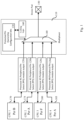
- FIG. 1 shows an embodiment of a single chip microcontroller with, for example, four processor cores (not shown in Fig. 1 ).
- a plurality but limited number of assignable external pins 150 are provided.
- such a device may of course have certain fixed function pins whose function cannot be altered, such as, for example, power supply pins.
- Each processor core is associated with its own peripheral pin select (PPS) module 120a, b, c, d for each external assignable pin.
- PPS peripheral pin select
- Each PPS module 1 10a, b, c, d comprises logic 110 for each processor for each functional device pin 150 (only one per processing core shown in Fig. 1 ).
- POL Pin Ownership Logic
- the logic may for example comprise a configuration register 130 that controls a multiplexer 140 that selects the outputs of the peripheral chosen to drive a device pin 150.
- the output selection is replicated so that other circuitry can decide which processor's peripheral actually gains access to the respective device pin 150.
- FIG. 1 shows four exemplary peripheral devices, wherein each is owned by one of four processing cores.
- each processing core may comprise a plurality of peripheral devices or modules.
- Peripheral devices may have input and/or output functionality. While inputs may be routed to various peripherals, even peripherals associated with different processing cores, only one output functionality of one selected peripherals device can be assigned to an external pin as otherwise a collision or conflict would occur.
- An I/O port associated with a processing core may be considered as a peripheral device or module according to various embodiments and its output functionality is therefore assignable to an external pin.
- the first peripheral 170 is associated with CPU 1
- the second peripheral 175 is associated with CPU 2
- the third peripheral 180 is associated with CPU 3
- the fourth peripheral is associated with CPU 4.
- Respective peripheral pin select modules 120a, b, c, d are programmed to select one of a plurality of peripherals.
- Fig. 1 only shows the selected peripheral.
- each PPS module 120 is designed to actually select a peripheral device or module from its pool of peripherals, each PPS module 120 may be connected to a plurality of peripheral devices or modules of an associated CPU as will be explained with respect to Fig. 2 in more detail.
- FIG. 1 further shows with the indicated block 110 a typical instance of the POL (Pin Ownership Logic) logic that is associated with each functional pin 150 in the device.
- POL Packe Ownership Logic
- Each pin 150 has a multiplexer 140 controlled by configuration bits 130 located, in protected memory (i.e., flash memory). These configuration bits 130 are programmed by the user to specify which processor has access to outputting on a specific device pin 150.
- the configuration bits 130 control respective multiplexers 140 that select the data from a preselected peripheral owned by the selected processor.
- This POL block 110 is replicated for each functional device pin.
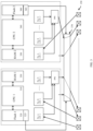
- FIG. 2 shows another diagram of an embodiment of a typical PPS module 120. It shows an exemplary logic within a single PPS module.
- Each processor may own one or more peripheral devices 210, 220, 230, 240. Some or all of these peripheral devices may be coupled with a multiplexer 260 that is controlled by a register 250. According to some embodiments, register 250 is private to the respective processor that owns the peripherals.
- the output 270 of multiplexer 260 is coupled with the multi-processor core pin ownership logic 110.
- an embedded system comprising a multi- processor core can be designed for very low pin count packages, for example a 28-pin housing may be used for microcontroller with a dual core.
- a mechanism is provided according to various embodiments to allow a user to assign peripheral pin functionality.
- a methodology can be provided that enables each processor core in an asymmetrical multi-processor core device to specify which of its peripheral functions are connected to a functional device pin.
- asymmetrical means that each processing core may have different peripheral devices associated with it, wherein certain peripherals may be unique to only one core and others may be embedded in more than one or all cores.
- each processor in a multi-core device has: A PPS multiplexer 260 for each pin.
- Each PPS multiplexer has registers 250 that specify the peripheral connections to the device pin.
- Register 250 can be a special function register that can only be accessed by one processing core, namely the owner of the respective peripherals.
- the special function register 250 may be preferably memory mapped to the random access memory (RAM). This special function register may otherwise operate similar to the configuration register controlling the ownership as explained below.
- pin ownership configuration bits 130 associated with each device pin 150 are located preferably in Flash and/or RAM memory according to various embodiments. These pin ownership configuration bits 130 may control which processor core has authority to output a signal on each device pin 150. For example, such a register may have four bits in a 4 processing core device. Internal control logic may allow that only one bit is set at a time. For example, the setting of one bit may automatically clear all other bits. Other mechanisms may be possible, for example, a two bit register may be used wherein a stored value represents an association with a respective core. If a configuration register has more bits than needed, then invalid settings would simply assign a respective pin to no specific processor. Such a pin could then be used for input only.
- All processor cores may use a device pin for input functions at the same time, but the ability to output a signal on a specific device pin is specific by the customer via the Pin ownership configuration bits 130.
- each functional device pin has:
- the flash memory comprises write lock logic which prevents accidental pin configuration changes.
- the user configures the pin ownership bits during programming. Thus, the pin ownership can only be changed during the programming and cannot be changed dynamically under program control.
- the pin configuration info is transferred to the MUX control.
- control software may further include routines that allow a change of assignments only if, for example, a locking mechanism 160 as, for example, shown in Fig. 1 is not activated for a pin. Thus, a re-assignment of certain pins can be blocked. Thus, a pin may be only re-assignable if a certain task by one processor core has been finished.
- such a blocking function may be established in an associated control register 160.
- a plurality of bits may indicate for which processor core the blocking function is provided.
- only the assigned processor core for which the blocking function has been activated may be able to reset the blocking function.
- the blocking of a pin assignment may only be lifted by the processor for the pin is currently assigned.
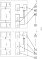
- Fig. 3 shows a block diagram of an embodiment of a dual core microcontroller in a single housing.
- the device comprises basically two separate processing cores 310 and 340 each having a plurality of associated peripheral devices and its own memory.
- the processing cores may have a Harvard structure with separate program memory, e.g., flash memory and data memory. However, other architecture may apply. With respect to these elements, the microcontroller do not share any of their resources.
- the integrated circuit device thus, comprises basically two separate microcontrollers each comprising a CPU 310, 340, flash memory 320, 360, random access memory 330, 350 and a plurality of peripheral devices or modules (Per. A, Per B ... Per N) associated with the respective CPU 310 or 340.
- each processing core 310, 320 may be controlled through respective special function registers which can be preferably memory mapped to the respective RAM 330 and 360.
- the PPS control register 250 as shown in Fig. 2 can be memory mapped to the RAM.
- the flash memory may include configuration registers 325 and 365, respectively, which may control the setting of the PPO module 370.
- PPO module is shown in Fig. 3 as one block and may contain a plurality of PPO units each responsible for a single external pin.
- Fig. 3 indicates an exemplary setting programmed into unit 370 by dotted lines connecting the outputs of certain peripherals with some of the external pins 150 according to a setting of the configuration bits in flash memory 325 and 365.
- other configuration methods may apply, such as volatile or non-volatile registers arranged in RAM or separately from the main memory.
- Fig. 4 shows an embodiment without the protected pin ownership modules 110.
- a predefined number for example, 50% of available assignable external pins 150 are assigned to the first processing core 310 and the remaining 50% to the second processing core 340.
- Each processing core can assign output functionality to any of its peripherals within the respective group of external pins. 150. Again, input functionality can be provided to multiple peripherals even peripherals that are not owned by a single processing core.
- Fig. 4 shows only a single PPS. However, any external pin designated to provide an output function has an associated PPS. Also, in some embodiments, each processing core may have a different number of PPS and not all external pins may be available for each processing core.
Landscapes
- Engineering & Computer Science (AREA)
- Theoretical Computer Science (AREA)
- Physics & Mathematics (AREA)
- General Engineering & Computer Science (AREA)
- General Physics & Mathematics (AREA)
- Computer Hardware Design (AREA)
- Microcomputers (AREA)
- Multi Processors (AREA)
Applications Claiming Priority (3)
| Application Number | Priority Date | Filing Date | Title |
|---|---|---|---|
| US201462008265P | 2014-06-05 | 2014-06-05 | |
| US14/729,402 US9921988B2 (en) | 2014-06-05 | 2015-06-03 | Device and method to assign device pin functionality for multi-processor core devices |
| PCT/US2015/034399 WO2015188055A1 (en) | 2014-06-05 | 2015-06-05 | Ice pin functionality for multi-processor core devices |
Publications (2)
| Publication Number | Publication Date |
|---|---|
| EP3152670A1 EP3152670A1 (en) | 2017-04-12 |
| EP3152670B1 true EP3152670B1 (en) | 2024-08-14 |
Family
ID=53484154
Family Applications (1)
| Application Number | Title | Priority Date | Filing Date |
|---|---|---|---|
| EP15731175.4A Active EP3152670B1 (en) | 2014-06-05 | 2015-06-05 | Ice pin functionality for multi-processor core devices |
Country Status (7)
| Country | Link |
|---|---|
| US (1) | US9921988B2 (enExample) |
| EP (1) | EP3152670B1 (enExample) |
| JP (1) | JP2017517067A (enExample) |
| KR (1) | KR20170013875A (enExample) |
| CN (1) | CN106415524B (enExample) |
| TW (1) | TW201610707A (enExample) |
| WO (1) | WO2015188055A1 (enExample) |
Families Citing this family (8)
| Publication number | Priority date | Publication date | Assignee | Title |
|---|---|---|---|---|
| US9921982B2 (en) * | 2014-06-05 | 2018-03-20 | Microchip Technology Incorporated | Device and method to assign device pin ownership for multi-processor core devices |
| CN106791152B (zh) * | 2016-12-30 | 2019-08-27 | Oppo广东移动通信有限公司 | 一种通信方法及移动终端 |
| US10353815B2 (en) | 2017-05-26 | 2019-07-16 | Microsoft Technology Licensing, Llc | Data security for multiple banks of memory |
| US10346345B2 (en) | 2017-05-26 | 2019-07-09 | Microsoft Technology Licensing, Llc | Core mapping |
| US10587575B2 (en) | 2017-05-26 | 2020-03-10 | Microsoft Technology Licensing, Llc | Subsystem firewalls |
| US11144487B1 (en) | 2020-03-18 | 2021-10-12 | Microsoft Technology Licensing, Llc | Method to overload hardware pin for improved system management |
| US11755785B2 (en) | 2020-08-03 | 2023-09-12 | Nxp Usa, Inc. | System and method of limiting access of processors to hardware resources |
| US11886370B2 (en) * | 2022-05-13 | 2024-01-30 | Advanced Micro Devices, Inc. | Sharing package pins in a multi-chip module (MCM) |
Family Cites Families (12)
| Publication number | Priority date | Publication date | Assignee | Title |
|---|---|---|---|---|
| US6496880B1 (en) | 1999-08-26 | 2002-12-17 | Agere Systems Inc. | Shared I/O ports for multi-core designs |
| JP2002032355A (ja) * | 2000-07-17 | 2002-01-31 | Fujitsu Ltd | マイクロコンピュータ |
| US7199607B2 (en) * | 2004-12-22 | 2007-04-03 | Infineon Technologies Ag | Pin multiplexing |
| CN100570591C (zh) * | 2007-09-29 | 2009-12-16 | 中兴通讯股份有限公司 | 终端芯片管脚复用装置 |
| US8269524B2 (en) * | 2010-04-27 | 2012-09-18 | Atmel Corporation | General purpose input/output pin mapping |
| US9021284B2 (en) | 2011-09-08 | 2015-04-28 | Infineon Technologies Ag | Standby operation with additional micro-controller |
| US9904646B2 (en) * | 2011-09-27 | 2018-02-27 | Microchip Technology Incorporated | Virtual general purpose input/output for a microcontroller |
| CN103678226A (zh) * | 2012-09-24 | 2014-03-26 | 炬力集成电路设计有限公司 | 一种芯片的通用输入输出gpio端口复用电路及方法 |
| US9921982B2 (en) * | 2014-06-05 | 2018-03-20 | Microchip Technology Incorporated | Device and method to assign device pin ownership for multi-processor core devices |
| US10102050B2 (en) * | 2015-02-05 | 2018-10-16 | Microchip Technology Incorporated | System and method for generating cross-core breakpoints in a multi-core microcontroller |
| US10002103B2 (en) * | 2015-03-13 | 2018-06-19 | Microchip Technology Incorporated | Low-pin microcontroller device with multiple independent microcontrollers |
| US10002102B2 (en) * | 2015-03-13 | 2018-06-19 | Microchip Technology Incorporated | Low-pin microcontroller device with multiple independent microcontrollers |
-
2015
- 2015-06-03 US US14/729,402 patent/US9921988B2/en active Active
- 2015-06-05 WO PCT/US2015/034399 patent/WO2015188055A1/en not_active Ceased
- 2015-06-05 JP JP2016568911A patent/JP2017517067A/ja not_active Ceased
- 2015-06-05 TW TW104118382A patent/TW201610707A/zh unknown
- 2015-06-05 CN CN201580029699.7A patent/CN106415524B/zh active Active
- 2015-06-05 KR KR1020167033146A patent/KR20170013875A/ko not_active Withdrawn
- 2015-06-05 EP EP15731175.4A patent/EP3152670B1/en active Active
Non-Patent Citations (5)
| Title |
|---|
| ANONYMOUS: "Concerto Microcontrollers webarchive snapshot", 6 July 2013 (2013-07-06), pages 1 - 1, XP093123773, Retrieved from the Internet <URL:https://web.archive.org/web/20130706214712/https://www.ti.com/product/F28M36P63C2#> [retrieved on 20240125] * |
| ANONYMOUS: "F28M36P63C2 | F28M3x | Control + Automation | Technical documents", 25 February 2015 (2015-02-25), pages 1 - 2, XP093123779, Retrieved from the Internet <URL:https://web.archive.org/web/20150225063222/http://www.ti.com/product/F28M36P63C2/technicaldocuments> [retrieved on 20240125] * |
| ANONYMOUS: "F28M36x Concerto Microcontrollers (Rev. C)", 28 February 2014 (2014-02-28), pages 1 - 253, XP093123783, Retrieved from the Internet <URL:https://www.mouser.com/catalog/specsheets/texas%20instruments_f28m36p63c2.pdf> [retrieved on 20240125] * |
| ANONYMOUS: "F28M36x Concerto Microcontrollers", 2 December 2012 (2012-12-02), pages 1 - 202, XP093123796, Retrieved from the Internet <URL:https://web.archive.org/web/20121202082006if_/http://www.ti.com:80/lit/ds/symlink/f28m36p63c2.pdf> [retrieved on 20240125] * |
| ANONYMOUS: "F28M36x Concerto(TM) Microcontrollers", 1 March 2014 (2014-03-01), XP055761173, Retrieved from the Internet <URL:https://pdf1.alldatasheet.com/datasheet-pdf/view/612700/TI1/F28M36H33B.html> [retrieved on 20201217] * |
Also Published As
| Publication number | Publication date |
|---|---|
| CN106415524A (zh) | 2017-02-15 |
| KR20170013875A (ko) | 2017-02-07 |
| US9921988B2 (en) | 2018-03-20 |
| WO2015188055A1 (en) | 2015-12-10 |
| TW201610707A (zh) | 2016-03-16 |
| EP3152670A1 (en) | 2017-04-12 |
| JP2017517067A (ja) | 2017-06-22 |
| CN106415524B (zh) | 2020-10-09 |
| US20150356039A1 (en) | 2015-12-10 |
Similar Documents
| Publication | Publication Date | Title |
|---|---|---|
| EP3152670B1 (en) | Ice pin functionality for multi-processor core devices | |
| US6522167B1 (en) | User configurable on-chip memory system | |
| EP3814960B1 (en) | Secure-aware bus system | |
| US10002103B2 (en) | Low-pin microcontroller device with multiple independent microcontrollers | |
| EP3268871B1 (en) | Low-pin microcontroller device with multiple independent microcontrollers | |
| GB2540341B (en) | Event generating unit | |
| JP2017517067A5 (enExample) | ||
| CN108140418B (zh) | 用于嵌入式存储器的面积有效的并行测试数据路径 | |
| DE102013203365A1 (de) | Verfahren und Schaltungsanordnung für kontrollierte Zugriffe auf Slave-Einheiten in einem Ein-Chip-System | |
| EP3152671B1 (en) | Device and method to assign device pin ownership for multi-processor core devices | |
| CN109891398A (zh) | 具有可编程优先级级别的系统仲裁器 | |
| KR20080038437A (ko) | 플래시 메모리 컨트롤러를 구성하기 위한 디바이스 및 방법 | |
| GB2521029A (en) | Data processing device and method for interleaved storage of data elements |
Legal Events
| Date | Code | Title | Description |
|---|---|---|---|
| STAA | Information on the status of an ep patent application or granted ep patent |
Free format text: STATUS: THE INTERNATIONAL PUBLICATION HAS BEEN MADE |
|
| PUAI | Public reference made under article 153(3) epc to a published international application that has entered the european phase |
Free format text: ORIGINAL CODE: 0009012 |
|
| STAA | Information on the status of an ep patent application or granted ep patent |
Free format text: STATUS: REQUEST FOR EXAMINATION WAS MADE |
|
| 17P | Request for examination filed |
Effective date: 20170103 |
|
| AK | Designated contracting states |
Kind code of ref document: A1 Designated state(s): AL AT BE BG CH CY CZ DE DK EE ES FI FR GB GR HR HU IE IS IT LI LT LU LV MC MK MT NL NO PL PT RO RS SE SI SK SM TR |
|
| AX | Request for extension of the european patent |
Extension state: BA ME |
|
| DAV | Request for validation of the european patent (deleted) | ||
| DAX | Request for extension of the european patent (deleted) | ||
| STAA | Information on the status of an ep patent application or granted ep patent |
Free format text: STATUS: EXAMINATION IS IN PROGRESS |
|
| 17Q | First examination report despatched |
Effective date: 20210111 |
|
| GRAP | Despatch of communication of intention to grant a patent |
Free format text: ORIGINAL CODE: EPIDOSNIGR1 |
|
| STAA | Information on the status of an ep patent application or granted ep patent |
Free format text: STATUS: GRANT OF PATENT IS INTENDED |
|
| RIC1 | Information provided on ipc code assigned before grant |
Ipc: G06F 13/38 20060101ALI20240220BHEP Ipc: G06F 13/28 20060101ALI20240220BHEP Ipc: G06F 1/22 20060101ALI20240220BHEP Ipc: G06F 15/76 20060101AFI20240220BHEP |
|
| INTG | Intention to grant announced |
Effective date: 20240313 |
|
| GRAS | Grant fee paid |
Free format text: ORIGINAL CODE: EPIDOSNIGR3 |
|
| GRAA | (expected) grant |
Free format text: ORIGINAL CODE: 0009210 |
|
| STAA | Information on the status of an ep patent application or granted ep patent |
Free format text: STATUS: THE PATENT HAS BEEN GRANTED |
|
| AK | Designated contracting states |
Kind code of ref document: B1 Designated state(s): AL AT BE BG CH CY CZ DE DK EE ES FI FR GB GR HR HU IE IS IT LI LT LU LV MC MK MT NL NO PL PT RO RS SE SI SK SM TR |
|
| REG | Reference to a national code |
Ref country code: GB Ref legal event code: FG4D |
|
| REG | Reference to a national code |
Ref country code: CH Ref legal event code: EP |
|
| REG | Reference to a national code |
Ref country code: DE Ref legal event code: R096 Ref document number: 602015089527 Country of ref document: DE |
|
| REG | Reference to a national code |
Ref country code: IE Ref legal event code: FG4D |
|
| REG | Reference to a national code |
Ref country code: LT Ref legal event code: MG9D |
|
| REG | Reference to a national code |
Ref country code: NL Ref legal event code: MP Effective date: 20240814 |
|
| PG25 | Lapsed in a contracting state [announced via postgrant information from national office to epo] |
Ref country code: NO Free format text: LAPSE BECAUSE OF FAILURE TO SUBMIT A TRANSLATION OF THE DESCRIPTION OR TO PAY THE FEE WITHIN THE PRESCRIBED TIME-LIMIT Effective date: 20241114 |
|
| REG | Reference to a national code |
Ref country code: AT Ref legal event code: MK05 Ref document number: 1713953 Country of ref document: AT Kind code of ref document: T Effective date: 20240814 |
|
| PG25 | Lapsed in a contracting state [announced via postgrant information from national office to epo] |
Ref country code: PL Free format text: LAPSE BECAUSE OF FAILURE TO SUBMIT A TRANSLATION OF THE DESCRIPTION OR TO PAY THE FEE WITHIN THE PRESCRIBED TIME-LIMIT Effective date: 20240814 Ref country code: NL Free format text: LAPSE BECAUSE OF FAILURE TO SUBMIT A TRANSLATION OF THE DESCRIPTION OR TO PAY THE FEE WITHIN THE PRESCRIBED TIME-LIMIT Effective date: 20240814 Ref country code: FI Free format text: LAPSE BECAUSE OF FAILURE TO SUBMIT A TRANSLATION OF THE DESCRIPTION OR TO PAY THE FEE WITHIN THE PRESCRIBED TIME-LIMIT Effective date: 20240814 Ref country code: PT Free format text: LAPSE BECAUSE OF FAILURE TO SUBMIT A TRANSLATION OF THE DESCRIPTION OR TO PAY THE FEE WITHIN THE PRESCRIBED TIME-LIMIT Effective date: 20241216 Ref country code: GR Free format text: LAPSE BECAUSE OF FAILURE TO SUBMIT A TRANSLATION OF THE DESCRIPTION OR TO PAY THE FEE WITHIN THE PRESCRIBED TIME-LIMIT Effective date: 20241115 |
|
| PG25 | Lapsed in a contracting state [announced via postgrant information from national office to epo] |
Ref country code: BG Free format text: LAPSE BECAUSE OF FAILURE TO SUBMIT A TRANSLATION OF THE DESCRIPTION OR TO PAY THE FEE WITHIN THE PRESCRIBED TIME-LIMIT Effective date: 20240814 |
|
| PG25 | Lapsed in a contracting state [announced via postgrant information from national office to epo] |
Ref country code: LV Free format text: LAPSE BECAUSE OF FAILURE TO SUBMIT A TRANSLATION OF THE DESCRIPTION OR TO PAY THE FEE WITHIN THE PRESCRIBED TIME-LIMIT Effective date: 20240814 |
|
| PG25 | Lapsed in a contracting state [announced via postgrant information from national office to epo] |
Ref country code: AT Free format text: LAPSE BECAUSE OF FAILURE TO SUBMIT A TRANSLATION OF THE DESCRIPTION OR TO PAY THE FEE WITHIN THE PRESCRIBED TIME-LIMIT Effective date: 20240814 Ref country code: IS Free format text: LAPSE BECAUSE OF FAILURE TO SUBMIT A TRANSLATION OF THE DESCRIPTION OR TO PAY THE FEE WITHIN THE PRESCRIBED TIME-LIMIT Effective date: 20241214 |
|
| PG25 | Lapsed in a contracting state [announced via postgrant information from national office to epo] |
Ref country code: HR Free format text: LAPSE BECAUSE OF FAILURE TO SUBMIT A TRANSLATION OF THE DESCRIPTION OR TO PAY THE FEE WITHIN THE PRESCRIBED TIME-LIMIT Effective date: 20240814 |
|
| PG25 | Lapsed in a contracting state [announced via postgrant information from national office to epo] |
Ref country code: RS Free format text: LAPSE BECAUSE OF FAILURE TO SUBMIT A TRANSLATION OF THE DESCRIPTION OR TO PAY THE FEE WITHIN THE PRESCRIBED TIME-LIMIT Effective date: 20241114 Ref country code: ES Free format text: LAPSE BECAUSE OF FAILURE TO SUBMIT A TRANSLATION OF THE DESCRIPTION OR TO PAY THE FEE WITHIN THE PRESCRIBED TIME-LIMIT Effective date: 20240814 |
|
| PG25 | Lapsed in a contracting state [announced via postgrant information from national office to epo] |
Ref country code: RS Free format text: LAPSE BECAUSE OF FAILURE TO SUBMIT A TRANSLATION OF THE DESCRIPTION OR TO PAY THE FEE WITHIN THE PRESCRIBED TIME-LIMIT Effective date: 20241114 Ref country code: PT Free format text: LAPSE BECAUSE OF FAILURE TO SUBMIT A TRANSLATION OF THE DESCRIPTION OR TO PAY THE FEE WITHIN THE PRESCRIBED TIME-LIMIT Effective date: 20241216 Ref country code: PL Free format text: LAPSE BECAUSE OF FAILURE TO SUBMIT A TRANSLATION OF THE DESCRIPTION OR TO PAY THE FEE WITHIN THE PRESCRIBED TIME-LIMIT Effective date: 20240814 Ref country code: NO Free format text: LAPSE BECAUSE OF FAILURE TO SUBMIT A TRANSLATION OF THE DESCRIPTION OR TO PAY THE FEE WITHIN THE PRESCRIBED TIME-LIMIT Effective date: 20241114 Ref country code: NL Free format text: LAPSE BECAUSE OF FAILURE TO SUBMIT A TRANSLATION OF THE DESCRIPTION OR TO PAY THE FEE WITHIN THE PRESCRIBED TIME-LIMIT Effective date: 20240814 Ref country code: LV Free format text: LAPSE BECAUSE OF FAILURE TO SUBMIT A TRANSLATION OF THE DESCRIPTION OR TO PAY THE FEE WITHIN THE PRESCRIBED TIME-LIMIT Effective date: 20240814 Ref country code: IS Free format text: LAPSE BECAUSE OF FAILURE TO SUBMIT A TRANSLATION OF THE DESCRIPTION OR TO PAY THE FEE WITHIN THE PRESCRIBED TIME-LIMIT Effective date: 20241214 Ref country code: HR Free format text: LAPSE BECAUSE OF FAILURE TO SUBMIT A TRANSLATION OF THE DESCRIPTION OR TO PAY THE FEE WITHIN THE PRESCRIBED TIME-LIMIT Effective date: 20240814 Ref country code: GR Free format text: LAPSE BECAUSE OF FAILURE TO SUBMIT A TRANSLATION OF THE DESCRIPTION OR TO PAY THE FEE WITHIN THE PRESCRIBED TIME-LIMIT Effective date: 20241115 Ref country code: FI Free format text: LAPSE BECAUSE OF FAILURE TO SUBMIT A TRANSLATION OF THE DESCRIPTION OR TO PAY THE FEE WITHIN THE PRESCRIBED TIME-LIMIT Effective date: 20240814 Ref country code: ES Free format text: LAPSE BECAUSE OF FAILURE TO SUBMIT A TRANSLATION OF THE DESCRIPTION OR TO PAY THE FEE WITHIN THE PRESCRIBED TIME-LIMIT Effective date: 20240814 Ref country code: BG Free format text: LAPSE BECAUSE OF FAILURE TO SUBMIT A TRANSLATION OF THE DESCRIPTION OR TO PAY THE FEE WITHIN THE PRESCRIBED TIME-LIMIT Effective date: 20240814 Ref country code: AT Free format text: LAPSE BECAUSE OF FAILURE TO SUBMIT A TRANSLATION OF THE DESCRIPTION OR TO PAY THE FEE WITHIN THE PRESCRIBED TIME-LIMIT Effective date: 20240814 |
|
| PG25 | Lapsed in a contracting state [announced via postgrant information from national office to epo] |
Ref country code: DK Free format text: LAPSE BECAUSE OF FAILURE TO SUBMIT A TRANSLATION OF THE DESCRIPTION OR TO PAY THE FEE WITHIN THE PRESCRIBED TIME-LIMIT Effective date: 20240814 Ref country code: SM Free format text: LAPSE BECAUSE OF FAILURE TO SUBMIT A TRANSLATION OF THE DESCRIPTION OR TO PAY THE FEE WITHIN THE PRESCRIBED TIME-LIMIT Effective date: 20240814 Ref country code: RO Free format text: LAPSE BECAUSE OF FAILURE TO SUBMIT A TRANSLATION OF THE DESCRIPTION OR TO PAY THE FEE WITHIN THE PRESCRIBED TIME-LIMIT Effective date: 20240814 |
|
| PG25 | Lapsed in a contracting state [announced via postgrant information from national office to epo] |
Ref country code: EE Free format text: LAPSE BECAUSE OF FAILURE TO SUBMIT A TRANSLATION OF THE DESCRIPTION OR TO PAY THE FEE WITHIN THE PRESCRIBED TIME-LIMIT Effective date: 20240814 |
|
| PG25 | Lapsed in a contracting state [announced via postgrant information from national office to epo] |
Ref country code: CZ Free format text: LAPSE BECAUSE OF FAILURE TO SUBMIT A TRANSLATION OF THE DESCRIPTION OR TO PAY THE FEE WITHIN THE PRESCRIBED TIME-LIMIT Effective date: 20240814 |
|
| PG25 | Lapsed in a contracting state [announced via postgrant information from national office to epo] |
Ref country code: SK Free format text: LAPSE BECAUSE OF FAILURE TO SUBMIT A TRANSLATION OF THE DESCRIPTION OR TO PAY THE FEE WITHIN THE PRESCRIBED TIME-LIMIT Effective date: 20240814 Ref country code: IT Free format text: LAPSE BECAUSE OF FAILURE TO SUBMIT A TRANSLATION OF THE DESCRIPTION OR TO PAY THE FEE WITHIN THE PRESCRIBED TIME-LIMIT Effective date: 20240814 |
|
| REG | Reference to a national code |
Ref country code: DE Ref legal event code: R097 Ref document number: 602015089527 Country of ref document: DE |
|
| PLBE | No opposition filed within time limit |
Free format text: ORIGINAL CODE: 0009261 |
|
| STAA | Information on the status of an ep patent application or granted ep patent |
Free format text: STATUS: NO OPPOSITION FILED WITHIN TIME LIMIT |
|
| PGFP | Annual fee paid to national office [announced via postgrant information from national office to epo] |
Ref country code: DE Payment date: 20250520 Year of fee payment: 11 |
|
| 26N | No opposition filed |
Effective date: 20250515 |
|
| PG25 | Lapsed in a contracting state [announced via postgrant information from national office to epo] |
Ref country code: SE Free format text: LAPSE BECAUSE OF FAILURE TO SUBMIT A TRANSLATION OF THE DESCRIPTION OR TO PAY THE FEE WITHIN THE PRESCRIBED TIME-LIMIT Effective date: 20240814 |