EP3149780B1 - Micro-light-emitting diode - Google Patents
Micro-light-emitting diode Download PDFInfo
- Publication number
- EP3149780B1 EP3149780B1 EP15798982.3A EP15798982A EP3149780B1 EP 3149780 B1 EP3149780 B1 EP 3149780B1 EP 15798982 A EP15798982 A EP 15798982A EP 3149780 B1 EP3149780 B1 EP 3149780B1
- Authority
- EP
- European Patent Office
- Prior art keywords
- type semiconductor
- semiconductor layer
- micro
- led
- layer
- Prior art date
- Legal status (The legal status is an assumption and is not a legal conclusion. Google has not performed a legal analysis and makes no representation as to the accuracy of the status listed.)
- Active
Links
- 239000004065 semiconductor Substances 0.000 claims description 120
- 239000004020 conductor Substances 0.000 claims description 4
- 239000007787 solid Substances 0.000 claims description 4
- 238000005215 recombination Methods 0.000 description 12
- 230000006798 recombination Effects 0.000 description 12
- 239000002800 charge carrier Substances 0.000 description 9
- 230000007547 defect Effects 0.000 description 9
- 238000005240 physical vapour deposition Methods 0.000 description 4
- 238000000407 epitaxy Methods 0.000 description 3
- 238000000034 method Methods 0.000 description 3
- VYPSYNLAJGMNEJ-UHFFFAOYSA-N Silicium dioxide Chemical compound O=[Si]=O VYPSYNLAJGMNEJ-UHFFFAOYSA-N 0.000 description 2
- 238000005229 chemical vapour deposition Methods 0.000 description 2
- 230000007423 decrease Effects 0.000 description 2
- AMGQUBHHOARCQH-UHFFFAOYSA-N indium;oxotin Chemical compound [In].[Sn]=O AMGQUBHHOARCQH-UHFFFAOYSA-N 0.000 description 2
- 230000035945 sensitivity Effects 0.000 description 2
- 229910052581 Si3N4 Inorganic materials 0.000 description 1
- 239000003989 dielectric material Substances 0.000 description 1
- 238000005265 energy consumption Methods 0.000 description 1
- 238000005530 etching Methods 0.000 description 1
- 229910052751 metal Inorganic materials 0.000 description 1
- 239000002184 metal Substances 0.000 description 1
- 238000000206 photolithography Methods 0.000 description 1
- 235000012239 silicon dioxide Nutrition 0.000 description 1
- 239000000377 silicon dioxide Substances 0.000 description 1
- HQVNEWCFYHHQES-UHFFFAOYSA-N silicon nitride Chemical compound N12[Si]34N5[Si]62N3[Si]51N64 HQVNEWCFYHHQES-UHFFFAOYSA-N 0.000 description 1
Images


Classifications
-
- H—ELECTRICITY
- H01—ELECTRIC ELEMENTS
- H01L—SEMICONDUCTOR DEVICES NOT COVERED BY CLASS H10
- H01L33/00—Semiconductor devices with at least one potential-jump barrier or surface barrier specially adapted for light emission; Processes or apparatus specially adapted for the manufacture or treatment thereof or of parts thereof; Details thereof
- H01L33/36—Semiconductor devices with at least one potential-jump barrier or surface barrier specially adapted for light emission; Processes or apparatus specially adapted for the manufacture or treatment thereof or of parts thereof; Details thereof characterised by the electrodes
- H01L33/38—Semiconductor devices with at least one potential-jump barrier or surface barrier specially adapted for light emission; Processes or apparatus specially adapted for the manufacture or treatment thereof or of parts thereof; Details thereof characterised by the electrodes with a particular shape
-
- H—ELECTRICITY
- H01—ELECTRIC ELEMENTS
- H01L—SEMICONDUCTOR DEVICES NOT COVERED BY CLASS H10
- H01L33/00—Semiconductor devices with at least one potential-jump barrier or surface barrier specially adapted for light emission; Processes or apparatus specially adapted for the manufacture or treatment thereof or of parts thereof; Details thereof
- H01L33/02—Semiconductor devices with at least one potential-jump barrier or surface barrier specially adapted for light emission; Processes or apparatus specially adapted for the manufacture or treatment thereof or of parts thereof; Details thereof characterised by the semiconductor bodies
-
- H—ELECTRICITY
- H01—ELECTRIC ELEMENTS
- H01L—SEMICONDUCTOR DEVICES NOT COVERED BY CLASS H10
- H01L33/00—Semiconductor devices with at least one potential-jump barrier or surface barrier specially adapted for light emission; Processes or apparatus specially adapted for the manufacture or treatment thereof or of parts thereof; Details thereof
- H01L33/44—Semiconductor devices with at least one potential-jump barrier or surface barrier specially adapted for light emission; Processes or apparatus specially adapted for the manufacture or treatment thereof or of parts thereof; Details thereof characterised by the coatings, e.g. passivation layer or anti-reflective coating
Definitions
- micro-LEDs micro-light-emitting diodes
- LEDs light-emitting diodes
- LEDs As light sources, LEDs have many advantages including lower energy consumption, longer lifetime, smaller size, and faster switching, and hence conventional lighting, such as incandescent lighting, is gradually replaced by LED lights.
- the current density may be too low and uneven within the emitting area of the micro-LED.
- the low and uneven current density within the emitting area of the micro-LED reduces the efficiency of the micro-LED as well.
- micro-LEDs As miniaturization of LEDs proceeds to microscale, the process variation tolerance of micro-LEDs decreases, and therefore the yield rate of micro-LEDs decreases. In addition, transferring, controlling, operating, and handling of micro-LEDs also become more and more difficult.
- the document JPS63194375 A discloses a LED device comprising a first dielectric layer through which a first electrode is coupled to an exposed portion of the semiconductor layer.
- a micro-light-emitting diode includes a micro-light-emitting diode as recited in claim 1.
- the opening defines the contact interface between the first electrode and the second type semiconductor layer.
- charge carriers flow from the contact interface between the first electrode and the second type semiconductor layer to the junction of the first type semiconductor layer and the second type semiconductor layer. Since the first shortest distance is greater than or equal to 1 ⁇ m, charge carriers spreading to the side surface of the micro-LED are rare or none. Therefore, the non-radiative recombination occurring at the side surface of the micro-LED can be reduced, thereby increasing the efficiency of the micro-LED.
- the opening limits the area where the current goes into the micro-LED, the current density within the emitting area of the micro-LED increases and can be more uniform, thereby increasing the efficiency of the micro-LED.
- the leakage currents of the micro-LED can be reduced regardless of the lattice defects in the side surface of the micro-LED.
- the opening makes the emitting area of the micro-LED smaller than the size of the micro-LED, it is possible to continue miniaturization of the emitting area of the micro-LED while remain the size of the micro-LED to allow the micro-LED to be manufactured with acceptable yield rate.
- the micro-LED with a larger size has a considerably lower electrostatic sensitivity, a considerably lower surface leakage current, and a considerably lower side surface leakage current due to the lattice defects.
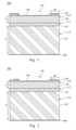
- Fig. 1 is a cross-sectional view of a micro-light-emitting diode (micro-LED) 100 according to the first embodiment not forming part of the present invention.
- micro-LED micro-light-emitting diode
- the micro-LED 100 includes a first type semiconductor layer 110, an active layer 115, a second type semiconductor layer 120, a first dielectric layer 130, and a first electrode 140.
- the second type semiconductor layer 120 is disposed above the first type semiconductor layer 110.
- the active layer 115 is disposed between the first type semiconductor layer 110 and the second type semiconductor layer 120.
- the first dielectric layer 130 is disposed on the second type semiconductor layer 120.
- the first dielectric layer 130 has at least one opening O1 therein to expose at least one part of the second type semiconductor layer 120.
- a first shortest distance D1 between an edge of the opening O1 and a side surface 122 of the second type semiconductor layer 120 is greater than or equal to 1 ⁇ m.
- the first electrode 140 is partially disposed on the first dielectric layer 130 and is electrically coupled with the exposed part of the second type semiconductor layer 120 through the opening O1.
- the opening O1 defines the contact interface between the first electrode 140 and the second type semiconductor layer 120.
- the micro-LED 100 When the micro-LED 100 is forward biased, charge carriers flow from the contact interface between the first electrode 140 and the second type semiconductor layer 120 to the active layer 115. Since the first shortest distance D1 is greater than or equal to 1 ⁇ m, charge carriers spreading to the side surface 122 and/or a side surface 117 of the active area 115 are rare or none. Therefore, the non-radiative recombination occurring at the side surface 117 can be reduced, thereby increasing the efficiency of the micro-LED 100.
- the opening O1 limits the area where the current goes into the micro-LED 100, the current density within the emitting area of the micro-LED 100 increases and can be uniform, thereby increasing the efficiency of the micro-LED 100.
- the leakage currents of the micro-LED 100 can be reduced regardless of the lattice defects in the side surface 122 and/or the side surface 117.
- the opening O1 makes the emitting area of the micro-LED 100 smaller than the size of the micro-LED 100, it is possible to continue miniaturization of the emitting area of the micro-LED 100 while remain the size of the micro-LED 100 to allow the micro-LED 100 to be manufactured with acceptable yield rate.
- a 20 ⁇ m X 20 ⁇ m micro-LED 100 with a 2 ⁇ m X 2 ⁇ m opening can perform the same light output characteristics as a conventional 2 ⁇ m X 2 ⁇ m micro-LED.
- the micro-LED 100 with a larger size has a considerably lower electrostatic sensitivity, a considerably lower surface leakage current, and a considerably lower side surface leakage current due to the lattice defects.
- the size of the micro-LED 100 is smaller than 100 ⁇ m X 100 ⁇ m or 0.01 mm 2 .
- a geometric weighted mean distance between the side surface of the opening O1 and the side surface 122 is greater than or equal to 1 ⁇ m. Furthermore, the area of the opening O1 viewed in a direction normal to the first dielectric layer 130 occupies 2.5%-90% of the total area of the first dielectric layer 130 viewed in the direction normal to the first dielectric layer 130. If the area of the opening O1 occupies less than 2.5% of the total area of the first dielectric layer 130, the opening O1 may be too small, and therefore a complex photolithography process may be needed.
- the first shortest distance D1 may be less than 1 ⁇ m, thereby allowing charge carriers to spread to the side surface 122 and/or the side surface 117.
- the current spreading length of the second type semiconductor layer 120 is less than the current spreading length of the first type semiconductor layer 110. That is, the current spreading length of the first type semiconductor layer 110 is greater than the current spreading length of the second type semiconductor layer 120. In some embodiments, the current spreading length of the first type semiconductor layer 110 is over 20 times greater than the current spreading length of the second type semiconductor layer 120. In this configuration, charge carriers in the second type semiconductor layer 120 are more difficult to spread to the side surface 122 and/or the side surface 117. Therefore, the non-radiative recombination occurring at the side surface 117 can be further reduced, thereby further increasing the efficiency of the micro-LED 100.
- the current spreading length of the semiconductor layer of the diode is proportional to t ⁇ . Therefore, in some embodiments, the first type semiconductor layer 110 has a resistance ⁇ 1 and a thickness t 1 , the second type semiconductor layer 120 has a resistance ⁇ 2 and a thickness t 2 , and t 2 ⁇ 2 ⁇ t 1 ⁇ 1 to make the current spreading length of the second type semiconductor layer 120 to be less than the current spreading length of the first type semiconductor layer 110.
- the first type semiconductor layer 110 is an n type semiconductor layer
- the second type semiconductor layer 120 is a p type semiconductor layer.
- the IV curve for a conventional micro-LED has a steep slope of the forward current versus the forward voltage especially in the mid/low power region near the threshold. This steep slope makes it difficult to control the forward current, and thus the luminance of the conventional micro-LED cannot be easily controlled.
- the first dielectric layer 130 with the opening O1 is disposed on the second type semiconductor layer 120, which has a short current spreading length. Since the second type semiconductor layer 120 has the short current spreading length, the second type semiconductor layer 120 has high resistance and is thin in thickness. In this configuration, the serial resistance of the micro-LED 100 increases, thereby making the slope of the forward current versus the forward voltage gentle. This gentle slope makes it easier to control the forward current, and thus the luminance of the micro-LED 100 can be more easily controlled.
- the first type semiconductor layer 110 is made of, for example, n-doped GaN:Si.
- the thickness of the first type semiconductor layer 110 is in a range from 0.1 ⁇ m to 50 ⁇ m.
- the first type semiconductor layer 110 is formed by, for example, epitaxy.
- the micro-LED 100 of Fig. 1 may further include a second electrode 160.
- the second electrode 160 is at least partially disposed on the first type semiconductor layer 110, such that the first type semiconductor layer 110, the active layer 115, and the second type semiconductor layer 120 are disposed between the first electrode 140 and the second electrode 160.
- the second electrode 160 is electrically coupled with the first type semiconductor layer 110.
- the first electrode 140 is made of a transparent conductive material e.g. indium tin oxide (ITO).
- the second electrode 160 is made of a conductive material, such as metal or a transparent conductive material, e.g. indium tin oxide (ITO).
- the first electrode 140 and the second electrode 160 can be formed by, for example, physical vapor deposition (PVD) or chemical vapor deposition (CVD).
- the first type semiconductor layer 110 may include an optional ohmic contact layer to reduce the contact resistance between the second electrode 160 and the first type semiconductor layer 110.
- the ohmic contact layer and the rest of the first type semiconductor layer 110 are made of, for example, n-doped GaN:Si, while the ohm contact layer is doped more heavily than the rest of the first type semiconductor layer 110.
- the thickness of the ohmic contact layer is in a range from 5 nm to 2 ⁇ m.
- the thickness of the rest of the first type semiconductor layer 110 is in a range from 0.1 ⁇ m to 50 ⁇ m.
- the second type semiconductor layer 120 is made of, for example, p-doped GaN or p-doped AlGaInP.
- the thickness of the second type semiconductor layer 120 is in a range from 50 nm to 20 ⁇ m.
- the second type semiconductor layer 120 is formed by, for example, epitaxy.
- the second type semiconductor layer 120 may include an optional ohmic contact layer to reduce the contact resistance between the first electrode 140 and the second type semiconductor layer 120.
- the ohmic contact layer and the rest of the second type semiconductor layer 120 are made of, for example, p-doped GaN or p-doped AlGaInP, while the ohm contact layer is doped more heavily than the rest of the second type semiconductor layer 120.
- the ohmic contact layer is made of, for example, InGaN
- the rest of the second type semiconductor layer 120 is made of, for example, p-doped GaN or p-doped AlGaInP.
- the thickness of the ohmic contact layer is in a range from 5 nm to 2 ⁇ m.
- the thickness of the rest of the second type semiconductor layer 120 is in a range from 50 nm to 20 ⁇ m.
- the active layer 115 is made of, for example, heterostructure or quantum well structure.
- the thickness of the active layer 115 is in a range from 50 nm to 5 ⁇ m.
- the active layer 115 is formed by, for example, epitaxy.
- the active layer 115 can be omitted. In the case that the active layer 115 is omitted, the second type semiconductor layer 120 is disposed on the first type semiconductor layer 110.
- the first dielectric layer 130 is made of a dielectric material, such as silicon nitride or silicon dioxide.
- the thickness of the first dielectric layer 130 is in a range from 10 nm to 5 ⁇ m.
- the first dielectric layer 130 is formed by, for example, physical vapor deposition (PVD).
- a combination of the first type semiconductor layer 110, the active layer 115, the second type semiconductor layer 120, and the first dielectric layer 130 with the opening O1 is a solid with at least two planes.
- the combination of the first type semiconductor layer 110, the active layer 115, the second type semiconductor layer 120, and the first dielectric layer 130 with the opening O1 is a cylinder, a polyhedron, or a trapezoidal solid.
- Fig. 2 is a cross-sectional view of a micro-LED 100 according to the second embodiment not forming part of the present invention.
- the difference between this embodiment and the first embodiment is that the first electrode 140 of Fig. 2 partially covers the upper surface of the first dielectric layer 130, while the first electrode 140 of Fig. 1 fully covers the upper surface of the first dielectric layer 130.
- micro-LED 100 of Fig. 2 are similar to the micro-LED 100 of Fig. 1 and therefore are not repeated here to avoid duplicity.
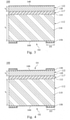
- Fig. 3 is a cross-sectional view of a micro-LED 100 according to an embodiment not forming part of this invention.
- the micro-LED 100 further includes a second dielectric layer 150, while the first dielectric layer 130 is omitted.
- the second dielectric layer 150 is disposed on the first type semiconductor layer 110.
- the second dielectric layer 150 has at least one opening 02 therein to expose at least one part of the first type semiconductor layer 110.
- a second shortest distance D2 between an edge of the opening 02 and a side surface 112 of the first type semiconductor layer 110 is greater than or equal to 1 ⁇ m.
- the second electrode 160 is partially disposed on the second dielectric layer 150 and is electrically coupled with the exposed part of the first type semiconductor layer 110 through the opening 02.
- the opening 02 due to the opening 02, charge carriers spreading to the side surface 112 and/or the side surface 117 are rare or none, thereby reducing the non-radiative recombination occurring at the side surface 117.
- the first dielectric layer 130 with the opening O1 can be replaced by the second dielectric layer 150 with the opening 02 to reduce the non-radiative recombination occurring at the side surface 117.
- Other details regarding the second dielectric layer 150 with the opening 02 are similar to the first dielectric layer 130 with the opening O1.
- micro-LED 100 of Fig. 3 are similar to the micro-LED 100 of Fig. 1 and therefore are not repeated here to avoid duplicity.
- Fig. 4 is a cross-sectional view of a micro-LED 100 according to the forth embodiment forming part of the present invention.
- the difference between this embodiment and the first or third embodiment is that the micro-LED 100 of Fig. 4 includes both the first dielectric layer 130 with the opening O1 and the second dielectric layer 150 with the opening 02.
- micro-LED 100 of Fig. 4 are similar to the micro-LEDs 100 of Figs. 1 and 3 and therefore are not repeated here to avoid duplicity.
- Fig. 5 is a cross-sectional view of a micro-LED 100 according to the fifth embodiment not forming part of the present invention. Similar to the first dielectric layer 130 of Fig. 1 , the first dielectric layer 130 of Fig. 5 partially cover a major surface of the second type semiconductor layer 120 distal to the first type semiconductor layer 110. The difference between the first dielectric layer 130 of Fig. 5 and the first dielectric layer 130 of Fig. 1 is that the first dielectric layer 130 of Fig. 5 further at least partially covers the side surface 122. In this configuration, the side surface 122 can be protected from moisture and mechanical damage by the first dielectric layer 130.
- micro-LED 100 of Fig. 5 are similar to the micro-LED 100 of Fig. 1 and therefore are not repeated here to avoid duplicity.
- Fig. 6 is a cross-sectional view of a micro-LED 100 according to the sixth embodiment not forming part of the present invention.
- the difference between the first dielectric layer 130 of Fig. 6 and the first dielectric layer 130 of Fig. 5 is that the first dielectric layer 130 of Fig. 6 further at least partially covers the side surface 117 and/or the side surface 112. In this configuration, the side surface 117 and/or the side surface 112 can be protected from moisture and mechanical damage by the first dielectric layer 130.
- micro-LED 100 of Fig. 6 are similar to the micro-LED 100 of Fig. 5 and therefore are not repeated here to avoid duplicity.
- Fig. 7 is a cross-sectional view of a micro-LED 100 according to the seventh embodiment forming part of the present invention.
- the difference between the first and second dielectric layers 130/150 of Fig. 7 and the first and second dielectric layers 130/150 of Fig. 4 is that the first and second dielectric layers 130/150 of Fig. 7 further at least partially covers the side surface 122, the side surface 117, and/or the side surface 112.
- the side surface 122, the side surface 117, and/or the side surface 112 can be protected from moisture and mechanical damage by the first and second dielectric layers 130/150.
- micro-LED 100 of Fig. 7 are similar to the micro-LED 100 of Fig. 4 and therefore are not repeated here to avoid duplicity.
- Fig. 8 is a plan view of a micro-LED 100 according to the eighth embodiment of this invention, wherein the first or second electrode 140 or 160 is removed.
- the first or second dielectric layer 130 or 150 has a plurality of the openings O1 or 02 therein.
- the number of the openings O1 or 02 is in a range from 1 to 1000.
- the openings O1 or 02 are arranged in an array, and the openings O1 or 02 have the same shape. More specifically, the openings O1 or 02 of Fig. 8 are circular in shape.
- micro-LED 100 of Fig. 8 are similar to the micro-LED 100 of Fig. 1 and therefore are not repeated here to avoid duplicity.
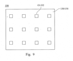
- Fig. 9 is a plan view of a micro-LED 100 according to the ninth embodiment of this invention, wherein the first or second electrode 140 or 160 is removed.
- the difference between the micro-LED 100 of Fig. 9 and the micro-LED 100 of Fig. 8 is that the openings O1 or O2 of Fig. 9 are rectangular in shape.
- micro-LED 100 of Fig. 9 Other details regarding the micro-LED 100 of Fig. 9 are similar to the micro-LED 100 of Fig. 9 and therefore are not repeated here to avoid duplicity.
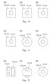
- Fig. 10 is a plan view of a plurality of micro-LEDs 100 according to the tenth embodiment of this invention, wherein the first or second electrodes 140 or 160 are removed. As shown in Fig. 10 , the micro-LEDs 100 are arranged in an array. The micro-LEDs 100 have the same shape, while the openings O1 or 02 have different shapes.
- micro-LEDs 100 of Fig. 10 are similar to the micro-LED 100 of Fig. 1 and therefore are not repeated here to avoid duplicity.
- Fig. 11 is a plan view of a plurality of micro-LEDs 100 according to the eleventh embodiment of this invention, wherein the first or second electrodes 140 or 160 are removed. As shown in Fig. 11 , the micro-LEDs 100 are arranged in an array. The micro-LEDs 100 have different shapes, while the openings O1 or 02 have the same shape.
- micro-LEDs 100 of Fig. 11 are similar to the micro-LEDs 100 of Fig. 10 and therefore are not repeated here to avoid duplicity.
- Fig. 12 is a plan view of a plurality of micro-LEDs 100 according to the twelfth embodiment of this invention, wherein the first or second electrodes 140 or 160 are removed.
- the micro-LEDs 100 are arranged in an array.
- the micro-LEDs 100 have different shapes, and the openings O1 or O2 have different shapes as well. That is, the openings O1 or O2 for any one of the micro-LEDs 100 are different from the openings O1 or O2 for any other of the micro-LEDs 100.
- the openings O1 or O2 for each micro-LED 100 also have different shapes, i.e. are different from each other.
- the number of the openings O1 or O2 for each micro-LED 100 is one, two, or three, and the openings O1 or O2 can be circular or polygonal in shape.
- micro-LEDs 100 of Fig. 12 are similar to the micro-LEDs 100 of Fig. 11 and therefore are not repeated here to avoid duplicity.
Landscapes
- Engineering & Computer Science (AREA)
- Manufacturing & Machinery (AREA)
- Computer Hardware Design (AREA)
- Microelectronics & Electronic Packaging (AREA)
- Power Engineering (AREA)
- Led Devices (AREA)
Description
- This application claims priority to
United States Application Serial Number 14/290,999, filed May 30th, 2014 - The present disclosure relates to micro-light-emitting diodes (micro-LEDs).
- In the recent years, light-emitting diodes (LEDs) have become popular in general and commercial lighting applications. As light sources, LEDs have many advantages including lower energy consumption, longer lifetime, smaller size, and faster switching, and hence conventional lighting, such as incandescent lighting, is gradually replaced by LED
lights. - In an LED, when electrons and holes recombine across the semiconductor gap, the recombination energy is emitted in the form of photons and generates light. This recombination mechanism is the so-called radiative recombination. However, when electrons and holes recombine through intermediate electronic states in the semiconductor gap, then the recombination energy is emitted in the form of heat instead of photons, reducing the light emission efficiency of the LED. This recombination mechanism is the so-called non-radiative recombination. On the side surface of an LED, typically there are a large number of surface and defect states. Therefore, a fraction of electrons and holes that are close to the side surface of the LED will non-radiatively recombine through these surface and defect states. This non-radiative recombination generates heat instead of light, considerably reducing the efficiency of the LED. This problem becomes more and more serious as miniaturization of LEDs proceeds to microscale since electrons and holes can spread to the side surface easily in a micro-LED.
- Furthermore, since electrons and holes can spread to the side surface easily in a micro-LED, the current density may be too low and uneven within the emitting area of the micro-LED. The low and uneven current density within the emitting area of the micro-LED reduces the efficiency of the micro-LED as well.
- Moreover, typically there are a large number of lattice defects in the side surface of an LED due to the etching and/or scribing process. These lattice defects result in leakage currents. As miniaturization of LEDs proceeds to microscale, the ratio of the lattice defects to the lattice sites of a micro-LED increases, thereby raising the ratio of the leakage currents to the total currents of the micro-LED and reducing the efficiency of the micro-LED.
- Furthermore, as miniaturization of LEDs proceeds to microscale, the process variation tolerance of micro-LEDs decreases, and therefore the yield rate of micro-LEDs decreases. In addition, transferring, controlling, operating, and handling of micro-LEDs also become more and more difficult.
- The document
JPS63194375 A - According to one embodiment of this invention, a micro-light-emitting diode (micro-LED) includes a micro-light-emitting diode as recited in claim 1.
- The opening defines the contact interface between the first electrode and the second type semiconductor layer. When the micro-LED is forward biased, charge carriers flow from the contact interface between the first electrode and the second type semiconductor layer to the junction of the first type semiconductor layer and the second type semiconductor layer. Since the first shortest distance is greater than or equal to 1 µm, charge carriers spreading to the side surface of the micro-LED are rare or none. Therefore, the non-radiative recombination occurring at the side surface of the micro-LED can be reduced, thereby increasing the efficiency of the micro-LED.
- Furthermore, since the opening limits the area where the current goes into the micro-LED, the current density within the emitting area of the micro-LED increases and can be more uniform, thereby increasing the efficiency of the micro-LED.
- Moreover, since charge carriers spreading to the side surface of the micro-LED are rare or none, the leakage currents of the micro-LED can be reduced regardless of the lattice defects in the side surface of the micro-LED.
- Furthermore, since the opening makes the emitting area of the micro-LED smaller than the size of the micro-LED, it is possible to continue miniaturization of the emitting area of the micro-LED while remain the size of the micro-LED to allow the micro-LED to be manufactured with acceptable yield rate. In addition, the micro-LED with a larger size has a considerably lower electrostatic sensitivity, a considerably lower surface leakage current, and a considerably lower side surface leakage current due to the lattice defects.
-
-
Fig. 1 is a cross-sectional view of a micro-light-emitting diode (micro-LED) according to the first embodiment not forming part of the present invention; -
Fig. 2 is a cross-sectional view of a micro-LED according to the second embodiment not forming part of the present invention; -
Fig. 3 is a cross-sectional view of a micro-LED according to a third embodiment not forming part of the present invention; -
Fig. 4 is a cross-sectional view of a micro-LED according the fourth embodiment forming part of the present invention; -
Fig. 5 is a cross-sectional view of a micro-LED according to the fifth embodiment not forming part of the present invention; -
Fig. 6 is a cross-sectional view of a micro-LED according to the sixth embodiment not forming part of the present invention; -
Fig. 7 is a cross-sectional view of a micro-LED according to the seventh embodiment forming part of the present invention; -
Fig. 8 is a plan view of a micro-LED according to the eighth embodiment of this invention, wherein the first or second electrode is removed; -
Fig. 9 is a plan view of a micro-LED according to the ninth embodiment of this invention, wherein the first or second electrode is removed; -
Fig. 10 is a plan view of a plurality of micro-LEDs according to the tenth embodiment of this invention, wherein the first or second electrodes are removed; -
Fig. 11 is a plan view of a plurality of micro-LEDs according to the eleventh embodiment of this invention, wherein the first or second electrodes are removed; and -
Fig. 12 is a plan view of a plurality of micro-LEDs according to the twelfth embodiment of this invention, wherein the first or second electrodes are removed. - In the following detailed description, for purposes of explanation, numerous specific details are set forth in order to provide a thorough understanding of the disclosed embodiments. It will be apparent, however, that one or more embodiments may be practiced without these specific details. In other instances, well-known structures and devices are schematically shown in order to simplify the drawing.
-
Fig. 1 is a cross-sectional view of a micro-light-emitting diode (micro-LED) 100 according to the first embodiment not forming part of the present invention. - The micro-LED 100 includes a first
type semiconductor layer 110, anactive layer 115, a secondtype semiconductor layer 120, a firstdielectric layer 130, and afirst electrode 140. The secondtype semiconductor layer 120 is disposed above the firsttype semiconductor layer 110. Theactive layer 115 is disposed between the firsttype semiconductor layer 110 and the secondtype semiconductor layer 120. The firstdielectric layer 130 is disposed on the secondtype semiconductor layer 120. The firstdielectric layer 130 has at least one opening O1 therein to expose at least one part of the secondtype semiconductor layer 120. A first shortest distance D1 between an edge of the opening O1 and aside surface 122 of the secondtype semiconductor layer 120 is greater than or equal to 1 µm. The first
electrode 140 is partially disposed on the firstdielectric layer 130 and is electrically coupled with the exposed part of the secondtype semiconductor layer 120 through the opening O1. - As shown in
Fig. 1 , the opening O1 defines the contact interface between thefirst electrode 140 and the secondtype semiconductor layer 120. When the micro-LED 100 is forward biased, charge carriers flow from the contact interface between thefirst electrode 140 and the secondtype semiconductor layer 120 to theactive layer 115. Since the first shortest distance D1 is greater than or equal to 1 µm, charge carriers spreading to theside surface 122 and/or aside surface 117 of theactive area 115 are rare or none. Therefore, the non-radiative recombination occurring at theside surface 117 can be reduced, thereby increasing the efficiency of the micro-LED 100. - Furthermore, since the opening O1 limits the area where the current goes into the micro-LED 100, the current density within the emitting area of the micro-LED 100 increases and can be uniform, thereby increasing the efficiency of the
micro-LED 100. - Moreover, since charge carriers spreading to the
side surface 122 and/or theside surface 117 are rare or none, the leakage currents of the micro-LED 100 can be reduced regardless of the lattice defects in theside surface 122 and/or theside surface 117. - Furthermore, since the opening O1 makes the emitting area of the micro-LED 100 smaller than the size of the micro-LED 100, it is possible to continue miniaturization of the emitting area of the micro-LED 100 while remain the size of the micro-LED 100 to allow the micro-LED 100 to be manufactured with acceptable yield rate. For example, a 20 µm X 20
µ m micro-LED 100 with a 2 µm X 2 µm opening can perform the same light output characteristics as a conventional 2 µm X 2 µm micro-LED. In addition, the micro-LED 100 with a larger size has a considerably lower electrostatic sensitivity, a considerably lower surface leakage current, and a considerably lower side surface leakage current due to the lattice defects. - In the embodiment of the present invention, the size of the
micro-LED 100 is smaller than 100µm X 100
µm or 0.01 mm2. - In some embodiments, a geometric weighted mean distance between the side surface of the opening O1 and the
side surface 122 is greater than or equal to 1 µm.
Furthermore, the area of the opening O1 viewed in a direction normal to thefirst dielectric layer 130 occupies 2.5%-90% of the total area of thefirst dielectric layer 130 viewed in the direction normal to thefirst dielectric layer 130. If the area of the opening O1 occupies less than 2.5% of the total area of thefirst dielectric layer 130, the opening O1 may be too small, and therefore a complex photolithography process may be needed. If the area of the opening O1 occupies greater than 90% of the total area of thefirst dielectric layer 130, the first shortest distance D1 may be less than 1 µm, thereby allowing charge carriers to spread to theside surface 122 and/or theside surface 117. - In some embodiments, the current spreading length of the second
type semiconductor layer 120 is less than the current spreading length of the firsttype semiconductor layer 110. That is, the current spreading length of the firsttype semiconductor layer 110 is greater than the current spreading length of the secondtype semiconductor layer 120. In some embodiments, the current spreading length of the firsttype semiconductor layer 110 is over 20 times greater than the current spreading length of the secondtype semiconductor layer 120. In this configuration, charge carriers in the secondtype semiconductor layer 120 are more difficult to spread to theside surface 122 and/or theside surface 117. Therefore, the non-radiative recombination occurring at theside surface 117 can be further reduced, thereby further increasing the efficiency of themicro-LED 100. - The current spreading length of a semiconductor layer of a diode is determined by the following equation I:

- As confirmed by the aforementioned equation I, the current spreading length of the semiconductor layer of the diode is proportional to

type semiconductor layer 110 has a resistance ρ 1 and a thickness t1, the secondtype semiconductor layer 120 has a resistance ρ 2 and a thickness t2, and
type semiconductor layer 120 to be less than the current spreading length of the firsttype semiconductor layer 110. - In some embodiments, the first
type semiconductor layer 110 is an n type semiconductor layer, and the secondtype semiconductor layer 120 is a p type semiconductor layer. - In addition, the IV curve for a conventional micro-LED has a steep slope of the forward current versus the forward voltage especially in the mid/low power region near the threshold. This steep slope makes it difficult to control the forward current, and thus the luminance of the conventional micro-LED cannot be easily controlled.
- Therefore, in some embodiments, the
first dielectric layer 130 with the opening O1 is disposed on the secondtype semiconductor layer 120, which has a short current spreading length. Since the secondtype semiconductor layer 120 has the short current spreading length, the secondtype semiconductor layer 120 has high resistance and is thin in thickness. In this configuration, the serial resistance of the micro-LED 100 increases, thereby making the slope of the forward current versus the forward voltage gentle. This gentle slope makes it easier to control the forward current, and thus the luminance of the micro-LED 100 can be more easily controlled. - In some embodiments, the first
type semiconductor layer 110 is made of, for example, n-doped GaN:Si. The thickness of the firsttype semiconductor layer 110 is in a range from 0.1 µm to 50 µm. The firsttype semiconductor layer 110 is formed by, for example, epitaxy. - The
micro-LED 100 ofFig. 1 may further include asecond electrode 160. Thesecond electrode 160 is at least partially disposed on the firsttype semiconductor layer 110, such that the firsttype semiconductor layer 110, theactive layer 115, and the secondtype semiconductor layer 120 are disposed between thefirst electrode 140 and thesecond electrode 160. Thesecond electrode 160 is electrically coupled with the firsttype semiconductor layer 110. Thefirst electrode 140 is made of a transparent conductive material e.g. indium tin oxide (ITO). Thesecond electrode 160 is made of a conductive material, such as metal or a transparent conductive material, e.g. indium tin oxide (ITO). Thefirst electrode 140 and thesecond electrode 160 can be formed by, for example, physical vapor deposition (PVD) or chemical vapor deposition (CVD). - In some embodiments, the first
type semiconductor layer 110 may include an optional ohmic contact layer to reduce the contact resistance between the second electrode
160 and the firsttype semiconductor layer 110. In some embodiments, the ohmic contact
layer and the rest of the firsttype semiconductor layer 110 are made of, for example, n-doped GaN:Si, while the ohm contact layer is doped more heavily than the rest of the firsttype semiconductor layer 110. The thickness of the ohmic contact layer is in a range
from 5 nm to 2 µm. The thickness of the rest of the firsttype semiconductor layer 110 is in a range from 0.1 µm to 50 µm. - In some embodiments, the second
type semiconductor layer 120 is made of, for example, p-doped GaN or p-doped AlGaInP. The thickness of the secondtype semiconductor layer 120 is in a range from 50 nm to 20 µm. The secondtype semiconductor layer 120 is formed by, for example, epitaxy. - Similarly, the second
type semiconductor layer 120 may include an optional ohmic
contact layer to reduce the contact resistance between thefirst electrode 140 and the secondtype semiconductor layer 120. In some embodiments, the ohmic contact layer and
the rest of the secondtype semiconductor layer 120 are made of, for example, p-doped GaN or p-doped AlGaInP, while the ohm contact layer is doped more heavily than the rest of the secondtype semiconductor layer 120. Alternatively, the ohmic contact layer is made
of, for example, InGaN, and the rest of the secondtype semiconductor layer 120 is made of, for example, p-doped GaN or p-doped AlGaInP. The thickness of the ohmic contact
layer is in a range from 5 nm to 2 µm. The thickness of the rest of the secondtype semiconductor layer 120 is in a range from 50 nm to 20 µm. - In some embodiments, the
active layer 115 is made of, for example, heterostructure or quantum well structure. The thickness of theactive layer 115 is in a range from 50 nm to 5 µm. Theactive layer 115 is formed by, for example, epitaxy. - In some embodiments, the
active layer 115 can be omitted. In the case that theactive layer 115 is omitted, the secondtype semiconductor layer 120 is disposed on the firsttype semiconductor layer 110. - In some embodiments, the
first dielectric layer 130 is made of a dielectric material, such as silicon nitride or silicon dioxide. The thickness of thefirst dielectric layer 130 is in a range from 10 nm to 5 µm. Thefirst dielectric layer 130 is formed by, for example, physical vapor deposition (PVD). - In some embodiments, a combination of the first
type semiconductor layer 110, theactive layer 115, the secondtype semiconductor layer 120, and thefirst dielectric layer 130 with the opening O1 is a solid with at least two planes. For example, the combination of the firsttype semiconductor layer 110, theactive layer 115, the secondtype semiconductor layer 120, and thefirst dielectric layer 130 with the opening O1 is a cylinder, a polyhedron, or a trapezoidal solid. -
Fig. 2 is a cross-sectional view of a micro-LED 100 according to the second embodiment not forming part of the present invention. The difference between this embodiment and the first
embodiment is that thefirst electrode 140 ofFig. 2 partially covers the upper surface of thefirst dielectric layer 130, while thefirst electrode 140 ofFig. 1 fully covers the upper surface of thefirst dielectric layer 130. - Other details regarding the
micro-LED 100 ofFig. 2 are similar to themicro-LED 100 ofFig. 1 and therefore are not repeated here to avoid duplicity. -
Fig. 3 is a cross-sectional view of a micro-LED 100 according to an embodiment not forming part
of this invention. The difference between this embodiment and the first
embodiment is that the micro-LED 100 further includes asecond dielectric layer 150, while thefirst dielectric layer 130 is omitted. Thesecond dielectric layer 150 is disposed on the firsttype semiconductor layer 110. Thesecond dielectric layer 150 has at least oneopening 02 therein to expose at least one part of the firsttype semiconductor layer 110. A second shortest distance D2 between an edge of theopening 02 and aside surface 112 of the firsttype semiconductor layer 110 is greater than or equal to 1 µm. Thesecond electrode 160 is partially disposed on thesecond dielectric layer 150 and is electrically coupled with the exposed part of the firsttype semiconductor layer 110 through theopening 02. - Similarly, due to the
opening 02, charge carriers spreading to theside surface 112 and/or theside surface 117 are rare or none, thereby reducing the non-radiative recombination occurring at theside surface 117. In the case that the current spreading length of the firsttype semiconductor layer 110 is not over 20 times greater than the current spreading length of the secondtype semiconductor layer 120, thefirst dielectric layer 130 with the opening O1 can be replaced by thesecond dielectric layer 150 with theopening 02 to reduce the non-radiative recombination occurring at theside surface 117. Other details regarding thesecond dielectric layer 150 with theopening 02 are similar to thefirst dielectric layer 130 with the opening O1. - Other details regarding the
micro-LED 100 ofFig. 3 are similar to themicro-LED 100 ofFig. 1 and therefore are not repeated here to avoid duplicity. -
Fig. 4 is a cross-sectional view of a micro-LED 100 according to the forth embodiment forming part of the present invention. The difference between this embodiment and the first or
third embodiment is that themicro-LED 100 ofFig. 4 includes both thefirst dielectric layer 130 with the opening O1 and thesecond dielectric layer 150 with theopening 02. - Other details regarding the
micro-LED 100 ofFig. 4 are similar to themicro-LEDs 100 ofFigs. 1 and3 and therefore are not repeated here to avoid duplicity. -
Fig. 5 is a cross-sectional view of a micro-LED 100 according to the fifth embodiment not forming part of the present invention. Similar to thefirst dielectric layer 130 ofFig. 1 , thefirst dielectric layer 130 ofFig. 5 partially cover a major surface of the secondtype semiconductor layer 120 distal to the firsttype semiconductor layer 110. The difference between thefirst dielectric layer 130 ofFig. 5 and thefirst dielectric layer 130 ofFig. 1 is that thefirst dielectric layer 130 ofFig. 5 further at least partially covers theside surface 122. In this configuration, theside surface 122 can be protected from moisture and mechanical damage by thefirst dielectric layer 130. - Other details regarding the
micro-LED 100 ofFig. 5 are similar to themicro-LED 100 ofFig. 1 and therefore are not repeated here to avoid duplicity. -
Fig. 6 is a cross-sectional view of a micro-LED 100 according to the sixth embodiment not forming part of the present invention. The difference between thefirst dielectric layer 130 of Fig.
6 and thefirst dielectric layer 130 ofFig. 5 is that thefirst dielectric layer 130 ofFig. 6 further at least partially covers theside surface 117 and/or theside surface 112. In this configuration, theside surface 117 and/or theside surface 112 can be protected from moisture and mechanical damage by thefirst dielectric layer 130. - Other details regarding the
micro-LED 100 ofFig. 6 are similar to themicro-LED 100 ofFig. 5 and therefore are not repeated here to avoid duplicity. -
Fig. 7 is a cross-sectional view of a micro-LED 100 according to the seventh embodiment forming part of the present invention. The difference between the first and second dielectric
layers 130/150 ofFig. 7 and the first and seconddielectric layers 130/150 ofFig. 4 is that the first and seconddielectric layers 130/150 ofFig. 7 further at least partially covers theside surface 122, theside surface 117, and/or theside surface 112. In this configuration, theside surface 122, theside surface 117, and/or theside surface 112 can be protected from moisture and mechanical damage by the first and seconddielectric layers 130/150. - Other details regarding the
micro-LED 100 ofFig. 7 are similar to themicro-LED 100 ofFig. 4 and therefore are not repeated here to avoid duplicity. -
Fig. 8 is a plan view of a micro-LED 100 according to the eighth embodiment of this invention, wherein the first orsecond electrode Fig. 8 , the first or seconddielectric layer Fig. 8 are circular in shape. - Other details regarding the
micro-LED 100 ofFig. 8 are similar to themicro-LED 100 ofFig. 1 and therefore are not repeated here to avoid duplicity. -
Fig. 9 is a plan view of a micro-LED 100 according to the ninth embodiment of this invention, wherein the first orsecond electrode micro-LED 100 ofFig. 9 and themicro-LED 100 ofFig. 8 is that the openings O1 or O2 ofFig. 9 are rectangular in shape. - Other details regarding the
micro-LED 100 ofFig. 9 are similar to themicro-LED 100 ofFig. 9 and therefore are not repeated here to avoid duplicity. -
Fig. 10 is a plan view of a plurality ofmicro-LEDs 100 according to the tenth embodiment of this invention, wherein the first orsecond electrodes Fig. 10 , the micro-LEDs 100 are arranged in an array. The micro-LEDs 100 have the same shape, while the openings O1 or 02 have different shapes. - Other details regarding the
micro-LEDs 100 ofFig. 10 are similar to themicro-LED 100 ofFig. 1 and therefore are not repeated here to avoid duplicity. -
Fig. 11 is a plan view of a plurality ofmicro-LEDs 100 according to the eleventh embodiment of this invention, wherein the first orsecond electrodes Fig. 11 , the micro-LEDs 100 are arranged in an array. The micro-LEDs 100 have different shapes, while the openings O1 or 02 have the same shape. - Other details regarding the
micro-LEDs 100 ofFig. 11 are similar to themicro-LEDs 100 ofFig. 10 and therefore are not repeated here to avoid duplicity. -
Fig. 12 is a plan view of a plurality ofmicro-LEDs 100 according to the twelfth embodiment of this invention, wherein the first orsecond electrodes Fig. 12 , the micro-LEDs 100 are arranged in an array. The micro-LEDs 100 have different shapes, and the openings O1 or O2 have different shapes as well. That is, the openings O1 or O2 for any one of the micro-LEDs 100 are different from the openings O1 or O2 for any other of the micro-LEDs 100. Furthermore, the openings O1 or O2 for each micro-LED 100 also have different shapes, i.e. are different from each other. As shown inFig. 12 , the number of the openings O1 or O2 for each micro-LED 100 is one, two, or three, and the openings O1 or O2 can be circular or polygonal in shape. - Other details regarding the
micro-LEDs 100 ofFig. 12 are similar to themicro-LEDs 100 ofFig. 11 and therefore are not repeated here to avoid duplicity.
Claims (19)
- A micro-light-emitting diode (micro-LED, 100) with a size thereof smaller than 100 µm X 100 µm or 0.01 mm2, comprising:a first type semiconductor layer (110);a second type semiconductor layer (120) disposed on or above the first type semiconductor layer (110);a first dielectric layer (130) disposed on the second type semiconductor layer (120), the first dielectric layer (130) having at least one opening (O1) therein to expose at least one part of the second type semiconductor layer, (120) wherein a first shortest distance (D1) between an edge of the opening (O1) of the first dielectric layer (130) and a side surface (122) of the second type semiconductor layer (120) is greater than or equal to 1 µm;a first electrode (140) partially disposed on the first dielectric layer (130) and electrically coupled with the exposed part of the second type semiconductor layer (120) through the opening (O1) of the first dielectric layer (130), characterized in that the first electrode (140) is made of a transparent conductive material;a second dielectric layer (150) disposed on the first type semiconductor layer (110), the second dielectric layer (150) having at least one opening (02) therein to expose at least one part of the first type semiconductor layer (110), wherein a second shortest distance (D2) between an edge of the opening (02) of the second dielectric layer (150) and a side surface of the first type semiconductor layer (110) is greater than or equal to 1 µm; anda second electrode (160) partially disposed on the second dielectric layer (150) and electrically coupled with the exposed part of the first type semiconductor layer (110) through the opening (02) of the second dielectric layer (150).
- The micro-LED (100) of claim 1, wherein a geometric weighted mean distance between the side surface of the opening (O1) of the first dielectric layer (130) and the side surface (122) of the second type semiconductor layer (120) is greater than or equal to 1 µm.
- The micro-LED (100) of claim 1, wherein the first type semiconductor layer (110) has a resistance ρ 1 and a thickness t1, the second type semiconductor layer (120) has a resistance ρ 2 and a thickness t2, and

- The micro-LED (100) of claim 1, wherein the first type semiconductor layer (110) is an n type semiconductor layer, and the second type semiconductor layer (120) is a p type semiconductor layer.
- The micro-LED (100) of claim 1, wherein the current spreading length of the first type semiconductor layer (110) is over 20 times greater than the current spreading length of the second type semiconductor layer (120).
- The micro-LED (100) of claim 1, wherein the first type semiconductor layer (110) has a resistance ρ 1 and a thickness t1, the second type semiconductor layer (120) has a resistance ρ 2 and a thickness t2, and

- The micro-LED (100) of claim 1, wherein the first type semiconductor layer (110) is a p type semiconductor layer, and the second type semiconductor layer (120) is an n type semiconductor layer.
- The micro-LED (100) of claim 1, wherein the number of the opening of the first dielectric layer (110) is in a range from 1 to 1000.
- The micro-LED (100) of claim 1, wherein the area of the opening of the first dielectric layer viewed in a direction normal to the first dielectric layer occupies 2.5%-90% of the total area of the first dielectric layer viewed in the direction normal to the first dielectric layer.
- The micro-LED (100) of claim 1, wherein the first dielectric layer (130) partially covers a major surface of the second type semiconductor layer (120) distal to the first type semiconductor layer (110).
- The micro-LED (100) of claim 10, wherein the first dielectric layer (130) at least partially covers the side surface (122) of the second type semiconductor layer (120).
- The micro-LED (100) of claim 11, further comprising:
an active layer (115) disposed between the first type semiconductor layer (110) and the second type semiconductor layer (120), wherein the first dielectric layer (130) at least partially covers a side surface (117) of the active layer (115). - The micro-LED (100) of claim 12, wherein the first dielectric layer (130) at least partially covers a side surface (112) of the first type semiconductor layer (110).
- The micro-LED (100) of claim 1, further comprising:
a second electrode (160) at least partially disposed on the first type semiconductor layer (110), such that at least the first type semiconductor layer (110) and the second type semiconductor layer (120) are disposed between the first electrode (140) and the second electrode (160). - The micro-LED (100) of claim 1, further comprising:
an active layer (115) disposed between the first type semiconductor layer (110) and the second type semiconductor layer (120), wherein a combination of the first type semiconductor layer (110), the active layer (115), the second type semiconductor layer (120), and the first dielectric layer (130) with the opening (O1) is a solid with at least two planes. - The micro-LED (100) of claim 15, wherein the combination of the first type semiconductor layer (110), the active layer (115), the second type semiconductor layer (120), and the first dielectric layer (130) with the opening (O1) is a cylinder, a polyhedron, or a trapezoidal solid.
- The micro-LED (100) of claim 1, wherein the number of the opening (O1) of the first dielectric layer (130) is one, two, or three.
- The micro-LED (100) of claim 1, wherein a plurality of the openings (O1) of the first dielectric layer (130) have the same shape.
- The micro-LED (100) of claim 1, wherein a plurality of the openings (O1) of the first dielectric layer (130) have different shapes.
Applications Claiming Priority (2)
| Application Number | Priority Date | Filing Date | Title |
|---|---|---|---|
| US14/290,999 US9105813B1 (en) | 2014-05-30 | 2014-05-30 | Micro-light-emitting diode |
| PCT/CN2015/079957 WO2015180651A1 (en) | 2014-05-30 | 2015-05-27 | Micro-light-emitting diode |
Publications (3)
| Publication Number | Publication Date |
|---|---|
| EP3149780A1 EP3149780A1 (en) | 2017-04-05 |
| EP3149780A4 EP3149780A4 (en) | 2017-10-25 |
| EP3149780B1 true EP3149780B1 (en) | 2022-03-16 |
Family
ID=53763334
Family Applications (1)
| Application Number | Title | Priority Date | Filing Date |
|---|---|---|---|
| EP15798982.3A Active EP3149780B1 (en) | 2014-05-30 | 2015-05-27 | Micro-light-emitting diode |
Country Status (5)
| Country | Link |
|---|---|
| US (1) | US9105813B1 (en) |
| EP (1) | EP3149780B1 (en) |
| JP (1) | JP6162890B2 (en) |
| CN (1) | CN105355733B (en) |
| WO (1) | WO2015180651A1 (en) |
Families Citing this family (43)
| Publication number | Priority date | Publication date | Assignee | Title |
|---|---|---|---|---|
| US9899329B2 (en) | 2010-11-23 | 2018-02-20 | X-Celeprint Limited | Interconnection structures and methods for transfer-printed integrated circuit elements with improved interconnection alignment tolerance |
| US8934259B2 (en) | 2011-06-08 | 2015-01-13 | Semprius, Inc. | Substrates with transferable chiplets |
| US10158043B2 (en) * | 2014-05-30 | 2018-12-18 | Mikro Mesa Technolgy Co., Ltd. | Light-emitting diode and method for manufacturing the same |
| CN110010750B (en) | 2014-06-18 | 2021-11-09 | 艾克斯展示公司技术有限公司 | Micro-assembly LED display |
| US9716082B2 (en) | 2014-08-26 | 2017-07-25 | X-Celeprint Limited | Micro assembled hybrid displays and lighting elements |
| US9818725B2 (en) | 2015-06-01 | 2017-11-14 | X-Celeprint Limited | Inorganic-light-emitter display with integrated black matrix |
| US9799719B2 (en) | 2014-09-25 | 2017-10-24 | X-Celeprint Limited | Active-matrix touchscreen |
| US9991163B2 (en) | 2014-09-25 | 2018-06-05 | X-Celeprint Limited | Small-aperture-ratio display with electrical component |
| US9799261B2 (en) | 2014-09-25 | 2017-10-24 | X-Celeprint Limited | Self-compensating circuit for faulty display pixels |
| US9871345B2 (en) | 2015-06-09 | 2018-01-16 | X-Celeprint Limited | Crystalline color-conversion device |
| US10133426B2 (en) | 2015-06-18 | 2018-11-20 | X-Celeprint Limited | Display with micro-LED front light |
| US11061276B2 (en) | 2015-06-18 | 2021-07-13 | X Display Company Technology Limited | Laser array display |
| US10255834B2 (en) | 2015-07-23 | 2019-04-09 | X-Celeprint Limited | Parallel redundant chiplet system for controlling display pixels |
| US10380930B2 (en) | 2015-08-24 | 2019-08-13 | X-Celeprint Limited | Heterogeneous light emitter display system |
| US10297719B2 (en) * | 2015-08-27 | 2019-05-21 | Mikro Mesa Technology Co., Ltd. | Micro-light emitting diode (micro-LED) device |
| US10230048B2 (en) | 2015-09-29 | 2019-03-12 | X-Celeprint Limited | OLEDs for micro transfer printing |
| CN106711301B (en) * | 2015-11-12 | 2020-10-27 | 美科米尚技术有限公司 | Light emitting diode and manufacturing method thereof |
| US10066819B2 (en) | 2015-12-09 | 2018-09-04 | X-Celeprint Limited | Micro-light-emitting diode backlight system |
| US10217730B2 (en) | 2016-02-25 | 2019-02-26 | X-Celeprint Limited | Efficiently micro-transfer printing micro-scale devices onto large-format substrates |
| US10193025B2 (en) | 2016-02-29 | 2019-01-29 | X-Celeprint Limited | Inorganic LED pixel structure |
| US10153256B2 (en) | 2016-03-03 | 2018-12-11 | X-Celeprint Limited | Micro-transfer printable electronic component |
| US10153257B2 (en) | 2016-03-03 | 2018-12-11 | X-Celeprint Limited | Micro-printed display |
| US10199546B2 (en) | 2016-04-05 | 2019-02-05 | X-Celeprint Limited | Color-filter device |
| US10008483B2 (en) | 2016-04-05 | 2018-06-26 | X-Celeprint Limited | Micro-transfer printed LED and color filter structure |
| US9997501B2 (en) | 2016-06-01 | 2018-06-12 | X-Celeprint Limited | Micro-transfer-printed light-emitting diode device |
| US11137641B2 (en) | 2016-06-10 | 2021-10-05 | X Display Company Technology Limited | LED structure with polarized light emission |
| US9980341B2 (en) | 2016-09-22 | 2018-05-22 | X-Celeprint Limited | Multi-LED components |
| US10782002B2 (en) | 2016-10-28 | 2020-09-22 | X Display Company Technology Limited | LED optical components |
| US10347168B2 (en) | 2016-11-10 | 2019-07-09 | X-Celeprint Limited | Spatially dithered high-resolution |
| TWI739949B (en) | 2016-11-15 | 2021-09-21 | 愛爾蘭商艾克斯展示公司技術有限公司 | Micro-transfer-printable flip-chip structures and methods |
| US10395966B2 (en) | 2016-11-15 | 2019-08-27 | X-Celeprint Limited | Micro-transfer-printable flip-chip structures and methods |
| US10600671B2 (en) | 2016-11-15 | 2020-03-24 | X-Celeprint Limited | Micro-transfer-printable flip-chip structures and methods |
| US11024608B2 (en) | 2017-03-28 | 2021-06-01 | X Display Company Technology Limited | Structures and methods for electrical connection of micro-devices and substrates |
| KR102419593B1 (en) | 2017-10-23 | 2022-07-12 | 삼성전자주식회사 | Light emitting diode apparatus and manufacturing method thereof |
| CN107910346B (en) * | 2017-10-24 | 2021-04-02 | 上海天马微电子有限公司 | Micro light-emitting diode display panel and display device |
| DE102017129783A1 (en) * | 2017-12-13 | 2019-06-13 | Osram Opto Semiconductors Gmbh | Radiation-emitting semiconductor chip |
| TWI798308B (en) | 2017-12-25 | 2023-04-11 | 日商半導體能源研究所股份有限公司 | Display and electronic device including the display |
| US10325889B1 (en) | 2018-01-12 | 2019-06-18 | Mikro Mesa Technology Co., Ltd. | Display device including LED devices with selective activation function |
| CN116759429A (en) | 2018-09-05 | 2023-09-15 | 株式会社半导体能源研究所 | Display device, display module, electronic apparatus, and method for manufacturing display device |
| WO2020196271A1 (en) | 2019-03-22 | 2020-10-01 | 日亜化学工業株式会社 | Method for manufacturing image display device and image display device |
| JP2021089423A (en) | 2019-11-12 | 2021-06-10 | 株式会社半導体エネルギー研究所 | Function panel, display device, input/output device, and information processing device |
| US11610877B2 (en) | 2019-11-21 | 2023-03-21 | Semiconductor Energy Laboratory Co., Ltd. | Functional panel, display device, input/output device, and data processing device |
| WO2024006262A2 (en) * | 2022-06-30 | 2024-01-04 | Lumileds Llc | Light-emitting device with reduced-area central electrode |
Citations (1)
| Publication number | Priority date | Publication date | Assignee | Title |
|---|---|---|---|---|
| JPS63194375A (en) * | 1987-02-09 | 1988-08-11 | Fujitsu Ltd | Semiconductor light-emitting device |
Family Cites Families (19)
| Publication number | Priority date | Publication date | Assignee | Title |
|---|---|---|---|---|
| JPH07111339A (en) * | 1993-10-12 | 1995-04-25 | Sumitomo Electric Ind Ltd | Surface emission type semiconductor light emitting device |
| JPH08340132A (en) * | 1995-04-11 | 1996-12-24 | Nec Corp | Surface light emitting diode |
| US5861636A (en) * | 1995-04-11 | 1999-01-19 | Nec Corporation | Surface emitting visible light emiting diode having ring-shaped electrode |
| JP2001156329A (en) * | 1999-11-24 | 2001-06-08 | Hamamatsu Photonics Kk | Semiconductor light-emitting device |
| US6410942B1 (en) * | 1999-12-03 | 2002-06-25 | Cree Lighting Company | Enhanced light extraction through the use of micro-LED arrays |
| US6429460B1 (en) * | 2000-09-28 | 2002-08-06 | United Epitaxy Company, Ltd. | Highly luminous light emitting device |
| US7535028B2 (en) * | 2005-02-03 | 2009-05-19 | Ac Led Lighting, L.Lc. | Micro-LED based high voltage AC/DC indicator lamp |
| JP2007266577A (en) * | 2006-03-03 | 2007-10-11 | Matsushita Electric Ind Co Ltd | Nitride semiconductor device and manufacturing method thereof |
| EP2257997A4 (en) * | 2008-03-25 | 2014-09-17 | Lattice Power Jiangxi Corp | Semiconductor light-emitting device with double-sided passivation |
| JP5148337B2 (en) * | 2008-03-26 | 2013-02-20 | 京セラ株式会社 | Light emitting diode chip and manufacturing method thereof |
| EP2332185A2 (en) * | 2008-09-08 | 2011-06-15 | 3M Innovative Properties Company | Electrically pixelated luminescent device |
| JP2010171376A (en) * | 2008-12-26 | 2010-08-05 | Toyoda Gosei Co Ltd | Group iii nitride-based compound semiconductor light-emitting device |
| JP2010225771A (en) * | 2009-03-23 | 2010-10-07 | Toyoda Gosei Co Ltd | Semiconductor light emitting element |
| KR100986556B1 (en) * | 2009-10-22 | 2010-10-07 | 엘지이노텍 주식회사 | Light emitting device and method for fabricating the same |
| JP2013008818A (en) * | 2011-06-24 | 2013-01-10 | Toshiba Corp | Semiconductor light-emitting element |
| JP6035736B2 (en) * | 2011-10-26 | 2016-11-30 | ソニー株式会社 | LIGHT EMITTING ELEMENT, MANUFACTURING METHOD THEREOF, AND LIGHT EMITTING DEVICE |
| WO2013074370A1 (en) * | 2011-11-18 | 2013-05-23 | LuxVue Technology Corporation | Method of forming a micro led structure and array of micro led structures with an electrically insulating layer |
| US8573469B2 (en) * | 2011-11-18 | 2013-11-05 | LuxVue Technology Corporation | Method of forming a micro LED structure and array of micro LED structures with an electrically insulating layer |
| JP5913955B2 (en) * | 2011-12-19 | 2016-05-11 | 昭和電工株式会社 | Light emitting diode and manufacturing method thereof |
-
2014
- 2014-05-30 US US14/290,999 patent/US9105813B1/en active Active
-
2015
- 2015-05-20 CN CN201510258848.9A patent/CN105355733B/en active Active
- 2015-05-27 WO PCT/CN2015/079957 patent/WO2015180651A1/en active Application Filing
- 2015-05-27 JP JP2016516928A patent/JP6162890B2/en active Active
- 2015-05-27 EP EP15798982.3A patent/EP3149780B1/en active Active
Patent Citations (1)
| Publication number | Priority date | Publication date | Assignee | Title |
|---|---|---|---|---|
| JPS63194375A (en) * | 1987-02-09 | 1988-08-11 | Fujitsu Ltd | Semiconductor light-emitting device |
Also Published As
| Publication number | Publication date |
|---|---|
| CN105355733A (en) | 2016-02-24 |
| WO2015180651A1 (en) | 2015-12-03 |
| EP3149780A4 (en) | 2017-10-25 |
| EP3149780A1 (en) | 2017-04-05 |
| JP6162890B2 (en) | 2017-07-12 |
| US9105813B1 (en) | 2015-08-11 |
| JP2016536779A (en) | 2016-11-24 |
| CN105355733B (en) | 2018-10-19 |
Similar Documents
| Publication | Publication Date | Title |
|---|---|---|
| EP3149780B1 (en) | Micro-light-emitting diode | |
| JP4777293B2 (en) | Nitride semiconductor light emitting diode | |
| US9054259B2 (en) | Light-emitting device and method of manufacturing the same | |
| EP3089225B1 (en) | Micro-light-emitting diode | |
| US10418412B2 (en) | Light-emitting diode | |
| US20110147784A1 (en) | Light emitting device with more uniform current spreading | |
| CN107690713A (en) | Light-emitting component | |
| US20120037946A1 (en) | Light emitting devices | |
| KR101634338B1 (en) | Light emitting diode and method for manufacturing the same | |
| CN110140264A (en) | Semiconductor laser diode | |
| TWI437737B (en) | Light emitting diode structure and method for manufacturing the same | |
| TWI591854B (en) | Light emitting diode comprising porous transparent electrode | |
| US20150048303A1 (en) | Light-emitting diode and method for manufacturing thereof | |
| KR20110132161A (en) | Semiconductor light emitting diode and method of manufacturing thereof | |
| KR101123012B1 (en) | Light emitting devices | |
| US20140353578A1 (en) | Light-emitting device | |
| CN105098010A (en) | Semiconductor light emitting element | |
| KR102217128B1 (en) | Light emitting diode and method of fabricating the same | |
| US9269863B2 (en) | Light-emitting apparatus | |
| KR20050031602A (en) | Nitride semiconductor light emitting device and method for manufacturing the same | |
| CN108630720B (en) | Light emitting diode array | |
| TWI704687B (en) | Light-emitting diode | |
| KR20160046506A (en) | Light emitting device and light emitting device package | |
| KR100946078B1 (en) | Light emitting devices | |
| CN103996774A (en) | Vertical type light emitting diode with current guiding structure |
Legal Events
| Date | Code | Title | Description |
|---|---|---|---|
| STAA | Information on the status of an ep patent application or granted ep patent |
Free format text: STATUS: THE INTERNATIONAL PUBLICATION HAS BEEN MADE |
|
| PUAI | Public reference made under article 153(3) epc to a published international application that has entered the european phase |
Free format text: ORIGINAL CODE: 0009012 |
|
| STAA | Information on the status of an ep patent application or granted ep patent |
Free format text: STATUS: REQUEST FOR EXAMINATION WAS MADE |
|
| 17P | Request for examination filed |
Effective date: 20160330 |
|
| AK | Designated contracting states |
Kind code of ref document: A1 Designated state(s): AL AT BE BG CH CY CZ DE DK EE ES FI FR GB GR HR HU IE IS IT LI LT LU LV MC MK MT NL NO PL PT RO RS SE SI SK SM TR |
|
| AX | Request for extension of the european patent |
Extension state: BA ME |
|
| DAV | Request for validation of the european patent (deleted) | ||
| DAX | Request for extension of the european patent (deleted) | ||
| A4 | Supplementary search report drawn up and despatched |
Effective date: 20170925 |
|
| RIC1 | Information provided on ipc code assigned before grant |
Ipc: H01L 33/00 20100101AFI20170919BHEP Ipc: H01L 33/44 20100101ALI20170919BHEP Ipc: H01L 33/38 20100101ALI20170919BHEP |
|
| STAA | Information on the status of an ep patent application or granted ep patent |
Free format text: STATUS: EXAMINATION IS IN PROGRESS |
|
| 17Q | First examination report despatched |
Effective date: 20210209 |
|
| STAA | Information on the status of an ep patent application or granted ep patent |
Free format text: STATUS: EXAMINATION IS IN PROGRESS |
|
| GRAP | Despatch of communication of intention to grant a patent |
Free format text: ORIGINAL CODE: EPIDOSNIGR1 |
|
| STAA | Information on the status of an ep patent application or granted ep patent |
Free format text: STATUS: GRANT OF PATENT IS INTENDED |
|
| INTG | Intention to grant announced |
Effective date: 20211213 |
|
| GRAS | Grant fee paid |
Free format text: ORIGINAL CODE: EPIDOSNIGR3 |
|
| GRAA | (expected) grant |
Free format text: ORIGINAL CODE: 0009210 |
|
| STAA | Information on the status of an ep patent application or granted ep patent |
Free format text: STATUS: THE PATENT HAS BEEN GRANTED |
|
| AK | Designated contracting states |
Kind code of ref document: B1 Designated state(s): AL AT BE BG CH CY CZ DE DK EE ES FI FR GB GR HR HU IE IS IT LI LT LU LV MC MK MT NL NO PL PT RO RS SE SI SK SM TR |
|
| REG | Reference to a national code |
Ref country code: GB Ref legal event code: FG4D |
|
| REG | Reference to a national code |
Ref country code: CH Ref legal event code: EP |
|
| REG | Reference to a national code |
Ref country code: DE Ref legal event code: R096 Ref document number: 602015077586 Country of ref document: DE |
|
| REG | Reference to a national code |
Ref country code: IE Ref legal event code: FG4D |
|
| REG | Reference to a national code |
Ref country code: AT Ref legal event code: REF Ref document number: 1476517 Country of ref document: AT Kind code of ref document: T Effective date: 20220415 |
|
| REG | Reference to a national code |
Ref country code: LT Ref legal event code: MG9D |
|
| REG | Reference to a national code |
Ref country code: NL Ref legal event code: MP Effective date: 20220316 |
|
| PG25 | Lapsed in a contracting state [announced via postgrant information from national office to epo] |
Ref country code: SE Free format text: LAPSE BECAUSE OF FAILURE TO SUBMIT A TRANSLATION OF THE DESCRIPTION OR TO PAY THE FEE WITHIN THE PRESCRIBED TIME-LIMIT Effective date: 20220316 Ref country code: RS Free format text: LAPSE BECAUSE OF FAILURE TO SUBMIT A TRANSLATION OF THE DESCRIPTION OR TO PAY THE FEE WITHIN THE PRESCRIBED TIME-LIMIT Effective date: 20220316 Ref country code: NO Free format text: LAPSE BECAUSE OF FAILURE TO SUBMIT A TRANSLATION OF THE DESCRIPTION OR TO PAY THE FEE WITHIN THE PRESCRIBED TIME-LIMIT Effective date: 20220616 Ref country code: LT Free format text: LAPSE BECAUSE OF FAILURE TO SUBMIT A TRANSLATION OF THE DESCRIPTION OR TO PAY THE FEE WITHIN THE PRESCRIBED TIME-LIMIT Effective date: 20220316 Ref country code: HR Free format text: LAPSE BECAUSE OF FAILURE TO SUBMIT A TRANSLATION OF THE DESCRIPTION OR TO PAY THE FEE WITHIN THE PRESCRIBED TIME-LIMIT Effective date: 20220316 Ref country code: BG Free format text: LAPSE BECAUSE OF FAILURE TO SUBMIT A TRANSLATION OF THE DESCRIPTION OR TO PAY THE FEE WITHIN THE PRESCRIBED TIME-LIMIT Effective date: 20220616 |
|
| REG | Reference to a national code |
Ref country code: AT Ref legal event code: MK05 Ref document number: 1476517 Country of ref document: AT Kind code of ref document: T Effective date: 20220316 |
|
| PG25 | Lapsed in a contracting state [announced via postgrant information from national office to epo] |
Ref country code: LV Free format text: LAPSE BECAUSE OF FAILURE TO SUBMIT A TRANSLATION OF THE DESCRIPTION OR TO PAY THE FEE WITHIN THE PRESCRIBED TIME-LIMIT Effective date: 20220316 Ref country code: GR Free format text: LAPSE BECAUSE OF FAILURE TO SUBMIT A TRANSLATION OF THE DESCRIPTION OR TO PAY THE FEE WITHIN THE PRESCRIBED TIME-LIMIT Effective date: 20220617 Ref country code: FI Free format text: LAPSE BECAUSE OF FAILURE TO SUBMIT A TRANSLATION OF THE DESCRIPTION OR TO PAY THE FEE WITHIN THE PRESCRIBED TIME-LIMIT Effective date: 20220316 |
|
| PG25 | Lapsed in a contracting state [announced via postgrant information from national office to epo] |
Ref country code: NL Free format text: LAPSE BECAUSE OF FAILURE TO SUBMIT A TRANSLATION OF THE DESCRIPTION OR TO PAY THE FEE WITHIN THE PRESCRIBED TIME-LIMIT Effective date: 20220316 |
|
| PG25 | Lapsed in a contracting state [announced via postgrant information from national office to epo] |
Ref country code: SM Free format text: LAPSE BECAUSE OF FAILURE TO SUBMIT A TRANSLATION OF THE DESCRIPTION OR TO PAY THE FEE WITHIN THE PRESCRIBED TIME-LIMIT Effective date: 20220316 Ref country code: SK Free format text: LAPSE BECAUSE OF FAILURE TO SUBMIT A TRANSLATION OF THE DESCRIPTION OR TO PAY THE FEE WITHIN THE PRESCRIBED TIME-LIMIT Effective date: 20220316 Ref country code: RO Free format text: LAPSE BECAUSE OF FAILURE TO SUBMIT A TRANSLATION OF THE DESCRIPTION OR TO PAY THE FEE WITHIN THE PRESCRIBED TIME-LIMIT Effective date: 20220316 Ref country code: PT Free format text: LAPSE BECAUSE OF FAILURE TO SUBMIT A TRANSLATION OF THE DESCRIPTION OR TO PAY THE FEE WITHIN THE PRESCRIBED TIME-LIMIT Effective date: 20220718 Ref country code: ES Free format text: LAPSE BECAUSE OF FAILURE TO SUBMIT A TRANSLATION OF THE DESCRIPTION OR TO PAY THE FEE WITHIN THE PRESCRIBED TIME-LIMIT Effective date: 20220316 Ref country code: EE Free format text: LAPSE BECAUSE OF FAILURE TO SUBMIT A TRANSLATION OF THE DESCRIPTION OR TO PAY THE FEE WITHIN THE PRESCRIBED TIME-LIMIT Effective date: 20220316 Ref country code: CZ Free format text: LAPSE BECAUSE OF FAILURE TO SUBMIT A TRANSLATION OF THE DESCRIPTION OR TO PAY THE FEE WITHIN THE PRESCRIBED TIME-LIMIT Effective date: 20220316 Ref country code: AT Free format text: LAPSE BECAUSE OF FAILURE TO SUBMIT A TRANSLATION OF THE DESCRIPTION OR TO PAY THE FEE WITHIN THE PRESCRIBED TIME-LIMIT Effective date: 20220316 |
|
| PG25 | Lapsed in a contracting state [announced via postgrant information from national office to epo] |
Ref country code: PL Free format text: LAPSE BECAUSE OF FAILURE TO SUBMIT A TRANSLATION OF THE DESCRIPTION OR TO PAY THE FEE WITHIN THE PRESCRIBED TIME-LIMIT Effective date: 20220316 Ref country code: IS Free format text: LAPSE BECAUSE OF FAILURE TO SUBMIT A TRANSLATION OF THE DESCRIPTION OR TO PAY THE FEE WITHIN THE PRESCRIBED TIME-LIMIT Effective date: 20220716 Ref country code: AL Free format text: LAPSE BECAUSE OF FAILURE TO SUBMIT A TRANSLATION OF THE DESCRIPTION OR TO PAY THE FEE WITHIN THE PRESCRIBED TIME-LIMIT Effective date: 20220316 |
|
| REG | Reference to a national code |
Ref country code: DE Ref legal event code: R097 Ref document number: 602015077586 Country of ref document: DE |
|
| REG | Reference to a national code |
Ref country code: CH Ref legal event code: PL |
|
| PLBE | No opposition filed within time limit |
Free format text: ORIGINAL CODE: 0009261 |
|
| STAA | Information on the status of an ep patent application or granted ep patent |
Free format text: STATUS: NO OPPOSITION FILED WITHIN TIME LIMIT |
|
| REG | Reference to a national code |
Ref country code: BE Ref legal event code: MM Effective date: 20220531 |
|
| PG25 | Lapsed in a contracting state [announced via postgrant information from national office to epo] |
Ref country code: MC Free format text: LAPSE BECAUSE OF FAILURE TO SUBMIT A TRANSLATION OF THE DESCRIPTION OR TO PAY THE FEE WITHIN THE PRESCRIBED TIME-LIMIT Effective date: 20220316 Ref country code: LU Free format text: LAPSE BECAUSE OF NON-PAYMENT OF DUE FEES Effective date: 20220527 Ref country code: LI Free format text: LAPSE BECAUSE OF NON-PAYMENT OF DUE FEES Effective date: 20220531 Ref country code: DK Free format text: LAPSE BECAUSE OF FAILURE TO SUBMIT A TRANSLATION OF THE DESCRIPTION OR TO PAY THE FEE WITHIN THE PRESCRIBED TIME-LIMIT Effective date: 20220316 Ref country code: CH Free format text: LAPSE BECAUSE OF NON-PAYMENT OF DUE FEES Effective date: 20220531 |
|
| 26N | No opposition filed |
Effective date: 20221219 |
|
| PG25 | Lapsed in a contracting state [announced via postgrant information from national office to epo] |
Ref country code: SI Free format text: LAPSE BECAUSE OF FAILURE TO SUBMIT A TRANSLATION OF THE DESCRIPTION OR TO PAY THE FEE WITHIN THE PRESCRIBED TIME-LIMIT Effective date: 20220316 |
|
| PG25 | Lapsed in a contracting state [announced via postgrant information from national office to epo] |
Ref country code: IE Free format text: LAPSE BECAUSE OF NON-PAYMENT OF DUE FEES Effective date: 20220527 Ref country code: FR Free format text: LAPSE BECAUSE OF NON-PAYMENT OF DUE FEES Effective date: 20220531 |
|
| PG25 | Lapsed in a contracting state [announced via postgrant information from national office to epo] |
Ref country code: BE Free format text: LAPSE BECAUSE OF NON-PAYMENT OF DUE FEES Effective date: 20220531 |
|
| PG25 | Lapsed in a contracting state [announced via postgrant information from national office to epo] |
Ref country code: IT Free format text: LAPSE BECAUSE OF FAILURE TO SUBMIT A TRANSLATION OF THE DESCRIPTION OR TO PAY THE FEE WITHIN THE PRESCRIBED TIME-LIMIT Effective date: 20220316 |
|
| PGFP | Annual fee paid to national office [announced via postgrant information from national office to epo] |
Ref country code: DE Payment date: 20230524 Year of fee payment: 9 |
|
| PGFP | Annual fee paid to national office [announced via postgrant information from national office to epo] |
Ref country code: GB Payment date: 20230518 Year of fee payment: 9 |
|
| PG25 | Lapsed in a contracting state [announced via postgrant information from national office to epo] |
Ref country code: HU Free format text: LAPSE BECAUSE OF FAILURE TO SUBMIT A TRANSLATION OF THE DESCRIPTION OR TO PAY THE FEE WITHIN THE PRESCRIBED TIME-LIMIT; INVALID AB INITIO Effective date: 20150527 |