EP3149553B1 - Régulateurs cmos multimodes à double alimentation sur puce - Google Patents
Régulateurs cmos multimodes à double alimentation sur puce Download PDFInfo
- Publication number
- EP3149553B1 EP3149553B1 EP15727151.1A EP15727151A EP3149553B1 EP 3149553 B1 EP3149553 B1 EP 3149553B1 EP 15727151 A EP15727151 A EP 15727151A EP 3149553 B1 EP3149553 B1 EP 3149553B1
- Authority
- EP
- European Patent Office
- Prior art keywords
- regulator
- voltage
- vco
- voltage regulator
- circuit
- Prior art date
- Legal status (The legal status is an assumption and is not a legal conclusion. Google has not performed a legal analysis and makes no representation as to the accuracy of the status listed.)
- Active
Links
- 238000000034 method Methods 0.000 claims description 16
- 239000003990 capacitor Substances 0.000 claims description 14
- 230000001105 regulatory effect Effects 0.000 claims description 14
- 239000004065 semiconductor Substances 0.000 claims description 9
- 230000000694 effects Effects 0.000 claims description 5
- 230000003213 activating effect Effects 0.000 claims description 3
- 238000004891 communication Methods 0.000 description 19
- 230000006854 communication Effects 0.000 description 19
- 238000012545 processing Methods 0.000 description 17
- 238000010586 diagram Methods 0.000 description 16
- 239000000872 buffer Substances 0.000 description 10
- 230000005540 biological transmission Effects 0.000 description 9
- 230000006870 function Effects 0.000 description 8
- 230000008569 process Effects 0.000 description 6
- 238000006243 chemical reaction Methods 0.000 description 5
- 238000013461 design Methods 0.000 description 5
- 238000005516 engineering process Methods 0.000 description 5
- 230000002776 aggregation Effects 0.000 description 3
- 238000004220 aggregation Methods 0.000 description 3
- 230000001413 cellular effect Effects 0.000 description 3
- 230000008878 coupling Effects 0.000 description 3
- 238000010168 coupling process Methods 0.000 description 3
- 238000005859 coupling reaction Methods 0.000 description 3
- 230000009977 dual effect Effects 0.000 description 3
- 230000033228 biological regulation Effects 0.000 description 2
- 230000006872 improvement Effects 0.000 description 2
- 230000003287 optical effect Effects 0.000 description 2
- 229920000729 poly(L-lysine) polymer Polymers 0.000 description 2
- 238000013459 approach Methods 0.000 description 1
- 238000003491 array Methods 0.000 description 1
- 230000007175 bidirectional communication Effects 0.000 description 1
- 230000008859 change Effects 0.000 description 1
- 239000003795 chemical substances by application Substances 0.000 description 1
- 230000000295 complement effect Effects 0.000 description 1
- 230000003750 conditioning effect Effects 0.000 description 1
- 239000000284 extract Substances 0.000 description 1
- 238000002955 isolation Methods 0.000 description 1
- 230000007774 longterm Effects 0.000 description 1
- 238000010295 mobile communication Methods 0.000 description 1
- 238000012986 modification Methods 0.000 description 1
- 230000004048 modification Effects 0.000 description 1
- 230000000737 periodic effect Effects 0.000 description 1
- 230000002093 peripheral effect Effects 0.000 description 1
- 230000009467 reduction Effects 0.000 description 1
- 238000004088 simulation Methods 0.000 description 1
- 230000001629 suppression Effects 0.000 description 1
- 230000001360 synchronised effect Effects 0.000 description 1
Images


Classifications
-
- G—PHYSICS
- G05—CONTROLLING; REGULATING
- G05F—SYSTEMS FOR REGULATING ELECTRIC OR MAGNETIC VARIABLES
- G05F1/00—Automatic systems in which deviations of an electric quantity from one or more predetermined values are detected at the output of the system and fed back to a device within the system to restore the detected quantity to its predetermined value or values, i.e. retroactive systems
- G05F1/10—Regulating voltage or current
- G05F1/46—Regulating voltage or current wherein the variable actually regulated by the final control device is dc
- G05F1/56—Regulating voltage or current wherein the variable actually regulated by the final control device is dc using semiconductor devices in series with the load as final control devices
- G05F1/575—Regulating voltage or current wherein the variable actually regulated by the final control device is dc using semiconductor devices in series with the load as final control devices characterised by the feedback circuit
-
- H—ELECTRICITY
- H02—GENERATION; CONVERSION OR DISTRIBUTION OF ELECTRIC POWER
- H02M—APPARATUS FOR CONVERSION BETWEEN AC AND AC, BETWEEN AC AND DC, OR BETWEEN DC AND DC, AND FOR USE WITH MAINS OR SIMILAR POWER SUPPLY SYSTEMS; CONVERSION OF DC OR AC INPUT POWER INTO SURGE OUTPUT POWER; CONTROL OR REGULATION THEREOF
- H02M1/00—Details of apparatus for conversion
- H02M1/0067—Converter structures employing plural converter units, other than for parallel operation of the units on a single load
- H02M1/0077—Plural converter units whose outputs are connected in series
-
- H—ELECTRICITY
- H02—GENERATION; CONVERSION OR DISTRIBUTION OF ELECTRIC POWER
- H02M—APPARATUS FOR CONVERSION BETWEEN AC AND AC, BETWEEN AC AND DC, OR BETWEEN DC AND DC, AND FOR USE WITH MAINS OR SIMILAR POWER SUPPLY SYSTEMS; CONVERSION OF DC OR AC INPUT POWER INTO SURGE OUTPUT POWER; CONTROL OR REGULATION THEREOF
- H02M3/00—Conversion of dc power input into dc power output
- H02M3/02—Conversion of dc power input into dc power output without intermediate conversion into ac
- H02M3/04—Conversion of dc power input into dc power output without intermediate conversion into ac by static converters
- H02M3/10—Conversion of dc power input into dc power output without intermediate conversion into ac by static converters using discharge tubes with control electrode or semiconductor devices with control electrode
- H02M3/145—Conversion of dc power input into dc power output without intermediate conversion into ac by static converters using discharge tubes with control electrode or semiconductor devices with control electrode using devices of a triode or transistor type requiring continuous application of a control signal
- H02M3/155—Conversion of dc power input into dc power output without intermediate conversion into ac by static converters using discharge tubes with control electrode or semiconductor devices with control electrode using devices of a triode or transistor type requiring continuous application of a control signal using semiconductor devices only
- H02M3/156—Conversion of dc power input into dc power output without intermediate conversion into ac by static converters using discharge tubes with control electrode or semiconductor devices with control electrode using devices of a triode or transistor type requiring continuous application of a control signal using semiconductor devices only with automatic control of output voltage or current, e.g. switching regulators
Definitions
- the present disclosure relates generally to communication systems, and more particularly, to a voltage regulator for a voltage controlled oscillator (VCO).
- VCO voltage controlled oscillator
- a wireless device may transmit and receive data for two-way communication with a wireless communication system.
- the wireless device may include a transmitter for data transmission and a receiver for data reception.
- the transmitter may modulate a transmit local oscillator (LO) signal with data to obtain a modulated radio frequency (RF) signal, amplify the modulated RF signal to obtain an output RF signal having the desired output power level, and transmit the output RF signal via an antenna to a base station.
- LO transmit local oscillator
- RF radio frequency
- the receiver may obtain a received RF signal via the antenna, amplify and downconvert the received RF signal with a receive LO signal, and process the downconverted signal to recover data sent by the base station.
- the wireless device may include one or more oscillators to generate one or more oscillator signals at one or more desired frequencies.
- the oscillator signal(s) may be used to generate the transmit LO signal for the transmitter and the receive LO signal for the receiver.
- the oscillator(s) may be required to generate the oscillator signal(s) to meet the requirements of the wireless communication system with which the wireless device communicates.
- a VCO is used to generate the transmit LO signal and the receive LO signal.
- a VCO is generally connected to a regulator that provides an input voltage to the VCO.
- the performance of the VCO may depend on the regulator. Therefore, an effective regulator for the VCO is desired for optimal performance and low noise.
- the apparatus may be a regulator circuit.
- the regulator circuit includes a first voltage regulator to regulate a first input voltage to the first voltage regulator, the first voltage regulator including a P-type metal-oxide-semiconductor (PMOS), and a second voltage regulator to regulate a second input voltage to the second voltage regulator, the second voltage regulator including an N-type metal-oxide-semiconductor (NMOS).
- the first voltage regulator is coupled to the second voltage regulator.
- the regulator circuit may further include a switch circuit to selectively activate at least one of the first voltage regulator or the second voltage regulator.
- the first voltage regulator and the second voltage regulator are connected in series.
- the first voltage regulator and the second voltage regulator are connected in parallel.
- the first voltage regulator includes a two-stage amplifier circuit to amplify the first input voltage in two stages.
- the second voltage regulator circuit includes a-two-stage amplifier circuit to amplify the second input voltage in two stages.
- the second voltage regulator includes a pole-cancelation circuit.
- the second voltage regulator includes a capacitor and a resistor, and wherein one end of the resistor is connected to the capacitor and another end of the resistor is connected to a source of the NMOS.
- the first voltage regulator and the second voltage regulator are tunable to change a degree of input voltage regulation.
- processors include microprocessors, microcontrollers, digital signal processors (DSPs), field programmable gate arrays (FPGAs), programmable logic devices (PLDs), state machines, gated logic, discrete hardware circuits, and other suitable hardware configured to perform the various functionality described throughout this disclosure.
- DSPs digital signal processors
- FPGAs field programmable gate arrays
- PLDs programmable logic devices
- state machines gated logic, discrete hardware circuits, and other suitable hardware configured to perform the various functionality described throughout this disclosure.
- One or more processors in the processing system may execute software.
- Software shall be construed broadly to mean instructions, instruction sets, code, code segments, program code, programs, subprograms, software modules, applications, software applications, software packages, routines, subroutines, objects, executables, threads of execution, procedures, functions, etc., whether referred to as software, firmware, middleware, microcode, hardware description language, or otherwise.
- the functions described may be implemented in hardware, software, firmware, or any combination thereof. If implemented in software, the functions may be stored on or encoded as one or more instructions or code on a computer-readable medium.
- Computer-readable media includes computer storage media. Storage media may be any available media that can be accessed by a computer.
- such computer-readable media can comprise random-access memory (RAM), read-only memory (ROM), electronically erasable programmable ROM (EEPROM), compact disk (CD) ROM (CD-ROM), or other optical disk storage, magnetic disk storage or other magnetic storage devices, or any other medium that can be used to carry or store desired program code in the form of instructions or data structures and that can be accessed by a computer.
- Disk and disc includes CD, laser disc, optical disc, digital versatile disc (DVD), and floppy disk where disks usually reproduce data magnetically, while discs reproduce data optically with lasers. Combinations of the above should also be included within the scope of computer-readable media.
- FIG. 1 is a diagram 100 illustrating a wireless device 110 communicating with different wireless communication systems 120, 122.
- the wireless communication systems 120, 122 may each be a Code Division Multiple Access (CDMA) system, a Global System for Mobile Communications (GSM) system, a Long Term Evolution (LTE) system, a wireless local area network (WLAN) system, or some other wireless system.
- CDMA Code Division Multiple Access
- GSM Global System for Mobile Communications
- LTE Long Term Evolution
- WLAN wireless local area network
- a CDMA system may implement Wideband CDMA (WCDMA), CDMA IX or cdma2000, Time Division Synchronous Code Division Multiple Access (TD-SCDMA), or some other version of CDMA.
- WCDMA Wideband CDMA
- TD-SCDMA Time Division Synchronous Code Division Multiple Access
- TD-SCDMA is also referred to as Universal Terrestrial Radio Access (UTRA) Time Division Duplex (TDD) 1.28 Mcps Option or Low Chip Rate (LCR).
- the LTE supports both frequency division duplexing (FDD) and time division duplexing (TDD).
- the wireless communication system 120 may be a GSM system, and the wireless communication system 122 may be a WCDMA system.
- the wireless communication system 120 may be an LTE system, and the wireless communication system 122 may be a CDMA system.
- each wireless system may include any number of base stations and any set of network entities.
- Each base station may support communication for wireless devices within the coverage of the base station.
- the base stations may also be referred to as a Node B, an evolved Node B (eNB), an access point, a base transceiver station, a radio base station, a radio transceiver, a transceiver function, a basic service set (BSS), an extended service set (ESS), or some other suitable terminology.
- the wireless device 110 may also be referred to as a user equipment (UE), a mobile device, a remote device, a wireless device, a wireless communications device, a station, a mobile station, a subscriber station, a mobile subscriber station, a terminal, a mobile terminal, a remote terminal, a wireless terminal, an access terminal, a client, a mobile client, a mobile unit, a subscriber unit, a wireless unit, a remote unit, a handset, a user agent, or some other suitable terminology.
- UE user equipment
- the wireless device 110 may be a cellular phone, a smartphone, a tablet, a wireless modem, a personal digital assistant (PDA), a handheld device, a laptop computer, a smartbook, a netbook, a cordless phone, a wireless local loop (WLL) station, or some other similar functioning device.
- PDA personal digital assistant
- WLL wireless local loop
- the wireless device 110 may be capable of communicating with the wireless communication system 120 and/or 122.
- the wireless device 110 may also be capable of receiving signals from broadcast stations, such as the broadcast station 134.
- the wireless device 110 may also be capable of receiving signals from satellites, such as the satellite 150, in one or more global navigation satellite systems (GNSS).
- GNSS global navigation satellite systems
- the wireless device 110 may support one or more radio technologies for wireless communication such as GSM, WCDMA, cdma2000, LTE, 802.11, etc.
- the terms "radio technology,” “radio access technology,” “air interface,” and “standard” may be used interchangeably.
- the wireless device 110 may communicate with a base station in a wireless system via the downlink and the uplink.
- the downlink (or forward link) refers to the communication link from the base station to the wireless device
- the uplink (or reverse link) refers to the communication link from the wireless device to the base station.
- a wireless system may utilize TDD and/or FDD.
- TDD the downlink and the uplink share the same frequency, and downlink transmissions and uplink transmissions may be sent on the same frequency in different time periods.
- FDD the downlink and the uplink are allocated separate frequencies. Downlink transmissions may be sent on one frequency, and uplink transmissions may be sent on another frequency.
- Some exemplary radio technologies supporting TDD include GSM, LTE, and TD-SCDMA.
- Some exemplary radio technologies supporting FDD include WCDMA, cdma2000, and LTE.
- the wireless device 110 and/or the base stations 130, 132 may include an exemplary VCO regulator 160.
- a VCO regulator 160 is provided inf
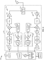
- FIG. 2 is a block diagram 200 of an exemplary wireless device, such as the wireless device 110.
- the wireless device includes a data processor / controller 210, a transceiver 218, and an antenna 290.
- the data processor / controller 210 may be referred to as a processing system.
- a processing system may include the data processor / controller 210 or both the data processor / controller 210 and the memory 216.
- the transceiver 218 includes a transmitter 220 and a receiver 250 that support bi-directional communication.
- the transmitter 220 and/or the receiver 250 may be implemented with a super-heterodyne architecture or a direct-conversion architecture.
- a signal is frequency converted between RF and baseband in multiple stages, e.g., from RF to an intermediate frequency (IF) in one stage, and then from IF to baseband in another stage for a receiver.
- IF intermediate frequency
- the direct-conversion architecture which is also referred to as a zero-IF architecture
- a signal is frequency converted between RF and baseband in one stage.
- the super-heterodyne and direct-conversion architectures may use different circuit blocks and/or have different requirements.
- the transmitter 220 and the receiver 250 are implemented with the direct-conversion architecture.
- the data processor / controller 210 may process (e.g., encode and modulate) data to be transmitted and provide the data to a digital-to-analog converter (DAC) 230.
- the DAC 230 converts a digital input signal to an analog output signal.
- the analog output signal is provided to a transmit (TX) baseband (lowpass) filter 232, which may filter the analog output signal to remove images caused by the prior digital-to-analog conversion by the DAC 230.
- An amplifier (amp) 234 may amplify the signal from the TX baseband filter 232 and provide an amplified baseband signal.
- An upconverter (mixer) 236 may receive the amplified baseband signal and a TX LO signal from a TX LO signal generator 276.
- the upconverter 236 may upconvert the amplified baseband signal with the TX LO signal and provide an upconverted signal.
- a filter 238 may filter the upconverted signal to remove images caused by the frequency upconversion.
- a power amplifier (PA) 240 may amplify the filtered RF signal from the filter 238 to obtain the desired output power level and provide an output RF signal.
- the output RF signal may be routed through a duplexer/switchplexer 264.
- the transmitter 220 and the receiver 250 may be coupled to the duplexer 264, which may include a TX filter for the transmitter 220 and a receive (RX) filter for the receiver 250.
- the TX filter may filter the output RF signal to pass signal components in a transmit band and attenuate signal components in a receive band.
- the transmitter 220 and the receiver 250 may be coupled to switchplexer 264.
- the switchplexer 264 may pass the output RF signal from the transmitter 220 to the antenna 290 during uplink time intervals.
- the duplexer/switchplexer 264 may provide the output RF signal to the antenna 290 for transmission via a wireless channel.
- the antenna 290 may receive signals transmitted by base stations and/or other transmitter stations and may provide a received RF signal.
- the received RF signal may be routed through duplexer/switchplexer 264.
- the RX filter within the duplexer 264 may filter the received RF signal to pass signal components in a receive band and attenuate signal components in the transmit band.
- the switchplexer 264 may pass the received RF signal from the antenna 290 to the receiver 250 during downlink time intervals.
- the duplexer/switchplexer 264 may provide the received RF signal to the receiver 250.
- the received RF signal may be amplified by a low noise amplifier (LNA) 252 and filtered by a filter 254 to obtain an input RF signal.
- a downconverter (mixer) 256 may receive the input RF signal and an RX LO signal from an RX LO signal generator 286. The downconverter 256 may downconvert the input RF signal with the RX LO signal and provide a downconverted signal.
- the downconverted signal may be amplified by an amplifier 258 and further filtered by an RX baseband (lowpass) filter 260 to obtain an analog input signal.
- the analog input signal is provided to an analog-to-digital converter (ADC) 262.
- the ADC 262 converts an analog input signal to a digital output signal.
- the digital output signal is provided to the data processor / controller 210.
- a TX frequency synthesizer 270 may include a TX phase locked loop (PLL) 272 and a VCO 274.
- the VCO 274 may generate a TX VCO signal at a desired frequency.
- the TX PLL 272 may receive timing information from the data processor / controller 210 and generate a control signal for the VCO 274.
- the control signal may adjust the frequency and/or the phase of the VCO 274 to obtain the desired frequency for the TX VCO signal.
- the TX frequency synthesizer 270 provides the TX VCO signal to the TX LO signal generator 276.
- the TX LO signal generator may generate a TX LO signal based on the TX VCO signal received from the TX frequency synthesizer 270.
- a RX frequency synthesizer 280 may include an RX PLL 282 and a VCO 284.
- the VCO 284 may generate an RX VCO signal at a desired frequency.
- the RX PLL 282 may receive timing information from the data processor / controller 210 and generate a control signal for the VCO 284.
- the control signal may adjust the frequency and/or the phase of the VCO 284 to obtain the desired frequency for the RX VCO signal.
- the RX frequency synthesizer 280 provides the RX VCO signal to the RX LO signal generator 286.
- the RX LO signal generator may generate an RX LO signal based on the RX VCO signal received from the RX frequency synthesizer 280.
- the LO signal generators 276, 286 may each include frequency dividers, buffers, etc.
- the LO signal generators 276, 286 may be referred to as frequency dividers if they divide a frequency provided by the TX frequency synthesizer 270 and the RX frequency synthesizer 280, respectively.
- the PLLs 272, 282 may each include a phase/frequency detector, a loop filter, a charge pump, a frequency divider, etc.
- Each VCO signal and each LO signal may be a periodic signal with a particular fundamental frequency.
- the TX LO signal and the RX LO signal from the LO signal generators 276, 286 may have the same frequency for TDD or different frequencies for FDD.
- the TX VCO signal and the RX VCO signal from the VCOs 274, 284 may have the same frequency (e.g., for TDD) or different frequencies (e.g., for FDD or TDD).
- the conditioning of the signals in the transmitter 220 and the receiver 250 may be performed by one or more stages of amplifier, filter, upconverter, downconverter, etc. These circuits may be arranged differently from the configuration shown in FIG. 2 . Furthermore, other circuits not shown in FIG. 2 may also be used to condition the signals in the transmitter 220 and the receiver 250. For example, impedance matching circuits may be located at the output of the PA 240, at the input of the LNA 252, between the antenna 290 and the duplexer/switchplexer 264, etc. Some circuits in FIG. 2 may also be omitted. For example, the filter 238 and/or the filter 254 may be omitted.
- All or a portion of the transceiver 218 may be implemented on one or more analog integrated circuits (ICs), RF ICs (RFICs), mixed-signal ICs, etc.
- ICs analog integrated circuits
- RFICs RF ICs
- the TX baseband filter 232 to the PA 240 in the transmitter 220, the LNA 252 to the RX baseband filter 260 in the receiver 250, the PLLs 272, 282, the VCOs 274, 284, and the LO signal generators 276, 286 may be implemented on an RFIC.
- the PA 240 and possibly other circuits may also be implemented on a separate IC or a circuit module.
- the data processor / controller 210 may perform various functions for the wireless device. For example, the data processor / controller 210 may perform processing for data being transmitted via the transmitter 220 and received via the receiver 250. The data processor / controller 210 may control the operation of various circuits within the transmitter 220 and the receiver 250.
- the memory 212 and/or the memory 216 may store program codes and data for the data processor / controller 210.
- the memory may be internal to the data processor / controller 210 (e.g., the memory 212) or external to the data processor / controller 210 (e.g., the memory 216).
- the memory may be referred to as a computer-readable medium.
- An oscillator 214 may generate a VCO signal at a particular frequency.
- a clock generator 215 may receive the VCO signal from the oscillator 214 and may generate clock signals for various modules within the data processor / controller 210.
- the data processor / controller 210 may be implemented on one or more application specific integrated circuits (ASICs) and/or other ICs.
- ASICs application specific integrated circuits
- Frequency dividers such as the frequency dividers in LO signal generators 276, 286, are used extensively for generating LO signals. There is a need for a programmable frequency divider for generating LO signals in multi-band cellular transceivers that meets stringent LO requirements such as small chip area, good phase noise requirement, and quadrature output.
- a VCO (e.g., VCO 274 or VCO 284 of FIG. 2 ) is sensitive to noise spikes and spurs.
- PMIC power management integrated circuit
- PSRR power supply rejection ratio
- a spur e.g., a spike
- an effective VCO regulator that is capable of providing a good bandwidth (e.g., a wide bandwidth) and attenuating the spur (e.g., the large spike) for the VCO.
- a wider PSRR bandwidth may provide improved performance of a VCO regulator
- increasing the PSRR bandwidth may also cause the noise bandwidth to increase. Therefore, there is a trade-off between increasing the PSRR bandwidth and increasing noise bandwidth that is not desirable.
- the VCO may implement a VCO regulator with a dual supply configuration to supply voltage.
- the dual supply configuration may alleviate supply/electromagnetic pulling of the VCO.
- the dual voltage supply configuration may supply high voltage (HV) for a GSM mode and may supply low voltage (LV) for a non-GSM mode (e.g., for CDMA, LTE, etc.).
- HV high voltage
- LV low voltage
- a specific LV PSRR for low voltage is a concern for satisfactory performance of a VCO regulator because the voltage supplied to the VCO regulator is low in the LV non-GSM mode.
- a VCO regulator should provide an LV PSRR of approximately 100dB in several hundreds KHz to MHz range with dropout voltage of less than 100mV.
- Example simulation results illustrate that for the LV non-GSM mode, a PSRR of approximately 100dB is desired at 100KHz to mitigate the PMIC PFM spurs.
- good noise performance is a concern for satisfactory performance of a VCO regulator because a high voltage supplied to the VCO regulator may increase the noise bandwidth.
- the VCO regulator provides a certain PSRR at a frequency of several tens of MHz range, while maintaining low noise for the high voltage.
- a VCO regulator be programmable (e.g., tunable) to satisfy various PSRR/noise specifications and to adapt to the tradeoff between the PSRR and the noise.
- the VCO regulator should be programmable to provide different PSRR and noise characteristics for different uses.
- the VCO regulator should be programmable to provide different PSRR and noise characteristics depending on whether the mode is the LV mode or the HV mode.
- performance of the VCO regulator is related to a type of a pass element (e.g., DC bias, input/output impedance).
- a type of a pass element e.g., DC bias, input/output impedance.
- NMOS N-type metal-oxide-semiconductor
- PMOS P-type metal-oxide-semiconductor
- Table 1 illustrates comparison between an NMOS regulator and a PMOS regulator.
- a number of plus signs (+) represents a degree of desirable performance
- a number of minus signs (-) represents a degree of undesirable performance.
- Table 1 Comparison between an NMOS regulator and a PMOS regulator Regulator type PSRR @low freq.
- the NMOS regulator according to the disclosure implements a two-stage operational transconductance amplifier (OTA) circuit to obtain a desirable PSRR (e.g., 100dB).
- the two-stage OTA circuit may limit the bandwidth to obtain 100dB at 100kHz via a compensation network.
- the compensation network in the two-stage OTA circuit also provides pole cancellation.
- FIG. 3 is an example circuit diagram 300 of an NMOS regulator according to the disclosure.
- the NMOS regulator 300 includes an NMOS 302.
- the NMOS 302 has a source (S), a drain (D), and a gate (G).
- the NMOS regulator 300 includes a first amplifier 304 and a second amplifier 306 to provide a two-stage OTA circuit.
- the second amplifier 306 may be a common source amplifier.
- a PSSR of 60-70 dB may be achieved in the first stage through the first amplifier 304, and a PSSR of 30-40dB may be achieved in the second stage through the second amplifier 306, thereby achieving a total PSSR of approximately 100dB for the two-stage OTA circuit.
- An output of the first amplifier 304 is connected to an input of the second amplifier 306, and the output of the second amplifier 306 is connected to the gate (G) of the NMOS 302.
- the output of the first amplifier 304 is also connected to a capacitor 308 with capacitance CM at a first end of the capacitor 308.
- a second end of the capacitor 308 is connected to a first end of a resistor 310 with resistance RM.
- a second end of the resistor 310 is connected to the source (S) of the NMOS 302 and a VCO 350.
- the VCO 350 may be equivalent to the VCO 274 or the VCO 284 of FIG. 2 .
- the capacitor 308 and the resistor 310 form a compensation network to compensate the regulator output 312 to the output of the first stage OTA circuit including the first amplifier 304.
- the capacitor 308 and the resistor 310 may be matched with transconductance (Gm) of the first stage OTA circuit.
- Gm transconductance
- the compensation network including the capacitor 308 and the resistor 310 may be tunable to match with the Gm of the first stage OTA circuit for stability and to minimize noise. It is noted that both the compensation network and the first stage OTA circuit are tunable to match with each other. Because at least one of the compensation network or the first stage OTA circuit is tunable, the regulator can maintain good stability, good regulator bandwidth, and lower noise. It is noted that, if the first stage OTA Gm is larger, the compensation network provides a stronger compensation, and thus provides better stability.
- a path is a gain through A path shown in FIG. 3 .
- s is j ⁇ .
- A is a DC gain from a supply to the regulator output 312.
- A2 is a DC gain at the second amplifier 306.
- ro 1 is output resistance of the first amplifier 304.
- ⁇ p 1 is a pole at the output of the first amplifier 304
- ⁇ p 2 is a pole at the output of the second amplifier 306,
- ⁇ p 3 is a pole at the output 312 of the NMOS regulator.
- ⁇ z is a zero generated by the compensation network with the resistor 310 and the capacitor 308.
- a LP is an open loop DC gain from the input of first amplifier 304 to the regulator output 312.
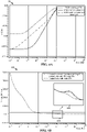
- FIG. 4A is an example PSSR plot 400 of PSSR values in various cases at a regulator.
- the PSSR plot 400 illustrates that the pole cancellation (PC) 2-stage OTA regulator circuit provides a PSSR plot that is closer to the desirable PSSR of - 100 dB than the PSSR plots of a 1-stage OTA regulator and a conventional 2-stage OTA regulator.
- the pole cancellation provided by the 2-stage OTA regulator circuit of the disclosure e.g., via the NMOS regulator of FIG. 3 ) helps extend the bandwidth of the PSSR.
- FIG. 4B is an example noise plot 450 of noise values in various cases.
- the noise plot of the PC 2-stage OTA regulator circuit is similar to the noise plots of a 1-stage OTA regulator and a conventional 2-stage OTA regulator, except for a portion 452.
- the portion 452 of the example noise plot 450 is zoomed to a zoomed portion 454.
- the zoomed portion 454 indicates that both the PC 2-stage OTA regulator circuit and the conventional 2-stage OTA regular circuit experience slightly higher noise than the 1-stage OTA regular circuit.
- FIG. 5 is an example implementation circuit 500 of the NMOS regulator according to the disclosure.
- the NMOS regulator 500 includes a two-stage OTA circuit 502 including two OTAs and a compensation network including a resistor and a capacitor.
- the two-stage OTA circuit 502 may be equivalent to the two-stage OTA circuit including the first amplifier 304 and the second amplifier 306 in FIG. 3 .
- the compensation network 504 may be equivalent to the compensation network including the capacitor 308 and the resistor 310 in FIG. 3 .
- the compensation network 504 may be tunable to match with a first stage OTA circuit of the two-stage OTA circuit 502.
- a regulator circuit is a complementary metal-oxide-semiconductor (CMOS) regulator circuit that includes a PMOS regulator and an NMOS regulator, where the NMOS regulator is coupled to the PMOS regulator.
- the PMOS regulator may be connected to the NMOS regulator in series (in cascode).
- the PMOS regulator may be connected to the NMOS regulator in parallel.
- the regulator circuit is connected to a switch circuit to selectively choose an HV mode or an LV mode for the CMOS regulator circuit.
- the HV mode may be used for better performance in terms of less pulling effect and better phase noise performance.
- the HV mode may cause higher power consumption.
- the LV mode generally causes lower power consumption than the HV mode.
- the switch circuit may select the HV mode for the PMOS regulator and bypass the NMOS regulator. In another aspect, for the LV mode, the switch circuit may select either the NMOS regulator and bypass the PMOS regulator, or may select both the PMOS regulator and the NMOS regulator. In addition, it is noted that the PMOS regulator and the NMOS regulator have different input impedance and output impedance. The PMOs regulator generally has lower input impedance and higher output impedance than the NMOS regulator. Thus, in one aspect, the switch circuit may be used to select either the PMOS regulator or the NMOS regulator, depending on whether the VCO is an aggressor or a victim to surrounding building blocks.
- EM electromagnetic
- the switch circuit may select the PMOS regulator if the VCO is an aggressor that may affect the surrounding building blocks (e.g., by pulling the surrounding building blocks).
- the switch circuit may select the NMOS regulator if the VCO is a victim that may be affected by the surrounding building blocks (e.g., by being pulled by the surrounding building blocks). It is further noted that selecting both the PMOS regulator and the NMOS regulator that are connected in series would also provide isolation from affecting and/or being affected from the surrounding building blocks.
- FIGs. 6A-6B are example structures of a CMOS regulator.
- FIG. 6A is an example structure 600 of a CMOS regulator where a PMOS regulator 604 and an NMOS regulator 606 are connected in series.
- a switch circuit 602 is connected to the PMOS regulator 604 that is connected to the NMOS regulator 606 in series.
- the switch circuit 602 is configured to select one of an LV mode and an HV mode. As discussed supra, for example, the LV mode is used to supply low voltage for a non-GSM mode, and the HV mode is used to supply high voltage for a GSM mode.
- the order of the PMOS regulator 604 and the NMOS regulator 606 may be different from the example structure 600 of FIG. 6A .
- the CMOS regulator includes a PMOS regulator and an NMOS regulator.
- FIG. 6B is an example structure 650 of a CMOS regulator where a PMOS regulator 654 and an NMOS regulator 658 are connected in parallel.
- a first switch circuit 652 is connected to the PMOS regulator 654 and a second switch circuit 656 is connected to the NMOS regulator 658, where the PMOS regulator 654 and the NMOS regulator 658 are connected in parallel.
- the LV mode is used to supply low voltage for a non-GSM mode
- the HV mode is used to supply high voltage for a GSM mode.
- both the first switch circuit 652 and the second switch circuit 656 are configured to provide low voltage.
- both the first switch circuit 652 and the second switch circuit 656 are configured to provide high voltage.
- FIG. 7 is an example circuit diagram 700 including a cascode CMOS regulator.
- a switch circuit 710 is connected to a CMOS regulator that includes a PMOS regulator 730 and an NMOS regulator 750, where the PMOS regulator 730 and the NMOS regulator 750 are connected in series (cascode).
- the CMOS regulator is connected to a VCO circuit 770 via the NMOS regulator 750.
- the VCO circuit 770 may be equivalent to the VCO 274 or the VCO 284 of FIG. 2 .
- the VCO circuit 770 may have a low frequency (LF) VCO output at 772 and a high frequency (HF) VCO output at 774.
- LF low frequency
- HF high frequency
- the switch circuit 710 may selectively supply either a voltage of an HV mode or a voltage of an LV mode for the CMOS regulator.
- the switch circuit 710 may supply the HV mode voltage of 1.6V or the LV mode voltage of 0.95V to the CMOS regulator.
- the switch circuit 710 may selectively supply either a voltage of the HV mode or a voltage of the LV mode depending on various factors such as following.
- the HV mode may provide better VCO phase noise and swing as well as better VCO buffer phase noise and swing than the LV mode.
- the LV mode may cause lower power consumption than the HV mode.
- the supply voltage domain of the voltage supplied to the CMOS regulator may be configured to experience less supply coupling. It is also noted that the VCO is less sensitive to EM coupling in the HV mode than in the LV mode.
- the NMOS regulator 750 has a better PSRR at 100MHz than the PMOS regulator 730.
- the PMOS regulator 730 may have better noise performance (e.g., lower noise) at 100MHz (e.g., in GSM, HV and low PMOS regulator BW) than the NMOS regulator 750.
- the NMOS regulator 750 can achieve a PSRR of 100dB at 1MHz with 100mV drop-out.
- the NMOS regulator 750 has a two-stage OTA and pole cancellation features to achieve a PSRR of 100dB at 1MHz for PFM spurs.
- FIG. 8 is an example circuit diagram 800 including a buffer circuit.
- a switch circuit 810 is connected to a buffer circuit 830.
- the switch circuit 810 may selectively provide either an HV mode or an LV mode.
- the buffer circuit 830 receives outputs from the VCO, such as the VCO circuit 770 of FIG. 7 , and buffers the outputs.
- the buffer circuit 830 may be connected to the VCO circuit 770 of FIG. 7 .
- the LF VCO input 832 into the buffer circuit 830 may be from the LF VCO output 772 of FIG. 7
- the HF VCO input 834 into the buffer circuit 830 may be from the HF VCO output 774 of FIG. 7 .
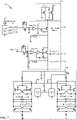
- FIG. 9 is an example circuit structure 900 at a system level according to the disclosure.
- the example circuit structure 900 includes a transmission (TX) VCO regulator 902, a first reception (RX) carrier aggregation (CA) regulator 904, and a second RX CA regulator 906.
- the first RX CA regulator 904 is for receiving carrier aggregation at a first frequency
- the second RX CA regulator 906 is for receiving carrier aggregation at a second frequency.
- Each one of the TX VCO regulator 902, the first RX CA regulator 904, and the second RX CA regulator 906 includes a CMOS regulator structure having a PMOS regulator coupled to an NMOS regulator.
- FIG. 10A is an example PSSR plot 1000 of PSSR values in various cases at a VCO.
- the PSSR plot 1000 illustrates that a 2-stage OTA regulator circuit provides a PSSR plot for the VCO that is closer to the desirable PSSR of -100 dB than the PSSR plots of a 1-stage OTA regulator.
- the PSRR of 100 dB at 100kHZ is achieved by the 2-stage OTA regulator.
- the VCO may also experience 50 dB improvement when the 2-stage OTA regulator is used.
- FIG. 10B is an example noise plot 1050 of noise values in various cases at a VCO.
- the noise plot of the 1-stage OTA regulator has spurs 1052 and 1054, whereas the noise plot of a 2-stage OTA regulator does not have spurs.
- the VCO experiences spur reduction when the 2-stage OTA regulator is used.
- 4-5 dB reference side band (RSB) improvement may be provided.
- FIG. 11 is a flow chart 1100 of a method by a regulator circuit.
- the method may be performed by a regulator circuit (e.g., the regulator circuit 600, 650, the apparatus 1202/1202').
- the regulator circuit regulates, via a first voltage regulator, a first input voltage to the first voltage regulator, the first voltage regulator including a PMOS.
- the regulator circuit regulates, via a second voltage regulator, a second input voltage to the second voltage regulator, the second voltage regulator including an NMOS, where the first voltage regulator is connected to the second voltage regulator.
- the regulator circuit selectively activates, via a switch circuit, at least one of the first voltage regulator or the second voltage regulator. In an aspect, the at least one of the first voltage regulator or the second voltage regulator is selectively activated based on noise.
- FIG. 12 is a conceptual data flow diagram 1200 illustrating the data flow between different modules/means/components in an exemplary apparatus 1202.
- the apparatus may be a regulator circuit.
- the apparatus includes a first voltage regulator module 1204, a second voltage regulator module 1206, and a switching module 1208.
- the first voltage regulator module 1204 regulates a first input voltage to the first voltage regulator module 1204.
- the first voltage regulator module 1204 includes a PMOS.
- the second voltage regulator module 1206 regulates a second input voltage to the second voltage regulator module 1206.
- the second voltage regulator module 1206 includes an NMOS.
- the first voltage regulator is connected to the second voltage regulator.
- the switching module 1208 selectively activates at least one of the first voltage regulator module 1204 or the second voltage regulator module 1206.
- the at least one of the first voltage regulator module 1204 or the second voltage regulator 1206 is selectively activated based on noise.
- the apparatus may include additional modules that perform each of the blocks of the algorithm in the aforementioned flow charts of FIG. 11 .
- each block in the aforementioned flow charts of FIG. 11 may be performed by a module and the apparatus may include one or more of those modules.
- the modules may be one or more hardware components specifically configured to carry out the stated processes/algorithm, implemented by a processor configured to perform the stated processes/algorithm, stored within a computer-readable medium for implementation by a processor, or some combination thereof.
- FIG. 13 is a diagram 1300 illustrating an example of a hardware implementation for an apparatus 1202' employing a processing system 1314.
- the processing system 1314 may be implemented with a bus architecture, represented generally by the bus 1324.
- the bus 1324 may include any number of interconnecting buses and bridges depending on the specific application of the processing system 1314 and the overall design constraints.
- the bus 1324 links together various circuits including one or more processors and/or hardware modules, represented by the processor 1304, the modules 1204, 1206, 1208, and the computer-readable medium / memory 1306.
- the bus 1324 may also link various other circuits such as timing sources, peripherals, voltage regulators, and power management circuits, which are well known in the art, and therefore, will not be described any further.
- the processing system 1314 may be coupled to a transceiver 1310.
- the transceiver 1310 is coupled to one or more antennas 1320.
- the transceiver 1310 provides a means for communicating with various other apparatus over a transmission medium.
- the transceiver 1310 receives a signal from the one or more antennas 1320, extracts information from the received signal, and provides the extracted information to the processing system 1314.
- the transceiver 1310 receives information from the processing system 1314, and based on the received information, generates a signal to be applied to the one or more antennas 1320.
- the processing system 1314 includes a processor 1304 coupled to a computer-readable medium / memory 1306.
- the processor 1304 is responsible for general processing, including the execution of software stored on the computer-readable medium / memory 1306.
- the software when executed by the processor 1304, causes the processing system 1314 to perform the various functions described supra for any particular apparatus.
- the computer-readable medium / memory 1306 may also be used for storing data that is manipulated by the processor 1304 when executing software.
- the processing system further includes at least one of the modules 1204, 1206, and 1208.
- the modules may be software modules running in the processor 1304, resident/stored in the computer readable medium / memory 1306, one or more hardware modules coupled to the processor 1304, or some combination thereof.
- the apparatus 1202/1202' includes means for regulating a first input voltage to the means for regulating the first input voltage, the means for regulating the first input voltage including a PMOS, means for regulating a second input voltage to the means for regulating the second voltage, the means for regulating the second voltage including an NMOS, where the means for regulating the first input voltage is connected to the means for regulating the second voltage, and means for selectively activating at least one of the means for regulating the first input voltage or the means for regulating the second voltage.
- the means for selectively activating is configured to selectively activate at least one of the means for regulating the first input voltage or the means for regulating the second voltage based on noise.
- the aforementioned means may be one or more of the aforementioned modules of the apparatus 1202 and/or the processing system 1314 of the apparatus 1202' configured to perform the functions recited by the aforementioned means.
Landscapes
- Engineering & Computer Science (AREA)
- Physics & Mathematics (AREA)
- Electromagnetism (AREA)
- General Physics & Mathematics (AREA)
- Radar, Positioning & Navigation (AREA)
- Automation & Control Theory (AREA)
- Power Engineering (AREA)
- Amplifiers (AREA)
- Continuous-Control Power Sources That Use Transistors (AREA)
- Semiconductor Integrated Circuits (AREA)
- Transceivers (AREA)
Claims (9)
- Circuit régulateur CMOS à oscillateur commandé en tension, VCO, (600, 650, 700) comprenant un régulateur CMOS qui est connectable à un VCO (770), le régulateur CMOS comportant :un premier régulateur de tension (604, 654, 730) configuré pour réguler une première tension d'entrée fournie au premier régulateur de tension (604, 654, 730), le premier régulateur de tension (604, 654, 730) comportant un élément de transmission métal-oxyde-semiconducteur de type P, PMOS ;un deuxième régulateur de tension (606, 658, 750) configuré pour réguler une deuxième tension d'entrée fournie au deuxième régulateur de tension (606, 658, 750), le deuxième régulateur de tension (606, 658, 750) comportant un élément de transmission métal-oxyde-semiconducteur de type N, NMOS, dans lequel le premier régulateur de tension (604, 654, 730) est connecté au deuxième régulateur de tension (606, 658, 750) ;caractérisé en ce que le circuit régulateur CMOS à VCO (600, 650, 700) comprend en outre :un circuit de commutation (602, 652, 656, 710) connecté au régulateur CMOS, le circuit de commutation (602, 652, 656, 710) étant configuré pour sélectionner un mode de tension en sélectionnant soit un mode haute tension, HV, soit un mode basse tension, LV, pour le régulateur CMOS, et pour activer sélectivement au moins un parmi le premier régulateur de tension (604, 654, 730) et le deuxième régulateur de tension (606, 658, 750) dans le mode de tension sélectionné,dans lequel le circuit de commutation (602, 652, 656, 710) est configuré pour sélectionner le mode HV sur la base des effets d'élévation du VCO (770) connectable au circuit régulateur CMOS à VCO (600, 650, 700) et pour activer sélectivement l'au moins un parmi le premier régulateur de tension (604, 654, 730) et le deuxième régulateur de tension (606, 658, 750) sur la base des effets d'élévation.
- Circuit régulateur CMOS à VCO (600, 650, 700) selon la revendication 1, dans lequel le premier régulateur de tension (604, 654, 730) et le deuxième régulateur de tension (606, 658, 750) sont connectés en série.
- Circuit régulateur CMOS à VCO (600, 650, 700) selon la revendication 1, dans lequel le premier régulateur de tension (604, 654, 730) et le deuxième régulateur de tension (606, 658, 750) sont connectés en parallèle.
- Circuit régulateur CMOS à VCO selon la revendication 1, dans lequel le premier régulateur de tension (604, 654, 730) comporte un circuit amplificateur à deux étages configuré pour amplifier la première tension d'entrée dans deux étages.
- Circuit régulateur CMOS à VCO selon la revendication 1, dans lequel le deuxième régulateur de tension (606, 658, 750) comporte un circuit amplificateur à deux étages configuré pour amplifier la deuxième tension d'entrée dans deux étages.
- Circuit régulateur CMOS à VCO selon la revendication 1, dans lequel le deuxième régulateur de tension (606, 658, 750) comporte un circuit d'annulation de pôle.
- Circuit régulateur CMOS à VCO selon la revendication 1, dans lequel le deuxième régulateur de tension (606, 658, 750) comporte un condensateur et une résistance, et dans lequel une extrémité de la résistance est connectée au condensateur et une autre extrémité de la résistance est connectée à une source de l'élément de transmission NMOS et dans lequel une autre extrémité du condensateur est connectée à une grille de l'élément de transmission NMOS.
- Circuit régulateur CMOS à VCO selon la revendication 1, dans lequel le premier régulateur de tension (604, 654, 730) et le deuxième régulateur de tension (606, 658, 750) ont une impédance d'entrée et une impédance de sortie différentes.
- Procédé (1110) mis en œuvre par un circuit régulateur CMOS à oscillateur commandé en tension, VCO, (600, 650, 700) comprenant un régulateur CMOS qui est connectable à un VCO (770), le régulateur CMOS comportant un premier régulateur de tension (604, 654, 730) et un deuxième régulateur de tension (606, 658, 750), le procédé (1100) comprenant :la régulation (1102), par l'intermédiaire du premier régulateur de tension (604, 654, 730), d'une première tension d'entrée fournie au premier régulateur de tension (604, 654, 730), le premier régulateur de tension (604, 654, 730) comportant un élément de transmission métal-oxyde-semiconducteur de type P, PMOS ;la régulation (1104), par l'intermédiaire du deuxième régulateur de tension (606, 658, 750), d'une deuxième tension d'entrée fournie au deuxième régulateur de tension (606, 658, 750), le deuxième régulateur de tension (606, 658, 750) comportant un élément de transmission métal-oxyde-semiconducteur de type N, NMOS, dans lequel le premier régulateur de tension (604, 654, 730) est connecté au deuxième régulateur de tension (606, 658, 750) ;caractérisé en ce qu'il comprend en outre :la sélection d'un mode de tension, par l'intermédiaire d'un circuit de commutation (602, 652, 656, 710) compris en outre dans le régulateur de tension CMOS à VCO (600, 650, 700) et couplé au régulateur CMOS, en sélectionnant soit un mode haute tension, HV, soit un mode basse tension, LV, pour le régulateur CMOS, et l'activation sélective (1106) d'au moins un parmi le premier régulateur de tension (604, 654, 730) et le deuxième régulateur de tension (606, 658, 750) sur la base du mode de tension sélectionné,dans lequel le mode HV est sélectionné sur la base des effets d'élévation du VCO connectable au circuit régulateur CMOS à VCO (600, 650, 700) et l'au moins un parmi le premier régulateur de tension (604, 654, 730) et le deuxième régulateur de tension (606, 658, 750) est sélectionné sur la base des effets d'élévation.
Priority Applications (1)
| Application Number | Priority Date | Filing Date | Title |
|---|---|---|---|
| EP22197509.7A EP4130925A1 (fr) | 2014-05-30 | 2015-05-15 | Régulateurs cmos multimodes à double alimentation sur puce |
Applications Claiming Priority (3)
| Application Number | Priority Date | Filing Date | Title |
|---|---|---|---|
| US201462005765P | 2014-05-30 | 2014-05-30 | |
| US14/630,506 US11095216B2 (en) | 2014-05-30 | 2015-02-24 | On-chip dual-supply multi-mode CMOS regulators |
| PCT/US2015/030948 WO2015183588A1 (fr) | 2014-05-30 | 2015-05-15 | Régulateurs cmos multimodes à double alimentation sur puce |
Related Child Applications (2)
| Application Number | Title | Priority Date | Filing Date |
|---|---|---|---|
| EP22197509.7A Division EP4130925A1 (fr) | 2014-05-30 | 2015-05-15 | Régulateurs cmos multimodes à double alimentation sur puce |
| EP22197509.7A Division-Into EP4130925A1 (fr) | 2014-05-30 | 2015-05-15 | Régulateurs cmos multimodes à double alimentation sur puce |
Publications (2)
| Publication Number | Publication Date |
|---|---|
| EP3149553A1 EP3149553A1 (fr) | 2017-04-05 |
| EP3149553B1 true EP3149553B1 (fr) | 2022-11-23 |
Family
ID=53284554
Family Applications (2)
| Application Number | Title | Priority Date | Filing Date |
|---|---|---|---|
| EP15727151.1A Active EP3149553B1 (fr) | 2014-05-30 | 2015-05-15 | Régulateurs cmos multimodes à double alimentation sur puce |
| EP22197509.7A Pending EP4130925A1 (fr) | 2014-05-30 | 2015-05-15 | Régulateurs cmos multimodes à double alimentation sur puce |
Family Applications After (1)
| Application Number | Title | Priority Date | Filing Date |
|---|---|---|---|
| EP22197509.7A Pending EP4130925A1 (fr) | 2014-05-30 | 2015-05-15 | Régulateurs cmos multimodes à double alimentation sur puce |
Country Status (7)
| Country | Link |
|---|---|
| US (2) | US11095216B2 (fr) |
| EP (2) | EP3149553B1 (fr) |
| JP (1) | JP6522666B2 (fr) |
| KR (1) | KR20170013248A (fr) |
| CN (1) | CN106462175B (fr) |
| BR (1) | BR112016028170A2 (fr) |
| WO (1) | WO2015183588A1 (fr) |
Families Citing this family (13)
| Publication number | Priority date | Publication date | Assignee | Title |
|---|---|---|---|---|
| US11095216B2 (en) * | 2014-05-30 | 2021-08-17 | Qualcomm Incorporated | On-chip dual-supply multi-mode CMOS regulators |
| US9588541B1 (en) | 2015-10-30 | 2017-03-07 | Qualcomm Incorporated | Dual loop regulator circuit |
| US9946283B1 (en) | 2016-10-18 | 2018-04-17 | Qualcomm Incorporated | Fast transient response low-dropout (LDO) regulator |
| US10411599B1 (en) | 2018-03-28 | 2019-09-10 | Qualcomm Incorporated | Boost and LDO hybrid converter with dual-loop control |
| US10444780B1 (en) | 2018-09-20 | 2019-10-15 | Qualcomm Incorporated | Regulation/bypass automation for LDO with multiple supply voltages |
| US10591938B1 (en) | 2018-10-16 | 2020-03-17 | Qualcomm Incorporated | PMOS-output LDO with full spectrum PSR |
| US10545523B1 (en) | 2018-10-25 | 2020-01-28 | Qualcomm Incorporated | Adaptive gate-biased field effect transistor for low-dropout regulator |
| KR20200145968A (ko) | 2019-06-21 | 2020-12-31 | 삼성전자주식회사 | 적은 노이즈를 포함하는 전압을 출력하도록 구성되는 증폭 회로를 구성하기 위한 전자 회로 |
| US11372436B2 (en) | 2019-10-14 | 2022-06-28 | Qualcomm Incorporated | Simultaneous low quiescent current and high performance LDO using single input stage and multiple output stages |
| US11429129B2 (en) * | 2020-05-13 | 2022-08-30 | Sensata Technologies, Inc. | Multi-deck circuits with common rails |
| US11280847B1 (en) * | 2020-10-30 | 2022-03-22 | Taiwan Semiconductor Manufacturing Company Ltd. | Circuit, semiconductor device and method for parameter PSRR measurement |
| US11803204B2 (en) * | 2021-04-23 | 2023-10-31 | Qualcomm Incorporated | Low-dropout (LDO) voltage regulator with voltage droop compensation circuit |
| KR20220169850A (ko) * | 2021-06-21 | 2022-12-28 | 에스케이하이닉스 주식회사 | 파워스위칭동작을 수행하는 전자장치 |
Citations (3)
| Publication number | Priority date | Publication date | Assignee | Title |
|---|---|---|---|---|
| US7064531B1 (en) * | 2005-03-31 | 2006-06-20 | Micrel, Inc. | PWM buck regulator with LDO standby mode |
| US20070018625A1 (en) * | 2005-07-21 | 2007-01-25 | Oki Electric Industry Co., Ltd. | Voltage regulator |
| US20100045249A1 (en) * | 2008-08-19 | 2010-02-25 | Sun Microsystems, Inc. | Voltage regulator for write/read assist circuit |
Family Cites Families (56)
| Publication number | Priority date | Publication date | Assignee | Title |
|---|---|---|---|---|
| US5336986A (en) * | 1992-02-07 | 1994-08-09 | Crosspoint Solutions, Inc. | Voltage regulator for field programmable gate arrays |
| JP2839819B2 (ja) * | 1993-05-28 | 1998-12-16 | 株式会社東芝 | 不揮発性半導体記憶装置 |
| US5528127A (en) | 1994-05-17 | 1996-06-18 | National Semiconductor Corporation | Controlling power dissipation within a linear voltage regulator circuit |
| JP2001159921A (ja) | 1999-12-03 | 2001-06-12 | Seiko Epson Corp | 電源回路 |
| JP2001282371A (ja) | 2000-03-31 | 2001-10-12 | Seiko Instruments Inc | ボルテージレギュレータ |
| US6515880B1 (en) * | 2001-10-19 | 2003-02-04 | Texas Instruments Incorporated | Soft-start control for DC/DC switching regulators |
| US6677735B2 (en) | 2001-12-18 | 2004-01-13 | Texas Instruments Incorporated | Low drop-out voltage regulator having split power device |
| DE10215084A1 (de) | 2002-04-05 | 2003-10-30 | Infineon Technologies Ag | Schaltungsanordnung zur Spannungsregelung |
| EP1437638B1 (fr) | 2002-12-17 | 2016-02-24 | Infineon Technologies AG | Circuit pour générer une tension d' alimentation |
| DE10334066A1 (de) | 2003-07-25 | 2005-02-24 | Infineon Technologies Ag | Schaltungsanordnung zur Spannungsregelung und Verfahren zum Betreiben einer Schaltunsanordnung zur Spannugsregelung |
| US7161339B2 (en) | 2003-08-20 | 2007-01-09 | Broadcom Corporation | High voltage power management unit architecture in CMOS process |
| US6894472B2 (en) | 2003-08-20 | 2005-05-17 | Broadcom Corporation | Low leakage CMOS power mux |
| US6879142B2 (en) | 2003-08-20 | 2005-04-12 | Broadcom Corporation | Power management unit for use in portable applications |
| US7145370B2 (en) * | 2003-09-05 | 2006-12-05 | Impinj, Inc. | High-voltage switches in single-well CMOS processes |
| US7177182B2 (en) * | 2004-03-30 | 2007-02-13 | Impinj, Inc. | Rewriteable electronic fuses |
| US6979983B2 (en) | 2004-04-28 | 2005-12-27 | Faraday Technology Corp. | Voltage regulator |
| US7268993B2 (en) | 2004-05-25 | 2007-09-11 | Sbc Knowledge Ventures, L.P. | Integrated protector and splitter |
| JP4396402B2 (ja) * | 2004-06-03 | 2010-01-13 | ソニー株式会社 | 定電圧電源回路 |
| JP4094045B2 (ja) * | 2004-09-08 | 2008-06-04 | 富士通株式会社 | Pll周波数シンセサイザ |
| EP1669831A1 (fr) | 2004-12-03 | 2006-06-14 | Dialog Semiconductor GmbH | Étape de sortie d'un régulateur de voltage avec transistors MOS à basse tension |
| US7071664B1 (en) | 2004-12-20 | 2006-07-04 | Texas Instruments Incorporated | Programmable voltage regulator configurable for double power density and reverse blocking |
| US7106032B2 (en) | 2005-02-03 | 2006-09-12 | Aimtron Technology Corp. | Linear voltage regulator with selectable light and heavy load paths |
| US7253663B2 (en) | 2005-06-15 | 2007-08-07 | Ati Technologies Inc. | Apparatus and methods for self-biasing differential signaling circuitry having multimode output configurations for low voltage applications |
| US20070002596A1 (en) | 2005-06-29 | 2007-01-04 | Eaton Corporation | Two-stage, wide range power supply for a network protector control relay |
| US7199565B1 (en) | 2006-04-18 | 2007-04-03 | Atmel Corporation | Low-dropout voltage regulator with a voltage slew rate efficient transient response boost circuit |
| US7531996B2 (en) | 2006-11-21 | 2009-05-12 | System General Corp. | Low dropout regulator with wide input voltage range |
| US7583116B2 (en) * | 2007-08-03 | 2009-09-01 | International Business Machines Corporation | High output resistance, wide swing charge pump |
| US7548093B1 (en) * | 2008-03-05 | 2009-06-16 | Freescale Semiconductor, Inc. | Scheme of level shifter cell |
| TWI355801B (en) | 2008-04-01 | 2012-01-01 | Richtek Technology Corp | Dual power switch and voltage regulator using same |
| US7952900B2 (en) * | 2008-04-16 | 2011-05-31 | Analog Devices, Inc. | H-bridge buck-boost converter |
| US8305056B2 (en) * | 2008-12-09 | 2012-11-06 | Qualcomm Incorporated | Low drop-out voltage regulator with wide bandwidth power supply rejection ratio |
| US7994759B2 (en) * | 2009-04-13 | 2011-08-09 | Himax Technologies Limited | System and method for driving a power supply device in an initial activation stage |
| JP2010252094A (ja) * | 2009-04-16 | 2010-11-04 | Renesas Electronics Corp | Pll回路 |
| US7961056B2 (en) | 2009-09-10 | 2011-06-14 | Intel Corporation | Low phase noise voltage controlled oscillator |
| EP2354881A1 (fr) | 2010-02-05 | 2011-08-10 | Dialog Semiconductor GmbH | Régulateur de tension de domino |
| WO2011099965A1 (fr) | 2010-02-10 | 2011-08-18 | Skyworks Solutions, Inc. | Régulateur d'alimentation électrique multimode pour commande d'amplificateur de puissance |
| US8774739B2 (en) * | 2010-02-10 | 2014-07-08 | Skyworks Solutions, Inc. | Multi-mode power supply regulator for power amplifier control |
| US8519771B1 (en) | 2010-12-22 | 2013-08-27 | Xilinx, Inc. | Methods and apparatus for receiving high and low voltage signals using a low supply voltage technology |
| CN102096434B (zh) * | 2010-12-23 | 2012-11-28 | 东南大学 | 一种基于大摆率误差放大器的高精度高速ldo电路 |
| US8373446B2 (en) * | 2010-12-28 | 2013-02-12 | Texas Instruments Incorporated | Power supply detection circuit |
| JP2012147648A (ja) | 2011-01-14 | 2012-08-02 | Sony Corp | 電源制御装置および電源制御方法 |
| WO2013009418A1 (fr) | 2011-07-08 | 2013-01-17 | Rambus Inc. | Émetteur-récepteur empilé à grande vitesse et à faible puissance |
| CN102354245B (zh) | 2011-08-05 | 2013-06-12 | 电子科技大学 | 一种带隙电压基准源 |
| US8476940B2 (en) | 2011-12-02 | 2013-07-02 | Stmicroelectronics International N.V. | Stress reduced cascoded CMOS output driver circuit |
| US20130169246A1 (en) | 2011-12-28 | 2013-07-04 | Skymedi Corporation | Linear voltage regulating circuit adaptable to a logic system |
| CN102609023B (zh) | 2012-03-12 | 2013-11-20 | 北京经纬恒润科技有限公司 | 一种内建模拟电源电路 |
| US8890610B2 (en) * | 2012-03-28 | 2014-11-18 | Texas Instruments Incorporated | Compensation circuitry and method for amplifiers driving large capacitive loads |
| JP6004836B2 (ja) * | 2012-08-22 | 2016-10-12 | ルネサスエレクトロニクス株式会社 | 電源装置、半導体装置、及びワイヤレス通信装置 |
| US8981739B2 (en) * | 2012-09-26 | 2015-03-17 | Nxp B.V. | Low power low dropout linear voltage regulator |
| JP6211822B2 (ja) * | 2012-09-28 | 2017-10-11 | 旭化成エレクトロニクス株式会社 | 電力供給回路 |
| US9170590B2 (en) | 2012-10-31 | 2015-10-27 | Qualcomm Incorporated | Method and apparatus for load adaptive LDO bias and compensation |
| US9235225B2 (en) | 2012-11-06 | 2016-01-12 | Qualcomm Incorporated | Method and apparatus reduced switch-on rate low dropout regulator (LDO) bias and compensation |
| US8890499B2 (en) | 2013-03-11 | 2014-11-18 | Micrel, Inc. | Buck DC-DC converter with improved accuracy |
| CN103647449B (zh) | 2013-12-18 | 2016-08-17 | 嘉兴中润微电子有限公司 | 一种升压型电荷泵电路 |
| US9231525B2 (en) * | 2014-02-28 | 2016-01-05 | Google Inc. | Compensating a two stage amplifier |
| US11095216B2 (en) * | 2014-05-30 | 2021-08-17 | Qualcomm Incorporated | On-chip dual-supply multi-mode CMOS regulators |
-
2015
- 2015-02-24 US US14/630,506 patent/US11095216B2/en active Active
- 2015-05-15 CN CN201580028351.6A patent/CN106462175B/zh active Active
- 2015-05-15 EP EP15727151.1A patent/EP3149553B1/fr active Active
- 2015-05-15 JP JP2016569919A patent/JP6522666B2/ja active Active
- 2015-05-15 BR BR112016028170A patent/BR112016028170A2/pt not_active Application Discontinuation
- 2015-05-15 WO PCT/US2015/030948 patent/WO2015183588A1/fr active Application Filing
- 2015-05-15 KR KR1020167033178A patent/KR20170013248A/ko unknown
- 2015-05-15 EP EP22197509.7A patent/EP4130925A1/fr active Pending
-
2021
- 2021-07-20 US US17/443,093 patent/US11726513B2/en active Active
Patent Citations (3)
| Publication number | Priority date | Publication date | Assignee | Title |
|---|---|---|---|---|
| US7064531B1 (en) * | 2005-03-31 | 2006-06-20 | Micrel, Inc. | PWM buck regulator with LDO standby mode |
| US20070018625A1 (en) * | 2005-07-21 | 2007-01-25 | Oki Electric Industry Co., Ltd. | Voltage regulator |
| US20100045249A1 (en) * | 2008-08-19 | 2010-02-25 | Sun Microsystems, Inc. | Voltage regulator for write/read assist circuit |
Also Published As
| Publication number | Publication date |
|---|---|
| US20210351696A1 (en) | 2021-11-11 |
| KR20170013248A (ko) | 2017-02-06 |
| JP6522666B2 (ja) | 2019-05-29 |
| US20150349622A1 (en) | 2015-12-03 |
| EP4130925A1 (fr) | 2023-02-08 |
| EP3149553A1 (fr) | 2017-04-05 |
| US11726513B2 (en) | 2023-08-15 |
| CN106462175A (zh) | 2017-02-22 |
| US11095216B2 (en) | 2021-08-17 |
| BR112016028170A2 (pt) | 2017-08-22 |
| WO2015183588A1 (fr) | 2015-12-03 |
| JP2017517073A (ja) | 2017-06-22 |
| CN106462175B (zh) | 2018-03-16 |
Similar Documents
| Publication | Publication Date | Title |
|---|---|---|
| US11726513B2 (en) | On-chip dual-supply multi-mode CMOS regulators | |
| CN107078693B (zh) | 为混频器提供谐波响应抑制的电路 | |
| US9106234B2 (en) | Programmable frequency divider for local oscillator generation | |
| CN107580755B (zh) | 具有对供电电压的受控灵敏度的环形振荡器架构 | |
| US8988158B2 (en) | Hybrid voltage controlled oscillator | |
| CN107005230B (zh) | 用于从单端晶体振荡器生成四倍参考时钟的装置和方法 | |
| US8138844B1 (en) | System and method for crystal oscillator frequency tuning | |
| US9529380B1 (en) | Local oscillator signal generation circuit with harmonic current rejection | |
| US9209771B1 (en) | EM coupling shielding | |
| US9608569B2 (en) | Linearizing scheme for baseband filter with active feedback | |
| US20160099729A1 (en) | Apparatus and method for quadrupling frequency of reference clock |
Legal Events
| Date | Code | Title | Description |
|---|---|---|---|
| STAA | Information on the status of an ep patent application or granted ep patent |
Free format text: STATUS: THE INTERNATIONAL PUBLICATION HAS BEEN MADE |
|
| PUAI | Public reference made under article 153(3) epc to a published international application that has entered the european phase |
Free format text: ORIGINAL CODE: 0009012 |
|
| STAA | Information on the status of an ep patent application or granted ep patent |
Free format text: STATUS: REQUEST FOR EXAMINATION WAS MADE |
|
| 17P | Request for examination filed |
Effective date: 20161228 |
|
| AK | Designated contracting states |
Kind code of ref document: A1 Designated state(s): AL AT BE BG CH CY CZ DE DK EE ES FI FR GB GR HR HU IE IS IT LI LT LU LV MC MK MT NL NO PL PT RO RS SE SI SK SM TR |
|
| AX | Request for extension of the european patent |
Extension state: BA ME |
|
| RIC1 | Information provided on ipc code assigned before grant |
Ipc: H02M 3/156 20060101ALI20170519BHEP Ipc: H02M 1/00 20070101AFI20170519BHEP Ipc: G05F 1/575 20060101ALI20170519BHEP |
|
| STAA | Information on the status of an ep patent application or granted ep patent |
Free format text: STATUS: EXAMINATION IS IN PROGRESS |
|
| 17Q | First examination report despatched |
Effective date: 20170726 |
|
| DAV | Request for validation of the european patent (deleted) | ||
| DAX | Request for extension of the european patent (deleted) | ||
| STAA | Information on the status of an ep patent application or granted ep patent |
Free format text: STATUS: EXAMINATION IS IN PROGRESS |
|
| STAA | Information on the status of an ep patent application or granted ep patent |
Free format text: STATUS: EXAMINATION IS IN PROGRESS |
|
| GRAP | Despatch of communication of intention to grant a patent |
Free format text: ORIGINAL CODE: EPIDOSNIGR1 |
|
| STAA | Information on the status of an ep patent application or granted ep patent |
Free format text: STATUS: GRANT OF PATENT IS INTENDED |
|
| INTG | Intention to grant announced |
Effective date: 20220317 |
|
| GRAJ | Information related to disapproval of communication of intention to grant by the applicant or resumption of examination proceedings by the epo deleted |
Free format text: ORIGINAL CODE: EPIDOSDIGR1 |
|
| STAA | Information on the status of an ep patent application or granted ep patent |
Free format text: STATUS: EXAMINATION IS IN PROGRESS |
|
| GRAP | Despatch of communication of intention to grant a patent |
Free format text: ORIGINAL CODE: EPIDOSNIGR1 |
|
| STAA | Information on the status of an ep patent application or granted ep patent |
Free format text: STATUS: GRANT OF PATENT IS INTENDED |
|
| INTC | Intention to grant announced (deleted) | ||
| INTG | Intention to grant announced |
Effective date: 20220805 |
|
| GRAS | Grant fee paid |
Free format text: ORIGINAL CODE: EPIDOSNIGR3 |
|
| GRAA | (expected) grant |
Free format text: ORIGINAL CODE: 0009210 |
|
| STAA | Information on the status of an ep patent application or granted ep patent |
Free format text: STATUS: THE PATENT HAS BEEN GRANTED |
|
| AK | Designated contracting states |
Kind code of ref document: B1 Designated state(s): AL AT BE BG CH CY CZ DE DK EE ES FI FR GB GR HR HU IE IS IT LI LT LU LV MC MK MT NL NO PL PT RO RS SE SI SK SM TR |
|
| REG | Reference to a national code |
Ref country code: GB Ref legal event code: FG4D |
|
| REG | Reference to a national code |
Ref country code: CH Ref legal event code: EP |
|
| REG | Reference to a national code |
Ref country code: AT Ref legal event code: REF Ref document number: 1533759 Country of ref document: AT Kind code of ref document: T Effective date: 20221215 Ref country code: DE Ref legal event code: R096 Ref document number: 602015081675 Country of ref document: DE |
|
| REG | Reference to a national code |
Ref country code: IE Ref legal event code: FG4D |
|
| REG | Reference to a national code |
Ref country code: NL Ref legal event code: FP |
|
| REG | Reference to a national code |
Ref country code: LT Ref legal event code: MG9D |
|
| REG | Reference to a national code |
Ref country code: FR Ref legal event code: PLFP Year of fee payment: 9 |
|
| REG | Reference to a national code |
Ref country code: AT Ref legal event code: MK05 Ref document number: 1533759 Country of ref document: AT Kind code of ref document: T Effective date: 20221123 |
|
| PG25 | Lapsed in a contracting state [announced via postgrant information from national office to epo] |
Ref country code: SE Free format text: LAPSE BECAUSE OF FAILURE TO SUBMIT A TRANSLATION OF THE DESCRIPTION OR TO PAY THE FEE WITHIN THE PRESCRIBED TIME-LIMIT Effective date: 20221123 Ref country code: PT Free format text: LAPSE BECAUSE OF FAILURE TO SUBMIT A TRANSLATION OF THE DESCRIPTION OR TO PAY THE FEE WITHIN THE PRESCRIBED TIME-LIMIT Effective date: 20230323 Ref country code: NO Free format text: LAPSE BECAUSE OF FAILURE TO SUBMIT A TRANSLATION OF THE DESCRIPTION OR TO PAY THE FEE WITHIN THE PRESCRIBED TIME-LIMIT Effective date: 20230223 Ref country code: LT Free format text: LAPSE BECAUSE OF FAILURE TO SUBMIT A TRANSLATION OF THE DESCRIPTION OR TO PAY THE FEE WITHIN THE PRESCRIBED TIME-LIMIT Effective date: 20221123 Ref country code: FI Free format text: LAPSE BECAUSE OF FAILURE TO SUBMIT A TRANSLATION OF THE DESCRIPTION OR TO PAY THE FEE WITHIN THE PRESCRIBED TIME-LIMIT Effective date: 20221123 Ref country code: ES Free format text: LAPSE BECAUSE OF FAILURE TO SUBMIT A TRANSLATION OF THE DESCRIPTION OR TO PAY THE FEE WITHIN THE PRESCRIBED TIME-LIMIT Effective date: 20221123 Ref country code: AT Free format text: LAPSE BECAUSE OF FAILURE TO SUBMIT A TRANSLATION OF THE DESCRIPTION OR TO PAY THE FEE WITHIN THE PRESCRIBED TIME-LIMIT Effective date: 20221123 |
|
| PG25 | Lapsed in a contracting state [announced via postgrant information from national office to epo] |
Ref country code: RS Free format text: LAPSE BECAUSE OF FAILURE TO SUBMIT A TRANSLATION OF THE DESCRIPTION OR TO PAY THE FEE WITHIN THE PRESCRIBED TIME-LIMIT Effective date: 20221123 Ref country code: PL Free format text: LAPSE BECAUSE OF FAILURE TO SUBMIT A TRANSLATION OF THE DESCRIPTION OR TO PAY THE FEE WITHIN THE PRESCRIBED TIME-LIMIT Effective date: 20221123 Ref country code: LV Free format text: LAPSE BECAUSE OF FAILURE TO SUBMIT A TRANSLATION OF THE DESCRIPTION OR TO PAY THE FEE WITHIN THE PRESCRIBED TIME-LIMIT Effective date: 20221123 Ref country code: IS Free format text: LAPSE BECAUSE OF FAILURE TO SUBMIT A TRANSLATION OF THE DESCRIPTION OR TO PAY THE FEE WITHIN THE PRESCRIBED TIME-LIMIT Effective date: 20230323 Ref country code: HR Free format text: LAPSE BECAUSE OF FAILURE TO SUBMIT A TRANSLATION OF THE DESCRIPTION OR TO PAY THE FEE WITHIN THE PRESCRIBED TIME-LIMIT Effective date: 20221123 Ref country code: GR Free format text: LAPSE BECAUSE OF FAILURE TO SUBMIT A TRANSLATION OF THE DESCRIPTION OR TO PAY THE FEE WITHIN THE PRESCRIBED TIME-LIMIT Effective date: 20230224 |
|
| PG25 | Lapsed in a contracting state [announced via postgrant information from national office to epo] |
Ref country code: SM Free format text: LAPSE BECAUSE OF FAILURE TO SUBMIT A TRANSLATION OF THE DESCRIPTION OR TO PAY THE FEE WITHIN THE PRESCRIBED TIME-LIMIT Effective date: 20221123 Ref country code: RO Free format text: LAPSE BECAUSE OF FAILURE TO SUBMIT A TRANSLATION OF THE DESCRIPTION OR TO PAY THE FEE WITHIN THE PRESCRIBED TIME-LIMIT Effective date: 20221123 Ref country code: EE Free format text: LAPSE BECAUSE OF FAILURE TO SUBMIT A TRANSLATION OF THE DESCRIPTION OR TO PAY THE FEE WITHIN THE PRESCRIBED TIME-LIMIT Effective date: 20221123 Ref country code: DK Free format text: LAPSE BECAUSE OF FAILURE TO SUBMIT A TRANSLATION OF THE DESCRIPTION OR TO PAY THE FEE WITHIN THE PRESCRIBED TIME-LIMIT Effective date: 20221123 Ref country code: CZ Free format text: LAPSE BECAUSE OF FAILURE TO SUBMIT A TRANSLATION OF THE DESCRIPTION OR TO PAY THE FEE WITHIN THE PRESCRIBED TIME-LIMIT Effective date: 20221123 |
|
| PGFP | Annual fee paid to national office [announced via postgrant information from national office to epo] |
Ref country code: FR Payment date: 20230412 Year of fee payment: 9 Ref country code: DE Payment date: 20230412 Year of fee payment: 9 |
|
| REG | Reference to a national code |
Ref country code: DE Ref legal event code: R097 Ref document number: 602015081675 Country of ref document: DE |
|
| PG25 | Lapsed in a contracting state [announced via postgrant information from national office to epo] |
Ref country code: SK Free format text: LAPSE BECAUSE OF FAILURE TO SUBMIT A TRANSLATION OF THE DESCRIPTION OR TO PAY THE FEE WITHIN THE PRESCRIBED TIME-LIMIT Effective date: 20221123 Ref country code: AL Free format text: LAPSE BECAUSE OF FAILURE TO SUBMIT A TRANSLATION OF THE DESCRIPTION OR TO PAY THE FEE WITHIN THE PRESCRIBED TIME-LIMIT Effective date: 20221123 |
|
| PLBE | No opposition filed within time limit |
Free format text: ORIGINAL CODE: 0009261 |
|
| STAA | Information on the status of an ep patent application or granted ep patent |
Free format text: STATUS: NO OPPOSITION FILED WITHIN TIME LIMIT |
|
| PGFP | Annual fee paid to national office [announced via postgrant information from national office to epo] |
Ref country code: GB Payment date: 20230412 Year of fee payment: 9 |
|
| 26N | No opposition filed |
Effective date: 20230824 |
|
| PG25 | Lapsed in a contracting state [announced via postgrant information from national office to epo] |
Ref country code: SI Free format text: LAPSE BECAUSE OF FAILURE TO SUBMIT A TRANSLATION OF THE DESCRIPTION OR TO PAY THE FEE WITHIN THE PRESCRIBED TIME-LIMIT Effective date: 20221123 |
|
| REG | Reference to a national code |
Ref country code: CH Ref legal event code: PL |
|
| PG25 | Lapsed in a contracting state [announced via postgrant information from national office to epo] |
Ref country code: MC Free format text: LAPSE BECAUSE OF FAILURE TO SUBMIT A TRANSLATION OF THE DESCRIPTION OR TO PAY THE FEE WITHIN THE PRESCRIBED TIME-LIMIT Effective date: 20221123 |
|
| REG | Reference to a national code |
Ref country code: BE Ref legal event code: MM Effective date: 20230531 |
|
| PG25 | Lapsed in a contracting state [announced via postgrant information from national office to epo] |
Ref country code: MC Free format text: LAPSE BECAUSE OF FAILURE TO SUBMIT A TRANSLATION OF THE DESCRIPTION OR TO PAY THE FEE WITHIN THE PRESCRIBED TIME-LIMIT Effective date: 20221123 Ref country code: LU Free format text: LAPSE BECAUSE OF NON-PAYMENT OF DUE FEES Effective date: 20230515 Ref country code: LI Free format text: LAPSE BECAUSE OF NON-PAYMENT OF DUE FEES Effective date: 20230531 Ref country code: CH Free format text: LAPSE BECAUSE OF NON-PAYMENT OF DUE FEES Effective date: 20230531 |
|
| REG | Reference to a national code |
Ref country code: IE Ref legal event code: MM4A |
|
| PG25 | Lapsed in a contracting state [announced via postgrant information from national office to epo] |
Ref country code: IE Free format text: LAPSE BECAUSE OF NON-PAYMENT OF DUE FEES Effective date: 20230515 |
|
| PG25 | Lapsed in a contracting state [announced via postgrant information from national office to epo] |
Ref country code: IE Free format text: LAPSE BECAUSE OF NON-PAYMENT OF DUE FEES Effective date: 20230515 |
|
| PGFP | Annual fee paid to national office [announced via postgrant information from national office to epo] |
Ref country code: NL Payment date: 20240415 Year of fee payment: 10 |