EP3142016B1 - Dma-fifo-verarbeitungssystem mit vermischten prozessoren - Google Patents
Dma-fifo-verarbeitungssystem mit vermischten prozessoren Download PDFInfo
- Publication number
- EP3142016B1 EP3142016B1 EP16196406.9A EP16196406A EP3142016B1 EP 3142016 B1 EP3142016 B1 EP 3142016B1 EP 16196406 A EP16196406 A EP 16196406A EP 3142016 B1 EP3142016 B1 EP 3142016B1
- Authority
- EP
- European Patent Office
- Prior art keywords
- signature
- dmr
- memory
- dma
- data
- Prior art date
- Legal status (The legal status is an assumption and is not a legal conclusion. Google has not performed a legal analysis and makes no representation as to the accuracy of the status listed.)
- Active
Links
- 238000012545 processing Methods 0.000 title claims description 38
- 230000015654 memory Effects 0.000 claims description 142
- 238000000034 method Methods 0.000 claims description 67
- 238000004891 communication Methods 0.000 claims description 47
- 230000037361 pathway Effects 0.000 description 76
- 239000010410 layer Substances 0.000 description 64
- 239000000872 buffer Substances 0.000 description 50
- 238000010586 diagram Methods 0.000 description 31
- 230000008867 communication pathway Effects 0.000 description 22
- 230000006870 function Effects 0.000 description 16
- 238000012546 transfer Methods 0.000 description 15
- 239000004744 fabric Substances 0.000 description 14
- 238000004364 calculation method Methods 0.000 description 11
- 230000008569 process Effects 0.000 description 9
- 230000007246 mechanism Effects 0.000 description 8
- 238000003491 array Methods 0.000 description 7
- 230000009471 action Effects 0.000 description 6
- 238000004422 calculation algorithm Methods 0.000 description 6
- 230000011664 signaling Effects 0.000 description 6
- 230000000903 blocking effect Effects 0.000 description 5
- 238000013461 design Methods 0.000 description 5
- 230000033001 locomotion Effects 0.000 description 5
- 238000012360 testing method Methods 0.000 description 5
- 238000011144 upstream manufacturing Methods 0.000 description 5
- 238000013459 approach Methods 0.000 description 4
- 230000002457 bidirectional effect Effects 0.000 description 4
- 230000008878 coupling Effects 0.000 description 4
- 238000010168 coupling process Methods 0.000 description 4
- 238000005859 coupling reaction Methods 0.000 description 4
- 230000001419 dependent effect Effects 0.000 description 4
- 238000011161 development Methods 0.000 description 4
- 229910052710 silicon Inorganic materials 0.000 description 4
- 239000010703 silicon Substances 0.000 description 4
- 230000003068 static effect Effects 0.000 description 4
- XUIMIQQOPSSXEZ-UHFFFAOYSA-N Silicon Chemical compound [Si] XUIMIQQOPSSXEZ-UHFFFAOYSA-N 0.000 description 3
- 230000005540 biological transmission Effects 0.000 description 3
- 238000005516 engineering process Methods 0.000 description 3
- 238000004519 manufacturing process Methods 0.000 description 3
- 230000004048 modification Effects 0.000 description 3
- 238000012986 modification Methods 0.000 description 3
- 230000001360 synchronised effect Effects 0.000 description 3
- 230000008859 change Effects 0.000 description 2
- 230000006378 damage Effects 0.000 description 2
- 238000001514 detection method Methods 0.000 description 2
- 238000009826 distribution Methods 0.000 description 2
- 230000003287 optical effect Effects 0.000 description 2
- 230000000644 propagated effect Effects 0.000 description 2
- 230000009467 reduction Effects 0.000 description 2
- 230000004044 response Effects 0.000 description 2
- 239000002356 single layer Substances 0.000 description 2
- 238000003860 storage Methods 0.000 description 2
- 241000700605 Viruses Species 0.000 description 1
- 230000006978 adaptation Effects 0.000 description 1
- 238000004458 analytical method Methods 0.000 description 1
- 238000013475 authorization Methods 0.000 description 1
- 230000006399 behavior Effects 0.000 description 1
- 230000008901 benefit Effects 0.000 description 1
- 230000015572 biosynthetic process Effects 0.000 description 1
- 239000004020 conductor Substances 0.000 description 1
- 238000013144 data compression Methods 0.000 description 1
- 238000013500 data storage Methods 0.000 description 1
- 230000007423 decrease Effects 0.000 description 1
- 230000001934 delay Effects 0.000 description 1
- 238000002059 diagnostic imaging Methods 0.000 description 1
- 230000007783 downstream signaling Effects 0.000 description 1
- 230000000694 effects Effects 0.000 description 1
- 238000000605 extraction Methods 0.000 description 1
- 238000001914 filtration Methods 0.000 description 1
- 230000006872 improvement Effects 0.000 description 1
- 238000003780 insertion Methods 0.000 description 1
- 230000037431 insertion Effects 0.000 description 1
- 230000010354 integration Effects 0.000 description 1
- 230000002452 interceptive effect Effects 0.000 description 1
- 230000000873 masking effect Effects 0.000 description 1
- 238000005259 measurement Methods 0.000 description 1
- 230000006855 networking Effects 0.000 description 1
- 238000005457 optimization Methods 0.000 description 1
- 238000004806 packaging method and process Methods 0.000 description 1
- 238000012856 packing Methods 0.000 description 1
- 230000002441 reversible effect Effects 0.000 description 1
- 238000006798 ring closing metathesis reaction Methods 0.000 description 1
- 230000000630 rising effect Effects 0.000 description 1
- 239000000523 sample Substances 0.000 description 1
- 239000004065 semiconductor Substances 0.000 description 1
- 238000004088 simulation Methods 0.000 description 1
- 239000007787 solid Substances 0.000 description 1
- 238000012358 sourcing Methods 0.000 description 1
- 230000002459 sustained effect Effects 0.000 description 1
- 238000003786 synthesis reaction Methods 0.000 description 1
- 230000002123 temporal effect Effects 0.000 description 1
- 230000009750 upstream signaling Effects 0.000 description 1
- 238000010200 validation analysis Methods 0.000 description 1
Images


Classifications
-
- G—PHYSICS
- G06—COMPUTING; CALCULATING OR COUNTING
- G06F—ELECTRIC DIGITAL DATA PROCESSING
- G06F9/00—Arrangements for program control, e.g. control units
- G06F9/06—Arrangements for program control, e.g. control units using stored programs, i.e. using an internal store of processing equipment to receive or retain programs
- G06F9/46—Multiprogramming arrangements
- G06F9/54—Interprogram communication
- G06F9/546—Message passing systems or structures, e.g. queues
-
- G—PHYSICS
- G06—COMPUTING; CALCULATING OR COUNTING
- G06F—ELECTRIC DIGITAL DATA PROCESSING
- G06F11/00—Error detection; Error correction; Monitoring
- G06F11/30—Monitoring
- G06F11/3003—Monitoring arrangements specially adapted to the computing system or computing system component being monitored
- G06F11/3006—Monitoring arrangements specially adapted to the computing system or computing system component being monitored where the computing system is distributed, e.g. networked systems, clusters, multiprocessor systems
-
- G—PHYSICS
- G06—COMPUTING; CALCULATING OR COUNTING
- G06F—ELECTRIC DIGITAL DATA PROCESSING
- G06F11/00—Error detection; Error correction; Monitoring
- G06F11/30—Monitoring
- G06F11/34—Recording or statistical evaluation of computer activity, e.g. of down time, of input/output operation ; Recording or statistical evaluation of user activity, e.g. usability assessment
- G06F11/3409—Recording or statistical evaluation of computer activity, e.g. of down time, of input/output operation ; Recording or statistical evaluation of user activity, e.g. usability assessment for performance assessment
- G06F11/3419—Recording or statistical evaluation of computer activity, e.g. of down time, of input/output operation ; Recording or statistical evaluation of user activity, e.g. usability assessment for performance assessment by assessing time
-
- G—PHYSICS
- G06—COMPUTING; CALCULATING OR COUNTING
- G06F—ELECTRIC DIGITAL DATA PROCESSING
- G06F13/00—Interconnection of, or transfer of information or other signals between, memories, input/output devices or central processing units
- G06F13/14—Handling requests for interconnection or transfer
- G06F13/16—Handling requests for interconnection or transfer for access to memory bus
- G06F13/1668—Details of memory controller
- G06F13/1673—Details of memory controller using buffers
-
- G—PHYSICS
- G06—COMPUTING; CALCULATING OR COUNTING
- G06F—ELECTRIC DIGITAL DATA PROCESSING
- G06F13/00—Interconnection of, or transfer of information or other signals between, memories, input/output devices or central processing units
- G06F13/14—Handling requests for interconnection or transfer
- G06F13/20—Handling requests for interconnection or transfer for access to input/output bus
- G06F13/28—Handling requests for interconnection or transfer for access to input/output bus using burst mode transfer, e.g. direct memory access DMA, cycle steal
-
- G—PHYSICS
- G06—COMPUTING; CALCULATING OR COUNTING
- G06F—ELECTRIC DIGITAL DATA PROCESSING
- G06F13/00—Interconnection of, or transfer of information or other signals between, memories, input/output devices or central processing units
- G06F13/38—Information transfer, e.g. on bus
- G06F13/40—Bus structure
- G06F13/4004—Coupling between buses
- G06F13/4022—Coupling between buses using switching circuits, e.g. switching matrix, connection or expansion network
-
- G—PHYSICS
- G06—COMPUTING; CALCULATING OR COUNTING
- G06F—ELECTRIC DIGITAL DATA PROCESSING
- G06F13/00—Interconnection of, or transfer of information or other signals between, memories, input/output devices or central processing units
- G06F13/38—Information transfer, e.g. on bus
- G06F13/40—Bus structure
- G06F13/4004—Coupling between buses
- G06F13/4027—Coupling between buses using bus bridges
-
- G—PHYSICS
- G06—COMPUTING; CALCULATING OR COUNTING
- G06F—ELECTRIC DIGITAL DATA PROCESSING
- G06F13/00—Interconnection of, or transfer of information or other signals between, memories, input/output devices or central processing units
- G06F13/38—Information transfer, e.g. on bus
- G06F13/42—Bus transfer protocol, e.g. handshake; Synchronisation
- G06F13/4282—Bus transfer protocol, e.g. handshake; Synchronisation on a serial bus, e.g. I2C bus, SPI bus
-
- G—PHYSICS
- G06—COMPUTING; CALCULATING OR COUNTING
- G06F—ELECTRIC DIGITAL DATA PROCESSING
- G06F15/00—Digital computers in general; Data processing equipment in general
- G06F15/76—Architectures of general purpose stored program computers
-
- G—PHYSICS
- G06—COMPUTING; CALCULATING OR COUNTING
- G06F—ELECTRIC DIGITAL DATA PROCESSING
- G06F15/00—Digital computers in general; Data processing equipment in general
- G06F15/76—Architectures of general purpose stored program computers
- G06F15/80—Architectures of general purpose stored program computers comprising an array of processing units with common control, e.g. single instruction multiple data processors
- G06F15/8038—Associative processors
-
- G—PHYSICS
- G06—COMPUTING; CALCULATING OR COUNTING
- G06F—ELECTRIC DIGITAL DATA PROCESSING
- G06F9/00—Arrangements for program control, e.g. control units
- G06F9/06—Arrangements for program control, e.g. control units using stored programs, i.e. using an internal store of processing equipment to receive or retain programs
- G06F9/44—Arrangements for executing specific programs
- G06F9/445—Program loading or initiating
- G06F9/44505—Configuring for program initiating, e.g. using registry, configuration files
-
- Y—GENERAL TAGGING OF NEW TECHNOLOGICAL DEVELOPMENTS; GENERAL TAGGING OF CROSS-SECTIONAL TECHNOLOGIES SPANNING OVER SEVERAL SECTIONS OF THE IPC; TECHNICAL SUBJECTS COVERED BY FORMER USPC CROSS-REFERENCE ART COLLECTIONS [XRACs] AND DIGESTS
- Y02—TECHNOLOGIES OR APPLICATIONS FOR MITIGATION OR ADAPTATION AGAINST CLIMATE CHANGE
- Y02D—CLIMATE CHANGE MITIGATION TECHNOLOGIES IN INFORMATION AND COMMUNICATION TECHNOLOGIES [ICT], I.E. INFORMATION AND COMMUNICATION TECHNOLOGIES AIMING AT THE REDUCTION OF THEIR OWN ENERGY USE
- Y02D10/00—Energy efficient computing, e.g. low power processors, power management or thermal management
Definitions
- This invention relates to computer systems and digital signal processors (DSP), and more particularly, to multi-processor systems.
- Parallel computation may accelerate the processing of multiple complex signals in applications such as telecommunications, remote sensing, radar, sonar, video, cinema, and medical imaging, and the like.
- Parallel computation also may provide greater computational throughput and may overcome certain limitations of the serial computation approach.
- the capability of computational systems may be compared by metrics of performance, usually for a set of specified test algorithms. The main performance metric of interest has been calculations per second. For battery-powered or thermally constrained equipment, however, the metric of calculations per second divided by the energy consumed may be preferred.
- a parallel computer or signal processor may be composed of multiple processors, multiple memories, and one or more interconnecting communication networks. These components have been combined in many different topologies, described in literature on parallel-processor computing, also known as multiprocessing. All of these components have input to output latency due to internal delays that are related to electrical charge and discharge of conductor traces (wires) and transmission line effects, one of which is that no signal may travel faster than the speed of light. Consequently, smaller components generally exhibit lower latency than physically larger ones, and systems with fewer components will exhibit lower average latency than systems with more computational components. Although more components in the system may increase average latency, there are techniques of arranging computations to take advantage of low-latency communication between neighboring elements, such as pipeline and systolic processing.
- MPA multi-processor arrays
- An MPA may be loosely defined as a plurality of processing elements (PEs), supporting memory (SM), and a high bandwidth interconnection network (IN).
- processing element refers to a processor or central processing unit (CPU), microprocessor, or a processor core.
- the word array in MPA is used in its broadest sense to mean a plurality of computational units (each containing processing and memory resources) interconnected by a network with connections available in one, two, three, or more dimensions, including circular dimensions (loops or rings).
- an MPA with the shape of a four dimensional (4D) hypercube can be mapped onto a 3D stack of silicon integrated circuit (IC) chips, or onto a single 2D chip, or even a 1D line of computational units.
- low dimensional MPAs can be mapped to higher dimensional media.
- a 1D line of computation units can be laid out in a serpentine shape onto the 2D plane of an IC chip, or coiled into a 3D stack of chips.
- An MPA may contain multiple types of computational units and interspersed arrangements of processors and memory.
- a hierarchy or nested arrangement of MPAs especially an MPA composed of interconnected IC chips where the IC chips contain one or more MPAs which may also have deeper hierarchal structure.
- the memory for computers and digital signal processors is organized in a hierarchy with fast memory at the top and slower but higher capacity memory at each step down the hierarchy.
- DSPs digital signal processors
- supporting memories at the top of the hierarchy are located nearby each PE. Each supporting memory may be specialized to hold only instructions or only data. Supporting memory for a particular PE may be private to that PE or shared with other PEs.
- SDRAM semiconductor synchronous dynamic random access memory
- flash memory magnetic disks, and optical disks.
- a multiprocessor array may include an array of processing elements (PEs), supporting memories (SMs), and a primary interconnection network (PIN or simply IN) that supports high bandwidth data communication among the PEs and/or memories.
- PEs processing elements
- SMs supporting memories
- PIN or simply IN primary interconnection network
- a PE has registers to buffer input data and output data, an instruction processing unit (IPU), and means to perform arithmetic and logic functions on the data, plus a number of switches and ports to communicate with other parts of a system.
- the IPU fetches instructions from memory, decodes them, and sets appropriate control signals to move data in and out of the PE and to perform arithmetic and logic functions on the data.
- PEs suitable for large MPAs are generally more energy efficient than general purpose processors (GPP), simply because of the large number of PEs per IC chip that contains a large MPA.
- MPA covers both relatively homogeneous arrays of processors, as well as heterogeneous collections of general purpose, and specialized processors that are integrated on so-called “platform IC” chips.
- Platform IC chips may contain from a few to many processors, typically interconnected with shared memory and perhaps an on-chip network. There may or may not be a difference between a MPA and a "platform IC” chip. However, a “platform IC” chip may be marketed to address specific technical requirements in a specific vertical market.
- An interconnection network may be either fully-connected or switched.
- a fully-connected network all input ports are hardwired to all output ports.
- the number of wires in fully-connected network increases as N 2 /2 where N is the number of ports, and thus a fully-connected network quickly becomes impractical for even medium sized systems.
- a switched network is composed of links and switching nodes.
- the links may comprise wiring, transmission lines, waveguides (including optical waveguides), or wireless receiver-transmitter pairs.
- Switching nodes may be as simple as a connection to a bus during a time window, or as complex as a crossbar with many ports and buffer queues.
- a single-stage network is one where all the input ports and output ports reside on one large switching node.
- a multi-stage network is one in which a data-move traverses a first switching node, a first link, a second switching node, and possibly more link-node pairs to get to an output port.
- the traditional wireline telephone system is a multistage network.
- Interconnection networks for parallel computers vary widely in size, bandwidth, and method of control. If the network provides a data-path or circuit from input to output and leaves it alone until requested to tear it down, then it may be said to be “circuit-switched.” If the network provides a path only long enough to deliver a packet of data from input to output, then it may be said to be “packet switched.” Control methods vary from completely deterministic (which may be achieved by programming every step synchronous to a master clock) to completely reactionary (which may be achieved by responding asynchronously to data-move requests at the port inputs).
- the request/grant protocol is a common way to control the switches.
- a request signal is presented to an input port and compared to request signals from all other input ports in a contention detection circuit. If there is no contention the IN responds with a grant signal. The port sends an address and the IN sets switches to connect input with output.
- an arbitration circuit or "arbiter" will decide which one of the requesting ports gets a grant signal. Ports without a grant signal will have to wait. Ports that did not succeed in one cycle may try again in subsequent cycles.
- Various priority/rotation schemes are used in the arbiter to ensure that every port gets at least some service.
- Wormhole routing is based on the idea that a message can be formed into a series or string of words with a header for navigation, a body to carry the payload data, and a tail to close down the path.
- the message "worms" its way through a network as follows. Presume a network laid out as a Cartesian grid; and that a switching node and a memory is located at each junction of the grid.
- the header may contain a string of simple steering directions (such as go-straight-ahead, turn-left, turn-right, or connect-to-local memory), which indicate where the worm should go at each node it encounters in the network.
- the bandwidth of an IN may be defined as the number of successful data moves that occur per unit time, averaged over long intervals.
- the bandwidth of a switched IN is difficult to estimate in any analytic way because it depends on many factors in the details of the IN and in the characteristics of data-move requests put to it. When the request rate is low the chances for conflict for resources is low and almost 100% of the requests are successful. Measurements and simulations show that, as the rate of data-move requests increases, the fraction of data-moves that succeed decreases from 100%. Eventually the number of successful data-moves per second will saturate or peak and the maximum is taken as the IN's bandwidth.
- An MPA may be programmed with software to perform specific functions for an application.
- software -- application software There are two main types of software -- application software, and development tools.
- Application software is the source text, intermediate forms, and a final binary image that is loaded into MPA memory for execution by PEs in the MPA.
- Development tools are software programs to design and test application software for a targeted hardware, such as language compilers, linkers, concurrent task definition aids, communication pathway layout aids, physical design automation, simulators, and debuggers. Development tool software may or may not run on (be executable by) the target hardware of the application software.
- the invention is defined according to the apparatus of claim 1 and the method of claim 8.
- Hardware Configuration Program a program consisting of source text that can be compiled into a binary image that can be used to program or configure hardware, such as an integrated circuit, for example.
- Computer System any of various types of computing or processing systems, including a personal computer system (PC), mainframe computer system, workstation, network appliance, internet appliance, personal digital assistant (PDA), grid computing system, or other device or combinations of devices.
- PC personal computer system
- mainframe computer system workstation
- network appliance internet appliance
- PDA personal digital assistant
- grid computing system or other device or combinations of devices.
- computer system can be broadly defined to encompass any device (or combination of devices) having at least one processor that executes instructions from a memory medium.
- Automatically - refers to an action or operation performed by a computer system (e.g., software executed by the computer system) or device (e.g., circuitry, programmable hardware elements, ASICs, etc.), without user input directly specifying or performing the action or operation.
- a computer system e.g., software executed by the computer system
- device e.g., circuitry, programmable hardware elements, ASICs, etc.
- An automatic procedure may be initiated by input provided by the user, but the subsequent actions that are performed "automatically” are not specified by the user, i.e., are not performed "manually", where the user specifies each action to perform.
- a user filling out an electronic form by selecting each field and providing input specifying information is filling out the form manually, even though the computer system must update the form in response to the user actions.
- the form may be automatically filled out by the computer system where the computer system (e.g., software executing on the computer system) analyzes the fields of the form and fills in the form without any user input specifying the answers to the fields.
- the user may invoke the automatic filling of the form, but is not involved in the actual filling of the form (e.g., the user is not manually specifying answers to fields but rather they are being automatically completed).
- the present specification provides various examples of operations being automatically performed in response to actions the user has taken.
- MPA 10 includes a plurality of processing elements (PEs) and a plurality of supporting memory (SM) and an interconnection network (IN).
- the IN is composed of switch nodes and links.
- Switch nodes also referred to as routers, may be used with the links to form communication pathways between PEs and between PEs and MPA I/O ports.
- SM is combined with the communication path routers in the circular elements called data-memory routers (DMRs).
- DMRs data-memory routers
- a PE may also be referred to as a PE node
- DMR may also be referred to as a DMR node.
- a DMR is also referred to herein as a "configurable communication element".
- each PE is connected to four neighbor DMRs, while each DMR is connected to four neighbor PEs as well as four neighbor DMRs.
- Other connection schemes are also envisioned to support higher dimensionality INs, such as the use of six DMR-to-DMR links per DMR to support a three dimensional rectilinear mesh, or eight links per DMR to support the four diagonal directions in addition to the north, east, south, and west directions. Links need not be limited to physically nearest neighbors.
- an MPA may be programmed to buffer and analyze raw video data from a camera, then perform video data compression on the buffer contents for transmission of the compressed data out onto a radio link.
- This combination of application software and MPA may be referred to as a parallel video signal processor, for example.
- MPA 20 with chip I/O cells may be used in any of various systems and applications where general purpose microprocessors, DSPs, FPGAs, or ASICs are currently used.
- the processing systems illustrated in FIG. 1 and FIG. 2 may be used in any of various types of computer systems, digital signal processors (DSP) or other devices that require computation.
- DSP digital signal processors
- a multi-processor array may be composed of a unit-cell-based hardware fabric (mesh), wherein each cell is referred to as a HyperSlice.
- the hardware fabric may be formed by arranging the unit-cells on a grid and interconnecting adjacent cells.
- Each HyperSlice may include one or more data memory and routers (DMRs) and one or more processing elements (PEs).
- DMRs data memory and routers
- PEs processing elements
- a DMR may be referred to as a dynamically configurable communication (DCC) element, and a PE may be referred to as a dynamically configurable processing (DCP) element.
- the DMR may provide supporting memory for its neighboring PEs, and routers and links for the interconnection network (IN).
- Dynamically configurable in this context means those hardware resources (PE, DMR links, and DMR memory) may be re-allocated while application software is running. This is achieved by dividing the application software into a hierarchy of smaller tasks and communication messages. These tasks and messages are assigned to resources and executed concurrently (or serially if required).
- the HyperX hardware fabric has a primary IN (PIN) that operates independently and transparently to the processing elements, and may provide on-demand bandwidth through an ensemble of real-time programmable and adaptable communication pathways (which may be referred to as routes or paths) between HyperSlices supporting arbitrary communication network topologies. Coordinated groups of HyperSlices may be formed and reformed "on-the-fly" under software control. This ability to dynamically alter the amount of hardware used to evaluate a function allows for the optimal application of hardware resources to relieve processing bottlenecks.
- links may connect to circuits specialized for types of memory that are further down the memory hierarchy, or for I/O at the edge of an integrated circuit (IC) chip.
- the interconnected DMRs of the HyperX hardware fabric may provide nearest-neighbor, regional, and global communication across the chip and from chip to chip. Each of these communication modes may physically use the DMR resources to send data/messages differently depending on locality of data and software algorithm requirements.
- a "Quick Port" facility may be provided to support low latency transfer of one or more words of data from a processor to any network destination.
- DMA Direct Memory Access
- engines within the DMR may be available to manage the movement of data across the memory and routing fabric.
- the use of shared memory and registers may be the most efficient method of data movement.
- using the routing fabric (the PIN) may be the most efficient method.
- Communication pathways can either be dynamic or static. Dynamic routes may be set up for data transfer and torn down upon the completion of the transfer to free up PIN resources for other routes and data transfers. Static routes may remain in place throughout the program execution and are primarily used for high priority and critical communications. The physical location of communication pathways and the timing of data transfers across them may be under software program control. Multiple communication pathways may exist to support simultaneous data transfer between any senders and receivers.
- the architecture of the DMR may allow different interchangeable PEs to be used in a multi-processor fabric to optimize the system for specific applications.
- a HyperXTM multiprocessor system may comprise either a heterogeneous or homogeneous array of PEs.
- a PE may be a conventional processor, or alternatively a PE may not conform to the conventional definition of a processor.
- a PE may simply be a collection of logic gates serving as a hard-wired processor for certain logic functions where programmability is traded off for higher performance, smaller area, and/or lower power.
- PEs in an MPA may be supplied with parallel connections to multiple memories by interspersing DMRs between the PEs,.
- Such an arrangement may reduce the time and energy required for a given PE to access memory in a DMR relative to a segregated (i.e., non-interspersed) arrangement, and may be referred to herein as a PE and SM interspersed arrangement.
- the ratio of PEs to DMRs is 1:1. Different ratios of PEs to DMRs may be possible in various other embodiments.
- a HyperXTM processor architecture may include inherent multi-dimensionality, but may be implemented physically in a planar realization.
- the processor architecture may have high energy-efficient characteristics and may also be fundamentally scalable (to large arrays) and reliable - representing both low- power and dependable notions.
- Aspects that enable the processor architecture to achieve unprecedented performance include the streamlined processors, memory-network, and flexible IO.
- the processing elements (PEs) may be full-fledged DSP/GPPs and based on a memory to memory (cacheless) architecture sustained by a variable width instruction word instruction set architecture that may dynamically expand the execution pipeline to maintain throughput while simultaneously maximizing use of hardware resources.
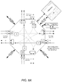
- FIG. 1 illustrates an embodiment of a HyperXTM system, including a network of processing elements (PEs) and Data Memory Routers (DMRs).
- the PEs are shown as rectangular blocks and the DMRs are shown as circles.
- the routing paths between DMRs are shown as dotted lines.
- Solid triangles show off-mesh communication and solid lines show active data communication between DMRs.
- a computational task is shown by its numerical identifier and is placed on the PE that is executing it.
- a data variable being used for communication is shown by its name and is placed on the DMR that contains it.
- the top left PE has been assigned a task with task ID 62, and may communicate with other PEs or memory via the respective DMRs adjacent to the PE, designated by communication path variables t, w, and u.
- an active communication channel connects a PE designated 71 (e.g., another task ID) to an off-mesh communication path or port via an adjacent DMR labeled "x.”
- FIG. 3 A block diagram of an embodiment of DMR hardware structure is illustrated in FIG. 3 .
- a central data memory (DM) is surrounded by an octagonal ring representing a router.
- DM central data memory
- octagonal shapes shown are merely symbolic, and that actual shapes may be different, e.g., may be rectangular.
- DMR central data memory
- PE PE-directional arrows representing data paths to other DMRs and PEs.
- These bidirectional data paths may be implemented with actual bidirectional transceivers at each end, or as a pair of unidirectional paths directed oppositely.
- Unidirectional arrows between the router and the data memory in FIG. 3 represent unidirectional data paths between memory and router.
- a small square near theses arrows represents a DMA engine, i.e., a DMA reader (DMAR) to support readout from DM, and/or a DMA writer (DMAW) to support writing data to DM.
- DMAR DMA reader
- DMAW DMA writer
- a DMAR engine generates address signals for the memory, typically to increment across a buffer, reading data to send out a link to another DMR.
- a DMAW engine generates address signals for the memory, typically to increment across a buffer, writing data that it receives from a link.
- Each DMA engine is much smaller than a PE and uses less power, so they are attractive to use for read and write of blocks of memory.
- DMA engines may be configured by PE writes to associated configuration registers in the DM memory space. Writing to a particular address triggers a DMA to start incrementing. When a DMA finishes incrementing through a block of addresses, it stops-unless configured to continue looping, either indefinitely or for a predefined number of loops.
- connections or links between ports may be short (i.e., limited to neighbors) and composed of many parallel electrically-conductive traces or "wires" or "lines".
- a link may be composed of only a few parallel traces, one trace, or a waveguide.
- the PE-to-DMR connections may separate traces for memory addresses from traces for data. Traces for data may be connected to transceivers to support bidirectional data transfer or separated into one set of traces to bring write data to memory and another set of traces to bring read data from memory.
- the DMR-to-DMR connections may not necessarily have address lines but may have lines to signify special words in the data transferred, such as control words for message header or message termination.
- All DMR connections may have additional lines for flow control, For example, a line may signal upstream (from destination to source) that further progress of data words is blocked either because there is some other communication path in the way or the destination cannot accept more data.
- this upstream line may be named “BLK”, “stall”, “rtr_busyout” or “rtr_busyin” to name a few.
- Another line may signal downstream (from source to destination) that valid data is ready. In this document this downstream line may be named “IDL”, “ready”, “rtr_rdyout”, or “rtr_rdyin”, to name a few.
- Both the upstream and downstream signaling may be used to indicate the state of transmitters and receivers connected to the ends of a link between DMRs, either local (adjacent) DMRs or global (non-adjacent) DMRs.
- communication between nodes may be under programmer control.
- communication controller 430 may direct crossbar 450 to route data from one or more of DMR input ports 404 to one or more of DMR output ports 405, and may thereby relay data along a path through a MPA.
- DMR 400 may provide additional communications paths for data.
- multi-port SRAM 425 may receive data at its write ports from either DMR input ports 401 or output registers 455 via a plurality of muxes or multiplexers. The multiplexers may allow communication controller 430 to access multi-port SRAM 425 during times when multi-port SRAM 425 might otherwise be idle.
- Router controller 430 may be programmed to select data for output from Memory Switch , any of the other three DMR In-ports 404 or a Quick Port
- a MPA embodiment may have multiple connection links between pairs of DMRs formed by space multiplexing or time multiplexing a plurality of physical connections. Pathways may be established over such connection links. However, once a pathway is established, it may not change the connection links it uses or the DMRs to which it couples during its existence.
- each pathway may be uniquely defined as an ordered sequence of DMRs and connection links, for example as a first or source DMR, a first connection link, a second DMR, a second connection link, a third DMR, a third connection link, and so forth to a last or destination DMR.
- the set of all the pathways in a MPA may be uniquely defined by the state of all the routers.
- pathways may be created quickly and destroyed quickly.
- pathway creation and destruction may be initiated by either a given PE or a given DMR.
- a given DMR may be configured to perform a DMA transfer to another DMR without PE intervention, and thus may be configured to create and destroy a pathway.
- Two methods that may accomplish dynamic pathway creation and destruction include global programming and wormhole routing. Pathway creation with global programming is described next, followed by a description of the mode and flow control features that may be common to many MPA pathways. A description of the wormhole routing method follows the mode and flow control description.
- Pathway creation or setup using the global programming method may require that every pathway in the MPA be defined by software control, and may require that each such pathway be configured before the pathway is used for data transfer. This may be done either manually by a programmer or automatically, for example by a routing compiler or auxiliary software or by selecting a library function where the function code already includes pathway setup. If an ensemble of pathways is to be used simultaneously in the MPA, then it may be up to the programmer to ensure that they do not use more communication link resources than are available in the hardware. Alternatively, software tools may be used to aid the design of link resource usage.
- the communication controllers such as communication controller 430 of FIG. 4
- the instructions may load the appropriate crossbar configuration register 451 bit-groups associated with each link in the path.
- the instructions may do this immediately or in a sequence, while in other embodiments they may await a trigger signal of some sort.
- the hardware may or may not prevent pathways from being interrupted once established. Therefore, it may be the responsibility of the programmer or routing software to ensure only one pathway is assigned to any given link at a time. Once the Router Control state registers 451 in the DMRs all along the pathway are set, the communication pathway may be complete and ready for data.
- a pathway may be destroyed when it is no longer required by altering the related bit-group in the crossbar configuration registers of every DMR included in the pathway.
- an existing pathway may be left intact indefinitely, and the Router Control states along a pathway may simply be overwritten by new pathways as needed after the existing pathway is no longer required.
- some MPA embodiments may provide some additional circuits. These may include, for each DMR-type port, an additional control line indicating control/data status and denoted C/D, which may be included in every connection link between DMRs and coupled to routing logic 435 in each DMR.
- the maximum number of wires in the connection link may nominally correspond to the sum of the number of bits per data word, plus one wire each for C/D, IDL, and BLK, the latter two for flow control, defined above.
- these signals may be multiplexed in a number of different ways to reduce total wire count.
- the C/D bit may be used by the receiving DMR to distinguish header, body, and tail words of a worm. If the C/D bit is de-asserted, it may indicate that the received word is a body word. A body word may correspond to a data word plus the control bit, which may be passed along the pathway unchanged. If the C/D bit is asserted, it may indicate that the received word is a control word. A control word may allow the data portion of the word to contain a routing code for interpretation by routing logic 435.
- One important feature of the routing code may be an indication of whether the control word is a header or a tail; thus, an H/T bit indicating header/tail status of a control word may be provided.
- the H/T bit may be adjacent to the C/D bit, but in other embodiments it may be assigned to other bit positions or may be a specific multibit code. If the control word is a tail word, then it may be propagated along the pathway and may sequentially free DMR output ports for use by some other pathway.
- a control word is a header word it may be latched within input register 454 of the receiving DMR and decoded by combinatorial logic in routing logic 435. Routing logic 435 may examine the appropriate bits of the header word as well as the port from which the header came, and may issue a request of crossbar 450 for an output port as shown in Table 1. The several bits examined by routing logic 435 for the purpose of requesting an output port may be referred to as a navigation unit, or NUNIT. For a DMR embodiment that includes four DMR-type output ports per DMR, a NUNIT may use a two-bit code to specify the four direction options, as shown in Table 1. In other embodiments that include the same or different numbers of DMR-type ports, other NUNIT codes may be used.
- routing logic 435 may evaluate the NUNIT and allow the worm to proceed. For example, if a header word arrived from SRAM (a type of DM) with a NUNIT code of 10, routing logic 435 may request the East output port from crossbar 450 for the header word and subsequent words of this worm. Table 1. Output port as a function of direction code and input port. Input ports Direction (code) North East South West SRAM Straight through (11) S W N E N Left turn (10) E S W N E W turn (01) W N E S S Null (00) SRAM SRAM SRAM SRAM SRAM SRAM W
- FIG. 17 illustrates operation of one embodiment of routing logic on a header word.
- FIG. 17 depicts a header word as it progresses through multiple DMR nodes on a pathway from a source node to a destination node.
- Case (a) may illustrate a header word in its initial state originating in a source DMR. In this state, the header word includes a C/D bit, an H/T bit, and a plurality of header NUNIT fields numbered HN0 through HN4, with HN0 occupying the least significant bits of the header word.
- the header word may be passed on to the output of the crossbar with modification as follows.
- the header word may be right shifted by one NUNIT and filled with zeroes from the left.
- the C/D and H/T bits may then be restored to their original positions.
- Cases (b) through (e) of FIG. 10 may illustrate the header modification that occurs after the header has been processed by one through four DMRs, respectively.
- the lead header word may fill with more zeroes until the null code is in the rightmost NUNIT, as shown in case (e). If the null code is the rightmost NUNIT when the header word is not from the same DMR (controller or neighbor DMR), and the next worm word is not a control word, then the header word may be at the destination DMR for that worm.
- the check for arrival at the destination DMR may require multiple clocks.
- First the lead header word may be moved into one of input registers 454 and tested by the Router Control logic 435 for the null code in the rightmost NUNIT. If the null code is found, then in the next clock cycle the next word of the worm may overwrite the lead header word and its C/D and H/T bits may be tested. If the next word is another header word then it may become the new lead header word, and its rightmost NUNIT may be used to select the output port for the next DMR. There may be many header words per worm in order to route across large arrays. If the next word is a body word rather than a header word, the worm may be at its destination DMR.
- the body word may be written to a preset SRAM location in the DMR.
- the arrival of a body word at a location may be detected by the DMA logic of communication controller 430, or by a DMR, either of which may service the arrival of subsequent body words.
- Information regarding how to service the worm may either be preloaded at the destination node or included in the worm right after the header.
- FIG. 18 is a block diagram illustrating an example pathway through a portion of a MPA.
- FIG. 18 depicts eight routers denoted “Router A" through “Router H.” Each depicted router may be exemplary of router of FIG. 4B .
- each depicted crossbar may be included in a respective DMR such as, e.g., DMR 400 as illustrated in FIG. 4 , and each such DMR may be coupled to other DMRs within a MPA, such as MPA 20 as illustrated in FIG. 2 , for example.
- each of routers A-H includes four input ports denoted N, S, E, and W on the left edge of the router as well as four output ports denoted N, S, E, and W on the right edge of the router.
- Each route's input ports may be coupled to DMR input ports 404 of the respective DMR, and each router's output ports may be coupled to DMR output ports 405 of the respective DMR.
- each of routers A-H includes an input connection and an output connection to a memory, such as multi-port SRAM 425 of FIG. 4 , which connection is denoted M on the left and right edges of the router, respectively.
- each router A-H is coupled to a plurality of neighboring routers via each respective DMR such that each output port N, S, E, W of each router is coupled to a respective input port S, N, W, E of each of the plurality of neighboring routers.
- each router may be coupled to receive inputs from and send outputs to four neighboring routers. It is noted that in alternative embodiments, different number of routers, each including a different number of input ports, output ports, and memory connections, may be employed.
- FIG. 18 illustrates a pathway from a source DMR including router A to a destination DMR including router H, which pathway traverses DMRs including routers B, F, and G.
- a 2-bit NUNIT code defined according to Table 1 may be used to implement the illustrated pathway as follows.
- the pathway originates in the SRAM coupled to router A via input memory connection M and exits router A via output port E.
- the NUNIT for router A should be 10.
- Output E of router A is coupled to input W of router B, and the illustrated pathway exits router B via output port S.
- the NUNIT for router B should be 01.
- Output S of router B is coupled to input N of router F, and the illustrated pathway exits router F via output port E.
- the NUNIT for router F should be 10.
- Output E of router F is coupled to input W of router G, and the illustrated pathway exits router G via output port E.
- the NUNIT for router G should be 11.
- output E of router G is coupled to input W of router H, and the illustrated pathway ends in the SRAM coupled to router H via output memory connection M.
- the NUNIT for crossbar H should be 00.
- a header control-word implementing a wormhole routing in the format of FIG. 17 for the path illustrated in FIG. 18 may include an asserted C/D bit indicating a control word, an asserted H/T bit indicating a header word, and the values 00,11, 10, 01, and 10 corresponding to fields HN4 through HN0, respectively.
- the illustrated pathway is merely one of many possible pathways through one MPA embodiment. In other embodiments, different numbers of routers and ports may be employed, and different pathways and routing methods are possible and contemplated.
- each NUNIT may be consumed by a specific DMR along a pathway, one or more bits may be added to each NUNIT to request specific behavior at individual DMRs. For example, in one embodiment, one added bit per NUNIT may be used to specify that a given DMR shall operate in a multi-layer mode or not. In such an embodiment, a wormhole-routed path may use different modes at different DMRs along the way depending on the programming of the header.
- a PE may send a header word directly to the crossbar inputs of a neighboring DMR, such as DMR 400 as illustrated in FIG. 4 , for example.
- a PE may do so by specifying a particular Register address to a neighboring DMR via DMR address ports, and sending the header word(s) to the output Router of that DMR via same Register address.
- Routing Control logic such as, e.g., routing control logic 435 as depicted in FIG. 4 , may be configured to then send the worm on its way to its destination without using the Memory Switch or Memory. This technique may provide a more efficient short message passing capability between PEs.
- a pathway being set up by wormhole routing may come upon a DMR with one or more other pathways either already routed or in the process of being routed through a given DMR.
- a resource conflict may occur when one or more inbound header words requests the same crossbar output port at the same time (a collision) or when the output port is already occupied by a pathway (a blockage).
- Routing Control logic may include logic configured to arbitrate which pathway receives access to the contested output port in case of a collision. Routing Control logic may detect the collision and grant only one worm access to the contested output port.
- Various priority/rotation schemes e.g., a round-robin scheme
- worm is used here to represent an ordered sequence, or string, of flow units (referred to as “flits” in the literature) that may be words, bytes, or other bit groups.
- the DMR flow control protocol may operate as follows. When a worm encounters a blockage, the lead flit of the worm may be latched in an input register of the blocking DMR, and the BLK signal may be driven backward to the next upstream DMR in the pathway to latch another flit of the worm in input registers of the next upstream DMR.
- This process may be repeated back to the DMR containing the tail word of the worm, or to the source DMR if the tail word has not yet been sent by the source.
- the data in the worm may be captured in the input registers and output registers of DMRs in the pathway that are configured to operate in a synchronous data transfer mode.
- two words may be stored per DMR, resulting in a "scrunched” or "telescoped” condition of the stalled worm.
- the worm may stay frozen indefinitely until the blocking conditions go away, following which, its forward motion may be automatically restarted by the propagation of the de-assertion of the BLK signal.
- DMR flow control protocols assumes one flit to be stored in a link input port register and one flit to be stored in a link output port register; however, additional registers may be added to store additional flits per port under blockage conditions, and this may provide additional elasticity to the length of the worm.
- the source end of a particular pathway may stop sending flits temporarily and de-assert the "ready" signal, and the flow control signaling may progressively stop the forward motion of flits until the destination end receives the de-assertion of the "ready" signal, whereupon the worm will be frozen in place until the source starts sending again.
- the temporary stop of source data sending and de-assertion of the "ready" signal may create a bubble in the pathway composed of flits with a de-asserted "ready” bit.
- the bubble may progressively grow until either the source resumes sending data or the bubble reaches the destination, whereupon the destination receiver continues to read flits but discards all flits which contain de-asserted ready bit.
- the source resumes sending data the bubble collapses against the destination receiver; and the destination receiver may resume receiving data upon the appearance of an asserted "ready” bit.
- multiple protocols may be supported by hardware and selected by software.
- Multi-processor systems such as those described above, may require hardware (e.g., DMRs and PEs) and software to work in a cooperative manner in order to accomplish a particular computing task.
- a network may be used to transmit data and instructions between individual processors.
- multiple networks may be employed for communication between processors.
- a network within a multi-processor system that has high data throughput capacity may be designated as a primary interconnect network (PIN), which may be composed of links (i.e., one or more wires that run between nodes) and nodes. Nodes may have ports that may be employed to connect to local processing engines, local memory units, or to I/O ports at the boundary of the multi-processor array.
- PIN primary interconnect network
- Other networks which may be constructed in a similar fashion, with lower data throughput capacity, may be designated as secondary interconnection networks (SINs), such as, e.g., the serial network described in U.S. Patent Application 13/274,138 . Such secondary networks may be used for control, testing, debug, security, and any other suitable application.
- Nodes may include a switch, which may be capable of making independent connections between one link or port and another link or port, and may correspond to a DMR.
- nodes located near the edge of an integrated circuit may have specialized ports for off-chip communication with other IC chips of the same or different types, such as, random access memories (RAMs) or general purpose processors (GPPs), for example.
- RAMs random access memories
- GPPs general purpose processors
- a PIN topology may include a 2-dimensional mesh consisting of a 2-dimensional array of nodes. Each node may have a north, south, east, and west link to another node.
- a 3-dimensional mesh may be achieved with the addition of adding "up” and “down” links to each node of a 2-dimensional mesh allowing the connection of one or more 2-dimensional meshes. 3-dimensional meshes may be connected in a similar fashion to form what is commonly known as a "hypercube mesh.”
- 2-dimensional and 3-dimensional meshes have been described, in other embodiments, any suitable number of dimensions may be employed to form a multi-dimensional mesh. A dimension need not be infinite in potential extent; instead it may loop back on itself, forming a mesh cylinder or a mesh torus.
- a group of PE may be interconnected with a PIN which is randomly formed and then mapped so as to give addresses to destinations
- Wiring technology may influence the relative density of links in each dimension.
- available wiring density is high in the circuit plane, but limited in the third dimension.
- a 3-dimensional mesh may be accommodated by using less links in the third dimension, or by projecting all of the links into the circuit plane. Nodes and link routing may then be adjusted to create an area-efficient layout.
- Such a layered approach to forming networks may allow for high dimension networks without the need for exotic fabrication technology.
- Higher dimension interconnection networks may provide more communication pathways between computation resources, i.e., processing engines and memory units.
- links may be routed across memory units, allowing additional PIN resources with minimal increase to silicon area of a multi-processor system.
- Higher dimension networks may also be implemented using advanced packaging techniques including through-silicon vias (TSV) and various types of silicon interposer technologies.
- TSV through-silicon vias
- a node may include a data-path switch, flow-control signaling, and a router control mechanism (RCM).
- the data-path switch may be configured to establish connections, each connection enabling a data path between an allowed subset of links and ports. For example, a connection may be established between a link and a different link, between a link and a port, or between a port and a different port.
- the data-path switch may include word-wide bit-parallel multiplexer whose outputs may be coupled to the outgoing portion of a link or port, and their inputs may be coupled to the incoming portion of a link or port.
- synchronously clocked registers may be used at a link or port interface to buffer incoming or outgoing data and adjust its timing.
- the data path switch may be implemented with a single stage of multiplexing, while in other embodiments, the data path switch may be implemented with multiple stages of multiplexing.
- the multi-layer IN switching node of one embodiment of the invention in its most general form, includes layer switching and directional switching for multiple communication pathways that may be sourced at the node, traversing the node, or terminating at the node.
- the node interprets the inbound data arriving at its ports according to a configurable protocol to determine what to do with it.
- the smallest unit of data that can be accepted by the ports that are linked to other nodes in the IN is also the smallest unit subject to data flow control on the links, and in the literature it is referred to as a flow unit or "flit.”
- the flow control signaling may regulate the flow of data across each connection so that data is not lost by a sending more data than a receiver can absorb, or by a receiver duplicating data that a sender could not send fast enough.
- Data sent into a channel at a source port may appear at its destination port after some period of latency. In some cases, the latency period may correspond to one clock period per link traversed.
- the rate of data flow in the channel may be controlled by hardware, software, or a combination thereof.
- hardware flow control signaling may use a binary electrical signal from sender to receiver indicating that data is ready, and another binary electrical signal from receiver to sender requesting that the sender should wait (stall) before sending more data. These flow control signals may follow a data path in parallel, including transit through data multiplexers.
- the route control mechanism may be configured to process connection requests for resources (links or ports).
- an RCM may search across multiple inputs (generally from different directions) for an incoming signal. If the signal contains a code requesting a particular resource, the RCM may check that the requested resources are available, i.e., the resources are not reserved by a pre-existing connection. If requested resources are available, an RCM may grant the request, send a signal to data path multiplexers to make the connection, and establish flow control signaling across the connection. Conversely, if requested resources are not available, the RCM may not grant the request and may signal the requesting input to stall the sender until the incompatible pre-existing conditions are removed.
- the RCM may time-share the blocking connection and allow the requested connection on a part-time basis (commonly referred to as "cut-through"). While stalling or time-sharing any particular subset of the inputs, the RCM may search the remaining set of inputs for an incoming signal.
- An RCM may include an arbitration mechanism to deal with simultaneous requests for available resources. If two or more connection requests for the same resource (link or port) arrive at the same time, an RCM may arbitrate them and select a winner.
- the arbitration scheme may be a priority scheme, a round-robin scheme, or any other suitable arbitration method. In other embodiments, the arbitration scheme may be configurable to be a priority scheme, round-robin, or any other suitable arbitration method.
- an RCM may relay the termination command to any output link, and release the resources associated with the connection. Released resources may be immediately available for making other connections. In cases where a cut-through had been established, the RCM may restore the resources to the pre-existing connection that was cut. It is noted that in various embodiments, an RCM may perform other functions or duties.
- Routing through a PIN may be performed in a hierarchical fashion, with different techniques employed at different levels of the hierarchy.
- the RCM within a node is the lowest level, the setup and tear down of communication pathways (channels) is the intermediate level, and the group selection of pathways to minimize mutual interference is the top level.
- routing is basic and fast, and typically is implemented in hardware.
- the routing is more complicated and may be accomplished in software.
- routing is accomplished with the routing control mechanism as described in more detail above.
- the RCM may be implemented as a state machine. Routing request may arrive from a local PE via a port into the node. Routing requests may also arrive from a link, encoded in a header of a message. As described above in more detail, routing requests encoded in a message form the basis of a channel configuration method commonly referred to as "wormhole routing." In such a routing method, a message is composed at a source node and prefixed with a header that describes where a channel is to go. In various embodiments, different header styles may be employed.
- An RCM may also monitor the traffic in connected channels and use this information to locally adjust connections into more optimal arrangements. For example, if two paths are time shared on a link and one of the paths is relatively busy compared to the other connection, the RCM may be permitted to allocate a larger fraction of time to the path with higher traffic load. In another example, if a switch node has additional links to bypass local traffic, then through traffic may be shifted to these links, freeing up local resources for sourcing or terminating a path.
- a "tail" code may be sent into the source port of the path.
- the tail code may sent automatically by the hardware of the system.
- Software may control the sending of the tail code in other embodiments.
- individual RCMs clear the connections and release its respective routing resources.
- the tail code insertion can be automatic via hardware or sent under software control.
- extra data bits may be included in the links to distinguish header and tail words from the message body.
- a word parity bit may also be carried in any link to assist in data integrity.
- Pathways may be static or dynamic.
- a static path may be set up and used for the duration of a given application, while a dynamic path may be created for message transfer and then torn down, freeing links and nodes for other pathways to be formed.
- a dynamic path may be torn down and replaced at a later time by another instance of itself.
- a worm header may contain routing information such as source address, intermediate addresses, destination address, and mode requests.
- the destination address is usually required and it may be coded in many different ways.
- an address may be encoded as a sequence of turns while, in other embodiments, an address may be encoded as Cartersian X-Y pairs, or any other suitable encoding method.
- the routing information may take the form of a sequence of navigation units (commonly referred to as "nunits"). The nunits may be encoded to request connection resources (links or ports) and modes of each node and RCM that is encountered while setting up a communication pathway.
- Minimal (2-bit) nunit codes may request to connect "straight-ahead,” “turn left,” “turn right,” or “stop.” As a header message passes through a node, the sequence of nunits may be shortened from the front as the connection instructions are executed.
- the RCM may direct the data path multiplexers to present the remainder of the worm message to a register for access by a PE or DMA. Multiple such registers may be supported in a DMR so as to support multiple channels simultaneously. The address of such a register may map to the corresponding arrival direction at the destination node, enabling a particular PE to wait for the arrival of a message from a particular direction.
- any suitable number of bits may be used in navigation to allow for INs with higher dimension mesh connections and also for additional router modes.
- an additional bit may be encoded in each nunit.
- An additional nunit bit may allow for connection instructions to switch layers, "go up,” or “go down,” and may be compatible with a two or more layer PIN.
- An additional nunit bit might be used to modify router modes, such as fixed or optimizing, where optimizing might apply to time-share ration, express routing using non-nearest neighbor links, or other optimizations.
- Application software on a multi-processor array may require an ensemble of many communication pathways between and among PE and chip I/O interfaces. Since two or more pathways may block each other, and the probability of blocking becomes a certainty when too many paths are crowded onto finite resources, the routing of an ensemble of pathways reduces to finding at least one feasible (non-interfering) ensemble of routes. As the density of paths increases, a feasible ensemble may become more difficult to find.
- a measure of path density is the path-to-link fill ratio (i.e., the total length of paths divided by the total length of links). As the fill ratio approaches 100% it may become impossible to complete all of the path routes.
- Routing of an ensemble of communication pathways may be accomplished with a software tool referred to as a "router" which may be included as part of the development suite of software.
- a programmer (perhaps employing a task placement tool) may provide the router tool with a list of paths that need to be routed, also referred to as a netlist. Initially, a path may only be specified by the location of its source and destination nodes. For each path to be routed, the router may select a minimum-distance sequence of links from the source to the destination. When after the first pass, there are paths blocking other paths, the ensemble may be re-routed using blockage reduction techniques. The re-routing with blockage reduction may be repeated until no blockages are detected.
- a method to make the routing process easier may involve restructuring the application software algorithm to reduce the number of paths required.
- path density is high when multiple paths are seeking the same node or attempting to exit from a node.
- an algorithm may be distributed across multiple nodes, effectively distributing message traffic across more links.
- the DMR link capacity may be increased to allow more connections per node.
- Another method to make the routing process easier may involve increasing the number of available connection resources (links and switches) per DMR.
- the additional resources may be organized in layers added to the IN.
- Each added layer may contain a set of node to node connections, and each router may include a set of data path multiplexers, flow control signaling, and a router control mechanism. To permit any communication pathway to cross from one layer to another, additional data path switches and their control may be needed.
- FIG. 5A shows an example embodiment of a single layer directional switch for a DMR node 550 in a single layer IN.
- Links between DMR nodes connect to input and output ports on each DMR. These ports in turn connect to a directional switch (router) in the DMR.
- the Router input components 552, 554, 556, and 558 are further detailed in the lower half of FIG 4B - items 482, and 486.
- the Router output components 551, 553, 555, and 557 are further detailed in the upper half of FIG 4B - items 481, 485, 487, and Router Control Logic 489.
- the Input port data register 486 buffers input flits and connects to three Router output components (for turn left, go straight, or turn right) and (for terminating pathways) to the Memory Switch 488, and the Quick Ports (not shown) to be available directly to be connected PEs.
- the lines drawn between Router input components and Router output components represent multi-bit busses that may be selected by Router Control Logic 489 and data-path multiplexers 485 in the output components.
- FIG. 5B illustrates an embodiment of a two-layer directional switch for a DMR node 500 in a two-layer IN.
- node 500 includes an added global (layer B) composed of output ports 501, 505, 509, and 513, and the B side of the input switches.
- layer B the lines drawn between B-side of input switches and Goports represent connections of multi-bit busses that may be selected by data-path multiplexers at the Goports.
- the pre-existing local (layer A) directional switch may be the same as shown in FIGs 4B and 5A ; but to keep FIG 5B uncluttered, only the output ports 502, 506, 510, and 514, and inputs ports 503, 508, 512, and 515 of Layer A are shown.
- Node 500 further includes input switches 504, 507, 511, and 516 that are coupled to the local (layer A) inputs ports 503, 508, 512, and 515, respectively.
- the purpose of the input switches is to allow an inbound communication pathway to switch from the local (layer A) to the global (layer B) or from the global (layer B) to the local (layer A).
- crossbar switches 504, 507, 511, and 516 may be composed of 2 input and 2 output (2X2) crossbar switches capable of only two states, one being straight-through connections and the other being crossed connections.
- the input switch control logic (not shown) may be separated from the router control logic 489. Taken together the input switch control logic and the router control logic may be considered the router control mechanism.
- Each crossbar switch receives data from an A port and a B port and selectively passes data either through on the same layers or crossed from layer to layer.
- Local (layer A) output ports 502, 506, 510, and 514 may accept data from DMA or PE and transmit data to their respective A links.
- the local (layer A) output ports may also connect with input ports 503, 508, 512, and 515 to allow for the creation of through routes.
- Global output ports 501, 505, 509, and 513 may accept data from B side of crossbar switches 504, 507, 511, and 516 and transmit data on their respective B links
- the global output ports may not be used in conjunction with local routes.
- port configuration of the node illustrated in FIG. 5B is merely an example. In other embodiments, different numbers, and configurations, and interconnections of ports may be possible.
- FIG. 6 An embodiment of a portion of a multi-processor array is illustrated in FIG. 6 .
- the illustrated embodiment includes DMR 601 coupled to DMR 602 through local link 611 and global link 610.
- DMR 601 is further coupled to PE 603, and DMR 602 is also further coupled to DMR 602.
- DMR 601 global link 610 and local link 611 are coupled to crossbar switch 604, which is further coupled to global port 605 and local port 606.
- DMR 602 global link 610 and local link 611 are coupled to crossbar switch 607, which is further coupled to global port 608 and local port 609.
- data transmitted from local port 606 of DMR 601 may be coupled to local link 611.
- the crossbars are only on the input port side.
- data transmitted from global port 605 may be coupled to local link 611 or to global link 610 by crossbar switch 604. Again, data from global port 605 can only go out on global link 610.
- data received by DMR 602 via global link 610 may be routed to either local port 608 or global port 609 through crossbar switch 607.
- crossbar switch 604 only has two active states of straight or crossed. For example, when global link 610 is connected to local port 608 then local link 611 can only be connected to global port 609, and when global link 610 is connected to global port 609 then local link 611 can only be connected to local port 608.
- node-to-node link in an IN of a multi-processor array illustrated in FIG. 6 is merely an example. In other embodiments, different numbers and types of connections between DMRs are possible and contemplated, including bidirectional and time shared connections.
- DMR 700 includes local ports 701, 703, 705, and 707, and global ports 702, 704, 706, and 708.
- DMR 700 further includes local memory 709.
- local port 701 is coupled to local ports 703, 705, and 707.
- Local port 701 is further coupled to local memory 708.
- the aforementioned coupling may be set up by an RCM as described in more detail above, and the coupling may allow through-routes in DMR 700.
- data transmitted from a neighboring DMR to local port 701 may be passed through the output portion of any of local ports 703, 705, and 707.
- data received through local port 701 may be stored in local memory 709.
- the number of ports and their arrangement and internal routing illustrated in FIG. 7 is merely an example. In various embodiments, different number of ports and different configurations of internal routing may be employed.
- DMR 800 includes local ports 801, 803, 805, and 807, and global ports 802, 804, 806, and 808.
- global port 802 is coupled to global ports 804, 806, and 808.
- the aforementioned coupling may be setup by an RCM as described in more detail above, and the coupling may allow through-routes in DMR 802. For example, data transmitted from a neighboring DMR to global port 802 may be passed through the output portion of any of global ports 804, 806, and 808.
- FIG. 8 The arrangement of ports illustrated in FIG. 8 is merely an example. In other embodiments, different numbers of ports and different arrangements of ports are possible and contemplated.
- the input switch control logic may have configurable priorities.
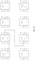
- a table depicting example input switch control priorities is illustrated in FIG. 9 .
- input router port A For incoming pathway routes that are programmed to remain on local (layer A), input router port A may have a higher priority than input router port B.
- input router port B In the case of incoming global (layer B) routes, input router port B may have a higher priority than input router port A.
- the higher priority port may control the input switch state and thereby the access to the resource, and the lower priority port may follow if the requested resource is available, or it may stall if the resource is unavailable.
- priorities are depicted in the table illustrated in FIG. 9 .
- the routing table of Fig 9 corresponds to a semi-automatic mode of the example routing protocol that allows the layer switch control logic hardware to make layer switching selections during pathway setup based on the current state of the node and the directional switching requests presented to it.
- This mode is advantageous to processing flits that contain minimal sized nunits that only specify direction requests, and in some cases it may avoid blockages from other pathways.
- the non-automatic mode of the example routing protocol may not allow the control logic hardware any freedom to make selections of data path switches (layers or directions), and instead require the selection to be encoded in the current nunit of the arriving header flit.
- This mode may require larger nunits than the semi-automatic mode, and these may be accommodated with proportionately more header flits to set up a wormhole routed communication pathway.
- This mode is advantageous to the precise control of pathway location by a software development tool suite, which has a much wider view of the ensemble of paths needed by an application software, and is better equipped to avoid blockages and infeasible ensembles of pathways than would be obtained with path selection blind to other pathways.
- configurable control logic for the layer and direction switches supports multi-mode routing protocols.
- the current configuration is held by a register in the DMR that is R/W accessible to application software.
- Each DMR may be configured independently of the other DMR, so it is possible that a header flit to set up a worm-routed pathway will have nunits of mixed sizes, depending on the expected mode setting of the DMRs that it is intended to encounter.
- the crossbar switch may implement all cases of inbound pathway setup, except the case when both ports (A and B) request a local (layer A) access. When both ports request a local access, the crossbar switch may stall input router port B. In some embodiments, the crossbar switch may allow access, but downstream fabric priority logic may stall the request. In order to minimize the impact on timing, the crossbar switch may be designed to switch to the proper state based on minimum logic that uses only the current header flit requests and crossbar state. No additional downstream stalling is considered. This may give rise to cases where a potentially bad decision may be made based on the limited look at the state.
- the input crossbar is not currently “locked” on an existing active transaction.
- a global request is made by an arriving first header flit on either the A and/or B port.
- the first header flit may be placed on the B' (global) bus and sent to the Goport logic.
- This Goport logic is either already in use by another pathway (from a different direction) or is receiving a second header flit request in the same cycle from a direction with a higher priority.
- the first header flit will be stalled downstream from the input crossbar and so it will have to wait for the Goport to become available.
- the Outport (layer A) associated with the requested route direction is available for a global route but the logic would be too complex to execute in a single cycle to detect that.
- a "stall and retry" tactic may be employed.
- the request may be stalled; and the during the same complete clock cycle all the necessary logic may be evaluated to determine if a different decision by the layer switch input crossbar will provide a clear path. If that is the case, then the relevant information may be registered at the next rising clock edge and a retry may be evaluated in conjunction with any new requests. When no new requests (on the same or other ports) conflict with the retry, then the retry may be granted and the route may be completed on the alternate path.
- the aforementioned method provides full use of the global route fabric as if all of the conditions were considered in the first request cycle without over-taxing a cycle's logic in such a way as to cause a critical speed path.
- the route set-up is still deterministic, based on the current conditions in the fabric, but a route may take additional cycles to traverse a DMR when a retry is necessary.
- the crossbar may be controlled by hardware or software (such as, e.g., nunit/flit programming and control registers), or a combination thereof.
- PE 1006 creates a worm header to route from an east port of DMR 1001 to a west port of DMR 1003.
- the route originates from router port A or DMR 1001 and then travels to DMR 1002.
- the layer-switch input crossbar in DMR 1002 decides to send the worm onward using router port B (a global port) onto DMR 1003.
- the layer switch in DMR 1003 switches the route back to the local (layer A) input port, allowing the wormhole path to terminate there.
- This route originates from router port A (north) of DMR 1005.
- the route switches to router port B (east) of DMR 1001.
- the route switches to router port A (west) of DMR 1002 due to the fixed state of the input crossbar switch (e.g., the crossbar switch is already set in a direction by the route established by PE 1006 as described above).
- the route switches back to the global routing level (level B) at DMR 1003.
- the route exits DMR 1003 and enters DMR 1004 via router port B and then is switched to the local input route port where the wormhole routing terminates.
- routes depicted in FIG. 10 are merely examples. In other embodiments, different numbers of routes and different routes paths are possible.
- Areas of an MPA chip may need to be secured from other areas of an MPA chip. For various reasons, one area of an MPA may contain sensitive data related to device control, IP licensing, user authorization, etc., or running an algorithm critical to proper operation. Meanwhile another area of the MPA may be executing software that has not been validated as secure. Non-validated software may be present for a variety of reasons (it may be new and with plenty of bugs, or the source code is unavailable for security validation, or it may be so large and complex that it is un-economic to validate). Non-validated software may contain viruses or spyware.
- a wormhole-routed communication path may be designed to be sourced in one area, to probe another area, and to copy-in or copy-out data or instructions.
- the links and ports of a DMR may be designed such that they may be configurably disabled, see U.S. Patent Application Serial No. 13/274,138 , referenced above.
- the DMR links and ports involved are shown in Fig 8A wherein circular features are points where message traffic can be disabled.
- a configuration register in the SBS interface to the serial bus that may be designed so that individual bits may be written to disable each of the DMR ports/links.
- the serial bus may be a low-bandwidth secondary interconnection network (SIN) on the chip that may be used for configuration and debug purposes.
- SI low-bandwidth secondary interconnection network
- Figure 23 shows an MPA with an area delineated by a freehand boundary that may be secured by disabling communication pathways at the boundary. Communication paths within the secured area are not affected by the disabled communications at the boundary. However, the bounded area is large enough that it gets in the way of communications between PE on either side of the secured area. Thus there is a need for a way to route unsecured messages across the secure area without violating its security (referred to herein as "Secure Bypass Routing").
- Secure Bypass Routing may be achieved by designing a DMR to be able to configurably limit worm-messages from connecting to the local memory and PE ports, but to allow bypass over secured areas.
- a DMR may be designed such that memory and PE ports connect directly to only the local layer-A data paths, and not to other layer data paths, except indirectly through the layer switches (input crossbars).
- the worm-message layer switching is limited to the input crossbars, and a way to prevent a worm-message from switching layers in a DMR is to lock the crossbars into the straight-through state.
- the crossbars For a two-layer IN the crossbars have only two states (through or crossed). When these crossbars are locked in the through state, then any inbound worm-message is constrained to exit the crossbar on the same layer. In the embodiment illustrated in FIG. 5A , worm-messages inbound on the local layer-A may exit on the layer-A OUTPORT or they may terminate at the INPORT. Worm-messages inbound on the global layer-B may only exit on the layer-B GOPORT.
- the crossbars may have many states and may include the connection of any input layer to the local layer-A. If these "connect to local INPORT" states are the ones locked off, then inbound worm messages on upper layers may switch layers but be excluded from INPORT, thus keeping INPORT secure. In some situations it may be desirable to allow some of the upper layer inbound communication pathways to reach the DMR INPORTs, and this can be accommodated with more programming bits in the DMR configuration register.
- FIG. 19 An unsecured communication pathway over a secure region is illustrated in FIG. 19 where the dotted line depict a route that passes on the global (layer B) links over a secured area; and it does not originate or terminate within the secured area.
- config-reg is an abbreviation for configuration register:
- PE(1,0) using a Quick port in DMR(2,0) may write header flits to the DMR(2,0) South Quick Port that arrive at DMR(1,1) on the A layer and then are switched to the B' layer.
- the bypass route may continue on the link to DMR(1,1) on the B layer.
- the bypass route may go North, South, or East according to the nunit information in the header flits.
- a nunit selects South then the bypass route would continue on to DMR(0,1) where it may continue on the B layer or, now that it is outside the secure area, it may switch to the A layer and continue to route or terminate.
- control logic and the data-path switching to implement a protocol in the example HyperX DMR nodes are implemented in two stages - first the layer-switching crossbar, and then the directional-switching router. Alternatively in other implementations the directional switching could come first and the layer switching second. These two stages may be integrated together into a unified switch in other implementations. Alternatively the protocol and switching may be implemented with more than two stages.
- the example DMR router implementation has a layer-switch (input crossbar) that is a two-layer version of a multi-layer switch, while the example directional switch is a three-direction version of a multi-directional switch.
- This embodiment does not limit either of these switch components to the number of layers and directions of this example DMR implementation.
- the concept may easily be extended to many layers and many directions with minor modifications to the example implementation. These extended forms support additional IN connection dimensionality.
- the wormhole routing methods described here and used in the example HyperX architecture provide for an infinite address space by using continuation header flits. For short distance communications a single header flit may be all that is required. When the DMR encounters a first header flit with only one non-termination nunit, then the DMR may perform the nunit specified direction selection, discard the first flit, promote the second flit to first flit and send the worm message onward to the next DMR. Very long headers may be composed if required to traverse an MPA spread across many f MPA chips. Finite addressing of worm message headers uses a fixed number of bits to specify the worm's destination address. Finite addressing does not interfere with the multilayer methods described here for low dimensional INs, but it may become less efficient as the IN dimensionality increases.
- the routing engine may use information about the route congestion both locally and more globally to allow it to detour a route around pockets of congestion.
- a pathway route may be planned and programmed into header flits as usual, and then if congestion is encountered along the way, an unplanned detour may be made to avoid it.
- the routing control mechanism of an IN node may compute a detour either alone or in conjunction with information from neighboring nodes, either local or global.
- a node may add nunits or header flits as required to achieve the detour, after which the worm-message may continue on its pre-planned route to its destination. If temporal knowledge is also included in the route information then the estimated duration of congestion can also be used as part of the determination of the path. Overall this is a congestion avoidance adaptation on the fixed path methods previously described.
- Congestion may be determined according to the method illustrated by the block diagram in FIG 26.
- the square boxes represent DMRs.
- the DMR in the center labeled "A”
- the surrounding DMRs (B1-B8) may provide metrics on both local and global congestion information to DMR A.
- a single metric from DMR B1 to DMR A tells DMR A about the level of congestion DMR B1 is observing itself. This is the local congestion metric.
- DMR B1 also provides a global congestion metric to DMR A by gathering information from its neighboring DMRs that are not neighbors of DMR A. These have been marked "C" in FIG 26.
- DMR B2 provides a local congestion metric to DMR A. It also provides a global congestion metric to DMR A by gathering information from its neighboring DMRs that are not neighbors of DMR A. These have been marked “D” in FIG 26. This repeats for all of the neighbors of DMR A as indicated in FIG 26. Note that this method of determining congestion can be expanded in multiple dimensions and can use information from further away neighbors to determine global congestion as required by the topology of the PIN and the needs of the algorithm calculating the automatic detour routing.
- TDM time division multiplexing
- Multi-processor arrays such as those described above, may be used to process high-speed data streams with complex algorithms. Such data streams are often continuous and arrive and depart at a constant rate.
- the PEs are better suited to processing data in memory in a block-at-a-time fashion; so there is a mismatch to the continuous data streams.
- One solution to this problem is to allocate a portion of memory for use as a buffer memory, also referred to as a buffer.
- a buffer is specified in application software that is compiled to operate the MPA.
- a buffer may be allocated statically at compile time or dynamically during operation.
- array is not meant to imply any dimensionality.
- a memory buffer may provide an elastic quality to a data path within a multi-processor array.
- a buffer may be able to absorb short-term data rate variations (provided that average input and output data rates are matched).
- it may be necessary to split a high rate data stream into multiple low rate data streams.
- it may be necessary, in other applications to combine multiple low rate data streams into a single high rate data stream.
- Such operations may require that there is no loss or duplication of data within any of the data streams.
- a PE may be used to store data into the portion of a memory allocated for a memory buffer. The same PE or another PE may be used to retrieve data from the buffer. Such a method of data storage and retrieval, however, underutilizes the capabilities of a PE.
- a simpler direct memory access (DMA) engine may, in some embodiments, be used to access buffers and move data, thereby freeing the PE to be used for other more complex tasks, or to go idle to conserve energy.
- DMA direct memory access
- DMA engines may perform most of the work in transferring data between ports and local memory.
- a PIN port contains both an input and output part which may be simultaneously operated, a separate DMA engine may be necessary for each part.
- DMA engine 1101 includes an address generator 1102, memory interface 1103, network I/O 1104, and control registers 1105.
- Memory interface 1103 may be coupled to an external memory such as a SRAM, for example.
- network I/O 1104 may be coupled to external I/O port or any suitable internal port of a multi-processor array.
- Address generator 1102 may include a counter designed according to one of many possible counter configurations. In some embodiments, the counter may be configured to reset to a pre-determined value. Address generator 1102 may also include circuits, such as an adder, for example, configured to combine the output the counter with additional data to form address values to be used in accessing a memory. A separate counter configured to store an index value may also be included in address generator 1102.
- Control registers 1105 may include one or more latches, flip-flops or any other suitable storage circuit configured to store control information for DMA engine 1101.
- control registers 1105 may store information that may be used to affect the direction of data transfer, starting address, the increment between address values (commonly referred to as a "stride"), and the like.
- control information may be written into control registers 1105 due an initialization or boot procedure for a multi-processor array.
- Memory interface 1103 may be configured to employ one of various memory interface methods.
- memory interface 1103 may provide a timing signal, such as a clock, for example, a mode selection signal, an address value, and input data values to a memory external to DMA engine 1101.
- the external memory may reside within or be external to a multi-processor array.
- the external memory may include dynamic random access memory (DRAM), SRAM, read-only memory (ROM), or non-volatile memory such as, e.g., FLASH.
- DRAM dynamic random access memory
- SRAM static random access memory
- ROM read-only memory
- FLASH non-volatile memory
- FIG. 11 is merely an example. In other embodiments, different functional blocks and different configurations of blocks are possible and contemplated.
- Protocols may be used to coordinate data input to and output from a buffer. Such protocols may prevent data from being overwritten in a buffer, and in other embodiments, prevent the duplication of data within a buffer. Protocols may be classified by the input to output data sequence. There are two primary sequences: First in, First out (FIFO), and First in, Last out (FILO). In a FIFO, the order of the data may not be changed, while in a FILO, the data order may be reversed.
- FIFO First in, First out
- FILO First in, Last out
- FIG. 12 an embodiment of a method for operation a DMA engine is illustrated. Referring collectively to FIG. 11 and FIG. 12 , the method begins in block 1201. An initial address and index are then initialized (block 1202). In some embodiments, the initial address may be loaded into a counter in address generator 1102. The initial index value may also be stored in another counter included in address generator 1102.
- a word of data may then be read from the memory (block 1203).
- memory interface 1102 may access a memory external to DMA engine 1101 using the address value provided by address generator 1103.
- the data read from the external memory may be temporarily stored in memory interface 1102.
- the read data word may then be written to a PIN port (block 1104).
- the data word may, in various embodiments, be transferred from memory interface 1102 to network I/O 1104 for output to a PIN port.
- the current address is then incremented (block 1205).
- the current address may be incremented by a stride value, which may be stored in one of control registers 1105.
- the index value is then decremented (block 1206).
- the amount by which the index value is decremented may, in some embodiments, also be stored in control registers 1105.
- the method then depends on the decremented index value (block 1207).
- the decremented index value is greater than a pre-determined threshold value
- a new word of data is read from memory using the incremented address value (block 1203), and the method continues as described above.
- the decremented index value is less than or equal to the pre-determined threshold value
- the method concludes (block 1208).
- the pre-determined threshold value may be zero, although other values are possible.
- FIG. 12 is merely an example. In other embodiments, different operations and different order or operations are possible and contemplated. Additionally, the terms “increment” and “decrement” are not intended to limit the associated operations to addition and subtraction, since addition of a negative number provides the same result as a subtraction and the subtraction of a negative number provides the same result as an addition. A similar lack of limitation on the terms “greater than” and “less than” is also intended.
- FIG. 13 another method of operating a DMA engine is illustrated. Referring collectively to FIG. 11 and FIG. 13 , the method begins in block 1301. An initial address and index are then initialized (block 1302). In some embodiments, the initial address may be loaded into a counter in address generator 1102. The initial index value may also be stored in another counter included in address generator 1102.
- a word of data may then be read from a PIN port (block 1303).
- the data word may be received by network I/O 1104 and transferred to memory interface 1103 for temporary storage.
- the received data word may then be written to a memory (block 1304) using the address value provided by address generator 1102.
- the current address is then incremented (block 1305).
- the current address may be incremented by a stride value, which may be stored in one of control registers 1105.
- the index value is then decremented (block 1306).
- the amount by which the index value is decremented may, in some embodiments, also be stored in control registers 1105.
- the method then depends on the decremented index value (block 1307).
- the decremented index value is greater than a pre-determined threshold value
- a new word of data is read from memory using the incremented address value (block 1303), and the method continues as described above.
- the decremented index value is less than or equal to the pre-determined threshold value
- the method concludes (block 1308).
- the pre-determined threshold value may be zero, although other values are possible.
- the DMA engine may stall, i.e., not execute a read or write operation, when either a PIN or local memory cannot accept data from or provide data to the DMA engine.
- the DMA engine may store recently read or written data words in registers for use at a later time.
- Information regarding the stall may also be propagated from the port side of the DMA engine to the memory side of the DMA engine and vice versa. For example, a busy indication from the PIN port may stall the DMA engine from making read or write requests through its memory interface.
- a data stream may be longer than the size of a buffer. In such cases, it may be necessary to coordinate the input of data (fill) process and the removal of data (drain) process to prevent the loss or duplication of data.
- two buffers (one being filled and the other being drained) may be employed. This technique is commonly referred to as "double-buffering.” During operation, when the buffer being filled becomes full, an input data stream may be switched to the buffer being drained. A similar switch occurs when the buffer being drained becomes empty; the output stream is then read from the buffer being filled. The process of the buffers switching roles is often called a "swap of buffers," and may be implemented through an exchange of pointers to buffer memory addresses. In some embodiments, use of two buffers may be collapsed into a single buffer using a more sophisticated controller to keep track of which address is being written to and which address is being read from.
- a form of fixed multiplexing can be accomplished with the DMA FIFO logic. Because the DMA engines are physically much smaller than a DMR, a DMR may contain multiple DMA write engines and multiple DMA read engines. The coupled control of multiple DMA engines working on the same buffer allows multiple data streams to be combined into one output stream or the reverse, a single input data stream can be split into multiple output data streams. Also the coupled control of multiple DMA engines may include coordination with flow control logic to prevent loss or duplication of data. With a fixed interleave pattern, the design of the coupled control is relatively straightforward; and simplifications of the control logic may be made if the lengths of packets in the input streams are all the same; however, these are not limitations of the invention.
- a controller may be employed to coordinate the multiple DMA engines accessing a single FIFO buffer memory.
- the controller may be configured to allow multiple DMA engines to read from the FIFO buffer memory while another DMA engine is writing to the FIFO buffer memory.
- the number of DMA engines performing a read operation may be dependent upon the number of bi-directional PIN ports facing memory from the nearest PIN node. Such a configuration may provide flexibility to support data division and re-ordering using only DMA engines, i.e., no PE are necessary.
- the latency of the data transit through the system of buffer and multiple DMA engines may be adjusted in tradeoff with logic circuit complexity and power dissipation.
- a DMA controller for multiple DMA engines may be configured to support one-time and continuous DMA, single-write with multiple read, and single-read with multiple write.
- FIFO buffers used in conjunction with a DMA controller and multiple DMA engines may be "fully protected" in hardware, i.e., no additional software control is necessary once the controller and its associated DMA engines have been configured.
- the controller for multiple DMA engines may be composed of logic circuits configured for pointer comparison and stall condition detection, and these circuits may be constructed in a modular fashion in various embodiments.
- the logic circuits may be configured to support a single FIFO buffer operation.
- the logic circuits may then be replicated any number of times necessary to support a desired number of FIFO buffer operations.
- the number of address bits used for comparison may be adjusted dependent upon power dissipation requirements.
- FIG. 14 a diagram depicting possible configurations of pointers for a single-read single-write implementation is illustrated. It is noted that although the diagram illustrated in FIG. 14 depicts the single-read single-write case, other implementations, such as two-read single-write, for example, are possible and contemplated.
- the WRAP value is used to indicate that the write pointer has wrapped back around to the beginning of the FIFO in the continuous DMA mode.
- the read pointers associated with the buffer may continue to the end of the FIFO and no further checks are required.
- the WRAP value is cleared and the FIFO is returned to normal mode.
- the read stall condition is determined by:
- cases 1, 2, 6, and 7 are applicable to one-time DMA operation.
- the read and write pointers are organized in accordance with case 1. Writes are allowed to the FIFO, but reads are stalled. During normal operation (see case 2), the write pointer leads the read pointer and the both reads and writes are allowed. In some cases, the read pointer catches the write pointer (see case 7), resulting in reads being stalled.
- the write pointer may point to address outside of the FIFO, and reads may be allowed to continue until the end of the FIFO has been reached.
- case 6 all of the cases, with the exception of case 6, are applicable to continuous DMA operation.
- a WRAP bit may be maintained for each read/write pointer pair within a FIFO.
- more than one of one type of DMA may be compared with one of the other type of DMA (e.g., 4 read, 1 write), resulting in the need for more than one wrap bit.
- wrap bits may be employed in different fashions dependent upon the configuration of the DMAs.
- the wrap bits may be set when the single write pointer wraps, and each of the additional wrap bits may be cleared when its respective read pointer indicates a wrap has occurred.
- a wrap bit may be set as each write pointer wraps, and all of the additional wrap bits may be cleared when the read pointer indicates a wrap.
- a single FIFO buffer may include one input and more than one output. In such cases, it may be necessary to compare more than one pointer to determine stall signals for DMA engines connected to the FIFO buffer. In some embodiments, the comparison may be performed in a centralized fashion to avoid duplication of circuitry and additional routing if the comparison function were distributed among the DMA engines that may be connected to a FIFO buffer. In each DMR of a multi-processor array system, one or more functional blocks configured to compare pointers and generate stall signals may be employed.
- a DMA-FIFO buffer and controller may also be implemented at chip I/O interfaces; including interfaces specialized for external memory chips, such as SDRAM chips.
- a FIFO buffer may include any suitable number of input and output ports to connect to higher dimension meshes.
- PCSU 1500 includes DMA read pointer inputs 1501, DMA read control inputs 1504, DMA write pointer inputs 1502, DMA write control inputs 1503, DMA read FIFO stall outputs 1510, and DMA write FIFO stall outputs 1511.
- DMA read pointer inputs are depicted as containing 9-bits, and the control inputs are depicted as containing 4-bits, in other embodiments any suitable bit width for each type of input may be employed.
- DMA read pointer inputs 1501 are and DMA write pointer inputs 1502 are coupled to comparators 1505 through 1508.
- comparators 1505 through 1508 may implement any suitable comparison algorithm such as the difference between the read and write pointers described above.
- the output of comparators 1505 through 1508 may then be coupled to stall logic 1509.
- the circuits included in stall logic 1509 may combine the comparator outputs using any suitable logic function, such as, e.g., AND, OR, etc., to form DMA write stall outputs 1511 and DMA read stall output 1510.
- PCSU illustrated in FIG. 15 is merely an example. In other embodiments, different functional blocks and different configurations of blocks are possible.
- a PE may be desirable for a PE to read and write memory and be tied into a FIFO structure. In some embodiments, this may be realized using an additional DMR and at least some of the functions of the previously described DMA FIFO controller.
- FIG. 16 a block diagram of an emulation of a PE read FIFO is illustrated.
- normal route in 1605 is coupled to DMR 1601, which is, in turn, coupled to DMR 1603 via additional route 1606.
- DMR 1603 is further coupled to PE 1604.
- DMR 1601 may include a single-write, single-read FIFO 1602.
- 1607 is not a DMA-FIFO but is simply an INPORT (input port) on the DMR that is holding the values from the 1606 route link until PE 1604 can read them.
- the route is stalled until the PE reads a value or the PE is stalled until the next value is available in the port.
- DMA-FIFO 1602 may send received data from normal route in 1605 to DMR 1603 via INPORT 1607. Processing element 1604 may then perform stalling reads on INPORT 1607, resulting in a local copy of the data stored in DMA-FIFO 1602, via DMR 1604. In some embodiments, processing element 1604 may be able to receive the data from DMA-FIFO 1602 with minimal additional latency. It is noted that the embodiment illustrated in FIG. 16 is merely an example. In other embodiments, different numbers and arrangements of DMR blocks and processing elements are possible.
- processing into the transfer path of the fabric interconnection that is programmable in various ways.
- This processing can exist both for the DMA FIFO mode as well as for normal transfer modes.
- the simple types of processing include things like bit interleaving and de-interleaving.
- Other simple processing can include byte swapping, byte packing and unpacking, field masking, arithmetic functions such as add and multiply, etc. More complex functions may also be performed.
- a useful function for security applications is encryption and decryption.
- Other computations that might easily be adaptable into the DMA streaming functionality are CRC, Parity, shift, extraction, and filtering. The examples described above are for illustrative purposes only and are not meant to be used to limit the scope of the description.
- the DMA engine already has the means to generate sequences of addresses to scan memory and the addition of modest processing capability makes it straightforward to calculate lengthwise parity, running sums, or running products, to name a few.
- the output signature may be written to one or more registers that are accessible to application software, so as to use the results in the application.
- One use is to rapidly and efficiently compare two or more data arrays to test that they are the same, the method being to calculate a signature for one array and calculate a signature for a second array and then compare signatures.
- the signature calculation on each array may be done by the same hardware separated in time or by different hardware separated in space and/or time.
- the same signature calculation hardware need not be used on both arrays, as long as the signature calculation is the same. This allows the signature calculations to be made for example, in different DMRs or different IC chips.
- the comparison of signatures from one or more signature calculations may be made at a central location or distributed across multiple locations, either in hardware in a DMA or in software executing on PE hardware.
- the distributed calculation of signatures may require the communication of signature values to a central location or along a distribution of comparison locations.
- the DMA engine may be configured to issue a message for wormhole routing that delivers the signature value of an array to a destination for comparison.
- Signature messages may be much much shorter than the data they represent and thus be more efficiently distributed.
- Tests for data array equivalence are used for example in the method of triple modular redundancy (TMR) which takes the results from three (possibly erroneous) computations and compares them for equivalence, and if two or more results are equivalent then their result may be accepted as correct. If the results of each computation are already small then the DMA signature calculation will not help, but if the results are more than a few tens of words then the DMA signature calculation may be more efficient than calculating signatures with a PE.
- TMR triple modular redundancy
- FIG. 25 shows a possible arrangement of sum-check units tapped into address and data busses between PE and DM. These calculate running sums to calculate signatures, but other arithmetic and logical processing may be implemented. The output of the sum-check units may be sent to a modular redundancy "vote taker" to determine which results to accept.
Claims (15)
- Ein System, umfassend:eine Mehrzahl von Prozessoren, die jeweils eine Mehrzahl von Prozessoranschlüssen umfassen; undeine Mehrzahl von konfigurierbaren Kommunikationselementen, die mit der Mehrzahl von Prozessoren in einer vermischten Weise gekoppelt sind, wobei jedes konfigurierbare Kommunikationselement umfasst:eine Mehrzahl von Kommunikationsanschlüssen;eine Routing-Engine, die mit der Mehrzahl von Kommunikationsanschlüssen gekoppelt ist;eine Mehrzahl von Speichern, wobei jeder Speicher mit einer Untergruppe von Prozessoren gekoppelt ist;eine Mehrzahl von Direktspeicherzugriffs-, DMA-, Engines (1101), wobei jede DMA-Engine (1101) der Mehrzahl von DMA-Engines (1101) mit einem jeweiligen der Mehrzahl von Kommunikationsanschlüssen gekoppelt ist;wobei eine erste DMA-Engine (1101) der Mehrzahl von DMA-Engines (1101) so konfiguriert ist, dass sie eine erste Signatur für mindestens einen ersten Teil des Speichers einer Mehrzahl von Speichern berechnet;wobei eine zweite DMA-Engine (1101) der Mehrzahl von DMA-Engines (1101) so konfiguriert ist, dass sie eine zweite Signatur für mindestens einen zweiten Teil des Speichers der Mehrzahl von Speichern berechnet; undwobei ein bestimmter Prozessor der Mehrzahl von Prozessoren konfiguriert ist, um die erste Signatur und die zweite Signatur zu vergleichen.
- System nach Anspruch 1, wobei zum Berechnen der ersten Signatur die erste DMA-Engine (1101) ferner so konfiguriert ist, dass sie die erste Signatur in einem ersten Register speichert, und wobei zum Berechnen der zweiten Signatur die zweite DMA-Engine (1101) ferner so konfiguriert ist, dass sie die zweite Signatur in einem zweiten Register speichert.
- System nach Anspruch 2, wobei zum Vergleichen der ersten Signatur und der zweiten Signatur der bestimmte Prozessor weiterhin so konfiguriert ist, dass er auf mindestens das erste Register und das zweite Register zugreift.
- System nach Anspruch 1, wobei eine bestimmte DMA-Engine (1101), die in einem ersten konfigurierbaren Kommunikationselement der mehreren konfigurierbaren Kommunikationselemente enthalten ist, so konfiguriert ist, dass sie eine dritte Signatur für mindestens einen Teil eines bestimmten Speichers berechnet, der mit der bestimmten DMA-Engine (1101) gekoppelt ist, und wobei eine andere DMA-Engine (1101), die in einem zweiten konfigurierbaren Kommunikationselement der Mehrzahl von konfigurierbaren Kommunikationselementen enthalten ist, so konfiguriert ist, dass sie eine vierte Signatur für mindestens einen Teil eines anderen Speichers berechnet, der mit der anderen DMA-Engine (1101) gekoppelt ist, und wobei ein anderer Prozessor der Mehrzahl von Prozessoren so konfiguriert ist, dass er die dritte Signatur und die vierte Signatur vergleicht.
- System nach Anspruch 1, wobei eine dritte DMA-Engine (1101) konfiguriert ist, um die erste Signatur und die zweite Signatur zu vergleichen.
- System nach Anspruch 1, wobei die erste DMA-Engine (1101) ferner so konfiguriert ist, dass sie eine erste Routing-Nachricht ausgibt, die ein bestimmtes Ziel für die erste Signatur angibt, und wobei die zweite DMA-Engine (1101) ferner so konfiguriert ist, dass sie eine zweite Routing-Nachricht ausgibt, die das bestimmte Ziel für die zweite Signatur angibt.
- System nach Anspruch 1, wobei die erste DMA-Engine (1101) ferner konfiguriert ist, um:die erste Signatur zu einem ersten Zeitpunkt zu berechnen; undeine dritte Signatur für mindestens einen dritten Teil des Speichers zu einem zweiten Zeitpunkt zu berechnen, wobei der zweite Zeitpunkt später liegt als der erste Zeitpunkt.
- Verfahren zum Betreiben eines Multiprozessorsystems, wobei das Verfahren Folgendes umfasst:Ausführen mindestens eines Programms auf einer Mehrzahl von Prozessoren, wobei jeder Prozessor mindestens eine arithmetische Logikeinheit, eine Befehlsverarbeitungseinheit und eine Mehrzahl von Prozessoranschlüssen enthält;Berechnen einer ersten Signatur für mindestens einen ersten Teil eines Speichers einer Mehrzahl von Speichern durch eine erste DMA-Engine (1101) aus einer Mehrzahl von DMA-Engines (1101), wobei jeder Speicher der Mehrzahl von Speichern mit einer jeweiligen Untergruppe der Mehrzahl von Prozessoren gekoppelt ist;Berechnen einer zweiten Signatur für mindestens einen zweiten Teil des Speichers der Mehrzahl von Speichern durch eine zweite DMA-Engine (1101) der Mehrzahl von DMA-Engines (1101); undVergleichen der ersten Signatur und der zweiten Signatur durch einen der Mehrzahl von Prozessoren.
- Verfahren nach Anspruch 8, ferner umfassend das Speichern der ersten Signatur in einem ersten Register und das Speichern der zweiten Signatur in einem zweiten Register.
- Verfahren nach Anspruch 9, wobei das Ausführen des mindestens einen Programms ferner den Zugriff auf mindestens das erste Register und das zweite Register umfasst.
- Verfahren nach Anspruch 8, wobei jede DMA-Engine (1101) der Mehrzahl von DMA-Engines (1101) mit mindestens einem Speicher der Mehrzahl von Speichern gekoppelt ist.
- Verfahren nach Anspruch 8, wobei die erste DMA-Engine (1101) mit dem Speicher gekoppelt ist, und die zweite DMA-Engine (1101) mit dem Speicher gekoppelt ist.
- Verfahren nach Anspruch 8, ferner umfassend das Übermitteln der ersten Signatur an ein bestimmtes Ziel und das Übermitteln der zweiten Signatur an das bestimmte Ziel.
- Verfahren nach Anspruch 13, wobei die Übermittlung der ersten Signatur an das bestimmte Ziel das Ausgeben einer ersten Routing-Nachricht für die erste Signatur umfasst, wobei die erste Routing-Nachricht zumindest teilweise auf dem bestimmten Ziel basiert, und wobei die Übermittlung der zweiten Signatur an das bestimmte Ziel das Ausgeben einer zweiten Routing-Nachricht für die zweite Signatur umfasst, wobei die zweite Routing-Nachricht zumindest teilweise auf dem bestimmten Ziel basiert.
- Verfahren nach Anspruch 8, wobei das Berechnen der ersten Signatur das Berechnen der ersten Signatur zu einem ersten Zeitpunkt durch eine erste DMA-Engine (1101) einer Mehrzahl von DMA-Engines (1101) umfasst, und ferner das Berechnen einer dritten Signatur für mindestens einen dritten Teil des Speichers zu einem zweiten Zeitpunkt durch die erste DMA-Engine (1101) umfasst, wobei der zweite Zeitpunkt später als der erste Zeitpunkt ist.
Applications Claiming Priority (3)
| Application Number | Priority Date | Filing Date | Title |
|---|---|---|---|
| US201261728959P | 2012-11-21 | 2012-11-21 | |
| EP13711232.2A EP2923279B1 (de) | 2012-11-21 | 2013-03-08 | Dma-fifo-verarbeitungssystem mit vermischten prozessoren |
| PCT/US2013/029915 WO2014081457A1 (en) | 2012-11-21 | 2013-03-08 | Processing system with interspersed processors dma-fifo |
Related Parent Applications (1)
| Application Number | Title | Priority Date | Filing Date |
|---|---|---|---|
| EP13711232.2A Division EP2923279B1 (de) | 2012-11-21 | 2013-03-08 | Dma-fifo-verarbeitungssystem mit vermischten prozessoren |
Publications (2)
| Publication Number | Publication Date |
|---|---|
| EP3142016A1 EP3142016A1 (de) | 2017-03-15 |
| EP3142016B1 true EP3142016B1 (de) | 2021-10-13 |
Family
ID=47913606
Family Applications (5)
| Application Number | Title | Priority Date | Filing Date |
|---|---|---|---|
| EP16196406.9A Active EP3142016B1 (de) | 2012-11-21 | 2013-03-08 | Dma-fifo-verarbeitungssystem mit vermischten prozessoren |
| EP13711232.2A Active EP2923279B1 (de) | 2012-11-21 | 2013-03-08 | Dma-fifo-verarbeitungssystem mit vermischten prozessoren |
| EP13716619.5A Active EP2923275B1 (de) | 2012-11-21 | 2013-03-27 | Verarbeitungssystem mit durchsetzten prozessoren mit mehrschichtverbindung |
| EP20204916.9A Active EP3789884B1 (de) | 2012-11-21 | 2013-03-27 | Verarbeitungssystem mit durchsetzten prozessoren mit mehrschichtverbindung |
| EP16196289.9A Active EP3151128B1 (de) | 2012-11-21 | 2013-03-27 | Verarbeitungssystem mit durchsetzten prozessoren mit mehrschichtverbindung |
Family Applications After (4)
| Application Number | Title | Priority Date | Filing Date |
|---|---|---|---|
| EP13711232.2A Active EP2923279B1 (de) | 2012-11-21 | 2013-03-08 | Dma-fifo-verarbeitungssystem mit vermischten prozessoren |
| EP13716619.5A Active EP2923275B1 (de) | 2012-11-21 | 2013-03-27 | Verarbeitungssystem mit durchsetzten prozessoren mit mehrschichtverbindung |
| EP20204916.9A Active EP3789884B1 (de) | 2012-11-21 | 2013-03-27 | Verarbeitungssystem mit durchsetzten prozessoren mit mehrschichtverbindung |
| EP16196289.9A Active EP3151128B1 (de) | 2012-11-21 | 2013-03-27 | Verarbeitungssystem mit durchsetzten prozessoren mit mehrschichtverbindung |
Country Status (5)
| Country | Link |
|---|---|
| US (9) | US9424213B2 (de) |
| EP (5) | EP3142016B1 (de) |
| JP (4) | JP6122135B2 (de) |
| CN (3) | CN104813306B (de) |
| WO (2) | WO2014081457A1 (de) |
Families Citing this family (57)
| Publication number | Priority date | Publication date | Assignee | Title |
|---|---|---|---|---|
| US9424213B2 (en) * | 2012-11-21 | 2016-08-23 | Coherent Logix, Incorporated | Processing system with interspersed processors DMA-FIFO |
| JP6317365B2 (ja) * | 2012-12-06 | 2018-04-25 | コーヒレント・ロジックス・インコーポレーテッド | 同期命令を含む処理システム |
| CN104348889B (zh) * | 2013-08-09 | 2019-04-16 | 鸿富锦精密工业(深圳)有限公司 | 切换开关及电子装置 |
| US10254987B2 (en) * | 2013-12-12 | 2019-04-09 | Samsung Electronics Co., Ltd. | Disaggregated memory appliance having a management processor that accepts request from a plurality of hosts for management, configuration and provisioning of memory |
| US20160124872A1 (en) * | 2013-12-12 | 2016-05-05 | Samsung Electronics Co., Ltd. | Disaggregated memory appliance |
| US10050843B2 (en) * | 2015-02-18 | 2018-08-14 | Netspeed Systems | Generation of network-on-chip layout based on user specified topological constraints |
| WO2016173611A1 (en) * | 2015-04-27 | 2016-11-03 | Hewlett-Packard Development Company, L P | Memory systems |
| US9864728B2 (en) * | 2015-05-29 | 2018-01-09 | Netspeed Systems, Inc. | Automatic generation of physically aware aggregation/distribution networks |
| US11178072B2 (en) * | 2015-06-10 | 2021-11-16 | Mobileye Vision Technologies Ltd. | Image processor and methods for processing an image |
| US20170048144A1 (en) * | 2015-08-13 | 2017-02-16 | Futurewei Technologies, Inc. | Congestion Avoidance Traffic Steering (CATS) in Datacenter Networks |
| CN105512076B (zh) * | 2015-12-10 | 2018-08-24 | 湖南中车时代通信信号有限公司 | 一种系统识别方法 |
| US9992135B2 (en) * | 2015-12-11 | 2018-06-05 | Intel Corporation | Apparatus and method for fusion of compute and switching functions of exascale system into a single component by using configurable network-on-chip fabric with distributed dual mode input-output ports and programmable network interfaces |
| DE102016109342B4 (de) * | 2016-05-20 | 2024-02-22 | Infineon Technologies Ag | Radarsensorsystem zur gestenerkennung und verfahren zur radarbasierten gestenerkennung |
| US10243853B2 (en) * | 2016-11-21 | 2019-03-26 | Hewlett Packard Enterprise Development Lp | Adaptive routing for link-level retry protocol |
| CN113792847B (zh) | 2017-02-23 | 2024-03-08 | 大脑系统公司 | 加速的深度学习的设备、方法和系统 |
| US11488004B2 (en) | 2017-04-17 | 2022-11-01 | Cerebras Systems Inc. | Neuron smearing for accelerated deep learning |
| WO2018193352A1 (en) | 2017-04-17 | 2018-10-25 | Cerebras Systems Inc. | Dataflow triggered tasks for accelerated deep learning |
| WO2018193361A1 (en) * | 2017-04-17 | 2018-10-25 | Cerebras Systems Inc. | Microthreading for accelerated deep learning |
| US11514996B2 (en) | 2017-07-30 | 2022-11-29 | Neuroblade Ltd. | Memory-based processors |
| TWI779069B (zh) | 2017-07-30 | 2022-10-01 | 埃拉德 希提 | 具有以記憶體為基礎的分散式處理器架構的記憶體晶片 |
| US10832753B2 (en) * | 2017-07-31 | 2020-11-10 | General Electric Company | Components including structures having decoupled load paths |
| GB2567465B (en) * | 2017-10-12 | 2020-09-02 | Advanced Risc Mach Ltd | Message passing in a data processing system |
| EP3704593A1 (de) * | 2017-11-03 | 2020-09-09 | Coherent Logix, Inc. | Speichernetzprozessor |
| CN107807900B (zh) * | 2017-11-14 | 2021-02-19 | 浙江亿邦通信科技股份有限公司 | 数据处理系统及服务器 |
| CN109840150B (zh) * | 2017-11-29 | 2021-10-26 | 北京忆芯科技有限公司 | 存储器分配器 |
| US10747700B1 (en) * | 2017-12-05 | 2020-08-18 | Amazon Technologies, Inc. | Dynamically configurable pipeline |
| US10747690B2 (en) * | 2018-04-03 | 2020-08-18 | Xilinx, Inc. | Device with data processing engine array |
| US10866753B2 (en) * | 2018-04-03 | 2020-12-15 | Xilinx, Inc. | Data processing engine arrangement in a device |
| US11372803B2 (en) * | 2018-04-03 | 2022-06-28 | Xilinx, Inc. | Data processing engine tile architecture for an integrated circuit |
| US11379389B1 (en) | 2018-04-03 | 2022-07-05 | Xilinx, Inc. | Communicating between data processing engines using shared memory |
| US11567881B1 (en) * | 2018-04-03 | 2023-01-31 | Xilinx, Inc. | Event-based debug, trace, and profile in device with data processing engine array |
| US11502934B2 (en) * | 2018-08-21 | 2022-11-15 | The George Washington Univesity | EZ-pass: an energy performance-efficient power-gating router architecture for scalable on-chip interconnect architecture |
| WO2020044152A1 (en) | 2018-08-28 | 2020-03-05 | Cerebras Systems Inc. | Scaled compute fabric for accelerated deep learning |
| US11328208B2 (en) | 2018-08-29 | 2022-05-10 | Cerebras Systems Inc. | Processor element redundancy for accelerated deep learning |
| WO2020044208A1 (en) | 2018-08-29 | 2020-03-05 | Cerebras Systems Inc. | Isa enhancements for accelerated deep learning |
| JP7137058B2 (ja) * | 2018-09-04 | 2022-09-14 | 富士通株式会社 | 演算処理装置、情報処理装置及び情報処理装置の制御方法 |
| US11356379B1 (en) * | 2018-10-01 | 2022-06-07 | Xilinx, Inc. | Channelized rate adaptation |
| US11042416B2 (en) * | 2019-03-06 | 2021-06-22 | Google Llc | Reconfigurable computing pods using optical networks |
| US10963615B1 (en) * | 2019-04-30 | 2021-03-30 | Xilinx, Inc. | Data processing engine (DPE) array routing |
| US11113030B1 (en) * | 2019-05-23 | 2021-09-07 | Xilinx, Inc. | Constraints for applications in a heterogeneous programming environment |
| US20220269645A1 (en) * | 2019-08-13 | 2022-08-25 | Neuroblade Ltd. | Memory mat as a register file |
| TW202122993A (zh) * | 2019-08-13 | 2021-06-16 | 埃利亞德 希勒爾 | 記憶體式處理器 |
| CN110740005B (zh) * | 2019-10-25 | 2021-12-24 | 网络通信与安全紫金山实验室 | 一种基于路径分多址的上行链路信道预测方法及预测系统 |
| US11927508B1 (en) * | 2020-01-21 | 2024-03-12 | Elemental Scientific, Inc. | System and method for handling small samples with multiple vacuum configurations |
| US11184245B2 (en) | 2020-03-06 | 2021-11-23 | International Business Machines Corporation | Configuring computing nodes in a three-dimensional mesh topology |
| CN114008602A (zh) * | 2020-03-26 | 2022-02-01 | 图核有限公司 | 环形计算机网络上的嵌入式环 |
| US11144482B1 (en) * | 2020-05-05 | 2021-10-12 | Micron Technology, Inc. | Bidirectional interface configuration for memory |
| US11694016B2 (en) * | 2020-06-12 | 2023-07-04 | Synopsys, Inc. | Fast topology bus router for interconnect planning |
| GB202011959D0 (en) * | 2020-07-31 | 2020-09-16 | Nordic Semiconductor Asa | Hardware accelerator |
| US11443091B1 (en) | 2020-07-31 | 2022-09-13 | Xilinx, Inc. | Data processing engines with cascade connected cores |
| US11288222B1 (en) * | 2020-09-28 | 2022-03-29 | Xilinx, Inc. | Multi-die integrated circuit with data processing engine array |
| CN114385528A (zh) | 2020-10-16 | 2022-04-22 | 瑞昱半导体股份有限公司 | 直接记忆体存取控制器、使用其之电子装置以及操作其的方法 |
| US11593164B2 (en) * | 2021-03-03 | 2023-02-28 | Microsoft Technology Licensing, Llc | Data transfer scheduling for hardware accelerator |
| US11336287B1 (en) | 2021-03-09 | 2022-05-17 | Xilinx, Inc. | Data processing engine array architecture with memory tiles |
| US11520717B1 (en) | 2021-03-09 | 2022-12-06 | Xilinx, Inc. | Memory tiles in data processing engine array |
| US11762560B2 (en) * | 2021-12-06 | 2023-09-19 | Meta Platforms, Inc. | Optimizing NOC performance using crossbars |
| US11848670B2 (en) | 2022-04-15 | 2023-12-19 | Xilinx, Inc. | Multiple partitions in a data processing array |
Family Cites Families (136)
| Publication number | Priority date | Publication date | Assignee | Title |
|---|---|---|---|---|
| US5249292A (en) * | 1989-03-31 | 1993-09-28 | Chiappa J Noel | Data packet switch using a primary processing unit to designate one of a plurality of data stream control circuits to selectively handle the header processing of incoming packets in one data packet stream |
| US5175733A (en) * | 1990-12-27 | 1992-12-29 | Intel Corporation | Adaptive message routing for multi-dimensional networks |
| US5504670A (en) * | 1993-03-31 | 1996-04-02 | Intel Corporation | Method and apparatus for allocating resources in a multiprocessor system |
| US5835733A (en) * | 1994-12-22 | 1998-11-10 | Texas Instruments Incorporated | Method and apparatus for implementing a single DMA controller to perform DMA operations for devices on multiple buses in docking stations, notebook and desktop computer system |
| US5519701A (en) * | 1995-03-29 | 1996-05-21 | International Business Machines Corporation | Architecture for high performance management of multiple circular FIFO storage means |
| US5721878A (en) * | 1995-06-07 | 1998-02-24 | International Business Machines Corporation | Multimedia control system and method for controlling multimedia program presentation |
| US5790397A (en) * | 1996-09-17 | 1998-08-04 | Marathon Technologies Corporation | Fault resilient/fault tolerant computing |
| JP3206458B2 (ja) * | 1996-10-18 | 2001-09-10 | 日本電気株式会社 | Dma転送方式 |
| US6151641A (en) * | 1997-09-30 | 2000-11-21 | Lsi Logic Corporation | DMA controller of a RAID storage controller with integrated XOR parity computation capability adapted to compute parity in parallel with the transfer of data segments |
| US6363411B1 (en) * | 1998-08-05 | 2002-03-26 | Mci Worldcom, Inc. | Intelligent network |
| JP3748489B2 (ja) * | 1998-03-11 | 2006-02-22 | キヤノン株式会社 | 画像処理装置、画像処理方法及びコンピュータ読み取り可能な記憶媒体 |
| US6065071A (en) * | 1998-03-26 | 2000-05-16 | Nvidia Corporation | Method and apparatus for trapping unimplemented operations in input/output devices |
| US6633569B2 (en) * | 1998-04-16 | 2003-10-14 | Samsung Electronics Co., Ltd. | System and method for routing data cells through an ATM architecture using quality of service data in a service control point |
| US6070182A (en) * | 1998-06-05 | 2000-05-30 | Intel Corporation | Data processor having integrated boolean and adder logic for accelerating storage and networking applications |
| US6356964B1 (en) * | 1998-08-31 | 2002-03-12 | International Business Machines Corporation | Method and apparatus for enabling location-independent and location-transparent interaction between a program and a user |
| US6425021B1 (en) * | 1998-11-16 | 2002-07-23 | Lsi Logic Corporation | System for transferring data packets of different context utilizing single interface and concurrently processing data packets of different contexts |
| US7933295B2 (en) * | 1999-04-13 | 2011-04-26 | Broadcom Corporation | Cable modem with voice processing capability |
| US6981176B2 (en) * | 1999-05-10 | 2005-12-27 | Delphi Technologies, Inc. | Secured microcontroller architecture |
| US6484134B1 (en) * | 1999-06-20 | 2002-11-19 | Intel Corporation | Property coverage in formal verification |
| US6772280B1 (en) * | 1999-06-22 | 2004-08-03 | Seiko Epson Corporation | First-in first-out storage device |
| JP3764015B2 (ja) * | 1999-12-13 | 2006-04-05 | 富士通株式会社 | メモリアクセス方法及びマルチプロセッサシステム |
| US6857043B1 (en) * | 2000-04-28 | 2005-02-15 | Altera Corporation | Shift register implementations of first-in/first-out memories utilizing a double increment gray code counter |
| US6954462B1 (en) * | 2000-07-31 | 2005-10-11 | Cisco Technology, Inc. | Method and apparatus for determining a multilayer switching path |
| US7369665B1 (en) * | 2000-08-23 | 2008-05-06 | Nintendo Co., Ltd. | Method and apparatus for mixing sound signals |
| US7196710B1 (en) * | 2000-08-23 | 2007-03-27 | Nintendo Co., Ltd. | Method and apparatus for buffering graphics data in a graphics system |
| US6874039B2 (en) * | 2000-09-08 | 2005-03-29 | Intel Corporation | Method and apparatus for distributed direct memory access for systems on chip |
| US6885987B2 (en) * | 2001-02-09 | 2005-04-26 | Fastmobile, Inc. | Method and apparatus for encoding and decoding pause information |
| US7336380B2 (en) * | 2001-02-13 | 2008-02-26 | Heidelberger Druckmaschinen Ag | Raster generation system and method of processing raster data |
| JP2002298502A (ja) * | 2001-04-02 | 2002-10-11 | Sanyo Electric Co Ltd | 光ディスク記録再生装置の制御方法 |
| US6691200B1 (en) * | 2001-05-01 | 2004-02-10 | Pericom Semiconductor Corp. | Multi-port PCI-to-PCI bridge with combined address FIFOs but separate data FIFOs for concurrent transactions |
| US7152151B2 (en) * | 2002-07-18 | 2006-12-19 | Ge Fanuc Embedded Systems, Inc. | Signal processing resource for selective series processing of data in transit on communications paths in multi-processor arrangements |
| JP3925105B2 (ja) * | 2001-05-16 | 2007-06-06 | 日本電気株式会社 | マルチプロセッサシステム |
| JP4318407B2 (ja) * | 2001-05-17 | 2009-08-26 | パイオニア株式会社 | 受信装置及びそのフロー制御方法、送信装置及びそのフロー制御方法 |
| US20030023716A1 (en) * | 2001-07-25 | 2003-01-30 | Loyd Aaron Joel | Method and device for monitoring the performance of a network |
| US6721826B2 (en) * | 2001-09-25 | 2004-04-13 | Lsi Logic Corporation | Buffer partitioning for managing multiple data streams |
| US6904040B2 (en) * | 2001-10-05 | 2005-06-07 | International Business Machines Corporaiton | Packet preprocessing interface for multiprocessor network handler |
| US7200144B2 (en) * | 2001-10-18 | 2007-04-03 | Qlogic, Corp. | Router and methods using network addresses for virtualization |
| US7310319B2 (en) * | 2001-11-02 | 2007-12-18 | Intel Corporation | Multiple-domain processing system using hierarchically orthogonal switching fabric |
| US6912602B2 (en) * | 2001-11-20 | 2005-06-28 | Broadcom Corporation | System having two or more packet interfaces, a switch, and a shared packet DMA circuit |
| JP3875121B2 (ja) * | 2002-03-01 | 2007-01-31 | 株式会社エヌ・ティ・ティ・ドコモ | 通信システム、通信方法、転送装置及びネットワーク管理装置 |
| US20030177125A1 (en) * | 2002-03-18 | 2003-09-18 | Dmitrii Loukianov | Enhanced residential gateway and associated methods |
| US6792506B2 (en) * | 2002-03-29 | 2004-09-14 | Emc Corporation | Memory architecture for a high throughput storage processor |
| JP3866611B2 (ja) * | 2002-05-08 | 2007-01-10 | 株式会社東芝 | 記録停止処理方法及びデータ記録装置 |
| US7415594B2 (en) | 2002-06-26 | 2008-08-19 | Coherent Logix, Incorporated | Processing system with interspersed stall propagating processors and communication elements |
| US6944754B2 (en) * | 2002-10-02 | 2005-09-13 | Wisconsin Alumni Research Foundation | Method and apparatus for parallel execution of computer software using a distilled program |
| US8037224B2 (en) * | 2002-10-08 | 2011-10-11 | Netlogic Microsystems, Inc. | Delegating network processor operations to star topology serial bus interfaces |
| US7733783B2 (en) * | 2002-12-03 | 2010-06-08 | Cedar Point Communications, Inc. | Ethernet network availability |
| US7525989B2 (en) * | 2002-12-16 | 2009-04-28 | Intel Corporation | System, method and device for time slot status messaging among SONET nodes |
| FR2849247B1 (fr) * | 2002-12-18 | 2005-10-07 | Oberthur Card Syst Sa | Dispositif optimise de communication de donnees numeriques dans une carte a microcircuit |
| US7249162B2 (en) * | 2003-02-25 | 2007-07-24 | Microsoft Corporation | Adaptive junk message filtering system |
| KR101014664B1 (ko) * | 2003-03-28 | 2011-02-16 | 삼성전자주식회사 | 복수의 데이터 스트림 간의 연속 재생을 보장하는 재생방법 및 그 재생 장치 |
| JP3649226B2 (ja) * | 2003-05-20 | 2005-05-18 | セイコーエプソン株式会社 | データ転送制御装置、電子機器及びデータ転送制御方法 |
| US6981123B2 (en) * | 2003-05-22 | 2005-12-27 | Seagate Technology Llc | Device-managed host buffer |
| DE10324014A1 (de) * | 2003-05-27 | 2005-01-13 | Micronas Gmbh | Adressgenerator, Betriebsverfahren dafür und diesen verwendendes Daten verarbeitendes System |
| US20050010761A1 (en) * | 2003-07-11 | 2005-01-13 | Alwyn Dos Remedios | High performance security policy database cache for network processing |
| US20050058130A1 (en) * | 2003-08-04 | 2005-03-17 | Christ Chris B. | Method and apparatus for assigning data traffic classes to virtual channels in communications networks |
| US7711006B2 (en) * | 2003-08-15 | 2010-05-04 | Napatech A/S | Data merge unit, a method of producing an interleaved data stream, a network analyser and a method of analysing a network |
| DE10340236B4 (de) * | 2003-08-29 | 2006-06-01 | Infineon Technologies Ag | Anordnung mit einer Datenverarbeitungseinrichtung und einem Speicher |
| CN1849598A (zh) * | 2003-09-09 | 2006-10-18 | 皇家飞利浦电子股份有限公司 | 具有多个可编程处理器的集成数据处理电路 |
| US8014290B2 (en) * | 2003-10-17 | 2011-09-06 | Hewlett-Packard Development Company, L.P. | Traffic flow management through a multipath network |
| TW200532454A (en) * | 2003-11-12 | 2005-10-01 | Gatechange Technologies Inc | System and method for message passing fabric in a modular processor architecture |
| GB0407144D0 (en) * | 2004-03-30 | 2004-05-05 | British Telecomm | Networks |
| US8081566B1 (en) * | 2004-04-19 | 2011-12-20 | Rockstar BIDCO, LLP | Method and apparatus for indicating congestion in a source routed network |
| US7433363B2 (en) * | 2004-08-23 | 2008-10-07 | The United States Of America As Represented By The Secretary Of The Navy | Low latency switch architecture for high-performance packet-switched networks |
| DE102004046822A1 (de) * | 2004-09-27 | 2006-03-30 | Infineon Technologies Ag | Verfahren zum Übertragen von Daten zwischen einem Speicher und mehreren peripheren Einheiten mit Hilfe einer Direct Memory Access-Steuerung sowie entsprechende Direct Memory Access-Steuervorrichtung |
| EP1675014B1 (de) * | 2004-12-22 | 2009-09-09 | NEC Electronics Corporation | Datenstromprozessor und Informationsverarbeitungsvorrichtung |
| JP4456490B2 (ja) * | 2005-01-14 | 2010-04-28 | 富士通株式会社 | Dma装置 |
| JP4601557B2 (ja) * | 2005-02-07 | 2010-12-22 | 株式会社ソニー・コンピュータエンタテインメント | マルチプロセッサシステムにおいてプロセッサのセキュアな連携を行う方法および装置 |
| US8903074B2 (en) * | 2005-03-04 | 2014-12-02 | Tekelec Global, Inc. | Methods, systems, and computer program products for congestion-based routing of telecommunications signaling messages |
| US7634584B2 (en) * | 2005-04-27 | 2009-12-15 | Solarflare Communications, Inc. | Packet validation in virtual network interface architecture |
| US20070044003A1 (en) * | 2005-08-04 | 2007-02-22 | Jack Doweck | Method and apparatus of detecting and correcting soft error |
| US7630307B1 (en) * | 2005-08-18 | 2009-12-08 | At&T Intellectual Property Ii, Lp | Arrangement for minimizing data overflow by managing data buffer occupancy, especially suitable for fibre channel environments |
| US7757280B2 (en) * | 2006-01-17 | 2010-07-13 | International Business Machines Corporation | Method and system for memory protection and security using credentials |
| US8826228B2 (en) * | 2006-03-27 | 2014-09-02 | Coherent Logix, Incorporated | Programming a multi-processor system |
| US7478300B2 (en) * | 2006-04-28 | 2009-01-13 | International Business Machines Corporation | Method for testing functional boundary logic at asynchronous clock boundaries of an integrated circuit device |
| WO2007140165A2 (en) * | 2006-05-26 | 2007-12-06 | Whaleback Systems Corporation | Selecting routes through a network |
| US20080159150A1 (en) * | 2006-12-28 | 2008-07-03 | Furquan Ahmed Ansari | Method and Apparatus for Preventing IP Datagram Fragmentation and Reassembly |
| US7841010B2 (en) * | 2007-01-08 | 2010-11-23 | Apple Inc. | Software or other information integrity verification using variable block length and selection |
| US7966435B2 (en) * | 2007-01-11 | 2011-06-21 | International Business Machines Corporation | Integrated circuit design structure for an asychronous data interface |
| US7934025B2 (en) * | 2007-01-24 | 2011-04-26 | Qualcomm Incorporated | Content terminated DMA |
| US8473269B1 (en) * | 2007-02-27 | 2013-06-25 | Xilinx, Inc. | System-level hardware and software development and co-simulation system |
| US7889743B2 (en) * | 2007-04-19 | 2011-02-15 | Lockheed Martin Corporation | Information dissemination method and system having minimal network bandwidth utilization |
| JP2008293484A (ja) * | 2007-04-27 | 2008-12-04 | Panasonic Corp | バッファメモリ共有装置 |
| US7756027B1 (en) * | 2007-06-13 | 2010-07-13 | Juniper Networks, Inc. | Automatic configuration of virtual network switches |
| US7761687B2 (en) * | 2007-06-26 | 2010-07-20 | International Business Machines Corporation | Ultrascalable petaflop parallel supercomputer |
| US20090005964A1 (en) * | 2007-06-28 | 2009-01-01 | Apple Inc. | Intelligent Route Guidance |
| US7822889B2 (en) * | 2007-08-27 | 2010-10-26 | International Business Machines Corporation | Direct/indirect transmission of information using a multi-tiered full-graph interconnect architecture |
| US8209702B1 (en) * | 2007-09-27 | 2012-06-26 | Emc Corporation | Task execution using multiple pools of processing threads, each pool dedicated to execute different types of sub-tasks |
| US20090086874A1 (en) * | 2007-09-28 | 2009-04-02 | Junning Wang | Apparatus and method of elastic buffer control |
| US8006103B2 (en) * | 2007-10-26 | 2011-08-23 | Hewlett-Packard Development Company, L.P. | TPM device for multi-processor systems |
| GB2455496B (en) * | 2007-10-31 | 2012-05-30 | Hewlett Packard Development Co | Error detection method and apparatus |
| US8271700B1 (en) * | 2007-11-23 | 2012-09-18 | Pmc-Sierra Us, Inc. | Logical address direct memory access with multiple concurrent physical ports and internal switching |
| US7877524B1 (en) * | 2007-11-23 | 2011-01-25 | Pmc-Sierra Us, Inc. | Logical address direct memory access with multiple concurrent physical ports and internal switching |
| JP5025506B2 (ja) * | 2008-01-25 | 2012-09-12 | アラクサラネットワークス株式会社 | 中継装置と、ネットワークシステムと、ネットワークシステムの制御方法 |
| JP4623139B2 (ja) * | 2008-05-27 | 2011-02-02 | 沖電気工業株式会社 | ルータ装置 |
| US20090313399A1 (en) * | 2008-06-13 | 2009-12-17 | Texas Instruments Incorporated | Direct memory access channel |
| US7958341B1 (en) * | 2008-07-07 | 2011-06-07 | Ovics | Processing stream instruction in IC of mesh connected matrix of processors containing pipeline coupled switch transferring messages over consecutive cycles from one link to another link or memory |
| CN102124489B (zh) * | 2008-08-17 | 2014-08-06 | 杜比实验室特许公司 | 图像的签名推导 |
| WO2010052826A1 (ja) * | 2008-11-05 | 2010-05-14 | 日本電気株式会社 | 通信装置、ネットワーク及びそれらに用いる経路制御方法 |
| CN101739241A (zh) * | 2008-11-12 | 2010-06-16 | 中国科学院微电子研究所 | 一种片上多核dsp簇和应用扩展方法 |
| CN101751373A (zh) * | 2008-11-28 | 2010-06-23 | 上海芯豪微电子有限公司 | 基于单一指令集微处理器运算单元的可配置多核/众核系统 |
| US8112491B1 (en) * | 2009-01-16 | 2012-02-07 | F5 Networks, Inc. | Methods and systems for providing direct DMA |
| US8942113B2 (en) * | 2009-05-07 | 2015-01-27 | Verizon Patent And Licensing Inc. | System and method for dynamically adjusting routing metrics based on power consumption |
| WO2010145076A1 (zh) * | 2009-06-18 | 2010-12-23 | 深圳粤和通科技有限公司 | 一种sonet/sdh接口装置 |
| TWI434182B (zh) * | 2009-06-21 | 2014-04-11 | Ablaze Wireless Inc | 外部記憶體快進快出裝置 |
| CN102687510B (zh) * | 2009-07-06 | 2014-11-05 | 松下电器产业株式会社 | 图像解码装置、图像编码装置、图像解码方法、图像编码方法及集成电路 |
| WO2011030070A1 (fr) * | 2009-09-11 | 2011-03-17 | Commissariat à l'énergie atomique et aux énergies alternatives | Controleur d'acces direct en memoire, procede et programme d'ordinateur correspondants |
| JP5527512B2 (ja) * | 2009-09-28 | 2014-06-18 | ソニー株式会社 | バスプロトコル変換装置及びバスプロトコル変換方法 |
| FR2951290B1 (fr) * | 2009-10-08 | 2011-12-09 | Commissariat Energie Atomique | Controleur d'acces direct en memoire a sources multiples, procede et programme d'ordinateur correspondants |
| US8473818B2 (en) * | 2009-10-12 | 2013-06-25 | Empire Technology Development Llc | Reliable communications in on-chip networks |
| US8086766B2 (en) * | 2010-01-15 | 2011-12-27 | International Business Machines Corporation | Support for non-locking parallel reception of packets belonging to a single memory reception FIFO |
| US8892230B2 (en) * | 2009-11-18 | 2014-11-18 | Nec Corporation | Multicore system, control method of multicore system, and non-transitory readable medium storing program |
| US9390172B2 (en) * | 2009-12-03 | 2016-07-12 | Microsoft Technology Licensing, Llc | Communication channel between web application and process outside browser |
| JP2011139220A (ja) * | 2009-12-28 | 2011-07-14 | Toshiba Corp | 再生制御装置 |
| JP2011181129A (ja) * | 2010-02-26 | 2011-09-15 | Renesas Electronics Corp | 半導体集積回路およびそれを使用したディスクドライブ記録再生装置 |
| US8543805B2 (en) * | 2010-04-21 | 2013-09-24 | Citrix Systems, Inc. | Systems and methods for split proxying of SSL via WAN appliances |
| US8233482B2 (en) * | 2010-04-22 | 2012-07-31 | Robert Paul Morris | Methods, systems, and computer program products for disabling an operative coupling to a network |
| CN101937415A (zh) * | 2010-09-17 | 2011-01-05 | 中国科学院上海技术物理研究所 | 嵌入式信号处理平台的处理器内外数据交换系统 |
| EP3432152B1 (de) | 2010-10-15 | 2020-03-18 | Coherent Logix Incorporated | Deaktivierung von kommunikation in einem multiprozessorsystem |
| US9552206B2 (en) * | 2010-11-18 | 2017-01-24 | Texas Instruments Incorporated | Integrated circuit with control node circuitry and processing circuitry |
| CN102063408B (zh) * | 2010-12-13 | 2012-05-30 | 北京时代民芯科技有限公司 | 一种多核处理器片内数据总线 |
| JP2012186570A (ja) * | 2011-03-03 | 2012-09-27 | Fujitsu Ltd | 中継ステーション及び中継方法 |
| JP5703909B2 (ja) * | 2011-03-31 | 2015-04-22 | 富士通株式会社 | 情報処理装置、並列計算機システム、および並列計算機システムの制御方法 |
| US9086843B2 (en) * | 2011-04-11 | 2015-07-21 | Ineda Systems Pvt. Ltd. | Audio controller |
| CN102759952B (zh) * | 2011-04-29 | 2017-04-12 | 富泰华工业(深圳)有限公司 | 嵌入式系统 |
| US8879397B2 (en) * | 2011-05-13 | 2014-11-04 | Polytechnic Institute Of New York University | Balancing load in a network, such as a data center network, using flow based routing |
| US8989029B2 (en) * | 2011-06-10 | 2015-03-24 | Comcast Cable Communications, Llc | Quality of service in packet networks |
| CN102231142B (zh) * | 2011-07-21 | 2013-12-11 | 浙江大学 | 一种带有仲裁器的多通道dma控制器 |
| CN102354294B (zh) * | 2011-08-23 | 2015-04-22 | 西安空间无线电技术研究所 | 一种星载dsp芯片的空间单粒子翻转检测方法 |
| ES2539260T3 (es) * | 2011-08-23 | 2015-06-29 | Huawei Technologies Co., Ltd. | Método y dispositivo para la detección de fiabilidad de datos |
| US8811183B1 (en) * | 2011-10-04 | 2014-08-19 | Juniper Networks, Inc. | Methods and apparatus for multi-path flow control within a multi-stage switch fabric |
| US8924606B2 (en) * | 2012-03-02 | 2014-12-30 | Hitachi, Ltd. | Storage system and data transfer control method |
| US20140019650A1 (en) * | 2012-07-10 | 2014-01-16 | Zhi Bin Li | Multi-Write Bit-Fill FIFO |
| US9942161B1 (en) * | 2012-09-29 | 2018-04-10 | Western Digital Technologies, Inc. | Methods and systems for configuring and updating session-based quality of service for multimedia traffic in a local area network |
| US9424213B2 (en) * | 2012-11-21 | 2016-08-23 | Coherent Logix, Incorporated | Processing system with interspersed processors DMA-FIFO |
| US20160344677A1 (en) * | 2015-05-22 | 2016-11-24 | Microsoft Technology Licensing, Llc | Unified messaging platform for providing interactive semantic objects |
-
2013
- 2013-03-08 US US13/791,345 patent/US9424213B2/en active Active
- 2013-03-08 CN CN201380060488.0A patent/CN104813306B/zh active Active
- 2013-03-08 EP EP16196406.9A patent/EP3142016B1/de active Active
- 2013-03-08 EP EP13711232.2A patent/EP2923279B1/de active Active
- 2013-03-08 JP JP2015544053A patent/JP6122135B2/ja active Active
- 2013-03-08 CN CN201710413773.6A patent/CN107239420B/zh active Active
- 2013-03-08 WO PCT/US2013/029915 patent/WO2014081457A1/en active Application Filing
- 2013-03-27 US US13/851,683 patent/US9430422B2/en active Active
- 2013-03-27 CN CN201380060554.4A patent/CN104798062B/zh active Active
- 2013-03-27 WO PCT/US2013/034125 patent/WO2014081461A1/en active Application Filing
- 2013-03-27 JP JP2015544057A patent/JP6453759B2/ja active Active
- 2013-03-27 EP EP13716619.5A patent/EP2923275B1/de active Active
- 2013-03-27 EP EP20204916.9A patent/EP3789884B1/de active Active
- 2013-03-27 EP EP16196289.9A patent/EP3151128B1/de active Active
-
2016
- 2016-07-25 US US15/219,018 patent/US11030023B2/en active Active
- 2016-07-25 US US15/219,095 patent/US9720867B2/en active Active
-
2017
- 2017-03-30 JP JP2017067386A patent/JP6412975B2/ja active Active
- 2017-06-23 US US15/631,925 patent/US9990241B2/en active Active
-
2018
- 2018-05-22 US US15/986,701 patent/US10185608B2/en active Active
- 2018-12-13 JP JP2018233619A patent/JP6856612B2/ja active Active
-
2019
- 2019-01-21 US US16/252,904 patent/US10521285B2/en active Active
- 2019-12-13 US US16/713,812 patent/US10838787B2/en active Active
-
2021
- 2021-05-06 US US17/313,162 patent/US20210326193A1/en active Pending
Non-Patent Citations (1)
| Title |
|---|
| None * |
Also Published As
Similar Documents
| Publication | Publication Date | Title |
|---|---|---|
| US10838787B2 (en) | Processing system with interspersed processors with multi-layer interconnect | |
| US8832413B2 (en) | Processing system with interspersed processors and communication elements having improved wormhole routing |
Legal Events
| Date | Code | Title | Description |
|---|---|---|---|
| PUAI | Public reference made under article 153(3) epc to a published international application that has entered the european phase |
Free format text: ORIGINAL CODE: 0009012 |
|
| STAA | Information on the status of an ep patent application or granted ep patent |
Free format text: STATUS: THE APPLICATION HAS BEEN PUBLISHED |
|
| AC | Divisional application: reference to earlier application |
Ref document number: 2923279 Country of ref document: EP Kind code of ref document: P |
|
| AK | Designated contracting states |
Kind code of ref document: A1 Designated state(s): AL AT BE BG CH CY CZ DE DK EE ES FI FR GB GR HR HU IE IS IT LI LT LU LV MC MK MT NL NO PL PT RO RS SE SI SK SM TR |
|
| RIN1 | Information on inventor provided before grant (corrected) |
Inventor name: TROCINO, MICHAEL R. Inventor name: BINDLOSS, KEITH Inventor name: DOBBS, CARL S. |
|
| STAA | Information on the status of an ep patent application or granted ep patent |
Free format text: STATUS: REQUEST FOR EXAMINATION WAS MADE |
|
| 17P | Request for examination filed |
Effective date: 20170831 |
|
| RBV | Designated contracting states (corrected) |
Designated state(s): AL AT BE BG CH CY CZ DE DK EE ES FI FR GB GR HR HU IE IS IT LI LT LU LV MC MK MT NL NO PL PT RO RS SE SI SK SM TR |
|
| STAA | Information on the status of an ep patent application or granted ep patent |
Free format text: STATUS: EXAMINATION IS IN PROGRESS |
|
| 17Q | First examination report despatched |
Effective date: 20190709 |
|
| STAA | Information on the status of an ep patent application or granted ep patent |
Free format text: STATUS: EXAMINATION IS IN PROGRESS |
|
| GRAP | Despatch of communication of intention to grant a patent |
Free format text: ORIGINAL CODE: EPIDOSNIGR1 |
|
| STAA | Information on the status of an ep patent application or granted ep patent |
Free format text: STATUS: GRANT OF PATENT IS INTENDED |
|
| INTG | Intention to grant announced |
Effective date: 20210423 |
|
| GRAS | Grant fee paid |
Free format text: ORIGINAL CODE: EPIDOSNIGR3 |
|
| GRAA | (expected) grant |
Free format text: ORIGINAL CODE: 0009210 |
|
| STAA | Information on the status of an ep patent application or granted ep patent |
Free format text: STATUS: THE PATENT HAS BEEN GRANTED |
|
| AC | Divisional application: reference to earlier application |
Ref document number: 2923279 Country of ref document: EP Kind code of ref document: P |
|
| AK | Designated contracting states |
Kind code of ref document: B1 Designated state(s): AL AT BE BG CH CY CZ DE DK EE ES FI FR GB GR HR HU IE IS IT LI LT LU LV MC MK MT NL NO PL PT RO RS SE SI SK SM TR |
|
| REG | Reference to a national code |
Ref country code: GB Ref legal event code: FG4D |
|
| REG | Reference to a national code |
Ref country code: CH Ref legal event code: EP |
|
| REG | Reference to a national code |
Ref country code: DE Ref legal event code: R096 Ref document number: 602013079669 Country of ref document: DE |
|
| REG | Reference to a national code |
Ref country code: IE Ref legal event code: FG4D |
|
| REG | Reference to a national code |
Ref country code: AT Ref legal event code: REF Ref document number: 1438686 Country of ref document: AT Kind code of ref document: T Effective date: 20211115 |
|
| REG | Reference to a national code |
Ref country code: LT Ref legal event code: MG9D |
|
| REG | Reference to a national code |
Ref country code: NL Ref legal event code: MP Effective date: 20211013 |
|
| REG | Reference to a national code |
Ref country code: AT Ref legal event code: MK05 Ref document number: 1438686 Country of ref document: AT Kind code of ref document: T Effective date: 20211013 |
|
| PG25 | Lapsed in a contracting state [announced via postgrant information from national office to epo] |
Ref country code: RS Free format text: LAPSE BECAUSE OF FAILURE TO SUBMIT A TRANSLATION OF THE DESCRIPTION OR TO PAY THE FEE WITHIN THE PRESCRIBED TIME-LIMIT Effective date: 20211013 Ref country code: LT Free format text: LAPSE BECAUSE OF FAILURE TO SUBMIT A TRANSLATION OF THE DESCRIPTION OR TO PAY THE FEE WITHIN THE PRESCRIBED TIME-LIMIT Effective date: 20211013 Ref country code: FI Free format text: LAPSE BECAUSE OF FAILURE TO SUBMIT A TRANSLATION OF THE DESCRIPTION OR TO PAY THE FEE WITHIN THE PRESCRIBED TIME-LIMIT Effective date: 20211013 Ref country code: BG Free format text: LAPSE BECAUSE OF FAILURE TO SUBMIT A TRANSLATION OF THE DESCRIPTION OR TO PAY THE FEE WITHIN THE PRESCRIBED TIME-LIMIT Effective date: 20220113 Ref country code: AT Free format text: LAPSE BECAUSE OF FAILURE TO SUBMIT A TRANSLATION OF THE DESCRIPTION OR TO PAY THE FEE WITHIN THE PRESCRIBED TIME-LIMIT Effective date: 20211013 |
|
| PG25 | Lapsed in a contracting state [announced via postgrant information from national office to epo] |
Ref country code: IS Free format text: LAPSE BECAUSE OF FAILURE TO SUBMIT A TRANSLATION OF THE DESCRIPTION OR TO PAY THE FEE WITHIN THE PRESCRIBED TIME-LIMIT Effective date: 20220213 Ref country code: SE Free format text: LAPSE BECAUSE OF FAILURE TO SUBMIT A TRANSLATION OF THE DESCRIPTION OR TO PAY THE FEE WITHIN THE PRESCRIBED TIME-LIMIT Effective date: 20211013 Ref country code: PT Free format text: LAPSE BECAUSE OF FAILURE TO SUBMIT A TRANSLATION OF THE DESCRIPTION OR TO PAY THE FEE WITHIN THE PRESCRIBED TIME-LIMIT Effective date: 20220214 Ref country code: PL Free format text: LAPSE BECAUSE OF FAILURE TO SUBMIT A TRANSLATION OF THE DESCRIPTION OR TO PAY THE FEE WITHIN THE PRESCRIBED TIME-LIMIT Effective date: 20211013 Ref country code: NO Free format text: LAPSE BECAUSE OF FAILURE TO SUBMIT A TRANSLATION OF THE DESCRIPTION OR TO PAY THE FEE WITHIN THE PRESCRIBED TIME-LIMIT Effective date: 20220113 Ref country code: NL Free format text: LAPSE BECAUSE OF FAILURE TO SUBMIT A TRANSLATION OF THE DESCRIPTION OR TO PAY THE FEE WITHIN THE PRESCRIBED TIME-LIMIT Effective date: 20211013 Ref country code: LV Free format text: LAPSE BECAUSE OF FAILURE TO SUBMIT A TRANSLATION OF THE DESCRIPTION OR TO PAY THE FEE WITHIN THE PRESCRIBED TIME-LIMIT Effective date: 20211013 Ref country code: HR Free format text: LAPSE BECAUSE OF FAILURE TO SUBMIT A TRANSLATION OF THE DESCRIPTION OR TO PAY THE FEE WITHIN THE PRESCRIBED TIME-LIMIT Effective date: 20211013 Ref country code: GR Free format text: LAPSE BECAUSE OF FAILURE TO SUBMIT A TRANSLATION OF THE DESCRIPTION OR TO PAY THE FEE WITHIN THE PRESCRIBED TIME-LIMIT Effective date: 20220114 Ref country code: ES Free format text: LAPSE BECAUSE OF FAILURE TO SUBMIT A TRANSLATION OF THE DESCRIPTION OR TO PAY THE FEE WITHIN THE PRESCRIBED TIME-LIMIT Effective date: 20211013 |
|
| REG | Reference to a national code |
Ref country code: DE Ref legal event code: R097 Ref document number: 602013079669 Country of ref document: DE |
|
| PG25 | Lapsed in a contracting state [announced via postgrant information from national office to epo] |
Ref country code: SM Free format text: LAPSE BECAUSE OF FAILURE TO SUBMIT A TRANSLATION OF THE DESCRIPTION OR TO PAY THE FEE WITHIN THE PRESCRIBED TIME-LIMIT Effective date: 20211013 Ref country code: SK Free format text: LAPSE BECAUSE OF FAILURE TO SUBMIT A TRANSLATION OF THE DESCRIPTION OR TO PAY THE FEE WITHIN THE PRESCRIBED TIME-LIMIT Effective date: 20211013 Ref country code: RO Free format text: LAPSE BECAUSE OF FAILURE TO SUBMIT A TRANSLATION OF THE DESCRIPTION OR TO PAY THE FEE WITHIN THE PRESCRIBED TIME-LIMIT Effective date: 20211013 Ref country code: EE Free format text: LAPSE BECAUSE OF FAILURE TO SUBMIT A TRANSLATION OF THE DESCRIPTION OR TO PAY THE FEE WITHIN THE PRESCRIBED TIME-LIMIT Effective date: 20211013 Ref country code: DK Free format text: LAPSE BECAUSE OF FAILURE TO SUBMIT A TRANSLATION OF THE DESCRIPTION OR TO PAY THE FEE WITHIN THE PRESCRIBED TIME-LIMIT Effective date: 20211013 Ref country code: CZ Free format text: LAPSE BECAUSE OF FAILURE TO SUBMIT A TRANSLATION OF THE DESCRIPTION OR TO PAY THE FEE WITHIN THE PRESCRIBED TIME-LIMIT Effective date: 20211013 |
|
| PLBE | No opposition filed within time limit |
Free format text: ORIGINAL CODE: 0009261 |
|
| STAA | Information on the status of an ep patent application or granted ep patent |
Free format text: STATUS: NO OPPOSITION FILED WITHIN TIME LIMIT |
|
| 26N | No opposition filed |
Effective date: 20220714 |
|
| PG25 | Lapsed in a contracting state [announced via postgrant information from national office to epo] |
Ref country code: MC Free format text: LAPSE BECAUSE OF FAILURE TO SUBMIT A TRANSLATION OF THE DESCRIPTION OR TO PAY THE FEE WITHIN THE PRESCRIBED TIME-LIMIT Effective date: 20211013 Ref country code: AL Free format text: LAPSE BECAUSE OF FAILURE TO SUBMIT A TRANSLATION OF THE DESCRIPTION OR TO PAY THE FEE WITHIN THE PRESCRIBED TIME-LIMIT Effective date: 20211013 |
|
| REG | Reference to a national code |
Ref country code: CH Ref legal event code: PL |
|
| PG25 | Lapsed in a contracting state [announced via postgrant information from national office to epo] |
Ref country code: SI Free format text: LAPSE BECAUSE OF FAILURE TO SUBMIT A TRANSLATION OF THE DESCRIPTION OR TO PAY THE FEE WITHIN THE PRESCRIBED TIME-LIMIT Effective date: 20211013 |
|
| REG | Reference to a national code |
Ref country code: BE Ref legal event code: MM Effective date: 20220331 |
|
| PG25 | Lapsed in a contracting state [announced via postgrant information from national office to epo] |
Ref country code: LU Free format text: LAPSE BECAUSE OF NON-PAYMENT OF DUE FEES Effective date: 20220308 Ref country code: LI Free format text: LAPSE BECAUSE OF NON-PAYMENT OF DUE FEES Effective date: 20220331 Ref country code: IE Free format text: LAPSE BECAUSE OF NON-PAYMENT OF DUE FEES Effective date: 20220308 Ref country code: CH Free format text: LAPSE BECAUSE OF NON-PAYMENT OF DUE FEES Effective date: 20220331 |
|
| PG25 | Lapsed in a contracting state [announced via postgrant information from national office to epo] |
Ref country code: BE Free format text: LAPSE BECAUSE OF NON-PAYMENT OF DUE FEES Effective date: 20220331 |
|
| PGFP | Annual fee paid to national office [announced via postgrant information from national office to epo] |
Ref country code: FR Payment date: 20230327 Year of fee payment: 11 |
|
| PG25 | Lapsed in a contracting state [announced via postgrant information from national office to epo] |
Ref country code: IT Free format text: LAPSE BECAUSE OF FAILURE TO SUBMIT A TRANSLATION OF THE DESCRIPTION OR TO PAY THE FEE WITHIN THE PRESCRIBED TIME-LIMIT Effective date: 20211013 |
|
| PGFP | Annual fee paid to national office [announced via postgrant information from national office to epo] |
Ref country code: GB Payment date: 20230327 Year of fee payment: 11 Ref country code: DE Payment date: 20230329 Year of fee payment: 11 |
|
| PG25 | Lapsed in a contracting state [announced via postgrant information from national office to epo] |
Ref country code: HU Free format text: LAPSE BECAUSE OF FAILURE TO SUBMIT A TRANSLATION OF THE DESCRIPTION OR TO PAY THE FEE WITHIN THE PRESCRIBED TIME-LIMIT; INVALID AB INITIO Effective date: 20130308 |