EP3136601B1 - Power-on-reset-schaltung - Google Patents
Power-on-reset-schaltung Download PDFInfo
- Publication number
- EP3136601B1 EP3136601B1 EP16001858.6A EP16001858A EP3136601B1 EP 3136601 B1 EP3136601 B1 EP 3136601B1 EP 16001858 A EP16001858 A EP 16001858A EP 3136601 B1 EP3136601 B1 EP 3136601B1
- Authority
- EP
- European Patent Office
- Prior art keywords
- voltage
- coupled
- transistor
- circuit
- gate
- Prior art date
- Legal status (The legal status is an assumption and is not a legal conclusion. Google has not performed a legal analysis and makes no representation as to the accuracy of the status listed.)
- Active
Links
Images


Classifications
-
- H—ELECTRICITY
- H03—ELECTRONIC CIRCUITRY
- H03K—PULSE TECHNIQUE
- H03K5/00—Manipulating of pulses not covered by one of the other main groups of this subclass
- H03K5/22—Circuits having more than one input and one output for comparing pulses or pulse trains with each other according to input signal characteristics, e.g. slope, integral
- H03K5/24—Circuits having more than one input and one output for comparing pulses or pulse trains with each other according to input signal characteristics, e.g. slope, integral the characteristic being amplitude
-
- H—ELECTRICITY
- H03—ELECTRONIC CIRCUITRY
- H03K—PULSE TECHNIQUE
- H03K17/00—Electronic switching or gating, i.e. not by contact-making and –breaking
- H03K17/22—Modifications for ensuring a predetermined initial state when the supply voltage has been applied
-
- H—ELECTRICITY
- H03—ELECTRONIC CIRCUITRY
- H03K—PULSE TECHNIQUE
- H03K17/00—Electronic switching or gating, i.e. not by contact-making and –breaking
- H03K17/22—Modifications for ensuring a predetermined initial state when the supply voltage has been applied
- H03K17/223—Modifications for ensuring a predetermined initial state when the supply voltage has been applied in field-effect transistor switches
Definitions
- the present invention relates to the field of integrated circuits; more particularly, the present invention relates to circuitry for power-on reset circuits.
- POR Power-on Reset
- EP 1 986 323 A2 shows a power-on-reset circuitry for integrated circuits.
- the power-on-reset circuitry may use comparator-based trip point voltage detectors to monitor power supply voltages.
- the trip point detectors may use circuitry to produce trip point voltages from a bandgap reference voltage.
- US 5,369,310 B2 relates to a CMOS power-on reset circuit which has a delay capacitor to provide a predetermined delay period. Charging and discharging of the delay capacitor is controlled by the state of a flipflop circuit.
- US 2014/0118040 A1 discloses a synchronizing circuit that is capable of generating a reproduced clock signal synchronized with a reference clock signal without causing a false lock and a clock data recovery circuit.
- signals are represented with lines. Some lines may be thicker, to indicate more constituent signal paths, and/or have arrows at one or more ends, to indicate primary information flow direction. Such indications are not intended to be limiting. Rather, the lines are used in connection with one or more exemplary embodiments to facilitate easier understanding of a circuit or a logical unit. Any represented signal, as dictated by design needs or preferences, may actually comprise one or more signals that may travel in either direction and may be implemented with any suitable type of signal scheme.
- connection means a direct electrical connection between the things that are connected, without any intermediary devices.
- coupled means either a direct electrical connection between the things that are connected, or an indirect connection through one or more passive or active intermediary devices.
- circuit means one or more passive and/or active components that are arranged to cooperate with one another to provide a desired function.
- signal means at least one current signal, voltage signal or data/clock signal.
- the transistors are metal oxide semiconductor (MOS) transistors, which include drain, source, gate, and bulk terminals. Source and drain terminals may be identical terminals and are interchangeably used herein.
- MOS metal oxide semiconductor
- CMOS complementary metal oxide semiconductor
- transistors for example, Bi-polar junction transistors-BJT PNP/NPN, BiCMOS, CMOS, etc., may be used without departing from the scope of the disclosure.
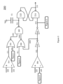
- FIG. 1 illustrates a schematic of an exemplary POR circuit 100, in accordance with embodiments of the present invention.
- the POR circuit 100 comprises of a latch circuit 110, and two comparators 121 and 122.
- the POR circuit 100 comprises the comparators 121 and 122.
- the comparators 121 and 122 are op-amp (operational amplifier), each having an inverting terminal and a non-inverting terminal.
- the output of the comparators 121 and 122 are coupled to the latch circuit 110.
- the non-inverting terminal of the comparator 121 receives a first reference voltage 123 and the inverting terminal of the comparator 121 receives a supply voltage 124. In another embodiment, the inverting terminal of the comparator 121 receives a voltage proportional to the supply voltage. In an embodiment, the non-inverting terminal of comparator 122 receives the supply voltage 125 and the inverting terminal of comparator 122 receives a second reference voltage 126. In one embodiment, the non-inverting terminal of the comparator 121 receives a voltage proportional to the supply voltage.
- the reference voltages 123 and 126 are proportional to a regulator voltage. Any appropriate technique in the art may be used to configure the regulator voltage to produce proportional reference voltages 123 and 126.
- the regulator voltage is generated by a voltage regulator circuit based on a bandgap voltage V BG .
- the bandgap voltage V BG is a constant voltage irrespective of power supply variations, temperature changes and the loading on the device.
- Generating reference voltages 123 and 126 based on the regulator voltage and the bandgap voltage V BG can be performed by any known methods in the art.
- the first reference voltage is greater than the second reference voltage. For example, in case of using POR circuit 100 in radio frequency identification (RFID) systems V BG is 0.365 V, while the first reference voltage is three times the V BG (1.095 V) and the second reference voltage is two times V BG (0.73 V).
- RFID radio frequency identification
- the reference voltages 123 and 126 may have the same voltage; however, the comparators 121 and 122 compare the reference voltages to a voltage proportionate to the supply voltage.
- the reference voltages 123 and 126 may have a same voltage of 0.73 V (double the V BG of 0.365 V), however, the comparator 121 receives a voltage equivalent to two third of the supply voltage and the comparator 122 receives the supply voltage. Any appropriate techniques in the art may be used to generate a voltage proportionate to the supply voltage.
- voltage dividers may be used to generate an appropriate ratio of the supply voltage and the regulator voltage to the comparators 121 and 122.
- voltage dividers may be formed by series connected resistors.
- diode-connected pMos transistors may be used instead of resistors by any known method in the art. The diode-connected pMos transistors provide a lower current through the voltage dividers while accommodating scaling of the device to a smaller size.
- the POR circuit 100 comprises a latch circuit 110.
- the latch circuit 110 is an SR flip-flop formed by two cross-coupled NAND gates 112 and 114.
- the NAND gate 112 receives a de-assert signal 111 from the comparator 121.
- the NAND gate 114 receives a re-assert signal 113 from the comparator 122.
- the output of latch 110 is a POR signal 115.
- the POR signal 115 either de-asserts the reset state or re-asserts the reset state.
- a low POR signal 115 de-asserts the reset state.
- a low de-assert signal 111 and a high re-assert signal 113 is required as inputs to the latch circuit 110.
- a high POR signal 115 re-asserts the reset state.
- a high de-assert signal 111 and a low re-assert signal 113 is required as inputs to the latch circuit 110.
- the POR circuit 100 must begin in an asserting state. Therefore, initially the de-assert signal 111 is at a high state and the re-assert signal 113 is at a low state, resulting in POR signal 115 to be high. Subsequently, as the power-up process progresses, the re-assert signal 113 can be restored to a high state, with the latch 110 output of the POR signal 115 retaining a high state. As the system powers up, the POR circuit 100 must de-assert the reset state when the supply voltage reaches a safe startup voltage and other conditions are met to ensure safe chip operation. In an embodiment, the comparator 121 compares the supply voltage 124 with the first reference voltage 123.
- the de-assert signal 111 switches from a high state to a low state. Therefore, the Latch 110 receives a low de-assert signal 111 and a high re-assert signal 113, generating a low POR signal 115. As such, the POR circuit 100 de-asserts the reset state once the supply voltage reaches a safe threshold.
- the first reference voltage 123 may be set to three times the V BG (0.365 V) at 1.095 V. Therefore, once the startup voltage reaches 1.095V, the POR circuit 100 de-asserts the reset state.
- the second reference voltage 126 may be set to two times the V BG (0.365 V) at 0.73 V. Therefore, if the voltage reaches above 1.095 V it will definitely not be below 0.73 V and the comparator 122 generates a high re-assert signal 113. Receiving a low de-assert signal 111 and a high re-assert signal 113, the latch circuit 110 generates a low POR signal 115. A low POR signal 115 de-asserts the reset state. The reset state will remain de-asserted until POR circuit 100 re-asserts the reset state.
- the first reference voltage 123 must be set to a threshold level that avoids reset cycling of the POR circuit 100. Reset cycling occurs when the device goes through a reset sequence, and the same or related reset event occurs again, thereby causing a new reset sequence to start. In a RFID system, setting the first reference voltage 123 to be three times the V BG will prevent occurrence of reset cycling.
- the comparator 122 compares the supply voltage 125 to the second reference voltage 126. According to the invention, once the supply voltage 125 falls below the second reference voltage 126, the comparator 122 generates a low re-assert signal 113. Since the second reference voltage 126 is lower than the first reference voltage 123, the comparator 121 generates a high de-assert signal 111. Subsequently, the latch 110 generates a high POR signal 115 to re-assert the reset state.
- the second reference voltage 126 may be set to two times the V BG (0.365 V) at 0.73 V. Therefore, once sufficient RF power is lost and supply voltage falls below 0.73V, the comparator 122 generates a low re-assert signal 113.
- the first reference voltage 123 may be set to three times the V BG (0.365 V) at 1.095 V. Therefore, if the supply voltage falls below 0.73V it will definitely fall below 1.095 V and the comparator 121 generates a high de-assert signal 111.
- the latch circuit 110 receives a high de-assert signal 111 and a low re-assert signal 113, the latch circuit 110 generates a high POR signal 115.
- a high POR signal 115 re-asserts the reset state. The reset state will remain asserted until POR circuit 100 de-asserts the reset state as described above.
- FIG. 2 illustrates a more detailed schematic of an exemplary POR circuit 200, in accordance with embodiments of the present invention. It will be appreciated that for simplicity and/or clarity of illustration, some elements of the invention are described in other figures as referenced in figure 2 .
- the POR circuit 200 must begin in an asserting state until the conditions are met for the de-assertion of the reset signal.
- a de-assert1 signal 211 to the NAND gate 112 must be at a high state while a re-assert1 signal 213 to the NAND gate 114 must begin low.
- the re-assert signal 213 will transition to a high state as the system powers up.
- a capacitor C1 is placed between the supply voltage V dd and the de-assert1 signal 211. As such, during the system power up, the voltage of the de-ssert1 signal 211 follows the V dd voltage as the capacitor C1 charges up.
- the circuit in figure 3 may be used.
- voltage regulators may use V BG to generate the reference voltages 123 and 126.
- V BG voltage regulators
- some bandgap circuits and voltage regulators behave somewhat erratically during power-up with very different behaviors under different startup conditions and power-up rates.
- the POR circuit 200 must ensure to block de-assertion of the reset state until voltages of regulators and bandgap are stabilized.
- the circuit in figure 4 may be used to determine whether the stabilization point has been reached. As further explained blow, to block the de-assertion, the circuit of figure 4 generates a high blocking signal 411.
- the POR circuit 200 must also block de-assertion if the reference voltages 123 and 126 are too low.
- the bandgap voltage may take some time to rise and consequently the reference voltages 123 and 126 may be at a ground level initially.
- the circuit of figure 4 blocked a de-assertion of the reset state before the regulator voltages V REG are stabilize, the circuit of figure 5 ensures to block premature de-assertion when the reference voltages are too low.
- the circuit of figure 5 generates a high blocking signal 511.
- the de-assert1 signal 211 in order to re-assert the reset state once the supply voltage 125 falls below the second reference voltage 126, the de-assert1 signal 211 must be at a high state.
- logic gates may be used to ensure the de-assert1 signal 211 is at a high state when the re-assert1 signal is at a low state.
- NOR gate 202 in combination with a NAND gate 203 may be used.
- the NOR gate 202 receives the output signal 1205 of the inverter 205 and the blocking signal 511.
- the output signal 1202 of the NOR gate 202 is inputted to the NAND gate 203.
- the signal 113 goes to a low state.
- the NOR gate 202 receives a high signal 1205 through the inverter 205. Subsequently, irrespective of the state of the signal 511, the output signal 1202 of the NOR gate 202 will be low. Because of the low state of the output signal 1202 to the NAND gate 203, the de-assert1 signal 211 will be high regardless of the state of the signal 1201.
- logic gates may be used to block the de-assertion based on the signal generated by the circuits of figure 4 and figure 5 .
- the NOR gate 201 receives the blocking signal 411 and the de-assert signal 111.
- the NOR gate 202 receives the blocking signal 511 and the signal 1205.
- the output 1201 of the NOR gate 201 and the output 1202 of the NOR gate 202 are inputted to the NAND gate 203.
- the de-assert1 signal 211 of the NAND gate 203 must be low.
- the de-assert1 signal 211 will be low only when both signals 1201 and 1202 to the NAND gate 203 are high.
- the output signals 1201 and 1202 of the NOR gates 201 and 202 are high if all input signals 111, 411, 511, and 1205 are at a low state. Therefore, as explained above, the circuit of figure 4 and the circuit of figure 5 can block de-assertion of the reset state by generating high blocking signals 411 and 511.
- the comparator 204 compares the supply voltage 125 to the second reference voltage 126 to ensure re-assertion of the reset state once the supply voltage falls below a threshold level.
- the reference voltage 126 is based on the V BG , and V BG drops as the supply voltage 125 falls, the re-assertion may be never be initialized.
- the circuit of figure 6 generates a stored version of the reference voltage 126. The time for which the stored version is held is sufficient for the comparator 122 to recognize the supply voltage is dropping below a threshold level to re-assert the reset state.
- the bandgap circuit may use a control voltage to generate a regulated current.
- This control voltage can be used with techniques such as current mirroring to generate multiple temperature independent currents for use in circuits other than the bandgap circuit.
- the control voltage is initially at zero but it increases as the system powers up.
- the control voltage of the bandgap circuit described in a related US Patent Application No._____ (Attorney docket number 003424.P117) entitled "Fractional Bandgap With Low Supply Voltage and Low Current" by Inventors William Schnaitter and Steve Wang filed______ is used in this invention.
- a control voltage may be any generally stable voltage that can be used with a circuit to provide stable operation of the circuit, such as a POR circuit, and this generally stable voltage can be used to generate a regulated current.
- the circuit 300 ensures that the POR circuit 200 of figure 2 is in an asserting state by setting the voltage of the re-assert1 signal 213 at a low state as the system powers up.
- the circuit 300 comprises of a capacitor C2 coupled to a voltage source V dd and a drain of a transistor M2 at a node XX.
- a gate of the transistor M2 is coupled to a control voltage 301.
- a source of the transistor M2 is coupled to the ground.
- the circuit 300 also comprises of another transistor M1, having its drain coupled to a node ZZ, a gate connected to the node XX, and a source coupled to the ground.
- a capacitor C3 is coupled in parallel with the transistor M1, having one terminal connected to the node ZZ and the other terminal grounded.
- the node ZZ is coupled to the re-assert1 signal 213, between the inverter 206 and the comparator 114 as illustrated in figure 2 .
- the transistor M1 and M2 are N-type Metal Oxide Semiconductor (NMOS) transistors.
- the capacitor C2 begins charging by the voltage source V dd during the system startup.
- the voltage at the node XX initially follows V dd .
- the transistor M1 will begin to conduct.
- the transistor M1 pulls the voltage of the node ZZ to the ground level. Consequently, the re-assrt1 signal 213 inputs a low state to the latch 110 of figure 2 .
- a low re-assert1 signal 213 results in a high PoR signal 115 and asserting the reset state.
- the bandgap voltage increases from a ground level to a constant threshold.
- the signal 301 is the control voltage to generate a regulated current, used in the bandgap circuit.
- the control voltage is initially at zero but it increases as the system powers up.
- the control signal 301 will rise to turn on the M2 transistor.
- the M2 transistor pulls the voltage at the XX node to the ground level and the transistor M1 will stop conducting any further. Consequently, the state of the re-assrt1 signal 213 is dictated by the output of the inverter 206 in figure 2 .
- the circuit 400 ensures to block the de-assertion of the reset state until the regulator voltage V REG and the bandgap voltage are stabilized.
- the circuit 400 comprises of three transistors M3, M4, and M5, a capacitor C4, and a comparator 420.
- the transistor M3 and M4 are P-type Metal Oxide Semiconductor (PMOS) transistors.
- the transistors M3 and M4 form a current mirror in the following configuration: gates of the transistors M3 and M4 are coupled together, sources of the transistors M3 and M4 are coupled to a regulator voltage V REG , and the M3 transistor will be forced to sustain a current dictated by M5 and node 401.
- the transistor M3 is matched to the transistor M4, that is, the PMOS transistors have the same characteristics.
- the V GS (Gate-Source Voltage) of the transistor M3 is set to the V GS of the transistor M4, and consequently, a current I REF flowing in the drain of the transistor M3 is the same as the current I OUT flowing in the drain of the transistor M4.
- the bulk terminal of the transistors M3 and M4 is coupled to the supply voltage V dd .
- the drain of the transistor M3 is also coupled to the drain of transistor M5.
- the current in transistor M5 is controlled by a control voltage 401.
- a control voltage is used generate a regulated current in the bandgap circuit. The control voltage is initially at zero but it increases as the system powers up.
- the transistor M5 is a NMOS transistor.
- the drain of the transistor M4 is coupled to the capacitor C4. The other terminal of the capacitor C4 is grounded.
- a delayed replica of the regulator voltage V REG is generated at a terminal 402 connecting the capacitor C4 to the drain of the transistor M4 and to the inverting terminal of the comparator 420.
- a non-inverting terminal of the comparator 420 is coupled to a regulator voltage 403.
- the comparator 420 is an Operational Amplifier (OPAMP).
- the comparator 420 generates a blocking signal 411.
- control voltage 401 is near the ground level. As the system powers up and the supply voltage V dd rises, the control voltage 401 from the bandgap circuit and the regulator voltage 403 will also increase. However, as it will be further discussed below, the delayed regulator voltage 402 will initially remain low. Subsequently, the comparator 420 generates a high blocking signal 411.
- the transistor M5 starts conducting.
- relatively small current I REF from the transistor M5 to M3 is mirrored as a current I OUT from the drain of the transistor M4.
- the mirrored current I OUT may be a very low current, for example about 6 nano-amp.
- the current I OUT starts charging the capacitor C4.
- the size of the capacitor C4 determines accurately the time it takes for the delayed regulator voltage 402 to reach a voltage very close to V REG of the regulator voltage 403.
- the size of the capacitor C4 is determined based on the time required for the regulator voltage V REG and the bandgap voltage to stabilize. Once the delayed regulator voltage 402 reaches the V REG of the regulator voltage 403, the comparator 420 generates a low blocking signal 411.
- the comparator 420 can be designed to have an offset voltage in the differential input level.
- the comparator offset voltage represents the minimum direct current (DC) input voltage that would have to be applied to input terminals of the comparator to cause the comparator to transition state.
- the offset voltage guarantees that the blocking signal 411 goes to a low state once the delayed regulator voltage 402 reaches within an acceptable range of V REG .
- the offset voltage of the comparator 420 can be configured using an integral-ratioed asymmetry in the op-amp differential input transistor pair, or by other known techniques in the art. For example, in case the POR circuit 200 is used in an RFID system, the comparator 420 could be modified to generate a low blocking signal 411 when the delayed regulator voltage 402 is within 20-50 mV of the V REG .
- the circuit 400 discussed above compares a delayed replica of the regulator voltage with the regulator voltage V REG to ensure its stability before allowing for the de-assertion of the PoR circuit.
- both the delayed regulator voltage 402 and the regulator voltage 403 are close to a ground level.
- the comparator 420 recognizes the voltage levels of the two signals are very close and generates a low blocking signal 411. Consequently, the circuit 400 may wrongfully allow the de-assertion of the reset state.
- the circuit 500 is used.
- the circuit 500 blocks de-assertion of the reset state when the regulator voltage V REG is too low.
- the circuit 500 comprises of four transistors M6, M7, M8, and M9; a series of resistors R1, R2, and R3; a capacitor C7; and two inverters 521 and 522.
- the transistor M6 and M7 are PMOS transistors.
- the transistors M6 and M7 form a current mirror in the following configuration: gates of the transistors M6 and M7 are coupled together, sources of the transistors M6 and M7 are coupled to the source voltage V dd .
- the transistor M6 is matched to the transistor M7, that is, the PMOS transistors have the same characteristics.
- the V GS of the transistor M6 is set to the V GS of the transistor M7, and consequently, a current flowing in the drain of the transistor M6 is the same as the current flowing in the drain of the transistor M7.
- the drain of the transistor M6 is coupled to a drain of the transistor M8.
- a source of the transistor M8 is grounded.
- a gate of the transistor M8 is coupled to a control voltage 501.
- a control voltage is used to generate a regulated current in the bandgap circuit. The control voltage is initially at zero but it increases as the system powers up.
- a drain of the transistor M9 is coupled to the drain of transistor M7.
- a source of the transistor M9 is grounded.
- a gate of the transistor M9 receives a divided regulator voltage 502.
- the divided regulator voltage 502 is generated by a voltage divider 520.
- the voltage divider 520 is formed by a series of resistors R1, R2, and R3 coupled between a regulator voltage V REG and a ground voltage.
- the blocking signal 511 is generated on a node YY after going through two inverters 522 and 521.
- the node YY is the terminal connecting the drain of the transistor M7 to the drain of the transistor M9.
- the capacitor C7 is coupled between the source voltage V dd and the node YY.
- the capacitor C7 ensures that the voltage of the node YY also increases. Also as the voltage source V dd rises the control voltage 501 increases. The control voltage 501 turns on the transistor M8.
- relatively small current I REF from the transistor M8 to M6 is mirrored as a current I OUT from the drain of the transistor M7 to the source of M9.
- the mirrored current I OUT may be about 6 nano-amp.
- a high state of the node YY is buffered by the inverters 522 and 521generating a high blocking signal 511. The high blocking signal 511 will block the de-assertion of the reset state, as long as V REG remains very low, close to ground.
- the transistor M9 is controlled by signal 502 of the voltage divider 520. While the regulator voltage V REG is low, M9 is off. Once a ratio of the regulator voltage V REG set by the voltage divider 520 reaches the conduction threshold of the transistor M9, the M9 transistor begins conducting. In an embodiment, once the M9 starts conducting, the current in M9 will become much greater than the small regulated current I OUT . Subsequently the voltage on the node YY will be pulled to the ground level. In an embodiment, two third of V REF is required to reach the conduction threshold of the transistor M9. The low state of the node YY is buffered by the inverters 522 and 521, generating a low blocking signal 511. The low blocking signal ceases blocking the de-assertion of the PoR circuit.
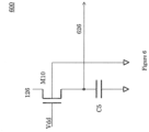
- the circuit 600 generates a stored version of the second reference voltage 126 of figure 1 for the comparator 122.
- the bandgap voltage is used to generate regulator voltage.
- the reference voltages are proportional to the regulator voltage.
- the bandgap voltage is advantageously capable of operating with a low power supply potential.
- the comparator 122 compares the supply voltage 125 to the second reference voltage 126. Once the supply voltage 125 falls below the second reference voltage 126, the comparator 122 generates a low re-assert signal 113 to re-assert the reset state.
- the bandgap voltage also declines.
- the behavior of the bandgap voltage depends upon variations in process, temperature and ramp-down rate of V dd .
- the bandgap voltage may start to fail at a nearby V dd level and the second reference voltage 126 may rapidly decline well below V dd . As such, the supply voltage 125 may never drop below the second reference voltage 126 for the re-assertion to occur.
- the circuit 600 generates a stored version of the second reference voltage 126, a stored reference voltage 626, for the comparator 204 of figure 2 .
- the circuit 600 comprises of an NMOS transistor M10 and a capacitor C5.
- a drain of the transistor M10 is coupled to the second reference voltage 126, a source of the transistor M10 is coupled to the capacitor C5, a bulk terminal of the transistor M10 is grounded, and a gate of the transistor M10 is coupled to the supply voltage V dd .
- the stored reference voltage 626 is generated at a node coupling the capacitor C5 to the source of the transistor M10. The other terminal of the capacitor C5 is grounded.
- the transistor M10 while the system is powered up and the supply voltage V dd exceeds the threshold for de-assertion of the PoR signal, the transistor M10 is turned on. Consequently, the capacitor C5 is charged through the transistor M10 to the same voltage level as the second reference voltage 126. In an embodiment, as the chip is powered down and V dd falls close to the second reference voltage 126, the transistor M10 conducts at a very low rate. However, because of the charged capacitor C5, the voltage level of the stored reference voltage 626 will remain unchanged in the time scale of chip power down. When the supply voltage 125 of the figure 2 falls below the stored reference voltage 626, the comparator 122 will flip the latch 110 to re-assert the reset state.
- the comparator 122 can be designed to have an offset voltage in the differential input level.
- the comparator offset voltage represents the minimum direct current (DC) input voltage that would have to be applied to input terminals of the comparator to cause the comparator to transition state.
- the offset voltage of the comparator 122 can be configured using an integral-ratioed asymmetry in the op amp differential input transistor pair, or by other known techniques in the art.
- the comparator 122 is configured to push a re-assertion voltage at a voltage level lower than the stored reference voltage 626.
- the comparator 122 could be modified to push the re-assertion voltage when the supply voltage 125 is within 20-50 mV below the stored reference voltage 626.
- the reassertion voltage is pushed when the supply voltage 125 is around 0.7V or slightly lower.
- the POR circuit 200 described above could be used to perform other functionalities in a chip.
- the circuit can determine when the supply voltage V dd is greater than a reference voltage and when it falls below certain other reference voltage.
- a first comparator compares the supply voltage V dd to three times the bandgap voltage V BG
- a second comparator compares the supply voltage V dd to twice the bandgap voltage V BG .
- the reference voltage can be modified to set different threshold. For example, various circuits within a chip that may not be reliable at some voltage levels can be disabled to prevent incorrect operations.
- a series of resistors are used to adjust the level of reference voltage input to the comparators.
- an accurate adjustment is possible by drawing a known current from the voltage regulator through a known resistor to provide the reference voltage inputted to the comparators.
- the current may be mirrored in some ratio from a known regulated current from a bandgap circuit or other reference voltage circuits.
- the resistors may match those resistors in a bandgap circuit as well.
- the resistors can be segmented to allow a wide range of voltage adjustment of the comparator input by tapping off any node between resistor segments desired.
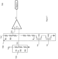
- the circuit 700 comprises of the voltage divider 720 generating input signal 721 to an inverting terminal of the comparator 712 and the circuit 730 generating a reference signal 731 to a non-inverting terminal of the comparator 712.
- the voltage divider 720 comprises of a plurality of resistors.
- the voltage divider 720 comprises of resistors R1, R2, and R3.
- the resistors R1, R2, and R3 have a same resistance.
- a different ratio of the supply voltage V dd is generated depending on which terminal of the voltage divider 720 the comparator 712 is coupled to.
- the input signal 721 has two third voltage of the supply voltage V dd .
- circuit 730 may be configured to adjust a reference voltage 731 to a non-inverting terminal of the comparator 712.
- the circuit 730 comprises of a plurality of resistors (R1, R2, ..., Rn) coupled in series with two transistors M21 and M22 between the reference voltage V REF and ground.
- a gate of the transistor M21 is coupled to an enabling signal 702.
- a gate of the transistor M22 is coupled to the control voltage 710.
- the circuit 730 generates a reference signal 731.
- the non-inverting terminal of the comparator 712 is coupled to one of the terminals between the resistors R1 through Rn.
- the voltage on the reference signal 731 depends upon which terminal between the two resistors in series of resistors R1 through Rn the comparator 712 is coupled to.
- the comparator 712 when the enabling signal 702 is set to a ground level, the comparator 712 functions the same as previously described with respect to the comparator 121 of figure 1 .
- the series of resistors R1 through Rn pull the non-inverting terminal of the comparator 712 up to the voltage reference V REF .
- the de-assertion could take place according to the procedure explained above.
- the enabling signal 702 could turn on the transistor M21.
- the control voltage is pushing a known current through the transistor M22. The current will go through certain number of resistors R1 through Rn, forcing the reference signal 731 to be lower than the reference voltage V REF .
- the increase in the output of the comparator 712 will not impact the behavior of the POR circuit 200 since the de-assertion has already taken place.
- other chip logics of the system can be sensing a logic high voltage in an output signal 111.
- other sensitive circuitry in the chip which might operate improperly at or below the voltage sensed by the circuit 700, may be disabled.
- a non-volatile memory may operate well at 0.85 V; however, its write functionality can be corrupted at or below 0.8 V.
- the output signal 111 of the comparator 712 will go to a high state (very close to V dd ) when the input signal 721 is below the reference signal 731.
- the output signal 111 of the comparator 712 will go to a low state (very close to the ground) when the input signal 721 is above the reference signal 731.
- the comparator 712 will send a disabling high output signal 111 if: 2 / 3 V dd ⁇ V ref ⁇ I M22 ⁇ R 1 + R 2 + ... + R j
- non-inverting input of 712 is connected to the circuit730 between R n and R n+1 and I M22 is the current going through the transistor M22.
- the series resistors R1 through R n+1 allow the adjustment of the reference signal 731.
- an analog mux may be placed between the terminals and the non-inverting terminal of the comparator 712. Subsequently, the adjustment to the reference signal 731 could be made using control circuitry.
- FIG. 8 is a flow chart explaining the operation of the POR circuit in accordance with one embodiment of the invention.
- the POR circuit begins its operation at step 810 by having the system in an asserted state.
- the system remains in an asserted state until the conditions for de-assertion are met.
- any appropriate startup circuit may be used to generate signals placing the system initially in an asserted state.
- the circuit of figure 3 explained above is used to initiate the POR circuit in an asserted state.
- the POR circuit determines whether the supply voltage V dd is above a threshold level for a safe de-assertion of the system.
- the threshold level is defined by a first reference voltage V REF1 .
- the V REF1 is generated by voltage regulators based on a bandgap voltage V BG .
- any appropriate circuit may be used to compare the reference voltage V REF1 to the supply voltage V dd .
- a first comparator of figure 2 is used to compare V REF1 to V dd . If the supply voltage V dd is above the threshold set by the first reference voltage V REF1 the step 830 is implemented, otherwise the POR circuit will remain asserted until the conditions are met.
- the POR circuit determines whether the bandgap voltage V BG and regulator voltage V REG are in a stable state.
- the regulator voltage V REG is generated by a voltage regulator based on the bandgap voltage V BG .
- a delayed version of the V REG is compared to the V REG . If the voltages are substantially the same, the regulator voltage has stabilized. Any appropriate circuitry can be used to generate a delayed version of the regulator voltage and to compare the delayed regulator voltage to the regulator voltage.
- the circuit of figure 4 is used to generate a delay version of V REG and to compare it to the V REG . If the bandgap voltage V BG and the regulator voltage V REG have stabilized the step 840 of the flow chart 800 is implemented, otherwise the POR circuit will remain asserted until the conditions are met.
- the POR circuit determines whether the regulator voltage V REG is too low.
- a delayed version of the regulator voltage V REG is compared to V REG .
- the step 830 will fail.
- step 830 ensures V REG is at a certain voltage for a safe de-assertion.
- Any appropriate circuitry can be used to determine whether V REG is at a low voltage level.
- the circuit of figure 5 is used to determine whether a fraction of V REG is at a conduction voltage level of a transistor. If the V REG is higher than the required threshold, the step 850 of the flow chart 800 is implemented, otherwise the POR circuit will remain asserted until the conditions are met.
- the POR circuit finally de-asserts the reset state.
- the system will remain in the de-assertion state until a condition for re-assertion is met.
- the POR circuit loops between the step 850 and 860 until the re-assertion condition is met.
- the POR circuit determines whether conditions for re-assertion are met. In an embodiment, when the supply voltage V dd falls below a threshold level the system malfunctions. To avoid malfunctioning of the system, a re-assertion of the reset state is enforced when the supply voltage drop below the voltage of a second reference voltage V REF2 . In an embodiment, a second comparator of figure 2 is used to compare V REF2 to V dd . If the supply voltage V dd is below the threshold set by the second reference voltage V REF2 the POR re-asserts the reset state and returns to step 810, otherwise the system will remain in a de-asserted state.
- V REF2 may follow V dd as the system powers down.
- a stored version of V REF2 is used to compare with V dd .
- Any appropriate circuit may be used to generate a stored version of V REF2 .
- the circuit of figure 6 is used to generate a stored version of V REF2 .
Landscapes
- Physics & Mathematics (AREA)
- Nonlinear Science (AREA)
- Electronic Switches (AREA)
Claims (10)
- Power-On-Reset-Schaltung (100), die so konfiguriert ist, dass sie ein Power-On-ResetSignal, POR-Signal (115), erzeugt, umfassend:einen ersten Komparator (121) mit einem ersten Eingangsanschluss, einem zweiten Eingangsanschluss und einem Ausgangsanschluss, wobei der erste Eingangsanschluss mit einer ersten Referenzspannung (123) und der zweite Eingangsanschluss mit einer ersten Spannung (124), die proportional zu einer Versorgungsspannung (Vdd) ist, gekoppelt ist;einen zweiten Komparator (122) mit einem ersten Eingangsanschluss, einem zweiten Eingangsanschluss und einem Ausgangsanschluss, wobei der erste Eingangsanschluss mit einer zweiten Spannung (125), die proportional zu der Versorgungsspannung (Vdd) ist, gekoppelt ist und der zweite Eingangsanschluss mit einer zweiten Referenzspannung (126) gekoppelt ist, wobei die erste und die zweite Referenzspannung proportional zu einer Reglerspannung sind; undeine Latch-Schaltung (110), die ein erstes NAND-Gatter (112) mit einem ersten Eingangsanschluss, einem zweiten Eingangsanschluss und einem Ausgang sowie ein zweites NAND-Gatter (114) mit einem ersten Eingangsanschluss, einem zweiten Eingangsanschluss und einem mit dem zweiten Anschluss des ersten Gatters kreuzgekoppelten Ausgang umfasst, wobei der Ausgangsanschluss des ersten Komparators (121) mit dem ersten Eingangsanschluss des ersten Gatters (112) gekoppelt ist, der Ausgangsanschluss des zweiten Komparators (122) mit dem zweiten Eingangsanschluss des zweiten Gatters (114) gekoppelt ist, und der Ausgang des ersten Gatters (112) mit dem ersten Eingangsanschluss des zweiten Gatters (114) der Latch-Schaltung gekoppelt ist, wobei der Ausgang des zweiten Gatters (114) mit dem zweiten Eingangsanschluss des ersten Gatters (112) gekoppelt ist, um das POR-Signal als ein De-Assert-Signal (115) zu erzeugen, um einen Rücksetzzustand als Reaktion auf den Anstieg der ersten Spannung über die erste Referenzspannung zu de-assertieren, sobald die Versorgungsspannung einen ersten Schwellenwertpegel erreicht, und um das POR-Signal als ein Re-Assert-Signal (115) zu erzeugen, um den Rücksetzzustand als Reaktion auf das Abfallen der zweiten Spannung unter die zweite Referenzspannung erneut zu assertieren, sobald die Versorgungsspannung unter einen zweiten Schwellenwertpegel fällt; undeine Speicherschaltung (600), wobei die Speicherschaltung einen NMOS-Transistor (M10) und einen Kondensator (C5) umfasst, wobei der Transistor (M10) einen Drain, der mit der zweiten Referenzspannung (126) gekoppelt ist, einen Bulk-Anschluss des Transistors (M10), der geerdet ist, ein Gate, das mit der Versorgungsspannung (Vdd) gekoppelt ist, und eine Source aufweist, die mit dem Kondensator (C5) gekoppelt ist, wobei, wenn die Versorgungsspannung (Vdd) den ersten Schwellenwert überschreitet, der NMOS-Transistor (M10) eingeschaltet wird, wodurch der Kondensator (C5) durch den NMOS-Transistor (M10) auf den gleichen Spannungspegel wie die zweite Referenzspannung (126) geladen wird, um eine gespeicherte Version der zweiten Referenzspannung (126) zu speichern.
- Power-On-Reset-Schaltung nach Anspruch 1, wobei die erste Referenzspannung größer ist als die zweite Referenzspannung und wobei die erste Referenzspannung und die Reglerspannung auf der Grundlage einer Bandlückenspannung erzeugt werden.
- Power-On-Reset-Schaltung nach Anspruch 1, wobei vor der Erzeugung des De-Assert-Signals durch die Latch-Schaltung der Rücksetzzustand aktiviert wird.
- Power-On-Reset-Schaltung nach Anspruch 1 ferner umfassend eine Startschaltung (300), die Folgendes umfasst:einen ersten Kondensator (C2), der zwischen der Versorgungsspannung und einem ersten Transistor (M2) angeschlossen ist;wobei der erste Transistor einen Drain, der mit dem ersten Kondensator verbunden ist, eine Source, die geerdet ist, und ein Gate aufweist, das mit einer Steuerspannung (301) verbunden ist;einen zweiten Transistor (M1), dessen Drain mit dem ersten Anschluss der Latch-Schaltung (213) verbunden ist, dessen Source geerdet ist und dessen Gate mit dem Drain des ersten Transistors (M2) verbunden ist; undeinen zweiten Kondensator (C3), der zwischen den ersten Anschluss der Latch-Schaltung (213) und die Masse geschaltet ist.
- Power-On-Reset-Schaltung nach Anspruch 2, wobei das De-Assert-Signal so konfiguriert ist, dass es verzögert wird, bis die Reglerspannung stabilisiert ist.
- Power-On-Reset-Schaltung nach Anspruch 5, bei der eine verzögerte Version der Reglerspannung mit der Reglerspannung verglichen wird und ferner umfassend eine erste De-Assert-Blockierschaltung (400).
- Power-On-Reset-Schaltung nach Anspruch 2, wobei das De-Assert-Signal so konfiguriert ist, dass es verzögert wird, bis die Reglerspannung wesentlich über einer Massespannung liegt.
- Power-On-Reset-Schaltung nach Anspruch 7 ferner umfassend eine zweite De-Assert-Blockierschaltung (500), die Folgendes umfasst:einen ersten Transistor (M6) mit einer Source, die mit der Versorgungsspannung verbunden ist, einem Gate, das mit einem Gate des zweiten Transistors (M7) verbunden ist, und einem Drain, der mit dem Gate und einem dritten Transistor (M8) verbunden ist;einen zweiten Transistor (M7) mit einer Source, die mit der Versorgungsspannung verbunden ist, einem Gate, das mit dem Gate des ersten Transistors (M6) verbunden ist, und einem Drain, der mit einem vierten Transistor (M9) verbunden ist;einen dritten Transistor (M8) mit einem Drain, der mit dem Drain des ersten Transistors (M6) gekoppelt ist, einer Source, die auf Masse liegt, und einem Gate, das mit einer Steuerspannung (501) verbunden ist;einen vierten Transistor (M9) mit einem Drain, der mit dem Drain des zweiten Transistors (M7) gekoppelt ist, einer Source, die geerdet ist, und einem Gate, das mit einem Spannungsteiler (520) gekoppelt ist, wobei der Spannungsteiler einen Bereich für die Reglerspannung über der Masse definiert, um die Erzeugung des De-Assert-Signals zu ermöglichen;wobei der Spannungsteiler (520) mit der Reglerspannung und einer Masse verbunden ist;einen Kondensator (C7), der zwischen der Stromversorgung und dem Drain des zweiten Transistors angeschlossen ist; undein Ausgangssignal, das an einem Anschluss (YY) erzeugt wird, der den Drain des zweiten Transistors (M7) und den Drain des vierten Transistors (M9) koppelt.
- Power-On-Reset-Schaltung nach Anspruch 2, wobei die zweite Referenzspannung eine gespeicherte Version der Reglerspannung ist.
- Power-On-Reset-Schaltung nach Anspruch 9, wobei
nach der Erzeugung des De-Assert-Signals das erste Referenzsignal auf einen anderen Spannungspegel geändert wird.
Applications Claiming Priority (2)
| Application Number | Priority Date | Filing Date | Title |
|---|---|---|---|
| CN201510523813.3A CN106487367A (zh) | 2015-08-24 | 2015-08-24 | 上电复位电路,及产生上电复位信号的方法 |
| US14/845,246 US9515637B1 (en) | 2015-08-24 | 2015-09-03 | Power-on reset circuit |
Publications (3)
| Publication Number | Publication Date |
|---|---|
| EP3136601A1 EP3136601A1 (de) | 2017-03-01 |
| EP3136601B1 true EP3136601B1 (de) | 2024-08-07 |
| EP3136601C0 EP3136601C0 (de) | 2024-08-07 |
Family
ID=57400032
Family Applications (1)
| Application Number | Title | Priority Date | Filing Date |
|---|---|---|---|
| EP16001858.6A Active EP3136601B1 (de) | 2015-08-24 | 2016-08-24 | Power-on-reset-schaltung |
Country Status (3)
| Country | Link |
|---|---|
| US (1) | US9515637B1 (de) |
| EP (1) | EP3136601B1 (de) |
| CN (1) | CN106487367A (de) |
Families Citing this family (11)
| Publication number | Priority date | Publication date | Assignee | Title |
|---|---|---|---|---|
| US10256809B2 (en) * | 2015-08-24 | 2019-04-09 | Ruizhang Technology Limited Company | Power-on reset circuit |
| US20200285780A1 (en) * | 2019-03-06 | 2020-09-10 | Nvidia Corp. | Cross domain voltage glitch detection circuit for enhancing chip security |
| US20210294410A1 (en) * | 2019-03-06 | 2021-09-23 | Nvidia Corp. | Circuit Solution for Managing Power Sequencing |
| WO2021075150A1 (ja) | 2019-10-18 | 2021-04-22 | 富士電機株式会社 | フィルタ回路及び半導体装置 |
| CN110932704B (zh) * | 2019-12-12 | 2022-12-02 | 中国科学院微电子研究所 | 一种上电电路及电荷泵电路 |
| CN112558674B (zh) * | 2020-12-02 | 2023-02-21 | 浙江中控技术股份有限公司 | 一种模拟量电流输出系统 |
| CN113810032B (zh) * | 2021-09-24 | 2023-08-22 | 电子科技大学 | 一种上电复位电路结构 |
| US12222747B2 (en) * | 2022-04-01 | 2025-02-11 | Texas Instruments Incorporated | Methods and apparatus to facilitate safe startup of a power management unit |
| CN115483917B (zh) * | 2022-08-19 | 2025-07-08 | 温州大学 | 一种低功耗上电复位电路 |
| CN117118417B (zh) * | 2023-09-26 | 2025-08-29 | 北京昂瑞微电子技术股份有限公司 | 电源上电复位电路 |
| US20250202475A1 (en) * | 2023-12-15 | 2025-06-19 | Nxp B.V. | Power-on reset circuit |
Citations (3)
| Publication number | Priority date | Publication date | Assignee | Title |
|---|---|---|---|---|
| US20140118040A1 (en) * | 2012-10-31 | 2014-05-01 | Lapis Semiconductor Co., Ltd. | Synchronizing circuit and clock data recovery circuit including the same |
| US20160308566A1 (en) * | 2012-12-27 | 2016-10-20 | Intel Corporation | High speed receivers circuits and methods |
| US9912309B1 (en) * | 2015-05-27 | 2018-03-06 | Marvell Israel (M.I.S.L.) Ltd. | Filter-less chopping for offset cancellation |
Family Cites Families (5)
| Publication number | Priority date | Publication date | Assignee | Title |
|---|---|---|---|---|
| US5369310A (en) * | 1992-06-01 | 1994-11-29 | Hewlett-Packard Corporation | CMOS power-on reset circuit |
| KR100854419B1 (ko) * | 2007-03-31 | 2008-08-26 | 주식회사 하이닉스반도체 | 파워 업 신호 생성장치 |
| US7639052B2 (en) * | 2007-04-06 | 2009-12-29 | Altera Corporation | Power-on-reset circuitry |
| JP6118599B2 (ja) * | 2013-03-19 | 2017-04-19 | 富士通株式会社 | パワーオンリセット回路、電源回路および電源システム |
| CN103532531A (zh) * | 2013-10-12 | 2014-01-22 | 中山大学 | 一种上电复位电路及方法 |
-
2015
- 2015-08-24 CN CN201510523813.3A patent/CN106487367A/zh active Pending
- 2015-09-03 US US14/845,246 patent/US9515637B1/en active Active
-
2016
- 2016-08-24 EP EP16001858.6A patent/EP3136601B1/de active Active
Patent Citations (3)
| Publication number | Priority date | Publication date | Assignee | Title |
|---|---|---|---|---|
| US20140118040A1 (en) * | 2012-10-31 | 2014-05-01 | Lapis Semiconductor Co., Ltd. | Synchronizing circuit and clock data recovery circuit including the same |
| US20160308566A1 (en) * | 2012-12-27 | 2016-10-20 | Intel Corporation | High speed receivers circuits and methods |
| US9912309B1 (en) * | 2015-05-27 | 2018-03-06 | Marvell Israel (M.I.S.L.) Ltd. | Filter-less chopping for offset cancellation |
Also Published As
| Publication number | Publication date |
|---|---|
| EP3136601A1 (de) | 2017-03-01 |
| CN106487367A (zh) | 2017-03-08 |
| US9515637B1 (en) | 2016-12-06 |
| EP3136601C0 (de) | 2024-08-07 |
Similar Documents
| Publication | Publication Date | Title |
|---|---|---|
| EP3136601B1 (de) | Power-on-reset-schaltung | |
| US10256809B2 (en) | Power-on reset circuit | |
| US9046910B2 (en) | Constant current generation circuit and microprocessor including the same | |
| US6052006A (en) | Current mirror triggered power-on-reset circuit | |
| KR100301368B1 (ko) | 파워온리셋회로 | |
| US10429417B2 (en) | Brown-out detectors | |
| EP2897021B1 (de) | Verfahren und Vorrichtung für Gleichstromwandler mit Verstärkung/Low-Dropout (LDO) | |
| US20150042386A1 (en) | Highly accurate power-on reset circuit with least delay | |
| CN112825004B (zh) | 低压差稳压器以及调节低压差稳压器的方法 | |
| CN108023581B (zh) | 小面积低功率上电复位电路 | |
| KR20090068728A (ko) | 기준 전압 발생 회로를 위한 기동 회로 | |
| US20190050011A1 (en) | Regulator circuit | |
| CN110391805B (zh) | 复位电路上的低静态电流功率 | |
| WO2022010728A1 (en) | A voltage-glitch detection and protection circuit for secure memory devices | |
| KR100724662B1 (ko) | 파워 온 리셋 신호를 생성하는 반도체 장치 | |
| US11630161B1 (en) | Flexible circuit for droop detection | |
| US20040263222A1 (en) | Power-on reset circuit with supply voltage and temperature immunity, ultra-low DC leakage current, and fast power crash reaction | |
| US10382033B2 (en) | Stress tolerant power supply voltage detector circuit operable over a wide range of power supply voltages | |
| US11705902B2 (en) | Supply voltage detecting circuit and circuit system using the same | |
| US20140266308A1 (en) | Clock amplitude detection | |
| US20050141287A1 (en) | Power-up circuit in semiconductor memory device | |
| US9712154B1 (en) | Voltage generation circuit and integrated circuit including the same | |
| US8253452B2 (en) | Circuit and method for powering up an integrated circuit and an integrated circuit utilizing same | |
| KR20120103001A (ko) | 파워 온 리셋 회로 및 그것을 포함하는 전자 장치 | |
| JP2011188361A (ja) | パワーオンリセット回路 |
Legal Events
| Date | Code | Title | Description |
|---|---|---|---|
| PUAI | Public reference made under article 153(3) epc to a published international application that has entered the european phase |
Free format text: ORIGINAL CODE: 0009012 |
|
| STAA | Information on the status of an ep patent application or granted ep patent |
Free format text: STATUS: THE APPLICATION HAS BEEN PUBLISHED |
|
| AK | Designated contracting states |
Kind code of ref document: A1 Designated state(s): AL AT BE BG CH CY CZ DE DK EE ES FI FR GB GR HR HU IE IS IT LI LT LU LV MC MK MT NL NO PL PT RO RS SE SI SK SM TR |
|
| AX | Request for extension of the european patent |
Extension state: BA ME |
|
| RIN1 | Information on inventor provided before grant (corrected) |
Inventor name: SCHNAITTER, WILLIAM Inventor name: WANG, STEVE |
|
| STAA | Information on the status of an ep patent application or granted ep patent |
Free format text: STATUS: REQUEST FOR EXAMINATION WAS MADE |
|
| 17P | Request for examination filed |
Effective date: 20170831 |
|
| RBV | Designated contracting states (corrected) |
Designated state(s): AL AT BE BG CH CY CZ DE DK EE ES FI FR GB GR HR HU IE IS IT LI LT LU LV MC MK MT NL NO PL PT RO RS SE SI SK SM TR |
|
| RIC1 | Information provided on ipc code assigned before grant |
Ipc: H03K 17/22 20060101AFI20191119BHEP |
|
| STAA | Information on the status of an ep patent application or granted ep patent |
Free format text: STATUS: EXAMINATION IS IN PROGRESS |
|
| 17Q | First examination report despatched |
Effective date: 20200120 |
|
| GRAP | Despatch of communication of intention to grant a patent |
Free format text: ORIGINAL CODE: EPIDOSNIGR1 |
|
| STAA | Information on the status of an ep patent application or granted ep patent |
Free format text: STATUS: GRANT OF PATENT IS INTENDED |
|
| INTG | Intention to grant announced |
Effective date: 20240301 |
|
| GRAS | Grant fee paid |
Free format text: ORIGINAL CODE: EPIDOSNIGR3 |
|
| GRAA | (expected) grant |
Free format text: ORIGINAL CODE: 0009210 |
|
| STAA | Information on the status of an ep patent application or granted ep patent |
Free format text: STATUS: THE PATENT HAS BEEN GRANTED |
|
| AK | Designated contracting states |
Kind code of ref document: B1 Designated state(s): AL AT BE BG CH CY CZ DE DK EE ES FI FR GB GR HR HU IE IS IT LI LT LU LV MC MK MT NL NO PL PT RO RS SE SI SK SM TR |
|
| REG | Reference to a national code |
Ref country code: GB Ref legal event code: FG4D |
|
| REG | Reference to a national code |
Ref country code: CH Ref legal event code: EP |
|
| REG | Reference to a national code |
Ref country code: IE Ref legal event code: FG4D |
|
| REG | Reference to a national code |
Ref country code: DE Ref legal event code: R096 Ref document number: 602016088737 Country of ref document: DE |
|
| U01 | Request for unitary effect filed |
Effective date: 20240905 |
|
| U07 | Unitary effect registered |
Designated state(s): AT BE BG DE DK EE FI FR IT LT LU LV MT NL PT RO SE SI Effective date: 20240918 |
|
| U20 | Renewal fee for the european patent with unitary effect paid |
Year of fee payment: 9 Effective date: 20240927 |
|
| PG25 | Lapsed in a contracting state [announced via postgrant information from national office to epo] |
Ref country code: NO Free format text: LAPSE BECAUSE OF FAILURE TO SUBMIT A TRANSLATION OF THE DESCRIPTION OR TO PAY THE FEE WITHIN THE PRESCRIBED TIME-LIMIT Effective date: 20241107 |
|
| PG25 | Lapsed in a contracting state [announced via postgrant information from national office to epo] |
Ref country code: PL Free format text: LAPSE BECAUSE OF FAILURE TO SUBMIT A TRANSLATION OF THE DESCRIPTION OR TO PAY THE FEE WITHIN THE PRESCRIBED TIME-LIMIT Effective date: 20240807 Ref country code: GR Free format text: LAPSE BECAUSE OF FAILURE TO SUBMIT A TRANSLATION OF THE DESCRIPTION OR TO PAY THE FEE WITHIN THE PRESCRIBED TIME-LIMIT Effective date: 20241108 |
|
| PG25 | Lapsed in a contracting state [announced via postgrant information from national office to epo] |
Ref country code: IS Free format text: LAPSE BECAUSE OF FAILURE TO SUBMIT A TRANSLATION OF THE DESCRIPTION OR TO PAY THE FEE WITHIN THE PRESCRIBED TIME-LIMIT Effective date: 20241207 |
|
| PG25 | Lapsed in a contracting state [announced via postgrant information from national office to epo] |
Ref country code: HR Free format text: LAPSE BECAUSE OF FAILURE TO SUBMIT A TRANSLATION OF THE DESCRIPTION OR TO PAY THE FEE WITHIN THE PRESCRIBED TIME-LIMIT Effective date: 20240807 |
|
| PG25 | Lapsed in a contracting state [announced via postgrant information from national office to epo] |
Ref country code: RS Free format text: LAPSE BECAUSE OF FAILURE TO SUBMIT A TRANSLATION OF THE DESCRIPTION OR TO PAY THE FEE WITHIN THE PRESCRIBED TIME-LIMIT Effective date: 20241107 Ref country code: ES Free format text: LAPSE BECAUSE OF FAILURE TO SUBMIT A TRANSLATION OF THE DESCRIPTION OR TO PAY THE FEE WITHIN THE PRESCRIBED TIME-LIMIT Effective date: 20240807 |
|
| PG25 | Lapsed in a contracting state [announced via postgrant information from national office to epo] |
Ref country code: RS Free format text: LAPSE BECAUSE OF FAILURE TO SUBMIT A TRANSLATION OF THE DESCRIPTION OR TO PAY THE FEE WITHIN THE PRESCRIBED TIME-LIMIT Effective date: 20241107 Ref country code: PL Free format text: LAPSE BECAUSE OF FAILURE TO SUBMIT A TRANSLATION OF THE DESCRIPTION OR TO PAY THE FEE WITHIN THE PRESCRIBED TIME-LIMIT Effective date: 20240807 Ref country code: NO Free format text: LAPSE BECAUSE OF FAILURE TO SUBMIT A TRANSLATION OF THE DESCRIPTION OR TO PAY THE FEE WITHIN THE PRESCRIBED TIME-LIMIT Effective date: 20241107 Ref country code: IS Free format text: LAPSE BECAUSE OF FAILURE TO SUBMIT A TRANSLATION OF THE DESCRIPTION OR TO PAY THE FEE WITHIN THE PRESCRIBED TIME-LIMIT Effective date: 20241207 Ref country code: HR Free format text: LAPSE BECAUSE OF FAILURE TO SUBMIT A TRANSLATION OF THE DESCRIPTION OR TO PAY THE FEE WITHIN THE PRESCRIBED TIME-LIMIT Effective date: 20240807 Ref country code: GR Free format text: LAPSE BECAUSE OF FAILURE TO SUBMIT A TRANSLATION OF THE DESCRIPTION OR TO PAY THE FEE WITHIN THE PRESCRIBED TIME-LIMIT Effective date: 20241108 Ref country code: ES Free format text: LAPSE BECAUSE OF FAILURE TO SUBMIT A TRANSLATION OF THE DESCRIPTION OR TO PAY THE FEE WITHIN THE PRESCRIBED TIME-LIMIT Effective date: 20240807 |
|
| REG | Reference to a national code |
Ref country code: CH Ref legal event code: PL |
|
| PG25 | Lapsed in a contracting state [announced via postgrant information from national office to epo] |
Ref country code: SM Free format text: LAPSE BECAUSE OF FAILURE TO SUBMIT A TRANSLATION OF THE DESCRIPTION OR TO PAY THE FEE WITHIN THE PRESCRIBED TIME-LIMIT Effective date: 20240807 |
|
| PG25 | Lapsed in a contracting state [announced via postgrant information from national office to epo] |
Ref country code: CH Free format text: LAPSE BECAUSE OF NON-PAYMENT OF DUE FEES Effective date: 20240831 |
|
| PG25 | Lapsed in a contracting state [announced via postgrant information from national office to epo] |
Ref country code: CZ Free format text: LAPSE BECAUSE OF FAILURE TO SUBMIT A TRANSLATION OF THE DESCRIPTION OR TO PAY THE FEE WITHIN THE PRESCRIBED TIME-LIMIT Effective date: 20240807 |
|
| PG25 | Lapsed in a contracting state [announced via postgrant information from national office to epo] |
Ref country code: SK Free format text: LAPSE BECAUSE OF FAILURE TO SUBMIT A TRANSLATION OF THE DESCRIPTION OR TO PAY THE FEE WITHIN THE PRESCRIBED TIME-LIMIT Effective date: 20240807 |
|
| PLBE | No opposition filed within time limit |
Free format text: ORIGINAL CODE: 0009261 |
|
| STAA | Information on the status of an ep patent application or granted ep patent |
Free format text: STATUS: NO OPPOSITION FILED WITHIN TIME LIMIT |
|
| PG25 | Lapsed in a contracting state [announced via postgrant information from national office to epo] |
Ref country code: MC Free format text: LAPSE BECAUSE OF FAILURE TO SUBMIT A TRANSLATION OF THE DESCRIPTION OR TO PAY THE FEE WITHIN THE PRESCRIBED TIME-LIMIT Effective date: 20240807 |
|
| 26N | No opposition filed |
Effective date: 20250508 |
|
| GBPC | Gb: european patent ceased through non-payment of renewal fee |
Effective date: 20241107 |
|
| PG25 | Lapsed in a contracting state [announced via postgrant information from national office to epo] |
Ref country code: IE Free format text: LAPSE BECAUSE OF NON-PAYMENT OF DUE FEES Effective date: 20240824 |
|
| U20 | Renewal fee for the european patent with unitary effect paid |
Year of fee payment: 10 Effective date: 20250827 |
|
| PG25 | Lapsed in a contracting state [announced via postgrant information from national office to epo] |
Ref country code: GB Free format text: LAPSE BECAUSE OF NON-PAYMENT OF DUE FEES Effective date: 20241107 |