EP3128554B1 - Bildsensor - Google Patents
Bildsensor Download PDFInfo
- Publication number
- EP3128554B1 EP3128554B1 EP15776781.5A EP15776781A EP3128554B1 EP 3128554 B1 EP3128554 B1 EP 3128554B1 EP 15776781 A EP15776781 A EP 15776781A EP 3128554 B1 EP3128554 B1 EP 3128554B1
- Authority
- EP
- European Patent Office
- Prior art keywords
- image sensor
- electrode
- protective film
- protruding pattern
- pattern
- Prior art date
- Legal status (The legal status is an assumption and is not a legal conclusion. Google has not performed a legal analysis and makes no representation as to the accuracy of the status listed.)
- Active
Links
Images


Classifications
-
- H—ELECTRICITY
- H10—SEMICONDUCTOR DEVICES; ELECTRIC SOLID-STATE DEVICES NOT OTHERWISE PROVIDED FOR
- H10F—INORGANIC SEMICONDUCTOR DEVICES SENSITIVE TO INFRARED RADIATION, LIGHT, ELECTROMAGNETIC RADIATION OF SHORTER WAVELENGTH OR CORPUSCULAR RADIATION
- H10F39/00—Integrated devices, or assemblies of multiple devices, comprising at least one element covered by group H10F30/00, e.g. radiation detectors comprising photodiode arrays
- H10F39/10—Integrated devices
- H10F39/12—Image sensors
- H10F39/191—Photoconductor image sensors
- H10F39/195—X-ray, gamma-ray or corpuscular radiation imagers
-
- H—ELECTRICITY
- H10—SEMICONDUCTOR DEVICES; ELECTRIC SOLID-STATE DEVICES NOT OTHERWISE PROVIDED FOR
- H10F—INORGANIC SEMICONDUCTOR DEVICES SENSITIVE TO INFRARED RADIATION, LIGHT, ELECTROMAGNETIC RADIATION OF SHORTER WAVELENGTH OR CORPUSCULAR RADIATION
- H10F39/00—Integrated devices, or assemblies of multiple devices, comprising at least one element covered by group H10F30/00, e.g. radiation detectors comprising photodiode arrays
- H10F39/80—Constructional details of image sensors
- H10F39/803—Pixels having integrated switching, control, storage or amplification elements
-
- H—ELECTRICITY
- H10—SEMICONDUCTOR DEVICES; ELECTRIC SOLID-STATE DEVICES NOT OTHERWISE PROVIDED FOR
- H10F—INORGANIC SEMICONDUCTOR DEVICES SENSITIVE TO INFRARED RADIATION, LIGHT, ELECTROMAGNETIC RADIATION OF SHORTER WAVELENGTH OR CORPUSCULAR RADIATION
- H10F39/00—Integrated devices, or assemblies of multiple devices, comprising at least one element covered by group H10F30/00, e.g. radiation detectors comprising photodiode arrays
- H10F39/80—Constructional details of image sensors
- H10F39/805—Coatings
-
- H—ELECTRICITY
- H10—SEMICONDUCTOR DEVICES; ELECTRIC SOLID-STATE DEVICES NOT OTHERWISE PROVIDED FOR
- H10F—INORGANIC SEMICONDUCTOR DEVICES SENSITIVE TO INFRARED RADIATION, LIGHT, ELECTROMAGNETIC RADIATION OF SHORTER WAVELENGTH OR CORPUSCULAR RADIATION
- H10F39/00—Integrated devices, or assemblies of multiple devices, comprising at least one element covered by group H10F30/00, e.g. radiation detectors comprising photodiode arrays
- H10F39/80—Constructional details of image sensors
- H10F39/807—Pixel isolation structures
Definitions
- the present invention relates, in general, to an image sensor and, more particularly, to an image sensor having improved strength of adhesion between a photoconductive layer and a substrate.
- Such an image sensor may be classified into an indirect conversion type and a direct conversion type.
- the indirect conversion type X-rays are converted into visible rays using a scintillator, and the visible rays are then converted into electrical signals.
- the direct conversion type the X-rays are directly converted into electrical signals using a photoconductive layer. Since a separate scintillator is not required and light does not spread in the direct conversion type, the direct conversion type is suitable for high-resolution systems.
- the photoconductive layer used in the direct conversion type is formed on the surface of a CMOS substrate by deposition.
- the photoconductive layer adheres poorly to the protective film of the surface of the CMOS substrate. Therefore, the photoconductive layer may be peeled from the surface of the substrate.
- US 2006/177958 A1 relates to a method for making an imagery device comprising at least one matrix of pixels made of a photon detecting semiconducting material, deposited on a substrate in which electronic devices are integrated and with metallic surfaces, in which a material capable of improving bond of the semiconducting material is deposited on the metallic surfaces only of this substrate before the semiconducting material is deposited on the said substrate.
- US 4 621 275 A discloses a solid-state imaging device comprising a semiconductor circuit substrate having regions for storage and transfer of signal charges, an insulating film formed on the substrate and a photoconductive film.
- a light shielding member is provided in the insulating film on the semiconductor circuit substrate.
- An opening is formed in the insulating film in registry with the charge storage region and an electro conductive film is embedded in the opening.
- an object of the present invention is to provide a method of improving the strength of adhesion between a photoconductive layer and a substrate.
- the present invention provides an image sensor according to claim 1.
- the protruding pattern and the first electrode are formed by a same material and on a same layer.
- the thickness of the pattern may be same or greater than the thickness of the first electrode.
- the surface area of a protruded protective film may be same or more than twice of a flat surface area of the protective film.
- the protruding pattern may receive a voltage or may be in a floating state.
- the image sensor may further include a metal pattern formed between the protective film and the photoconductive layer, having a monolayer or multilayer structure, and receiving a voltage or is in a floating state.
- the metal pattern may include at least one material of Au, Pt, Pd, Cr, Cu, Ti, and Ni.
- the protective film may include a first protective layer including silicon oxide and a second protective layer including silicon nitride on the first protective layer.
- the first electrode and the protruding pattern may have a multilayer structure.
- the photoconductive layer may include at least one material of CdTe, CdZnTe, PbO, PbI 2 , HgI 2 , GaAs, Se, TlBr, BiI 3 , CdMnTe, CdMg, Te, and InI.
- a protruding pattern is formed on a substrate so that a protective film on the pattern is also formed so as to be protruded. Therefore, the contact area between a photoconductive layer, which is formed on the protective film, and the substrate, on which the protective film is formed, may be increased to thus improve the strength of adhesion of the photoconductive layer.
- the protruding pattern may be formed while the pixel electrode is formed. Accordingly, there is a merit in that process efficiency is improved compared to the case where a separate process such as surface treatment is required to make the protective film protruded.
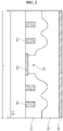
- FIGS. 1 and 2 are a plan view and a sectional view schematically showing a pixel portion of an image sensor according to a first embodiment of the present invention.
- X-ray image devices having various shapes for various purposes may be used as the X-ray image device including the image sensor 100 according to the first embodiment of the present invention.
- various X-ray image devices such as a mammography device or a CT device may be used.
- the image sensor 100 detects an X-ray passing through a subject substance and converts the X-ray into an electrical signal.
- the image sensor 100 is quadrangular in a plan view, without being limited thereto.
- the image sensor 100 is a direct-conversion type X-ray detection device, which directly converts the incident X-ray into an electrical signal.
- a plurality of pixel areas P may be disposed along row and column lines in a matrix arrangement in the image sensor 100.
- Each pixel area P may include a photoelectric conversion device that converts the X-ray into the electrical signal.
- Examples of a substrate 110 used in the image sensor 100 may include a semiconductor, for example, a silicon substrate, a glass substrate, a graphite substrate, and a substrate including an aluminum oxide (Al 2 O 3 ) base and ITO layered on the base, but are not limited thereto.
- a CMOS substrate including at least one insulating layer, a signal wire, and an electrode on a semiconductor substrate is described by way of example.
- a pixel electrode 120 and a protruding pattern 130 may be formed in the pixel area P on the substrate 110.
- the pixel electrode 120 is an electrode constituting the photoelectric conversion device and corresponds to, for example, a first electrode 120.
- the protruding pattern 130 includes the same material as the pixel electrode 120.
- the pattern is preferably formed while the pixel electrode 120 is formed, without being limited thereto.
- the pixel electrode 120 and the protruding pattern 130 may have a multilayer structure including aluminum (Al), aluminum (Al) alloy, and aluminum (Al) layers, without being limited thereto.
- a plurality of protruding patterns 130 are spaced apart from each other around the portion of the pixel area P that includes the pixel electrode 120.
- the patterns are spaced apart from the pixel electrode 120, thus being electrically insulated from the pixel electrode.
- the protruding pattern 130 may have various shapes in a plan view, for example, a dot or line shape.
- the protruding pattern 130 causes a protective film 140 formed thereon to be protruded.
- the protruding pattern 130 prefferably has a predetermined thickness so as to form the protruding protective film 140.
- the thickness of the protruding pattern 130 is particularly preferable for the thickness of the protruding pattern 130 to be the same as or larger than that of the pixel electrode 120.
- the pixel electrode 120 may have a thickness of about 0.1 ⁇ m
- the protruding pattern 130 may have a thickness that is 1.0 to 10 ⁇ m larger than that of the pixel electrode 120.
- the thickness of the protruding pattern 130 is lower than 1.0 ⁇ m, it is difficult to improve the strength of adhesion to the desired level, and when the thickness is larger than 10 ⁇ m, step coverage becomes poor due to steps.
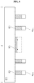
- the method of forming the pixel electrode 120 and the protruding pattern 130, which is thicker than the pixel electrode, is shown in FIGS. 3 to 6 .
- a metal material layer 111 is formed on the substrate 110, and a photoresist layer 115 is formed thereon.
- a photomask 190 having a semi-transmissive area (STA), such as a halftone mask or a diffraction exposing mask is positioned on the substrate 110 to perform an exposure process.
- STA semi-transmissive area
- a positive-type photoresist layer from which a portion receiving light is removed, is used as the photoresist layer 115.
- the photomask 190 may include the semi-transmissive area (STA), a blocking area (BA), and a transmissive area (TA), and may be disposed so that the semi-transmissive area (STA) corresponds to a portion in which the pixel electrode 120 is to be formed, the blocking area (BA) corresponds to a portion in which the protruding pattern 130 is to be formed, and the transmissive area (TA) corresponds to the remaining portion.
- STA semi-transmissive area
- BA blocking area
- TA transmissive area
- the exposure process is performed and the photoresist layer 115 is developed, depending on the disposal, thus forming first and second photoresist patterns 115a and 115b having different thicknesses, as in FIG. 4 .
- the first photoresist pattern 115a is thicker than the second photoresist pattern 115b.
- the metal material layer 111 is subjected to a first etching process using the first and second photoresist patterns 115a and 115b as etching masks, thus forming first and second metal patterns 111a and 111b beneath the first and second photoresist patterns 115a and 115b, respectively.
- the first metal pattern 111a corresponds to the protruding pattern 130.
- an ashing process is performed over the first and second photoresist patterns 115a and 115b to remove the second photoresist pattern 115b, thereby exposing the second metal pattern 111b.
- the first photoresist pattern 115a is partially removed to a predetermined thickness and a portion thereof remains on the first metal pattern 111a, that is, the protruding pattern 130.
- a second etching process is performed to partially etch the second metal pattern 111b to a predetermined thickness, thereby forming the pixel electrode 120.
- the pixel electrode 120 and the protruding pattern 130 which is thicker than the pixel electrode may be formed through one photomask process according to the aforementioned procedure.
- a protective film 140 is formed on the protruding pattern 130 and the pixel electrode 120.
- a pad hole 141 is formed in the protective film 140 to expose the pixel electrode 120 therethrough.
- the protective film 140 may be formed using an inorganic insulating material or an organic insulating material.
- the protective film 140 according to the embodiment of the present invention has a surface that is protruded due to the protruding pattern 130 formed thereunder.
- a convex portion that protrudes upwards is formed in the area including the protruding pattern 130.
- a concave portion that is indented downwards is formed in the area in which the protruding pattern 130 is not formed, that is, the area between the protruding patterns 130. Thereby, the surface of the protective film 140 is made protruded.
- the surface of the protective film 140 is protruded to thus increase the surface area thereof.
- the surface area of the protective film 140 may be increased to thus increase the contact area with a photoconductive layer 150 formed on the protective film 140 so that the strength of adhesion of the photoconductive layer 150 to the substrate can be improved.
- the protective film 140 having the protruded surface preferably has a surface area that is at least two times that of the protective film having the flat surface, without being limited thereto.
- the protective film 140 may have a monolayer structure, without being limited thereto.
- the protective film 140 may have a multilayer structure.
- a protective film 140 having a double-layer structure is shown in FIG. 7 .
- the protective film 140 may include a first protective layer 140a at a lower part and a second protective layer 140b at an upper part.
- the first protective layer 140a includes a soft material, for example, silicon oxide (SiO 2 )
- the second protective layer 140b includes a hard material, for example, silicon nitride (Si 3 N 4 ), without being limited thereto.
- the concave and convex portions are not gently formed due to the hard material, and accordingly, defects such as cracks or pinholes may be formed, resulting in current leakage.
- the first protective layer 140a includes a lower part that may be a silicon oxide layer which is rather soft. Therefore, the first protective layer 140a may be protruded, and the second protective layer 140b, which includes silicon nitride and which is formed on the first protective layer, may be influenced by the protruded form of the first protective layer 140a. Thereby, the occurrence of defects in the second protective layer 140b may be minimized. Even though the defects are occurred in the second protective layer 140b, problems like current leakage caused by the defects may be prevented by the first protective layer 140a which is formed under the seconde protective layer 140b.
- the photoconductive layer 150 is formed on the protective film 140.
- the photoconductive layer 150 generates an electron-hole pair when an X-ray is incident thereon.
- a material having an excellent charge-moving ability, a high absorption coefficient, low dark current, and low electron-hole pair generation energy may be used in the photoconductive layer 150.
- the photoconductive material groups such as CdTe, CdZnTe, PbO, PbI 2 , HgI 2 , GaAs, Se, TlBr, BiI 3 , CdMnTe, CdMg, Te, and InI, may be used.
- the photoconductive layer 150 may have a thickness of 200 to 500 ⁇ m.
- An upper electrode 160 is formed on the substantially entire surface of the substrate 110 on which the photoconductive layer 150 is formed. A bias voltage may be applied to the upper electrode 160.
- the upper electrode 160 is another electrode constituting the photoelectric conversion device, for example, a second electrode 160.
- the second electrode 160 may include, for example, Au, without being limited thereto.
- the protruding pattern 130 causes the protective film 140 to be protruded, and may concentrate an electric field between the first and second electrodes 120 and 160 to thus reduce a leakage current.
- the protruding pattern 130 is formed around the first electrode 120, thus inwardly diverting the electric field generated between the second electrode 160 and the first electrode 120.
- the protruding pattern 130 serves as a guard ring with respect to the generation of the electric field.
- the protruding pattern 130 may receive a voltage having a polarity opposite to that of the pixel electrode 120, or may be in a floating state.
- FIG. 8 is a sectional view schematically showing a pixel portion of an image sensor according to a second embodiment of the present invention.
- parts that are the same as or similar to those of the first embodiment may be omitted.
- an image sensor 100 may include a pixel electrode 120 formed on a substrate 110 and a protruding pattern 130 formed around the pixel electrode 120, a protective film 140 formed on them, a metal pattern 170 formed on the protective film 140, a photoconductive layer 150 formed on the metal pattern 170 to come into contact with the pixel electrode 120, and an upper electrode 160 formed on the photoconductive layer 150.
- the pixel electrode 120 and the protruding pattern 130 may be formed using the same process as the first embodiment, and may have a multilayer structure.
- the pixel electrode 120 and the protruding pattern 130 are exemplified as having a double-layer structure.
- first layers 120a and 130a which are lower layers of the pixel electrode 120 and the protruding pattern 130, may include aluminum (Al), and second layers 120b and 130b, which are upper layers, may include titanium (Ti), without being limited thereto.
- the pattern may have a predetermined thickness, which is required in order to form the protruded pattern due to the multilayer structure.
- the pixel electrode 120 and the protruding pattern 130 may be the same thickness.
- a photomask may not be imparted with a semi-transmissive area during an exposure process.
- the pixel electrode 120 may be partially etched using the photomask having the semi-transmissive area, as in the first embodiment, so that the pixel electrode 120 is thinner than the protruding pattern 130.
- the second layer 120b which is the upper layer, may be removed so that the pixel electrode 120 has a monolayer structure.
- the protective film 140 may have a monolayer or multilayer structure. In the present embodiment, the protective film 140 has a double-layer structure. The protective film 140 may be slightly protruded, and may have improved reliability due to the double-layer structure thereof, as in the first embodiment.
- the metal pattern 170 may be formed on the protective film 140.
- the metal pattern 170 is made protruded due to the protective film 140 positioned thereunder.
- the metal pattern 170 may include a metal material having conductivity, and particularly at least one material of gold (Au), silver (Ag), platinum (Pt), palladium (Pd), chromium (Cr), copper (Cu), titanium (Ti), and nickel (Ni).
- the metal pattern 170 may have a monolayer or multilayer structure.
- the metal pattern 170 has a double-layer structure.
- a first metal layer 170a which is a lower layer
- a second metal layer 170b which is an upper layer
- the material constituting the metal pattern 170 has excellent strength of adhesion to the protective film 140. Therefore, the metal pattern 170 may be provided between the protective film 140 and the photoconductive layer 150 formed during a subsequent process, thereby improving the strength of adhesion of the photoconductive layer 150 to the substrate 110.
- the photoconductive layer 150 has poor strength of adhesion to the protective layer 140b including silicon nitride, but the metal pattern 170 may serve to effectively improve the strength of adhesion.
- the metal pattern 170 may be spaced apart from the pixel electrode 120 so as to be electrically disconnected from the pixel electrode. That is, the metal pattern 170 may be formed in at least a portion of the surrounding area of the pixel electrode 120 in a plan view. The metal pattern 170 may have an area of about 10 to 90% of the total area of the pixel area P.
- the photoconductive layer 150 may be formed on the metal pattern 170 having the aforementioned constitution, thereby improving the strength of adhesion of the photoconductive layer 150.
- the area of the metal pattern 170 in the pixel area P may be in inverse proportion to the area of the pixel electrode 120.
- the metal pattern 170 may concentrate an electric field, like the protruding pattern of the first embodiment, thereby reducing leakage current.
- the metal pattern 170 may be formed around the pixel electrode 120, thus inwardly diverting the electric field generated between the upper electrode 160 and the pixel electrode 120.
- the metal pattern 170 may serve as a guard ring with respect to the generation of the electric field.
- the metal pattern 170 may receive a voltage having a polarity opposite to that of the pixel electrode 120, or may be in a floating state.
- the protruding pattern 130 serves as the guard ring, and both the metal pattern 170 and the protruding pattern 130 serve as the guard ring.
- a protruding pattern is formed on a substrate so that a protective film on the pattern is also formed so as to be protruded. Therefore, the contact area between a photoconductive layer, which is formed on the protective film, and the substrate, on which the protective film is formed, may be increased, thus improving the strength of adhesion of the photoconductive layer.
- the protruding pattern may be formed while the pixel electrode is formed. Accordingly, there is a merit in that process efficiency is improved compared to the case where a separate process such as surface treatment is required to make the protective film protruded.
Landscapes
- Solid State Image Pick-Up Elements (AREA)
- Health & Medical Sciences (AREA)
- Toxicology (AREA)
Claims (12)
- Bildsensor (100), aufweisend:eine erste Elektrode (120), die auf einem Substrat (110) ausgebildet ist;ein vorstehendes Muster (130), das um die erste Elektrode auf dem Substrat (110) ausgebildet ist;ein Schutzfilm, der auf dem vorstehenden Muster (130) ausgebildet ist, um eine vorstehende Oberfläche zu haben, die von dem vorstehenden Muster (130) gebildet wird, und um eine Pad-Öffnung zu haben, die die erste Elektrode freilegt;eine fotoleitende Schicht (150), die auf dem Schutzfilm ausgebildet ist und die erste Elektrode durch die Pad-Öffnung hindurch kontaktiert; undeine zweite Elektrode (160), die auf der fotoleitenden Schicht (150) ausgebildet ist,dadurch gekennzeichnet, dassdas vorstehende Muster (130) einen Schutzring zum Umleiten eines elektrischen Felds zwischen der ersten Elektrode und der zweiten Elektrode umfasst.
- Bildsensor (100) nach Anspruch 1, wobei das vorstehende Muster (130) und die erste Elektrode durch ein gleiches Material und auf einer gleichen Schicht gebildet sind.
- Bildsensor (100) nach Anspruch 1, wobei eine Dicke des vorstehenden Musters (130) größer oder gleich einer Dicke der ersten Elektrode ist.
- Bildsensor (100) nach Anspruch 1, wobei ein Oberflächenbereich des Schutzfilms gleich oder mehr als zweimal einem flachen Oberflächenbereich des Schutzfilms ist.
- Bildsensor (100) nach Anspruch 1, wobei das vorstehende Muster (130) eine Spannung erhält oder in einem schwimmenden Zustand ist.
- Bildsensor (100) nach Anspruch 1, wobei der Bildsensor (100) ferner aufweist:
ein Metallmuster (170), das zwischen dem Schutzfilm und der fotoleitenden Schicht (150) ausgebildet ist, das eine ganze Schicht oder Mehrschichtstruktur hat, und das eine Spannung erhält oder in einem schwimmenden Zustand ist. - Bildsensor (100) nach Anspruch 6, wobei das Metallmuster (170) wenigstens eines der nachfolgenden Materialien enthält: Au, Pt, Pd, Cr, Cu, Ti, oder Ni.
- Bildsensor (100) des Anspruchs 1, wobei der Schutzfilm eine erste Schutzschicht umfasst, die Silikonoxide umfasst, und eine zweite Schutzschicht, die Silikonnitride auf der ersten Schutzschicht umfasst.
- Bildsensor (100) des Anspruchs 1, wobei die erste Elektrode und das vorstehende Muster (130) eine Vielschichtstruktur haben.
- Bildsensor (100) des Anspruchs 1, wobei die fotoleitende Schicht (150) wenigstens eines der nachfolgenden Materialien umfasst: CdTe, CdZnTe, PbO, Pbl2, Hgl2, GaAs, Se, TIBr, Bil3, CdMnTe, CdMg, Te, oder Inl.
- Bildsensor (100) des Anspruchs 1, wobei eine Dicke des vorstehenden Musters (130) zwischen 1,0 µm und 10,0 µm liegt.
- Bildsensor (100) des Anspruchs 1, wobei der Schutzfilm wenigstens zwei Schichten mit unterschiedlicher Härte umfasst.
Applications Claiming Priority (2)
| Application Number | Priority Date | Filing Date | Title |
|---|---|---|---|
| KR1020140041196A KR102263382B1 (ko) | 2014-04-07 | 2014-04-07 | 이미지센서 및 이의 제조방법 |
| PCT/KR2015/003447 WO2015156567A1 (ko) | 2014-04-07 | 2015-04-07 | 이미지센서 및 이의 제조방법 |
Publications (3)
| Publication Number | Publication Date |
|---|---|
| EP3128554A1 EP3128554A1 (de) | 2017-02-08 |
| EP3128554A4 EP3128554A4 (de) | 2017-11-22 |
| EP3128554B1 true EP3128554B1 (de) | 2019-11-27 |
Family
ID=54288085
Family Applications (1)
| Application Number | Title | Priority Date | Filing Date |
|---|---|---|---|
| EP15776781.5A Active EP3128554B1 (de) | 2014-04-07 | 2015-04-07 | Bildsensor |
Country Status (4)
| Country | Link |
|---|---|
| US (1) | US9923018B2 (de) |
| EP (1) | EP3128554B1 (de) |
| KR (1) | KR102263382B1 (de) |
| WO (1) | WO2015156567A1 (de) |
Family Cites Families (12)
| Publication number | Priority date | Publication date | Assignee | Title |
|---|---|---|---|---|
| US4621275A (en) * | 1983-04-30 | 1986-11-04 | Matsushita Electric Industrial Co., Ltd. | Solid-state imaging device |
| JPH06260625A (ja) * | 1993-03-09 | 1994-09-16 | Seiko Instr Inc | イメージセンサ装置及び製造方法 |
| US6025599A (en) * | 1997-12-09 | 2000-02-15 | Direct Radiography Corp. | Image capture element |
| DE19825450A1 (de) * | 1998-06-06 | 1999-12-09 | Philips Patentverwaltung | Röntgenbildsensor |
| US6891194B2 (en) | 2001-02-07 | 2005-05-10 | Sharp Kabushiki Kaisha | Active matrix substrate, electromagnetic detector, and liquid crystal display apparatus |
| FR2833410B1 (fr) * | 2001-12-10 | 2004-03-19 | Commissariat Energie Atomique | Procede de realisation d'un dispositif d'imagerie |
| KR100551569B1 (ko) * | 2003-11-04 | 2006-02-13 | 남상희 | 플라즈마 디스플레이 패널 구조를 이용한 디지털 엑스레이 검출기판 |
| KR100718881B1 (ko) | 2005-12-28 | 2007-05-17 | (주)실리콘화일 | 이미지센서용 포토다이오드 및 그 제조 방법 |
| JP5280671B2 (ja) * | 2006-12-20 | 2013-09-04 | 富士フイルム株式会社 | 画像検出器および放射線検出システム |
| US7671385B2 (en) * | 2007-03-15 | 2010-03-02 | Powerchip Semiconductor Corp. | Image sensor and fabrication method thereof |
| KR100850289B1 (ko) * | 2007-06-08 | 2008-08-04 | (주)실리콘화일 | 적층 구조의 이미지센서 및 그 제조방법 |
| JP2010206128A (ja) * | 2009-03-06 | 2010-09-16 | Seiko Epson Corp | 光電変換素子、光電変換装置、及びイメージセンサ |
-
2014
- 2014-04-07 KR KR1020140041196A patent/KR102263382B1/ko active Active
-
2015
- 2015-04-07 WO PCT/KR2015/003447 patent/WO2015156567A1/ko not_active Ceased
- 2015-04-07 EP EP15776781.5A patent/EP3128554B1/de active Active
- 2015-04-07 US US15/302,251 patent/US9923018B2/en active Active
Non-Patent Citations (1)
| Title |
|---|
| None * |
Also Published As
| Publication number | Publication date |
|---|---|
| WO2015156567A1 (ko) | 2015-10-15 |
| KR20150116230A (ko) | 2015-10-15 |
| EP3128554A4 (de) | 2017-11-22 |
| KR102263382B1 (ko) | 2021-06-11 |
| US9923018B2 (en) | 2018-03-20 |
| US20170033149A1 (en) | 2017-02-02 |
| EP3128554A1 (de) | 2017-02-08 |
Similar Documents
| Publication | Publication Date | Title |
|---|---|---|
| JP6099035B2 (ja) | 光電変換装置及びその製造方法並びにx線画像検出装置 | |
| US8614423B2 (en) | Solid-state radiation detector with improved sensitivity | |
| JP2009527922A (ja) | ダイレクトフォトリソグラフィーを用いた、放射線検出器のためのセグメント化接触子の製造方法 | |
| JP6125017B2 (ja) | X線イメージセンサー用基板 | |
| KR101218089B1 (ko) | 디지털 엑스레이 디텍터 및 그 제조방법 | |
| KR20200133797A (ko) | 방사선 검출 소자, 및 그의 제조 방법 | |
| KR101941426B1 (ko) | 이미지센서 및 그 제조방법 | |
| KR20190037629A (ko) | 광 검출 장치 및 그의 제조 방법 | |
| US7767487B2 (en) | Formation of contacts on semiconductor substrates | |
| KR102195521B1 (ko) | 엑스레이 검출기의 어레이 기판 및 그의 제조 방법 | |
| EP3128554B1 (de) | Bildsensor | |
| KR101686676B1 (ko) | 엑스레이 검출기의 어레이 기판 및 그 제조방법 | |
| KR102129261B1 (ko) | 엑스레이 검출기의 어레이 기판 및 그의 제조 방법 | |
| KR20110062163A (ko) | 엑스레이 검출기 | |
| KR20150067808A (ko) | 엑스레이 검출기의 어레이 기판 및 그의 제조 방법 | |
| US20160155770A1 (en) | Image sensor and method for manufacturing same | |
| KR102280924B1 (ko) | 이미지센서 및 그 제조방법 | |
| KR102813182B1 (ko) | 디지털 엑스레이 검출기용 어레이 기판과 이를 포함하는 디지털 엑스레이 검출기 및 그 제조 방법 | |
| KR20190028195A (ko) | 엑스레이 검출기용 어레이 기판과 이를 포함하는 엑스레이 검출기 및 그 제조 방법 | |
| KR101486250B1 (ko) | 이미지센서와 그 제조방법 | |
| KR102123849B1 (ko) | 엑스레이 검출기의 어레이 기판 및 그의 제조 방법 | |
| KR20160111671A (ko) | 이미지센서 및 이의 제조방법 | |
| KR20160080076A (ko) | 이미지센서 및 그 제조방법 | |
| JP4835838B2 (ja) | 二次元画像検出器の製造方法 | |
| CN116646365A (zh) | 图像传感器及其制作方法 |
Legal Events
| Date | Code | Title | Description |
|---|---|---|---|
| STAA | Information on the status of an ep patent application or granted ep patent |
Free format text: STATUS: THE INTERNATIONAL PUBLICATION HAS BEEN MADE |
|
| PUAI | Public reference made under article 153(3) epc to a published international application that has entered the european phase |
Free format text: ORIGINAL CODE: 0009012 |
|
| STAA | Information on the status of an ep patent application or granted ep patent |
Free format text: STATUS: REQUEST FOR EXAMINATION WAS MADE |
|
| 17P | Request for examination filed |
Effective date: 20161102 |
|
| AK | Designated contracting states |
Kind code of ref document: A1 Designated state(s): AL AT BE BG CH CY CZ DE DK EE ES FI FR GB GR HR HU IE IS IT LI LT LU LV MC MK MT NL NO PL PT RO RS SE SI SK SM TR |
|
| AX | Request for extension of the european patent |
Extension state: BA ME |
|
| DAV | Request for validation of the european patent (deleted) | ||
| DAX | Request for extension of the european patent (deleted) | ||
| A4 | Supplementary search report drawn up and despatched |
Effective date: 20171019 |
|
| RIC1 | Information provided on ipc code assigned before grant |
Ipc: H01L 27/146 20060101AFI20171013BHEP |
|
| GRAP | Despatch of communication of intention to grant a patent |
Free format text: ORIGINAL CODE: EPIDOSNIGR1 |
|
| STAA | Information on the status of an ep patent application or granted ep patent |
Free format text: STATUS: GRANT OF PATENT IS INTENDED |
|
| INTG | Intention to grant announced |
Effective date: 20190717 |
|
| GRAS | Grant fee paid |
Free format text: ORIGINAL CODE: EPIDOSNIGR3 |
|
| GRAA | (expected) grant |
Free format text: ORIGINAL CODE: 0009210 |
|
| STAA | Information on the status of an ep patent application or granted ep patent |
Free format text: STATUS: THE PATENT HAS BEEN GRANTED |
|
| AK | Designated contracting states |
Kind code of ref document: B1 Designated state(s): AL AT BE BG CH CY CZ DE DK EE ES FI FR GB GR HR HU IE IS IT LI LT LU LV MC MK MT NL NO PL PT RO RS SE SI SK SM TR |
|
| REG | Reference to a national code |
Ref country code: GB Ref legal event code: FG4D |
|
| REG | Reference to a national code |
Ref country code: CH Ref legal event code: EP |
|
| REG | Reference to a national code |
Ref country code: AT Ref legal event code: REF Ref document number: 1207673 Country of ref document: AT Kind code of ref document: T Effective date: 20191215 |
|
| REG | Reference to a national code |
Ref country code: DE Ref legal event code: R096 Ref document number: 602015042576 Country of ref document: DE |
|
| REG | Reference to a national code |
Ref country code: IE Ref legal event code: FG4D |
|
| REG | Reference to a national code |
Ref country code: NL Ref legal event code: MP Effective date: 20191127 |
|
| REG | Reference to a national code |
Ref country code: LT Ref legal event code: MG4D |
|
| PG25 | Lapsed in a contracting state [announced via postgrant information from national office to epo] |
Ref country code: GR Free format text: LAPSE BECAUSE OF FAILURE TO SUBMIT A TRANSLATION OF THE DESCRIPTION OR TO PAY THE FEE WITHIN THE PRESCRIBED TIME-LIMIT Effective date: 20200228 Ref country code: BG Free format text: LAPSE BECAUSE OF FAILURE TO SUBMIT A TRANSLATION OF THE DESCRIPTION OR TO PAY THE FEE WITHIN THE PRESCRIBED TIME-LIMIT Effective date: 20200227 Ref country code: FI Free format text: LAPSE BECAUSE OF FAILURE TO SUBMIT A TRANSLATION OF THE DESCRIPTION OR TO PAY THE FEE WITHIN THE PRESCRIBED TIME-LIMIT Effective date: 20191127 Ref country code: NO Free format text: LAPSE BECAUSE OF FAILURE TO SUBMIT A TRANSLATION OF THE DESCRIPTION OR TO PAY THE FEE WITHIN THE PRESCRIBED TIME-LIMIT Effective date: 20200227 Ref country code: LT Free format text: LAPSE BECAUSE OF FAILURE TO SUBMIT A TRANSLATION OF THE DESCRIPTION OR TO PAY THE FEE WITHIN THE PRESCRIBED TIME-LIMIT Effective date: 20191127 Ref country code: NL Free format text: LAPSE BECAUSE OF FAILURE TO SUBMIT A TRANSLATION OF THE DESCRIPTION OR TO PAY THE FEE WITHIN THE PRESCRIBED TIME-LIMIT Effective date: 20191127 Ref country code: SE Free format text: LAPSE BECAUSE OF FAILURE TO SUBMIT A TRANSLATION OF THE DESCRIPTION OR TO PAY THE FEE WITHIN THE PRESCRIBED TIME-LIMIT Effective date: 20191127 Ref country code: LV Free format text: LAPSE BECAUSE OF FAILURE TO SUBMIT A TRANSLATION OF THE DESCRIPTION OR TO PAY THE FEE WITHIN THE PRESCRIBED TIME-LIMIT Effective date: 20191127 |
|
| PG25 | Lapsed in a contracting state [announced via postgrant information from national office to epo] |
Ref country code: HR Free format text: LAPSE BECAUSE OF FAILURE TO SUBMIT A TRANSLATION OF THE DESCRIPTION OR TO PAY THE FEE WITHIN THE PRESCRIBED TIME-LIMIT Effective date: 20191127 Ref country code: IS Free format text: LAPSE BECAUSE OF FAILURE TO SUBMIT A TRANSLATION OF THE DESCRIPTION OR TO PAY THE FEE WITHIN THE PRESCRIBED TIME-LIMIT Effective date: 20200327 Ref country code: RS Free format text: LAPSE BECAUSE OF FAILURE TO SUBMIT A TRANSLATION OF THE DESCRIPTION OR TO PAY THE FEE WITHIN THE PRESCRIBED TIME-LIMIT Effective date: 20191127 |
|
| PG25 | Lapsed in a contracting state [announced via postgrant information from national office to epo] |
Ref country code: AL Free format text: LAPSE BECAUSE OF FAILURE TO SUBMIT A TRANSLATION OF THE DESCRIPTION OR TO PAY THE FEE WITHIN THE PRESCRIBED TIME-LIMIT Effective date: 20191127 |
|
| PG25 | Lapsed in a contracting state [announced via postgrant information from national office to epo] |
Ref country code: RO Free format text: LAPSE BECAUSE OF FAILURE TO SUBMIT A TRANSLATION OF THE DESCRIPTION OR TO PAY THE FEE WITHIN THE PRESCRIBED TIME-LIMIT Effective date: 20191127 Ref country code: CZ Free format text: LAPSE BECAUSE OF FAILURE TO SUBMIT A TRANSLATION OF THE DESCRIPTION OR TO PAY THE FEE WITHIN THE PRESCRIBED TIME-LIMIT Effective date: 20191127 Ref country code: DK Free format text: LAPSE BECAUSE OF FAILURE TO SUBMIT A TRANSLATION OF THE DESCRIPTION OR TO PAY THE FEE WITHIN THE PRESCRIBED TIME-LIMIT Effective date: 20191127 Ref country code: PT Free format text: LAPSE BECAUSE OF FAILURE TO SUBMIT A TRANSLATION OF THE DESCRIPTION OR TO PAY THE FEE WITHIN THE PRESCRIBED TIME-LIMIT Effective date: 20200419 Ref country code: EE Free format text: LAPSE BECAUSE OF FAILURE TO SUBMIT A TRANSLATION OF THE DESCRIPTION OR TO PAY THE FEE WITHIN THE PRESCRIBED TIME-LIMIT Effective date: 20191127 Ref country code: ES Free format text: LAPSE BECAUSE OF FAILURE TO SUBMIT A TRANSLATION OF THE DESCRIPTION OR TO PAY THE FEE WITHIN THE PRESCRIBED TIME-LIMIT Effective date: 20191127 |
|
| REG | Reference to a national code |
Ref country code: DE Ref legal event code: R097 Ref document number: 602015042576 Country of ref document: DE |
|
| PG25 | Lapsed in a contracting state [announced via postgrant information from national office to epo] |
Ref country code: SM Free format text: LAPSE BECAUSE OF FAILURE TO SUBMIT A TRANSLATION OF THE DESCRIPTION OR TO PAY THE FEE WITHIN THE PRESCRIBED TIME-LIMIT Effective date: 20191127 Ref country code: SK Free format text: LAPSE BECAUSE OF FAILURE TO SUBMIT A TRANSLATION OF THE DESCRIPTION OR TO PAY THE FEE WITHIN THE PRESCRIBED TIME-LIMIT Effective date: 20191127 |
|
| REG | Reference to a national code |
Ref country code: AT Ref legal event code: MK05 Ref document number: 1207673 Country of ref document: AT Kind code of ref document: T Effective date: 20191127 |
|
| PLBE | No opposition filed within time limit |
Free format text: ORIGINAL CODE: 0009261 |
|
| STAA | Information on the status of an ep patent application or granted ep patent |
Free format text: STATUS: NO OPPOSITION FILED WITHIN TIME LIMIT |
|
| 26N | No opposition filed |
Effective date: 20200828 |
|
| PG25 | Lapsed in a contracting state [announced via postgrant information from national office to epo] |
Ref country code: MC Free format text: LAPSE BECAUSE OF FAILURE TO SUBMIT A TRANSLATION OF THE DESCRIPTION OR TO PAY THE FEE WITHIN THE PRESCRIBED TIME-LIMIT Effective date: 20191127 Ref country code: PL Free format text: LAPSE BECAUSE OF FAILURE TO SUBMIT A TRANSLATION OF THE DESCRIPTION OR TO PAY THE FEE WITHIN THE PRESCRIBED TIME-LIMIT Effective date: 20191127 Ref country code: AT Free format text: LAPSE BECAUSE OF FAILURE TO SUBMIT A TRANSLATION OF THE DESCRIPTION OR TO PAY THE FEE WITHIN THE PRESCRIBED TIME-LIMIT Effective date: 20191127 Ref country code: SI Free format text: LAPSE BECAUSE OF FAILURE TO SUBMIT A TRANSLATION OF THE DESCRIPTION OR TO PAY THE FEE WITHIN THE PRESCRIBED TIME-LIMIT Effective date: 20191127 |
|
| REG | Reference to a national code |
Ref country code: CH Ref legal event code: PL |
|
| PG25 | Lapsed in a contracting state [announced via postgrant information from national office to epo] |
Ref country code: CH Free format text: LAPSE BECAUSE OF NON-PAYMENT OF DUE FEES Effective date: 20200430 Ref country code: IT Free format text: LAPSE BECAUSE OF FAILURE TO SUBMIT A TRANSLATION OF THE DESCRIPTION OR TO PAY THE FEE WITHIN THE PRESCRIBED TIME-LIMIT Effective date: 20191127 Ref country code: LU Free format text: LAPSE BECAUSE OF NON-PAYMENT OF DUE FEES Effective date: 20200407 Ref country code: LI Free format text: LAPSE BECAUSE OF NON-PAYMENT OF DUE FEES Effective date: 20200430 |
|
| REG | Reference to a national code |
Ref country code: BE Ref legal event code: MM Effective date: 20200430 |
|
| PG25 | Lapsed in a contracting state [announced via postgrant information from national office to epo] |
Ref country code: BE Free format text: LAPSE BECAUSE OF NON-PAYMENT OF DUE FEES Effective date: 20200430 |
|
| PG25 | Lapsed in a contracting state [announced via postgrant information from national office to epo] |
Ref country code: IE Free format text: LAPSE BECAUSE OF NON-PAYMENT OF DUE FEES Effective date: 20200407 |
|
| PG25 | Lapsed in a contracting state [announced via postgrant information from national office to epo] |
Ref country code: TR Free format text: LAPSE BECAUSE OF FAILURE TO SUBMIT A TRANSLATION OF THE DESCRIPTION OR TO PAY THE FEE WITHIN THE PRESCRIBED TIME-LIMIT Effective date: 20191127 Ref country code: MT Free format text: LAPSE BECAUSE OF FAILURE TO SUBMIT A TRANSLATION OF THE DESCRIPTION OR TO PAY THE FEE WITHIN THE PRESCRIBED TIME-LIMIT Effective date: 20191127 Ref country code: CY Free format text: LAPSE BECAUSE OF FAILURE TO SUBMIT A TRANSLATION OF THE DESCRIPTION OR TO PAY THE FEE WITHIN THE PRESCRIBED TIME-LIMIT Effective date: 20191127 |
|
| PG25 | Lapsed in a contracting state [announced via postgrant information from national office to epo] |
Ref country code: MK Free format text: LAPSE BECAUSE OF FAILURE TO SUBMIT A TRANSLATION OF THE DESCRIPTION OR TO PAY THE FEE WITHIN THE PRESCRIBED TIME-LIMIT Effective date: 20191127 |
|
| P01 | Opt-out of the competence of the unified patent court (upc) registered |
Effective date: 20230525 |
|
| REG | Reference to a national code |
Ref country code: DE Ref legal event code: R079 Ref document number: 602015042576 Country of ref document: DE Free format text: PREVIOUS MAIN CLASS: H01L0027146000 Ipc: H10F0039180000 |
|
| PGFP | Annual fee paid to national office [announced via postgrant information from national office to epo] |
Ref country code: DE Payment date: 20250407 Year of fee payment: 11 |
|
| PGFP | Annual fee paid to national office [announced via postgrant information from national office to epo] |
Ref country code: GB Payment date: 20260324 Year of fee payment: 12 |
|
| PGFP | Annual fee paid to national office [announced via postgrant information from national office to epo] |
Ref country code: FR Payment date: 20260323 Year of fee payment: 12 |