EP3125003A1 - Light redirecting film and display system incorporating same - Google Patents
Light redirecting film and display system incorporating same Download PDFInfo
- Publication number
- EP3125003A1 EP3125003A1 EP16183364.5A EP16183364A EP3125003A1 EP 3125003 A1 EP3125003 A1 EP 3125003A1 EP 16183364 A EP16183364 A EP 16183364A EP 3125003 A1 EP3125003 A1 EP 3125003A1
- Authority
- EP
- European Patent Office
- Prior art keywords
- film
- less
- optical
- item
- structured surface
- Prior art date
- Legal status (The legal status is an assumption and is not a legal conclusion. Google has not performed a legal analysis and makes no representation as to the accuracy of the status listed.)
- Withdrawn
Links
- 239000012788 optical film Substances 0.000 claims abstract description 184
- 230000003287 optical effect Effects 0.000 claims abstract description 173
- 239000010408 film Substances 0.000 claims description 260
- 239000002245 particle Substances 0.000 claims description 61
- 239000000758 substrate Substances 0.000 description 50
- 238000001228 spectrum Methods 0.000 description 30
- 239000000463 material Substances 0.000 description 27
- 239000010410 layer Substances 0.000 description 23
- 238000009826 distribution Methods 0.000 description 21
- 239000002105 nanoparticle Substances 0.000 description 21
- 230000005540 biological transmission Effects 0.000 description 19
- VYPSYNLAJGMNEJ-UHFFFAOYSA-N Silicium dioxide Chemical compound O=[Si]=O VYPSYNLAJGMNEJ-UHFFFAOYSA-N 0.000 description 18
- 239000000203 mixture Substances 0.000 description 18
- 238000000576 coating method Methods 0.000 description 16
- 238000000034 method Methods 0.000 description 16
- 239000011248 coating agent Substances 0.000 description 15
- 238000010276 construction Methods 0.000 description 12
- 239000000377 silicon dioxide Substances 0.000 description 8
- 230000009466 transformation Effects 0.000 description 8
- 230000007547 defect Effects 0.000 description 7
- 230000008569 process Effects 0.000 description 6
- 230000008859 change Effects 0.000 description 5
- 239000010415 colloidal nanoparticle Substances 0.000 description 5
- 230000000875 corresponding effect Effects 0.000 description 5
- 239000006185 dispersion Substances 0.000 description 5
- 229920005989 resin Polymers 0.000 description 5
- 239000011347 resin Substances 0.000 description 5
- 239000007787 solid Substances 0.000 description 5
- 239000002904 solvent Substances 0.000 description 5
- 239000011324 bead Substances 0.000 description 4
- 238000004364 calculation method Methods 0.000 description 4
- 239000004973 liquid crystal related substance Substances 0.000 description 4
- -1 polyethylene naphthalate Polymers 0.000 description 4
- 239000005020 polyethylene terephthalate Substances 0.000 description 4
- 229920000139 polyethylene terephthalate Polymers 0.000 description 4
- 229920000642 polymer Polymers 0.000 description 4
- 238000007711 solidification Methods 0.000 description 4
- 230000008023 solidification Effects 0.000 description 4
- 238000012360 testing method Methods 0.000 description 4
- 230000000295 complement effect Effects 0.000 description 3
- 230000008878 coupling Effects 0.000 description 3
- 238000010168 coupling process Methods 0.000 description 3
- 238000005859 coupling reaction Methods 0.000 description 3
- 230000001186 cumulative effect Effects 0.000 description 3
- 230000002708 enhancing effect Effects 0.000 description 3
- 239000007788 liquid Substances 0.000 description 3
- 238000004519 manufacturing process Methods 0.000 description 3
- 230000000737 periodic effect Effects 0.000 description 3
- ILJSQTXMGCGYMG-UHFFFAOYSA-N triacetic acid Chemical compound CC(=O)CC(=O)CC(O)=O ILJSQTXMGCGYMG-UHFFFAOYSA-N 0.000 description 3
- 239000004593 Epoxy Substances 0.000 description 2
- GWEVSGVZZGPLCZ-UHFFFAOYSA-N Titan oxide Chemical compound O=[Ti]=O GWEVSGVZZGPLCZ-UHFFFAOYSA-N 0.000 description 2
- MCMNRKCIXSYSNV-UHFFFAOYSA-N Zirconium dioxide Chemical compound O=[Zr]=O MCMNRKCIXSYSNV-UHFFFAOYSA-N 0.000 description 2
- 230000002411 adverse Effects 0.000 description 2
- 238000000089 atomic force micrograph Methods 0.000 description 2
- 239000011127 biaxially oriented polypropylene Substances 0.000 description 2
- 239000011230 binding agent Substances 0.000 description 2
- 230000015572 biosynthetic process Effects 0.000 description 2
- 230000003749 cleanliness Effects 0.000 description 2
- 239000011247 coating layer Substances 0.000 description 2
- 238000001723 curing Methods 0.000 description 2
- 230000000694 effects Effects 0.000 description 2
- 229910052751 metal Inorganic materials 0.000 description 2
- 239000002184 metal Substances 0.000 description 2
- 238000012986 modification Methods 0.000 description 2
- 230000004048 modification Effects 0.000 description 2
- 239000000178 monomer Substances 0.000 description 2
- 230000010363 phase shift Effects 0.000 description 2
- 229920000515 polycarbonate Polymers 0.000 description 2
- 239000004417 polycarbonate Substances 0.000 description 2
- OKTJSMMVPCPJKN-UHFFFAOYSA-N Carbon Chemical compound [C] OKTJSMMVPCPJKN-UHFFFAOYSA-N 0.000 description 1
- 239000004971 Cross linker Substances 0.000 description 1
- 239000004952 Polyamide Substances 0.000 description 1
- 239000004642 Polyimide Substances 0.000 description 1
- 239000004793 Polystyrene Substances 0.000 description 1
- BQCADISMDOOEFD-UHFFFAOYSA-N Silver Chemical compound [Ag] BQCADISMDOOEFD-UHFFFAOYSA-N 0.000 description 1
- 239000004809 Teflon Substances 0.000 description 1
- 229920006362 Teflon® Polymers 0.000 description 1
- 238000003848 UV Light-Curing Methods 0.000 description 1
- 239000011149 active material Substances 0.000 description 1
- PNEYBMLMFCGWSK-UHFFFAOYSA-N aluminium oxide Inorganic materials [O-2].[O-2].[O-2].[Al+3].[Al+3] PNEYBMLMFCGWSK-UHFFFAOYSA-N 0.000 description 1
- 229910000410 antimony oxide Inorganic materials 0.000 description 1
- 229920006378 biaxially oriented polypropylene Polymers 0.000 description 1
- 229920002301 cellulose acetate Polymers 0.000 description 1
- 239000003795 chemical substances by application Substances 0.000 description 1
- 239000002131 composite material Substances 0.000 description 1
- 150000001875 compounds Chemical class 0.000 description 1
- 238000001816 cooling Methods 0.000 description 1
- 230000002596 correlated effect Effects 0.000 description 1
- 239000002537 cosmetic Substances 0.000 description 1
- 238000004132 cross linking Methods 0.000 description 1
- 238000004070 electrodeposition Methods 0.000 description 1
- 238000001227 electron beam curing Methods 0.000 description 1
- 238000004049 embossing Methods 0.000 description 1
- 125000003700 epoxy group Chemical group 0.000 description 1
- 239000011888 foil Substances 0.000 description 1
- 229910021485 fumed silica Inorganic materials 0.000 description 1
- 239000011521 glass Substances 0.000 description 1
- 238000007756 gravure coating Methods 0.000 description 1
- 238000005286 illumination Methods 0.000 description 1
- 239000003999 initiator Substances 0.000 description 1
- 230000000873 masking effect Effects 0.000 description 1
- 238000005259 measurement Methods 0.000 description 1
- 229910044991 metal oxide Inorganic materials 0.000 description 1
- 150000004706 metal oxides Chemical class 0.000 description 1
- 238000001000 micrograph Methods 0.000 description 1
- 230000000116 mitigating effect Effects 0.000 description 1
- 239000004745 nonwoven fabric Substances 0.000 description 1
- 239000013307 optical fiber Substances 0.000 description 1
- VTRUBDSFZJNXHI-UHFFFAOYSA-N oxoantimony Chemical compound [Sb]=O VTRUBDSFZJNXHI-UHFFFAOYSA-N 0.000 description 1
- 229920001568 phenolic resin Polymers 0.000 description 1
- 239000005011 phenolic resin Substances 0.000 description 1
- 230000000704 physical effect Effects 0.000 description 1
- 229920003207 poly(ethylene-2,6-naphthalate) Polymers 0.000 description 1
- 229920003229 poly(methyl methacrylate) Polymers 0.000 description 1
- 229920002285 poly(styrene-co-acrylonitrile) Polymers 0.000 description 1
- 229920002647 polyamide Polymers 0.000 description 1
- 229920000647 polyepoxide Polymers 0.000 description 1
- 229920006267 polyester film Polymers 0.000 description 1
- 239000011112 polyethylene naphthalate Substances 0.000 description 1
- 229920001721 polyimide Polymers 0.000 description 1
- 239000002952 polymeric resin Substances 0.000 description 1
- 239000004926 polymethyl methacrylate Substances 0.000 description 1
- 229920000098 polyolefin Polymers 0.000 description 1
- 229920002223 polystyrene Polymers 0.000 description 1
- 230000009257 reactivity Effects 0.000 description 1
- 238000004064 recycling Methods 0.000 description 1
- 230000009467 reduction Effects 0.000 description 1
- 238000011160 research Methods 0.000 description 1
- 238000005096 rolling process Methods 0.000 description 1
- 238000001878 scanning electron micrograph Methods 0.000 description 1
- 238000006748 scratching Methods 0.000 description 1
- 230000002393 scratching effect Effects 0.000 description 1
- 238000007493 shaping process Methods 0.000 description 1
- 229910052709 silver Inorganic materials 0.000 description 1
- 239000004332 silver Substances 0.000 description 1
- 239000002356 single layer Substances 0.000 description 1
- 238000004381 surface treatment Methods 0.000 description 1
- 239000012756 surface treatment agent Substances 0.000 description 1
- 229920003002 synthetic resin Polymers 0.000 description 1
- 238000001029 thermal curing Methods 0.000 description 1
- 230000008719 thickening Effects 0.000 description 1
- XOLBLPGZBRYERU-UHFFFAOYSA-N tin dioxide Chemical compound O=[Sn]=O XOLBLPGZBRYERU-UHFFFAOYSA-N 0.000 description 1
- 229910001887 tin oxide Inorganic materials 0.000 description 1
- 238000012876 topography Methods 0.000 description 1
- 238000004627 transmission electron microscopy Methods 0.000 description 1
- 238000012800 visualization Methods 0.000 description 1
- 238000010792 warming Methods 0.000 description 1
Images


Classifications
-
- G—PHYSICS
- G02—OPTICS
- G02B—OPTICAL ELEMENTS, SYSTEMS OR APPARATUS
- G02B5/00—Optical elements other than lenses
- G02B5/04—Prisms
-
- G—PHYSICS
- G02—OPTICS
- G02B—OPTICAL ELEMENTS, SYSTEMS OR APPARATUS
- G02B5/00—Optical elements other than lenses
- G02B5/02—Diffusing elements; Afocal elements
- G02B5/0205—Diffusing elements; Afocal elements characterised by the diffusing properties
- G02B5/021—Diffusing elements; Afocal elements characterised by the diffusing properties the diffusion taking place at the element's surface, e.g. by means of surface roughening or microprismatic structures
- G02B5/0221—Diffusing elements; Afocal elements characterised by the diffusing properties the diffusion taking place at the element's surface, e.g. by means of surface roughening or microprismatic structures the surface having an irregular structure
-
- G—PHYSICS
- G02—OPTICS
- G02B—OPTICAL ELEMENTS, SYSTEMS OR APPARATUS
- G02B1/00—Optical elements characterised by the material of which they are made; Optical coatings for optical elements
- G02B1/10—Optical coatings produced by application to, or surface treatment of, optical elements
-
- G—PHYSICS
- G02—OPTICS
- G02B—OPTICAL ELEMENTS, SYSTEMS OR APPARATUS
- G02B5/00—Optical elements other than lenses
-
- G—PHYSICS
- G02—OPTICS
- G02B—OPTICAL ELEMENTS, SYSTEMS OR APPARATUS
- G02B5/00—Optical elements other than lenses
- G02B5/02—Diffusing elements; Afocal elements
- G02B5/0205—Diffusing elements; Afocal elements characterised by the diffusing properties
- G02B5/0236—Diffusing elements; Afocal elements characterised by the diffusing properties the diffusion taking place within the volume of the element
- G02B5/0242—Diffusing elements; Afocal elements characterised by the diffusing properties the diffusion taking place within the volume of the element by means of dispersed particles
-
- G—PHYSICS
- G02—OPTICS
- G02B—OPTICAL ELEMENTS, SYSTEMS OR APPARATUS
- G02B5/00—Optical elements other than lenses
- G02B5/02—Diffusing elements; Afocal elements
- G02B5/0268—Diffusing elements; Afocal elements characterized by the fabrication or manufacturing method
-
- G—PHYSICS
- G02—OPTICS
- G02B—OPTICAL ELEMENTS, SYSTEMS OR APPARATUS
- G02B5/00—Optical elements other than lenses
- G02B5/02—Diffusing elements; Afocal elements
- G02B5/0273—Diffusing elements; Afocal elements characterized by the use
- G02B5/0278—Diffusing elements; Afocal elements characterized by the use used in transmission
Definitions
- This description generally relates to optical film for redirecting light. This description is further applicable to optical systems, such as display systems, incorporating such optical films.
- Display systems such as liquid crystal display (LCD) systems, are used in a variety of applications and commercially available devices such as, for example, computer monitors, personal digital assistants (PDAs), mobile phones, miniature music players, and thin LCD televisions.
- LCDs include a liquid crystal panel and an extended area light source, often referred to as a backlight, for illuminating the liquid crystal panel.
- Backlights typically include one or more lamps and a number of light management films such as, for example, lightguides, mirror films, light redirecting films, retarder films, light polarizing films, and diffuser films.
- Diffuser films are typically included to hide optical defects and improve the brightness uniformity of the light emitted by the backlight.
- the present description relates to an optical film that has a structured surface.
- the optical film has an optical haze of less than about 10% and an optical clarity of less than about 50%.
- At least 85% of the structured surface of the film has a slope magnitude that is less than about 7.5 degrees.
- the present invention relates to an optical film that has a structured surface.
- the optical film has an optical haze of less than about 7.5% and an optical clarity of less than about 60%.
- At least 90% of the structured surface of the film has a slope magnitude that is less than about 7.5 degrees.
- the film also is made up in part of a plurality of particles having an average size that is less than about 0.5 microns.
- the present description relates to an optical film that has a structured surface.
- the optical film has an optical haze of less than about 5% and an optical clarity of less than about 70%.
- At least 85% of the structured surface of the film has a slope magnitude that is less than about 5 degrees.
- the film also is made up in part of a plurality of particles having an average size that is less than about 0.5 microns.
- the present description relates to an optical film that has a structured surface.
- the optical film has an optical haze of less than about 3% and an optical clarity of less than about 65%.
- At least 90% of the structured surface of the film has a slope magnitude that is less than about 5 degrees.
- the present description relates to an optical film that has a structured surface.
- the optical film has an optical haze of less than about 1.5% and an optical clarity of less than about 80%. At least 80% of the structured surface of the film has a slope magnitude that is less than about 2.5 degrees.
- the present description relates to an optical film that has a structured surface.
- the optical film has an optical haze of less than about 1% and an optical clarity of less than about 90%.
- At least 90% of the structured surface of the film has a slope magnitude that is less than about 4 degrees.
- the present description relates to an optical film that has a structured surface.
- the optical film has an optical haze of less than about 20% and an optical clarity of less than about 40%.
- At least 90% of the structured surface of the film has a slope magnitude that is less than about 10 degrees.
- the present description relates to an optical film that has a first and second structured surface.
- the first structured surface has a plurality of prismatic structures, and the second structured surface opposes the first structured surface and has a plurality of microstructures.
- the effective transmission of the film is not more than 1% less than a film with a comparable construction except for a smooth, non-structured second surface.
- the present description relates to an optical film stack that has a first optical film and a second optical film disposed on the first optical film, the second optical film being optically coupled to the first optical film.
- the second optical film has a structured surface.
- the effective transmission of the film stack is not more than 1% less than a film stack with a comparable construction except for a second optical film with a smooth rather than structured surface.
- the present description relates to an optical film having a plurality of microstructures randomly distributed on its surface. 50% of the surface of the optical film has a slope of between about 1 degree and 5 degrees.
- the present description relates to an optical film that has a structured surface.
- the film has an optical clarity of between about 75% and 95% and an optical haze of between about 0 and 1%.
- the optical film has a plurality of particles with an average size less than about 0.5 microns.
- the present description relates to an optical film with a structured surface.
- the film has an optical clarity of between about 35% and 70% and an optical haze of between about 1% and 4%.
- the present description relates to an optical film that has a structured surface.
- the film has an optical clarity of between about 30% and 55% and an optical haze of between about 4 and 10%.
- the optical film has a plurality of particles with an average size less than about 0.5 microns.
- the present description relates to an optical film that has a structured surface.
- the film has an optical clarity of between about 25% and 45% and an optical haze of between about 10 and 18%.
- the optical film has a plurality of particles with an average size less than about 0.5 microns.
- the present description relates to a backlight for illuminating a display.
- the backlight has a light source, a first optical film for a receiving light from the light source, and a second optical film with a plurality of microstructures.
- the first optical film is disposed on and optically coupled to the second optical film.
- the second film has an optical clarity of less than about 85% and an optical haze of less than about 3.5%.
- the present description relates to an optical film with a structured surface.
- the clarity of the surface is less than ((-3 x Optical Haze) + 80%).
- the clarity may be greater than 20%.
- the present description relates to a method of making a film having a matte finish.
- the method includes providing a coated substrate with a coatable material disposed on the substrate, the coatable material providing a first major surface of the coated substrate.
- the method further includes changing the viscosity of the coatable material from the initial viscosity to a second viscosity.
- the coated substrate is passed through a first roller to remove any debris.
- the first major surface of the coated substrate is contacted by at least one face-side roller to impart a matte finish.
- the coatable material is hardened to provide the film.
- optical films that are capable of substantially enhancing brightness in a display system while at the same time masking and/or eliminating physical defects such as scratches, and undesirable optical effects such as moiré and color mura.
- the disclosed optical films eliminate, or reduce, the need for one or more conventional films, such as one or more diffuser films, in the display.
- the disclosed optical films include a plurality of randomly distributed microstructures for improving brightness and a matte surface for improving the display cosmetics.
- the matte surface masks, eliminates, and/or reduces the visibility of physical defects, moiré, color mura and substantially eliminates or reduces scratching of a film that comes into physical contact with the structured surface.
- the optical haze of the structured surface is in a range that substantially maintains brightness, and the optical clarity of the structured surface is in a range that substantially masks and/or eliminates defects.
- the present description relates to films that have a plurality of randomly oriented structured on their surfaces.
- the structures in question have very small slope and the films can be manufactured at low cost.
- the films presented may have a vast number of optical haze and clarity values. The values may be determined for specific haze and clarity values, in order to enhance performance of an optical system as desired.
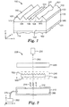
- FIG. 1 is a schematic side-view of a light redirecting film 100 for redirecting an incident light toward a desired direction.
- Light redirecting film 100 includes a first structured surface 110 that includes a plurality of microstructures 150 that extend along the y-direction.
- Light redirecting film 100 also includes a second structured surface 120 that is opposite the first structured surface 110 and includes a plurality of microstructures 160.
- Light redirecting film 100 also includes a substrate layer 170 that is disposed between respective first and second structured surfaces 110 and 120 and includes a first major surface 172 and an opposing second major surface 174.
- Light redirecting film 100 also includes a prism layer 130 that is disposed on first major surface 172 of the substrate layer and includes first structured surface 110 of the light redirecting film, and a structured layer 140 with a major surface 142 that is disposed on second major surface 174 of the substrate layer and includes structured surface 120 of the light redirecting film.
- the exemplary light redirecting film 100 includes three layers 130, 170 and 140.
- the light redirecting film can have one or more layers.
- the light redirecting film can have a single layer that includes respective first and second major surfaces 110 and 120.
- the light redirecting film can have many layers.
- substrate 170 can have multiple layers.
- structure 100 may be understood as a film stack.
- prismatic structured layer 130 may be understood as a first optical film.
- structured layer 140 may be understood as a second optical film disposed on and optically coupled to the first optical film.
- Microstructures 150 are primarily designed to redirect light that is incident on major surface 120 of the light redirecting film, along a desired direction, such as along the positive z-direction.
- microstructures 150 are prismatic linear structures.
- microstructures 150 can be any type microstructures that are capable of redirecting light by, for example, refracting a portion of an incident light and recycling a different portion of the incident light.
- the cross-sectional profiles of microstructures 150 can be or include curved and/or piece-wise linear portions.
- microstructures 150 can be linear cylindrical lenses extending along the y-direction.
- Each linear prismatic microstructure 150 includes an apex angle 152 and a height 154 measured from a common reference plane such as, for example, major plane surface 172.
- the height of a prismatic microstructure 150 can change along the y-direction.
- the prism height of prismatic linear microstructure 151 varies along the y-direction.
- prismatic microstructure 151 has a local height that varies along the y-direction, a maximum height 155, and an average height.
- a prismatic linear microstructure, such as linear microstructure 153 has a constant height along the y-direction. In such cases, the microstructure has a constant local height that is equal to the maximum height and the average height.
- some of the linear microstructures are shorter and some of the linear microstructures are taller.
- height 156 of linear microstructure 153 is smaller than height 158 of linear microstructure 157.
- the microstructures 160 on the surface of matte layer 140 may also be varied in height for reduction of optical coupling or wet-out.
- Apex or dihedral angle 152 can have any value that may be desirable in an application.
- apex angle 152 can be in a range from about 70 degrees to about 110 degrees, or from about 80 degrees to about 100 degrees, or from about 85 degrees to about 95 degrees.
- microstructures 150 have equal apex angles which can, for example, be in a range from about 88 or 89 degree to about 92 or 91 degrees, or can be about 90 degrees.
- Prism layer 130 can have any index of refraction that may be desirable in an application.
- the index of refraction of the prism layer is in a range from about 1.4 to about 1.8, or from about 1.5 to about 1.8, or from about 1.5 to about 1.7.
- the index of refraction of the prism layer is not less than about 1.5, or not less than about 1.55, or not less than about 1.6, or not less than about 1.65, or not less than about 1.7.
- the light redirecting film 100 can increase or improve the brightness of the display.
- the light redirecting film has an effective transmission (ET) or relative gain that is greater than 1.
- E effective transmission
- effective transmission is the ratio of the luminance of the display system with the film in place in the display system to the luminance of the display without the film in place.
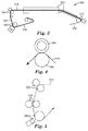
- Effective transmission can be measured using an optical system 200, a schematic side-view of which is shown in FIG. 2 .
- Optical system 200 is centered on an optical axis 250 and includes a hollow lambertian light box 210 that emits lambertian light 215 through an emitting or exit surface 212, a linear light absorbing polarizer 220, and a photo detector 230.
- Light box 210 is illuminated by a stabilized broadband light source 260 that is connected to an interior 280 of the light box via an optical fiber 270.
- a test sample of the ET which is to be measured by the optical system, is placed at location 240 between the light box and the absorbing linear polarizer.
- the ET of light redirecting film 100 can be measured by placing the light redirecting film at location 240 with linear prisms 150 facing the photo detector and microstructures 160 facing the light box. Next, the spectrally weighted axial luminance I 1 (luminance along optical axis 250) is measured through the linear absorbing polarizer by the photo detector. Next, the light redirecting film is removed and the spectrally weighted luminance I 2 is measured without the light redirecting film placed at location 240. ET is the ratio I 1 /I 2 .
- ET0 is the effective transmission when linear prisms 150 extend along a direction that is parallel to the polarizing axis of linear absorbing polarizer 220
- ET90 is the effective transmission when linear prisms 150 extend along a direction that is perpendicular to the polarizing axis of the linear absorbing polarizer.
- the average effective transmission (ETA) is the average of ET0 and ET90.
- Measured effective transmission values disclosed herein were measured using a SpectraScanTM PR-650 SpectraColorimeter (available from Photo Research, Inc, Chatsworth, CA) for photo detector 230.
- Light box 210 was a Teflon cube with a total reflectance of about 85%.
- the average effective transmission (ETA) of the light redirecting film is not less than about 1.5, or not less than about 1.55, or not less than about 1.6, or not less than about 1.65, or not less than about 1.7, or not less than about 1.75, or not less than about 1.8.
- the average effective transmission of the optical film or optical stack is less by no more than about 2% or less than about 1% or less than about 0.5% than an optical film or optical stack that has the comparable construction except for a smooth non-structured second surface rather than a microstructured second surface.
- "comparable construction" is actually the same construction in all respects except for the noted exception (e.g. here, a smooth non-structured second surface rather than a microstructured second surface).
- the average effective transmission of the optical film or optical stack is greater than an optical film or optical stack that has the same construction except for a smooth non-structured second surface rather than a microstructured second surface.
- the average effective transmission of the microstructured surface is at least 0.5% or at least 1.0% or at least 1.5% greater than a comparable stack with a smooth second surface.
- Optical haze is defined as the ratio of the transmitted light that deviates from the normal direction by more than 2.5 degrees to the total transmitted light. Haze values disclosed herein were measured using a Haze-Gard Plus haze meter (available from BYK-Gardiner, Silver Springs, Md.) according to the procedure described in ASTM D1003. Optical clarity, as used herein, refers to the ratio (T 1 -T 2 )/(T 1 +T 2 ), where T 1 is the transmitted light that deviates from the normal direction between 1.6 and 2 degrees from the normal direction, and T 2 is the transmitted light that lies between zero and 0.7 degrees from the normal direction. Clarity values disclosed herein were measured using a Haze-Gard Plus haze meter from BYK-Gardiner.
- Microstructures 160 on the optical structured surface primarily serve to hide undesirable physical defects (such as, for example, scratches) and/or optical defects (such as, for example, undesirably bright or "hot” spots from a lamp in a display or illumination system) with no, or very little, adverse effect on the capabilities of the light redirecting film to redirect light and enhance brightness.
- the structured surface comprising microstructures 160 has an optical haze of less than about 20%, or less than about 10%, or less than about 7.5%, or less than about 5% or less than about 3.5%, or less than about 3%, or less than about 2%, or less than about 1.5%, or less than about 1%.
- the surface has an optical haze of between about 0 and 1%, or an optical haze of between about 4% and 10%, or an optical haze of between about 10% and 18%.
- the structured surface comprising microstructures 160 has an optical clarity of less than about 90%, or less than about 80%, or less than about 75%, or less than about 70%, or less than about 65%, or less than about 60%, or less than about 55%, or less than about 50%, or less than about 45%, or less than about 40%. In some cases, the surface has an optical clarity of between about 75% and 95%, or between about 35% and 70%, or between about 30% and 55%, or between about 25% and 45%. In some cases, the optical clarity of the structured surface is less than the function: (- 3 x OpticalHaze)+ 80%. The optical clarity of the structure may also be less than the function (- 3 x OpticalHaze ) + 80% and greater than 20%.
- a high amount of the disclosed optical haze values and optical clarity values of the optical surface should be understood as being capable of being properties of a given film displayed with one another, that is, should be understood as being capable of independent control.
- a given structured surface may have an optical clarity of less than 90% and an optical haze of less than 10%, or an optical clarity of less than 90% and an optical haze of less than 5%.
- a given structured surface may have an optical haze of less than 5% and an optical clarity of less than 70%.
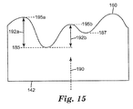
- microstructures 160 can have any height and any height distribution. Height itself may be defined as the distance (e.g. 192a, 192b) along a plane 190 orthogonal to the base of the material 142 from the lowest local minimum of the surface 185 in the area to an adjacent peak of the microstructure array (local maximum) 195a or 195b. Height is not measured from a local minimum that is not the lowest local minimum in the area, e.g. 187. Given the multiple heights 192 of peaks on the surface, an average height may be determined (where average height equals the total height of all peaks divided by number of peaks, e.g. (192a + 192b) / 2). In some cases, the average height of microstructures 160 is not greater than about 10 ⁇ m, or not greater than about 7.5 ⁇ m, or not greater than about 5 ⁇ m, or not greater than about 2.5 ⁇ m.
- the presently described matte films may also be understood as having microstructures that are randomly positioned across the surface of the film. Such randomization is important for mitigating the occurrence of Moiré interference patterns that result from periodic structures.
- One valuable way to measure the randomness of a surface is by creating a Fourier spectrum of the surface values.
- the process for measuring Fourier spectrum and deriving a randomness measurement may be understood by reference to Figs. 18-24 .
- Fig. 18 illustrates a topographic map of a film according to the present description.
- the topographic data i.e. height values
- Matlab a sophisticated calculation and manipulation program
- the Fourier spectrum can be calculated, and a 2-dimensional spectrum, such as that shown in Fig. 19 may be created.
- the spectrum of Fig. 27 is actually one taken from an Example illustrated below.
- the line profile through the 2-dimensional spectrum may then be determined in a series of directions, as illustrated in Fig. 20 . Only half of the spectrum must be investigated due to the symmetry of the spectrum.
- the total signal in each line profile is calculated, normalized by the length of the profile, and possibly by unequal frequency steps in the fx and fy directions, as shown in Fig. 21 .
- the maximum line profile 2110 is selected from this normalized sum.
- a Fourier spectrum line profile (in the direction of maximum signal) is plotted.
- the spectrum is median filtered to remove the effect of spikes on the steps below.
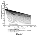
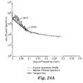
- the Fourier spectrum is shown in Fig. 22 .
- the median filtered spectrum is also illustrated. At this point, the user selects a point at or near the minimum just to the left of the peak in the spectrum and a local minimum is found. From this local minimum 2340, as illustrated in Fig.
- test lines segments are drawn for visualization from the local minimum 2340 to below the spectrum, and for each point on each line segment the distance between the spectrum and test line segment is calculated and the sum of distances for the closest 50% of points is calculated. These values are normalized by the lengths of the search lines.
- the minimum in the resulting curve corresponds to the test line that is closest to the spectrum. This line is considered tangent to the spectrum.
- the tangent line is applied to the graph in Figs. 24a and 24b .
- a search is performed along this tangent line for the portion that is closest to the spectrum. This position is the tangent position 2420.
- the local minimum to the left of the peak and the tangent position define the bounds of the peak, and the line between them defines a baseline.
- the ratio of the areas between the peak and the tangent line (shaded area 2410 in Fig. 24a ) and under the tangent line (shaded area 2430 in Fig. 24b ) is used to specify the strength of the periodicity of topography. These areas are calculated in linear (not log 10 ) units. For purposes of this disclosure, the ratio of the area between the peak and tangent line to the area under the tangent line may be referred to as RR 1 .
- RR 1 values are displayed versus the haze value of a given film.
- the RR 1 value is less than 2.
- the RR 1 value is less than 1.
- the RR 1 value may even be less than 0.5.
- Each of these values may be understood as corresponding to a strongly random arrangement (or non-periodic array). The lower the RR 1 value is, the less periodic the array of microstructures.
- This graph may be used to show the periodicity (or lack thereof) for at least some films of a given haze value disclosed herein.
- the film may have a RR 1 value is less than 2, or less than 1.
- substrate layer 170 may be useful to include substrate layer 170.
- the substrate may be valuable not only for structural purposes, but also in the process of developing and shaping the microstructured surface. Microstructured surface may be created in accordance with the methods described in commonly owned U.S. Patent Application No. 2009/0029054 , incorporated by reference herein in its entirety.
- substrate 170 may be any of a variety of materials suitable for use as a substrate, including flexible materials such as, for example, woven materials, knitted materials, films (e.g., polymeric films), nonwovens, metal sheet, metal foils, glass and the like.
- the substrate material will be chosen based in part on the desired optical and mechanical properties for the intended use.
- Suitable light transmissive optical films include without limitation multilayer optical and brightness enhancing films (e.g. reflective or absorbing), polarizing films, diffusive films and compensator films.
- Mechanical properties can include flexibility, dimensional stability and impact resistance.
- an optically clear material e.g., transparent may be desired.
- optically clear materials include optically clear polyester film, triacetate (TAC) film, polyethylene naphthalate, polyethylene terephthalate (PET), polycarbonate, cellulose acetate, poly(methyl methacrylate), polyolefins such as biaxially oriented polypropylene (BOPP) and simultaneously biaxially-oriented polypropylene (S-BOPP).
- the substrate 170 may comprise or consist of polyamides, polyimides, phenolic resins, polystyrene, styrene-acrylonitrile copolymers, epoxies, and the like.
- microstructured surface may be created in accordance with the methods described in commonly owned U.S. Patent Application No. 2009/0029054 .
- the structured surface may be formed by a process that begins with an initial coating on the substrate.
- the coating has its viscosity changed from a first viscosity to a second viscosity.
- the viscosity change may be understood as transitioning from a first viscosity, which is more liquid-like and capable of coating, to a second viscosity, which is more solid and therefore capable of retaining a structure, at least temporarily.
- the coating comes into contact with a face-side roller that imparts a microstructured finish on it.
- the coating may then optionally be hardened.
- the substrate used may be a substrate capable of hardening. This process may be better understood by reference to Fig. 3 .
- the microstructured surface will then have certain desirable material properties.
- Microstructured matte films produced according to this structure may be described as roll-induced matte optical structures.
- the apparatus for structuring the film is displayed as an apparatus 300 shown schematically in Fig. 3 .
- a coating is applied to a substrate 310 by a coating applicator 312.
- the viscosity of the coating which may generally be initially in a liquid state, is adjusted at a thickening station 314. This viscosity change (from a first viscosity to a second viscosity) may occur by removing volatile solvent from a resin solution, cooling a 100% solids resin, partial cross-linking a resin, warming a very high viscosity resin, combining two or more of these techniques, or other methods. After the viscosity change, the coated layer 316 is finished.
- a transformation station 318 that is generally a roller or nip.
- a close-up view of such a nip is illustrated in Fig. 4 .
- the nip has a face side roller 340 and a back-up roll 350 that the film 316 is rolled through.
- a first major surface of the coated substrate comes into contact with the face-side roller.
- Part of the coating layer is pulled away with the nip forming the remainder into a microstructured surface.
- the patterned coating 320 leaves the transformation station in a potentially less than solid state. Therefore, as illustrated in Fig. 3 , it is sent through a solidification station 330.
- Solidification may be performed by any number of suitable methods, including UV curing, thermal curing, electron beam curing, epoxy curing, further solvent removal, or others.
- the solidification station step results in a film with the pattern locked into
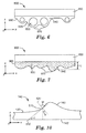
- a decoy nip may be added into the process that has been illustrated in Fig. 3 .
- Such a construction is illustrated in Fig. 5 .
- the film 510 is first passed through a decoy nip 520, before entering the transformation station nip 530.
- This construction may be desirable in situation where large dirt particles are arriving at the transformation station nip.
- the addition of the decoy nip may remove and collect dirt prior to structuring and transformation.
- the structure of the surface is again locked into place at a solidification station 540.
- the decoy nip is used to collect and remove defect causing debris and particles, such as dirt, from a liquid coating.
- the device is useful for improving the robustness of the structuring process in low cleanliness environments.
- the decoy nip has equal or higher affinity for particulates than the transformation station nip.
- the decoy nip removes debris from the liquid coating that would otherwise be captured on the transformation station nip without adversely affecting the final structured coating produced.
- the distance from the decoy roll nip to the transformation station roll nip can vary based upon the cleanliness of the manufacturing environment.
- Coatable materials suitable for use in the present description may comprise any of a variety of film forming materials.
- the coatable material is a polymeric material comprised of one or more polymers and/or oligomers in solvent.
- the coatable material is a mixture of one or more monomers, oligomers and/or polymers in one or more solvents.
- the coatable material includes the foregoing oligomer(s), monomer(s) and/or polymer(s) in one or more solvents along with a volume of particles or nanoparticles.
- the coatable materials may include photo initiators, cross-linkers, anti-static compounds, and other active materials.
- Nanoparticles can be surface modified which refers to the fact that the nanoparticles have a modified surface so that, for example, the nanoparticles provide a stable dispersion.
- “Stable dispersion” refers to a dispersion in which the colloidal nanoparticles do not agglomerate after standing for a period of time, such as about 24 hours, under ambient conditions, e.g., room temperature (about 20-22°C), and atmospheric pressure, without extreme electromagnetic forces.
- Surface-modified colloidal nanoparticles can optionally be present in a polymer coating used as a coatable composition herein with nanoparticles present in an amount effective to enhance the durability of the finished or optical element.
- the surface-modified colloidal nanoparticles described herein can have a variety of desirable attributes, including, for example, nanoparticle compatibility with a coatable composition such that the nanoparticles form stable dispersions within the coatable composition, reactivity of the nanoparticle with the coatable composition making the composite more durable, and a low impact or uncured composition viscosity.
- a combination of surface modifications can be used to manipulate the uncured and cured properties of the composition.
- Surface-modified nanoparticles can improve optical and physical properties of the coatable composition such as, for example, improved resin mechanical strength, minimized viscosity changes while increasing solids volume loading in the coatable composition and maintain optical clarity while increasing solid volume loading in the coatable composition.
- the nanoparticles are surface-modified nanoparticles.
- Suitable surface-modified colloidal nanoparticles can comprise oxide particles. Nanoparticles may comprise a range of particle sizes over a known particle size distribution for a given material. In some embodiments, the average particle size may be within a range from about 1 nm to about 100 nm. Particle sizes and particle size distributions may be determined in a known manner including, for example, by transmission electron microscopy (TEM).
- TEM transmission electron microscopy
- Suitable nanoparticles can comprise any of a variety of materials such as metal oxides selected from alumina, tin oxide, antimony oxide, silica, zirconia, titania and combinations of two or more of the foregoing. Surface-modified colloidal nanoparticles can be substantially fully condensed.
- silica nanoparticles can have a particle size ranging from about 5 to about 75 nm. In some embodiments, silica nanoparticles can have a particle size ranging from about 10 to about 30 nm. Silica nanoparticles can be present in the coatable composition in an amount from about 10 to about 100 phr. In some embodiments, silica nanoparticles can be present in the coatable composition in an amount from about 25 to about 80 phr, and in other embodiments, silica nanoparticles can be present in the coatable composition in an amount from about 30 to about 70 phr. Silica nanoparticles suitable for use in the coatable compositions of the present description are commercially available from Nalco Chemical Co.
- Suitable silica products include NALCO products 1040, 1042, 1050, 1060, 2327 and 2329.
- Suitable fumed silica products include for example, products sold under the trade name AEROSIL series OX-50, -130, -150, and -200 available from DeGussa AG, (Hanau, Germany), and CAB-O-SPERSE 2095, CAB-O-SPERSE A105, CAB-O-SIL MS available from Cabot Corp. (Tuscola, Ill.)
- Surface-treating the nanosized particles can provide a stable dispersion in the coatable composition (e.g., a polymeric resin).
- the surface-treatment stabilizes the nanoparticles so that the particles will be well dispersed in the coatable composition and results in a substantially homogeneous composition.
- the nanoparticles can be modified over at least a portion of its surface with a surface treatment agent so that the stabilized particle can copolymerize or react with the coatable composition during curing.
- a number of matte films include sufficiently large particles that the particles serve as the primary reason for formation of microstructures.
- Such a film is illustrated in Fig. 6 .
- the optical film 800 possesses substrate or first film 850 mechanically coupled to microstructured layer 860.
- particles 830 are dispersed in a binder 840. It may be noted that size of the particles 830 is very close in scale to the actually width or height of the microstructures 870.
- the current description provides for a structured surface 160 that has particles. However, the particles of the current description are small in relation to the thickness of the coating layer and thus do not serve as the primary reason for formation of the microstructures.
- Optical properties such as haze, clarity and transmission of matte coatings are controlled in part by the size of particles relative to the coating thickness, as well as the density and distribution of such particles.
- An example of a film designed according to the current description is illustrated in Fig. 7 .
- optical film or film stack 900 possesses substrate layer or first film 950 mechanically coupled to microstructured layer 960.
- Particles 930 are dispersed in a binder 940. It is readily apparent that the thickness of the layer at all points, and most especially at peaks of the microstructures 970 is much greater than the thickness of the particles 930. More specifically, the particles in the optical film have a size of less than 0.5 microns, or in some embodiments, less than 0.2 microns, or less than 0.1 microns.
- the structured surface will have an index of refraction of between about 1.50 and 1.70. In other embodiments the structured surface may have an index of refraction from as low as about 1.17 to as high as about 1.8.
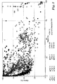
- Fig. 8 provides a full haze and clarity spectrum of a number of films developed according to the present description. It is illustrated in comparison to thirteen other structured films in order to illustrate the performance advantages over other structured films.
- Film 1 is a 3M bead coated matte film.
- Film 2 is a film with patterned white ink on PET.
- Film 3 is a Keiwa 100-BMUIS film.
- Film 4 is a bead-coated matte film.
- Film 5 is a particle bead coated matte film.
- Film 6 is a Kimoto 100TL4 film.
- Film 7 is a matte film created by flame embossing the surface of the film.
- Film 8 is a microreplicated matte film created using electro deposition.
- Film 9 is a film textured by application and removal of an extrudable, strippable skin.
- Film 10 is a microreplicated matte film.
- Film 11 is a matte film with dispersed beads in a gravure coating.
- Film 12 is a microreplicated, machined matte film.
- Film 13 is a Dai Nippon DNP M268Y film.
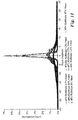
- Figs. 8 and 9 a great deal of films according to the current description display very low haze values, and high clarity values. In order to best understand this performance, Fig. 9 may be referenced. This figure provides a scaled haze percentage of 0 to 20%, and clarity range of 0 to 100%.
- Fig. 9 displays clearly the levels of performance that the current description reaches that other films do not.
- the film may be understood in one aspect as having an optical clarity value of less than 50% and an optical haze value of less than 10%.
- the film of the present description may be understood as having an optical haze of less than about 7.5% and an optical clarity of less than about 60%.
- Within this performance range there may fall one or two other films (e.g. 3M Particle Matte).
- any such film is distinguishable in that the current film displays this performance with a structured surface with particle sizes of less than about 0.5 microns, or less than about 0.2 microns.
- the film of the present description may be understood as having an optical haze of less than about 5% and an optical clarity of less than about 70%, where again the structured surface of the film is made up of particles of a size less than about 0.5 microns or less than about 0.2 microns.
- the film of the present description has an optical haze of less than about 3% and an optical clarity of less than about 65% or 75%.
- the film may be understood as possessing an optical haze of less than about 1.5% and an optical clarity of less than about 80%.
- the film may be understood as having an optical haze of less than about 1% and an optical clarity of less than about 90%.
- the current film may be understood as having an optical haze of less than about 20% and an optical clarity of less than about 40%.
- the film of the present description may be understood as having an optical clarity between about 75% and 95% and an optical haze of between about 0 and 1%, where the film is made up of particles of an average size less than about 0.5 microns.
- the film may have an optical clarity of between about 35% and 70% and an optical haze of between about 1% and 4%.
- the film may have an optical clarity of between about 30% and 55% and an optical haze of between about 4% and 10%, where the film is made up of particles of an average size less than about 0.5 microns.
- the film is again made up of particles with an average size of less than about 0.5 microns, where the film's optical clarity values are between about 25% and 45% and optical haze values are between about 10% and 18%.
- the second film has an optical clarity of less than about 85% and an optical haze of less than about 3.5%.
- FIG. 10 is a schematic side-view of a portion of matte layer 140.
- FIG. 10 shows a microstructure 160 in structured surface 120.
- Microstructure 160 has a slope distribution across the surface of the microstructure.
- Slope ⁇ is also the angle between tangent line 530 and major surface 142 of the matte layer.
- H(x,y) the height profile of the surface.
- Average x-slope and y-slope were evaluated in a 6 micron interval centered at each pixel.
- the micron interval may be chosen to be smaller, such as 2 microns, or 3 microns, so long as a constant interval is used.
- GradientMagnitude ⁇ H x y ⁇ x 2 + ⁇ H x y ⁇ y 2
- X-slope distributions and Y-slope distributions were calculated for a number of embodiments of the present description. These films had haze value of 0.7%, 1.2%, 1.6%, 8%, 23%, 40% and 80%.
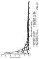
- Fig. 11 provides the x-slope distributions for these seven films produced in accordance with the present description.
- Fig. 12 provides the y-slope distributions for the same seven films. As is readily apparent from the two graphs, the majority of the film's surface has a slope that is very small in both the x and y directions. The films that possessed the lowest haze values (those 1.6% and below) also had the highest normalized count of area that fell at 0 degrees slope in both the x-slope distributions and y-slope distributions.
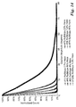
- Fig. 13 displays the gradient magnitude distributions. Again, the graph shows a high amount of surface for each of the films with very low slope. The greatest three peaks were for haze values of 1.6% haze, 1.2% haze and 0.7% haze. This data may be better understood by the corresponding Complement Cumulative Gradient Distribution (F CC ( ⁇ )). The F CC graph is shown in Fig. 14 . From this it was possible to determine various slopes of the surfaces according to given haze values of the films. Accordingly, the percentage of surface of the film that has a slope below a given number may be quantified according to the various haze values of the film.
- F CC Complement Cumulative Gradient Distribution
- films' surface slopes may be understood as correlated with haze values.
- the film may have at least 85% of the structured surface having a slope magnitude that is less than about 7.5 degrees.
- 95% of the structured surface has a slope magnitude that is less than about 10 degrees.
- 95% of the structured surface may have a slope magnitude that is less than about 5 degrees.
- haze value of the film are less than about 7.5%
- 90% of the structured surface may have a slope magnitude that is less than about 7.5 degrees.
- 97% of the structured surface may have a slope magnitude that is less than about 10 degrees.
- 95% of the structured surface may have a slope magnitude that is less than about 5 degrees.
- haze value of the film is less than about 5%
- 85% of the structured surface may have a slope magnitude that is less than about 5 degrees.
- 90% of the structured surface may have a slope that is less than about 5 degrees, or less than about 4 degrees.
- At least 90% of the structured surface may have a slope magnitude of less than about 5 degrees, or at least 95% of the structured surface may have a slope magnitude that is less than about 5 degrees.
- the haze value of the film is less than about 1.5%
- at least 80% of the structured surface may have a slope magnitude that is less than about 2.5 degrees.
- at least 98% of the structured surface may have a slope magnitude that is less than about 5 degrees.
- At least 90% of the structured surface may have a slope magnitude that is less than about 4 degrees, or 99% of the structured surface may have a slope magnitude less than about 5 degrees.
- At least 90% of the structured surface may have a slope magnitude that is less than about 7 degrees, or less than about 10 degrees.
- At least 50% of the optical film may be understood as having a slope of between about 1 degree and 5 degrees.
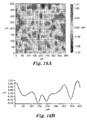
- Figs. 16a and 16c display atomic force microscopy images of a particular film according to the present description along the x and y-profiles.
- Figs. 16c and 16d provide the corresponding X and Y profiles of the film respectively.
- the particular film displayed in the figure had an optical haze of 0.7% and an optical clarity of 70.9%.
- the random distribution and random height changes of the film shown in the X and Y-profiles ( Figs. 16b and 16d ).
- the profile graphs may appear to have large slopes, the scales on the x and y-axes are vastly disproportionate.
- the steepest slope of the Y-profile moved from a height level of approximately +0.35 ⁇ m to -0.95 ⁇ m over a lateral range of approximately 300 ⁇ m to 350 ⁇ m. This equates to a negative slope of only -.026, and would further equate to a small angle from the plane of the film. Because y/x is equivalent to both slope and tangent of the slope angle, the arctan(.026) provides angle. Arctan(.026) more specifically provides for an angle 1.49 degrees.
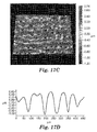
- Fig. 17a and 17c illustrate another image of a given film according to the current description.
- a Wyko phase-shift interferometer image was taken of the film along the x and y-profiles.
- the film had an optical haze value of 1.4% and an optical clarity value of 69.6%.
- the x and y-profiles displayed appeared to show more drastic slopes, again the axes were disproportionate in scale, such that a lateral move of 30 ⁇ m in the x-direction (270 to 300 ⁇ m) resulted in a z-change of 1.5 ⁇ m (-1.0 to +0.5) (see Fig. 17b ).
- the x-profile calculation above showed a slope of 0.05, which is equivalent to an angle (again calculated from arctangent) of 2.86 degrees.
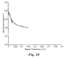
- FIG. 26 Another sample was measured of a film created in accordance with the present description.
- a scanning electron microscope image of the surface is shown in Fig. 26 .
- the sample was measured to have a haze value of 2.47% and an optical clarity value of 59.1 %.
- a Fourier spectrum was created for the film profile.
- a spectrum from this sample is shown in Fig. 27 . From this spectrum, again in accordance with the methods disclosed above and shown in Figs. 18-24a & b , the peak profile was created for the sample as illustrated in Fig. 28 . From this it was possible to determine that the Fourier ratio RR 1 value for the film profile was 0.65.
Landscapes
- Physics & Mathematics (AREA)
- General Physics & Mathematics (AREA)
- Optics & Photonics (AREA)
- Chemical & Material Sciences (AREA)
- Dispersion Chemistry (AREA)
- Engineering & Computer Science (AREA)
- Manufacturing & Machinery (AREA)
- Optical Elements Other Than Lenses (AREA)
- Laminated Bodies (AREA)
- Devices For Indicating Variable Information By Combining Individual Elements (AREA)
Applications Claiming Priority (2)
| Application Number | Priority Date | Filing Date | Title |
|---|---|---|---|
| US34923410P | 2010-05-28 | 2010-05-28 | |
| EP11721945.1A EP2577364B1 (en) | 2010-05-28 | 2011-05-17 | Light redirecting film and display system incorporating same |
Related Parent Applications (2)
| Application Number | Title | Priority Date | Filing Date |
|---|---|---|---|
| EP11721945.1A Division EP2577364B1 (en) | 2010-05-28 | 2011-05-17 | Light redirecting film and display system incorporating same |
| EP11721945.1A Division-Into EP2577364B1 (en) | 2010-05-28 | 2011-05-17 | Light redirecting film and display system incorporating same |
Publications (1)
| Publication Number | Publication Date |
|---|---|
| EP3125003A1 true EP3125003A1 (en) | 2017-02-01 |
Family
ID=44121292
Family Applications (2)
| Application Number | Title | Priority Date | Filing Date |
|---|---|---|---|
| EP11721945.1A Not-in-force EP2577364B1 (en) | 2010-05-28 | 2011-05-17 | Light redirecting film and display system incorporating same |
| EP16183364.5A Withdrawn EP3125003A1 (en) | 2010-05-28 | 2011-05-17 | Light redirecting film and display system incorporating same |
Family Applications Before (1)
| Application Number | Title | Priority Date | Filing Date |
|---|---|---|---|
| EP11721945.1A Not-in-force EP2577364B1 (en) | 2010-05-28 | 2011-05-17 | Light redirecting film and display system incorporating same |
Country Status (8)
| Country | Link |
|---|---|
| US (2) | US10156661B2 (enExample) |
| EP (2) | EP2577364B1 (enExample) |
| JP (1) | JP6018051B2 (enExample) |
| KR (1) | KR101851413B1 (enExample) |
| CN (1) | CN102906604B (enExample) |
| SG (1) | SG185719A1 (enExample) |
| TW (1) | TW201211589A (enExample) |
| WO (1) | WO2011149715A1 (enExample) |
Families Citing this family (10)
| Publication number | Priority date | Publication date | Assignee | Title |
|---|---|---|---|---|
| CN102460231B (zh) | 2009-06-02 | 2016-05-18 | 3M创新有限公司 | 光重新定向膜和使用此膜的显示器 |
| KR20120061911A (ko) | 2009-08-25 | 2012-06-13 | 쓰리엠 이노베이티브 프로퍼티즈 컴파니 | 광 방향 전환 필름 및 이를 포함하는 디스플레이 시스템 |
| US9383482B2 (en) | 2010-05-07 | 2016-07-05 | 3M Innovative Properties Company | Antireflective films comprising microstructured surface |
| WO2013096324A1 (en) * | 2011-12-21 | 2013-06-27 | 3M Innovative Properties Company | Optical film stack |
| BR112014016062B8 (pt) | 2011-12-29 | 2021-04-13 | 3M Innovative Properties Co | método para fabricação de um artigo limpável, artigo limpável e método para utilizar um artigo limpável |
| US9494817B2 (en) * | 2012-01-31 | 2016-11-15 | 3M Innovative Properties Company | Display with nonwoven diffuser |
| KR102109473B1 (ko) * | 2012-11-21 | 2020-05-12 | 쓰리엠 이노베이티브 프로퍼티즈 컴파니 | 광학 확산 필름 및 이를 제조하는 방법 |
| WO2014093119A1 (en) * | 2012-12-14 | 2014-06-19 | 3M Innovative Properties Company | Brightness enhancing film with embedded diffuser |
| DE102013003441A1 (de) * | 2013-02-25 | 2014-09-11 | Fraunhofer-Gesellschaft zur Förderung der angewandten Forschung e.V. | Elektromagnetische Strahlung streuendes Element |
| US12164120B2 (en) * | 2017-01-16 | 2024-12-10 | 3M Innovative Properties Company | Faceted microstructured surface |
Citations (7)
| Publication number | Priority date | Publication date | Assignee | Title |
|---|---|---|---|---|
| US6164785A (en) * | 1996-07-05 | 2000-12-26 | Dai Nippon Printing Co., Ltd. | Antiglaring film |
| JP2005092197A (ja) * | 2003-08-13 | 2005-04-07 | Sumitomo Chemical Co Ltd | 防眩性光学フィルム |
| US20070121211A1 (en) * | 2005-09-16 | 2007-05-31 | Fuji Photo Film Co., Ltd. | Antiglare antireflective film, polarizing plate and liquid crystal display |
| WO2008020610A1 (en) * | 2006-08-18 | 2008-02-21 | Dai Nippon Printing Co., Ltd. | Optical laminate, polarizer and image display unit |
| US20080212005A1 (en) * | 2007-03-01 | 2008-09-04 | Toppan Printing Co., Ltd. | Antiglare film |
| US20090029054A1 (en) | 2007-07-25 | 2009-01-29 | Yapel Robert A | System and method for making a film having a matte finish |
| WO2011028373A1 (en) * | 2009-08-25 | 2011-03-10 | 3M Innovative Properties Company | Light redirecting film and display system incorporating same |
Family Cites Families (27)
| Publication number | Priority date | Publication date | Assignee | Title |
|---|---|---|---|---|
| US5598280A (en) * | 1993-03-23 | 1997-01-28 | Dai Nippon Printing Co., Ltd. | Film lens and a surface light source using the same |
| JP3607759B2 (ja) * | 1995-09-08 | 2005-01-05 | 五洋紙工株式会社 | プリズムシート |
| US6280063B1 (en) * | 1997-05-09 | 2001-08-28 | 3M Innovative Properties Company | Brightness enhancement article |
| BR9906910A (pt) | 1998-01-13 | 2000-10-10 | Minnesota Mining & Mfg | Bloco de alimentação para fabricar uma pelìcula óptica de camada múltipla, e, processo para fabricar uma pelìcula óptica de camada múltipla |
| JP2003004903A (ja) * | 2001-06-21 | 2003-01-08 | Fuji Photo Film Co Ltd | 防眩フィルム、偏光板用保護フィルム、偏光板、および画像表示装置 |
| TWI461758B (zh) * | 2003-08-13 | 2014-11-21 | Sumitomo Chemical Co | 製備抗眩光學膜的方法 |
| TW200508707A (en) * | 2003-08-29 | 2005-03-01 | Ind Tech Res Inst | High brightness diffusing sheet |
| JP4384506B2 (ja) | 2004-01-06 | 2009-12-16 | ダイセル化学工業株式会社 | 防眩性膜 |
| JP4739719B2 (ja) | 2004-10-01 | 2011-08-03 | ダイセル化学工業株式会社 | 防眩性フィルム |
| KR20070112140A (ko) | 2005-02-22 | 2007-11-22 | 후지필름 가부시키가이샤 | 필름, 그 제조방법, 상기 필름을 사용한 편광판, 및 상기편광판을 사용한 액정 표시 장치 및 표시장치 |
| JP2007079533A (ja) | 2005-08-17 | 2007-03-29 | Fujifilm Corp | 光学樹脂フィルム、これを用いた偏光板および液晶表示装置 |
| CN100590458C (zh) * | 2005-08-17 | 2010-02-17 | 富士胶片株式会社 | 光学树脂膜以及使用该光学树脂膜的偏光膜和液晶显示装置 |
| JP2007108724A (ja) * | 2005-09-16 | 2007-04-26 | Fujifilm Corp | 防眩性反射防止フィルム、これを用いた偏光板および液晶表示装置 |
| JP2007187952A (ja) | 2006-01-16 | 2007-07-26 | Sumitomo Chemical Co Ltd | 防眩フィルム、その製造方法、そのための金型の製造方法、及び表示装置 |
| JP2007233185A (ja) | 2006-03-02 | 2007-09-13 | Fujifilm Corp | 光学フィルム、反射防止フィルム、偏光板および画像表示装置 |
| WO2007111026A1 (ja) * | 2006-03-29 | 2007-10-04 | Tomoegawa Co., Ltd. | 光学フィルム |
| TWI447442B (zh) | 2008-06-26 | 2014-08-01 | Eternal Chemical Co Ltd | 具有非球形粒子之光學薄膜 |
| CA2689032A1 (en) | 2007-06-04 | 2008-12-11 | Thomson Licensing | Film cleaning system |
| JP2009098657A (ja) * | 2007-09-26 | 2009-05-07 | Fujifilm Corp | 液晶表示装置 |
| JP5139781B2 (ja) | 2007-11-21 | 2013-02-06 | シャープ株式会社 | 機能性フィルム及び表示装置 |
| JP5188251B2 (ja) | 2008-04-22 | 2013-04-24 | 旭化成株式会社 | 防眩性フィルム |
| JP2010032739A (ja) * | 2008-07-29 | 2010-02-12 | Suntechopt Co Ltd | レンズフィルムおよびこれを備えた光学表示用バックライトユニット |
| JP2010066469A (ja) | 2008-09-10 | 2010-03-25 | Daicel Chem Ind Ltd | 防眩性フィルムおよびその製造方法 |
| KR101357380B1 (ko) | 2008-10-07 | 2014-02-03 | 다이니폰 인사츠 가부시키가이샤 | 광학 시트, 면 광원 장치 및 투과형 표시 장치 |
| JP5158443B2 (ja) | 2009-03-25 | 2013-03-06 | 住友化学株式会社 | 防眩フィルムおよびその製造方法、ならびに金型の製造方法 |
| CN102460231B (zh) * | 2009-06-02 | 2016-05-18 | 3M创新有限公司 | 光重新定向膜和使用此膜的显示器 |
| EP2493689A2 (en) * | 2009-10-27 | 2012-09-05 | 3M Innovative Properties Company | Optical film with anti-warp surface |
-
2011
- 2011-05-17 JP JP2013512658A patent/JP6018051B2/ja not_active Expired - Fee Related
- 2011-05-17 WO PCT/US2011/036825 patent/WO2011149715A1/en not_active Ceased
- 2011-05-17 EP EP11721945.1A patent/EP2577364B1/en not_active Not-in-force
- 2011-05-17 CN CN201180025462.3A patent/CN102906604B/zh active Active
- 2011-05-17 EP EP16183364.5A patent/EP3125003A1/en not_active Withdrawn
- 2011-05-17 US US13/700,572 patent/US10156661B2/en active Active
- 2011-05-17 KR KR1020127033371A patent/KR101851413B1/ko not_active Expired - Fee Related
- 2011-05-17 SG SG2012086195A patent/SG185719A1/en unknown
- 2011-05-27 TW TW100118727A patent/TW201211589A/zh unknown
-
2018
- 2018-11-09 US US16/186,046 patent/US11226433B2/en active Active
Patent Citations (7)
| Publication number | Priority date | Publication date | Assignee | Title |
|---|---|---|---|---|
| US6164785A (en) * | 1996-07-05 | 2000-12-26 | Dai Nippon Printing Co., Ltd. | Antiglaring film |
| JP2005092197A (ja) * | 2003-08-13 | 2005-04-07 | Sumitomo Chemical Co Ltd | 防眩性光学フィルム |
| US20070121211A1 (en) * | 2005-09-16 | 2007-05-31 | Fuji Photo Film Co., Ltd. | Antiglare antireflective film, polarizing plate and liquid crystal display |
| WO2008020610A1 (en) * | 2006-08-18 | 2008-02-21 | Dai Nippon Printing Co., Ltd. | Optical laminate, polarizer and image display unit |
| US20080212005A1 (en) * | 2007-03-01 | 2008-09-04 | Toppan Printing Co., Ltd. | Antiglare film |
| US20090029054A1 (en) | 2007-07-25 | 2009-01-29 | Yapel Robert A | System and method for making a film having a matte finish |
| WO2011028373A1 (en) * | 2009-08-25 | 2011-03-10 | 3M Innovative Properties Company | Light redirecting film and display system incorporating same |
Also Published As
| Publication number | Publication date |
|---|---|
| SG185719A1 (en) | 2012-12-28 |
| JP2013535021A (ja) | 2013-09-09 |
| US11226433B2 (en) | 2022-01-18 |
| US20190094418A1 (en) | 2019-03-28 |
| EP2577364A1 (en) | 2013-04-10 |
| KR101851413B1 (ko) | 2018-04-23 |
| US10156661B2 (en) | 2018-12-18 |
| KR20130092428A (ko) | 2013-08-20 |
| US20130070341A1 (en) | 2013-03-21 |
| CN102906604A (zh) | 2013-01-30 |
| CN102906604B (zh) | 2016-04-27 |
| WO2011149715A1 (en) | 2011-12-01 |
| JP6018051B2 (ja) | 2016-11-02 |
| TW201211589A (en) | 2012-03-16 |
| EP2577364B1 (en) | 2016-09-28 |
Similar Documents
| Publication | Publication Date | Title |
|---|---|---|
| US11226433B2 (en) | Light redirecting film and display system incorporating same | |
| US20130201660A1 (en) | Optical film with anti-warp surface | |
| TWI628457B (zh) | 防眩膜、偏光板、液晶面板以及影像顯示裝置 | |
| JP6212844B2 (ja) | 光学フィルム、偏光板、液晶パネルおよび画像表示装置 | |
| TWI507728B (zh) | 光轉向膜及包含其之顯示系統 | |
| US9389355B2 (en) | Structured optical film | |
| KR102262757B1 (ko) | 터치 패널, 표시 장치 및 광학 시트, 광학 시트의 선별 방법 및 광학 시트의 제조 방법 | |
| US10928563B2 (en) | Microstructured diffuser comprising first microstructured layer and coating, optical stacks, and method | |
| KR102593914B1 (ko) | 방현 필름 및 그것을 사용한 표시 장치 | |
| KR20130105510A (ko) | 광학 필름, 편광판, 액정 패널 및 화상 표시 장치 | |
| WO2011028373A1 (en) | Light redirecting film and display system incorporating same | |
| KR102382755B1 (ko) | 터치 패널, 표시 장치 및 광학 시트, 그리고 광학 시트의 선별 방법 및 광학 시트의 제조 방법 | |
| WO2020246314A1 (ja) | 防眩フィルム、並びにそれを用いた防眩性物品、タッチパネル及び表示装置、並びに防眩フィルムの選定方法 | |
| CN118625427B (zh) | 光学膜、图像显示面板以及图像显示装置 | |
| CN118302699A (zh) | 光学膜、图像显示面板以及图像显示装置 |
Legal Events
| Date | Code | Title | Description |
|---|---|---|---|
| PUAI | Public reference made under article 153(3) epc to a published international application that has entered the european phase |
Free format text: ORIGINAL CODE: 0009012 |
|
| STAA | Information on the status of an ep patent application or granted ep patent |
Free format text: STATUS: THE APPLICATION HAS BEEN PUBLISHED |
|
| AC | Divisional application: reference to earlier application |
Ref document number: 2577364 Country of ref document: EP Kind code of ref document: P |
|
| AK | Designated contracting states |
Kind code of ref document: A1 Designated state(s): AL AT BE BG CH CY CZ DE DK EE ES FI FR GB GR HR HU IE IS IT LI LT LU LV MC MK MT NL NO PL PT RO RS SE SI SK SM TR |
|
| STAA | Information on the status of an ep patent application or granted ep patent |
Free format text: STATUS: REQUEST FOR EXAMINATION WAS MADE |
|
| 17P | Request for examination filed |
Effective date: 20170724 |
|
| RBV | Designated contracting states (corrected) |
Designated state(s): AL AT BE BG CH CY CZ DE DK EE ES FI FR GB GR HR HU IE IS IT LI LT LU LV MC MK MT NL NO PL PT RO RS SE SI SK SM TR |
|
| STAA | Information on the status of an ep patent application or granted ep patent |
Free format text: STATUS: EXAMINATION IS IN PROGRESS |
|
| 17Q | First examination report despatched |
Effective date: 20190403 |
|
| STAA | Information on the status of an ep patent application or granted ep patent |
Free format text: STATUS: THE APPLICATION HAS BEEN WITHDRAWN |
|
| 18W | Application withdrawn |
Effective date: 20190812 |