EP3117454B1 - Patterned wafer geometry measurements for semiconductor process controls - Google Patents
Patterned wafer geometry measurements for semiconductor process controls Download PDFInfo
- Publication number
- EP3117454B1 EP3117454B1 EP15811731.7A EP15811731A EP3117454B1 EP 3117454 B1 EP3117454 B1 EP 3117454B1 EP 15811731 A EP15811731 A EP 15811731A EP 3117454 B1 EP3117454 B1 EP 3117454B1
- Authority
- EP
- European Patent Office
- Prior art keywords
- wafer
- flatness
- site
- lithography
- error
- Prior art date
- Legal status (The legal status is an assumption and is not a legal conclusion. Google has not performed a legal analysis and makes no representation as to the accuracy of the status listed.)
- Active
Links
Images


Classifications
-
- H—ELECTRICITY
- H10—SEMICONDUCTOR DEVICES; ELECTRIC SOLID-STATE DEVICES NOT OTHERWISE PROVIDED FOR
- H10P—GENERIC PROCESSES OR APPARATUS FOR THE MANUFACTURE OR TREATMENT OF DEVICES COVERED BY CLASS H10
- H10P74/00—Testing or measuring during manufacture or treatment of wafers, substrates or devices
- H10P74/20—Testing or measuring during manufacture or treatment of wafers, substrates or devices characterised by the properties tested or measured, e.g. structural or electrical properties
- H10P74/203—Structural properties, e.g. testing or measuring thicknesses, line widths, warpage, bond strengths or physical defects
-
- H—ELECTRICITY
- H10—SEMICONDUCTOR DEVICES; ELECTRIC SOLID-STATE DEVICES NOT OTHERWISE PROVIDED FOR
- H10P—GENERIC PROCESSES OR APPARATUS FOR THE MANUFACTURE OR TREATMENT OF DEVICES COVERED BY CLASS H10
- H10P52/00—Grinding, lapping or polishing of wafers, substrates or parts of devices
-
- H—ELECTRICITY
- H10—SEMICONDUCTOR DEVICES; ELECTRIC SOLID-STATE DEVICES NOT OTHERWISE PROVIDED FOR
- H10P—GENERIC PROCESSES OR APPARATUS FOR THE MANUFACTURE OR TREATMENT OF DEVICES COVERED BY CLASS H10
- H10P52/00—Grinding, lapping or polishing of wafers, substrates or parts of devices
- H10P52/40—Chemomechanical polishing [CMP]
- H10P52/402—Chemomechanical polishing [CMP] of semiconductor materials
-
- H—ELECTRICITY
- H10—SEMICONDUCTOR DEVICES; ELECTRIC SOLID-STATE DEVICES NOT OTHERWISE PROVIDED FOR
- H10P—GENERIC PROCESSES OR APPARATUS FOR THE MANUFACTURE OR TREATMENT OF DEVICES COVERED BY CLASS H10
- H10P72/00—Handling or holding of wafers, substrates or devices during manufacture or treatment thereof
- H10P72/06—Apparatus for monitoring, sorting, marking, testing or measuring
-
- H—ELECTRICITY
- H10—SEMICONDUCTOR DEVICES; ELECTRIC SOLID-STATE DEVICES NOT OTHERWISE PROVIDED FOR
- H10P—GENERIC PROCESSES OR APPARATUS FOR THE MANUFACTURE OR TREATMENT OF DEVICES COVERED BY CLASS H10
- H10P74/00—Testing or measuring during manufacture or treatment of wafers, substrates or devices
- H10P74/23—Testing or measuring during manufacture or treatment of wafers, substrates or devices characterised by multiple measurements, corrections, marking or sorting processes
-
- H—ELECTRICITY
- H10—SEMICONDUCTOR DEVICES; ELECTRIC SOLID-STATE DEVICES NOT OTHERWISE PROVIDED FOR
- H10P—GENERIC PROCESSES OR APPARATUS FOR THE MANUFACTURE OR TREATMENT OF DEVICES COVERED BY CLASS H10
- H10P74/00—Testing or measuring during manufacture or treatment of wafers, substrates or devices
- H10P74/27—Structural arrangements therefor
- H10P74/277—Circuits for electrically characterising or monitoring manufacturing processes, e.g. circuits in tested chips or circuits in testing wafers
Definitions
- the disclosure generally relates to the field of semiconductors, and particularly to wafer geometry measurement techniques.
- Fabricating semiconductor devices typically includes processing a substrate such as a semiconductor wafer using a number of semiconductor fabrication processes.
- lithography is a semiconductor fabrication process that involves transferring a pattern from a reticle to a resist arranged on a semiconductor wafer.
- Additional examples of semiconductor fabrication processes include, but are not limited to, chemical-mechanical polishing (CMP), etching, deposition, and ion implantation.
- CMP chemical-mechanical polishing
- etching etching
- deposition deposition
- ion implantation ion implantation
- Metrology processes are used at various steps during a semiconductor manufacturing process to monitor and control one or more semiconductor layer processes. Some of these characteristics include the flatness and thickness uniformity of the wafers. While conventional metrology systems may be able to monitor and control these characteristics, they are generally utilized for handling unpatterned/bare wafers. Therein lies a need for systems and methods for wafer geometry measurements suitable for any wafers, including patterned wafers, without the aforementioned shortcomings.
- US2004/185662 discloses a wafer flatness evaluation method includes measuring front and rear surface shapes of a wafer. The wafer front surface measured is divided into sites. Then, a flatness calculating method is selected according to a position of the site to be evaluated and flatness in the wafer surface is acquired.
- US 2005/255610 A1 discloses a wafer flatness evaluation method comprising measuring frontside and backside heights.
- Embodiments of the present disclosure are directed to systems and methods for providing improved wafer geometry measurements for lithography focus, CMP, and other semiconductor process control scanner corrections.
- wafer geometry in the present disclosure refers to wafer front side height, backside height, thickness variation, flatness, and all consequent derivatives such as shape, topography, or the like.
- systems and methods in accordance with embodiments of the present disclosure are suitable for handling any types of wafers, including patterned wafers, without the shortcomings of conventional metrology systems.
- a patterned wafer geometry measurement tool utilized in accordance with the present disclosure is a measurement tool that is able to measure front side height, back side height, and thickness variation of the wafer. Obtaining such information allows the sources of flatness errors to be separated and attributed to front side and backside components.
- FIG. 2 a simplified illustration depicting a wafer 200 being polished by a polishing tool (e.g., CMP) is shown.
- a polishing tool e.g., CMP
- the polishing tool will then remove the raised portions of the top surface, resulting in a polished wafer 202 with a flat front side.
- this polished wafer 202 is undesirable because its flatness profile is suboptimal.
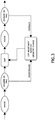
- FIG. 3 is an illustration depicting such a control loop. More specifically, the separate front side and backside topography measurement data can be obtained and feed to the control loop to optimize the polishing process. For instance, the control loop may calculate a best-flatness condition that can be achieved if the wafer is polished in a certain manner. Subsequently, different pressure levels can be applied to different areas of the wafer so that the best-flatness condition can be achieved as an end result, as opposed to simply providing a flat top surface 202 as depicted in FIG. 2 . In addition, wafer geometry measurements can be taken again after the polishing process; and adjustments necessary can be determined and applied to the polishing process accordingly.
- a polished wafer will be held on a vacuum or a chuck using force when it is processed by a lithography process tool or the like. It is noted that when the wafer is held on a chuck using force, the wafer backside is expected to be substantially flattened, and if the wafer was simply polished to provide a flat top surface, the top surface may no longer be flat when the wafer is chucked. Focus errors may be introduced as a result. Since wafer flatness errors directly contribute to focus errors during lithography exposure, configuring the polishing tool based on optimizing flatness conditions as described above effectively improves focus of the lithography process tool.
- the sources of flatness errors can be isolated.
- a subsequent process step may be notified of this observation (e.g., in a feedforward manner) and the subsequent process step may choose to compensate for (or avoid) such flatness errors accordingly.
- separating the front side topography from the backside topography can also help identifying process steps that may have caused front side and/or backside flatness errors during the manufacturing process.
- an analysis process may be invoked to find the cause of such signatures.
- this analysis process may be referred to as a cause analysis or root cause analysis
- this analysis process may take wafer geometry measurements at suspected process steps and identify the process step(s) that caused the backside signatures. It is contemplated that this process may also be utilized to analyze the front side errors as well.
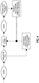
- FIGS. 3 and 4 are illustrations depicting control loops that may be utilized to analyze/assess wafer geometry variations induced by various types of process steps.
- the variations induced by that particular process step to wafer geometry can be assessed.
- the measured changes in wafer geometry may be related to impact on critical semiconductor fabrication parameters such as lithography focus and overlay errors, and yield by way of metrics such as site-flatness, in-plane displacement and the like that may be computed from the measured wafer geometry changes.
- this analysis process may be utilized in every critical process steps during the manufacturing process to catch potential errors as soon as possible.
- this analysis process may be conditionally invoked when certain signatures are detected on either the front side or the backside.
- this detection may prompt further analysis to find the cause of such signatures.
- it may be configured to manually and/or automatically adjust process step conditions for a particular process tool and thereby minimize the impact of that particular process tool on wafer geometry and certain critical semiconductor fabrication parameters.
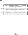
- FIG. 5 shows a methodology in which wafer flatness measurements obtained using a wafer geometry tool and scanner leveling measurements obtained from the lithography scanner can be used to calculate/estimate flatness errors. It is contemplated that patterned wafers or unpatterned bare wafers (serving as reference wafers) may be used to extract the flatness signature induced by a given chuck in step 502. Once the flatness signature of the given chuck has been extracted, total flatness errors during lithography exposures for future wafers chucked on that same chuck may be estimated.
- the wafer geometry can be obtained in step 504 using a wafer geometry tool.
- the total flatness error (representing the flatness errors when the wafer is chucked) can be calculated in step 506.
- the effects of forcing the wafer onto the chuck can be quantified (e.g., as a part of the feedforward control), which can help providing better focus leveling corrections.
- this calculation is also fully reversible. That is, if the height of the top surface is measured when the wafer is chucked on a particular chuck (e.g., based on scanner leveling measurements), and if the wafer geometry has been measured when the wafer was in an unchucked state, the flatness signature of that particular chuck can be calculated by subtracting the measured wafer geometry from the leveling map obtained from the lithography scanner. As previously mentioned, this process can be carried out using reference wafers in a controlled manner, and the extracted flatness signature of that particular chuck can be used to predict/estimate its effects on future wafers. In addition, the accuracy of this estimation process can be improved utilizing a feedback loop (e.g., as shown in FIG. 4 ).
- focus error and/or critical dimension uniformity can be measured post-lithography to check how well the feedforward focus corrections worked. If it is determined that the feedforward alone did not sufficiently reduce focus and/or critical dimension uniformity errors, then the feedback loop may be employed that will adjust the focus corrections for the next wafer.
- a site-based flatness variation metric is obtained, which can be used to perform root cause analysis and/or provided as feedback to improve the manufacturing processes.
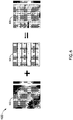
- a wafer-level thickness variation map is obtained and divided into a plurality of uniform sized sites (may also be referred to as fields). The thickness variation within each particular site is then leveled by fitting a single least-square best-fit plane to that particular site.
- each site is further divided into rectangular areas generally equivalent to the slit-size of the lithography scanner. It is understood that if a site cannot be evenly divided by the slit-size, a partial slit may be utilized on one end of the site, or the slit-size may be slightly adjusted to evenly divide the site. It is noted that one of the advantages provided by dividing the sites in this manner is that it simulates the scanning process, which is done in a slit-by-slit manner.
- each slit-area can be further leveled independently by fitting a single least-square best-fit plane to that particular slit-area in step 606, and the independently leveled slit-areas within each site can be combined to form a full wafer map (e.g., representing industry standard metrics such as site frontside least squares focal plane, or SFQ and the like) in step 608.
- a full wafer map e.g., representing industry standard metrics such as site frontside least squares focal plane, or SFQ and the like
- an average site-flatness value is taken by averaging all site-flatness values in step 610. It is noted that this average site-flatness value is leveled utilizing both conventional site-wise leveling and slit-by-slit leveling (which has the advantage of simulating the scanning process) as described above.
- the average site-flatness value calculated in this manner can be utilized to compute various derived metrics and information regarding a given wafer. For instance, by subtracting the average value from each site-based value, as shown in step 612, a site-to-site variation map can be calculated for the full wafer. It is also contemplated that while flatness values are used as exemplary measurement metrics, this site-based, slit-by-slit variation calculation process is applicable for calculation of various other types of measurement metrics, including, but not limited to flatness variations, thickness variations, as well as various other types of wafer topography variations that correlate to non-correctable focus errors seen by the lithography scanner during wafer exposure.
- these variation maps can be used for reporting purposes, and can also be analyzed to improve the manufacturing processes.
- the topography variation which is systematic
- any process variability (such as a local hot-spot created by a polishing tool) becomes visible after the systematic topography is removed. This information can then be provided as a feedback control to the polishing tool, thereby improving future processes.
- the average-site and site-to-site variation maps and metrics are not limited to flatness measurements.
- the same techniques described above are also applicable to other metrics for front side and/or backside maps such front and/or back nanotopography and the like.
- wafer used in the present disclosure may include a thin slice of semiconductor material used in the fabrication of integrated circuits and other devices, as well as other thin polished plates such as magnetic disc substrates, gauge blocks and the like.
- the methods disclosed may be implemented in various wafer geometry measurement tools as sets of instructions executed by one or more processors, through a single production device, and/or through multiple production devices. Further, it is understood that the specific order or hierarchy of steps in the methods disclosed are examples of exemplary approaches. Based upon design preferences, it is understood that the specific order or hierarchy of steps in the method can be rearranged. The accompanying method claims present elements of the various steps in a sample order, and are not necessarily meant to be limited to the specific order or hierarchy presented.
Landscapes
- Testing Or Measuring Of Semiconductors Or The Like (AREA)
- Length Measuring Devices With Unspecified Measuring Means (AREA)
- Exposure And Positioning Against Photoresist Photosensitive Materials (AREA)
- Mechanical Treatment Of Semiconductor (AREA)
- Engineering & Computer Science (AREA)
- Automation & Control Theory (AREA)
- Manufacturing & Machinery (AREA)
- Finish Polishing, Edge Sharpening, And Grinding By Specific Grinding Devices (AREA)
Priority Applications (1)
| Application Number | Priority Date | Filing Date | Title |
|---|---|---|---|
| EP20177916.2A EP3748669A1 (en) | 2014-06-24 | 2015-04-23 | Predictive modeling based focus error prediction |
Applications Claiming Priority (2)
| Application Number | Priority Date | Filing Date | Title |
|---|---|---|---|
| US14/313,733 US10576603B2 (en) | 2014-04-22 | 2014-06-24 | Patterned wafer geometry measurements for semiconductor process controls |
| PCT/US2015/027182 WO2015199801A1 (en) | 2014-06-24 | 2015-04-23 | Patterned wafer geometry measurements for semiconductor process controls |
Related Child Applications (1)
| Application Number | Title | Priority Date | Filing Date |
|---|---|---|---|
| EP20177916.2A Division EP3748669A1 (en) | 2014-06-24 | 2015-04-23 | Predictive modeling based focus error prediction |
Publications (3)
| Publication Number | Publication Date |
|---|---|
| EP3117454A1 EP3117454A1 (en) | 2017-01-18 |
| EP3117454A4 EP3117454A4 (en) | 2017-10-18 |
| EP3117454B1 true EP3117454B1 (en) | 2020-06-03 |
Family
ID=54979333
Family Applications (2)
| Application Number | Title | Priority Date | Filing Date |
|---|---|---|---|
| EP15811731.7A Active EP3117454B1 (en) | 2014-06-24 | 2015-04-23 | Patterned wafer geometry measurements for semiconductor process controls |
| EP20177916.2A Pending EP3748669A1 (en) | 2014-06-24 | 2015-04-23 | Predictive modeling based focus error prediction |
Family Applications After (1)
| Application Number | Title | Priority Date | Filing Date |
|---|---|---|---|
| EP20177916.2A Pending EP3748669A1 (en) | 2014-06-24 | 2015-04-23 | Predictive modeling based focus error prediction |
Country Status (4)
| Country | Link |
|---|---|
| EP (2) | EP3117454B1 (https=) |
| JP (1) | JP6650889B2 (https=) |
| KR (1) | KR102184033B1 (https=) |
| WO (1) | WO2015199801A1 (https=) |
Cited By (1)
| Publication number | Priority date | Publication date | Assignee | Title |
|---|---|---|---|---|
| WO2023022898A1 (en) * | 2021-08-16 | 2023-02-23 | Memc Llc | Systems and methods for processing semiconductor wafers using front-end processed wafer geometry metrics |
Families Citing this family (3)
| Publication number | Priority date | Publication date | Assignee | Title |
|---|---|---|---|---|
| US11556738B2 (en) * | 2020-10-01 | 2023-01-17 | Kla Corporation | System and method for determining target feature focus in image-based overlay metrology |
| CN118092089B (zh) * | 2024-04-23 | 2024-06-28 | 南京禄宪自动化科技有限公司 | 一种光刻晶片性能测试分析系统 |
| CN121348674B (zh) * | 2025-12-19 | 2026-04-10 | 合肥晶合集成电路股份有限公司 | 曝光机焦平面的补偿方法及装置、曝光方法 |
Family Cites Families (17)
| Publication number | Priority date | Publication date | Assignee | Title |
|---|---|---|---|---|
| JP3316833B2 (ja) * | 1993-03-26 | 2002-08-19 | 株式会社ニコン | 走査露光方法、面位置設定装置、走査型露光装置、及び前記方法を使用するデバイス製造方法 |
| JP2000094301A (ja) * | 1998-09-22 | 2000-04-04 | Canon Inc | 基板研磨方法および基板研磨装置 |
| JP2002018701A (ja) * | 2000-07-12 | 2002-01-22 | Canon Inc | 基板研磨方法および基板研磨装置 |
| US6859260B2 (en) * | 2001-04-25 | 2005-02-22 | Asml Holding N.V. | Method and system for improving focus accuracy in a lithography system |
| DE10314212B4 (de) * | 2002-03-29 | 2010-06-02 | Hoya Corp. | Verfahren zur Herstellung eines Maskenrohlings, Verfahren zur Herstellung einer Transfermaske |
| JP2004029735A (ja) * | 2002-03-29 | 2004-01-29 | Hoya Corp | 電子デバイス用基板、該基板を用いたマスクブランクおよび転写用マスク、並びにこれらの製造方法、研磨装置および研磨方法 |
| JP4464033B2 (ja) * | 2002-06-13 | 2010-05-19 | 信越半導体株式会社 | 半導体ウエーハの形状評価方法及び形状評価装置 |
| JP3769262B2 (ja) * | 2002-12-20 | 2006-04-19 | 株式会社東芝 | ウェーハ平坦度評価方法、その評価方法を実行するウェーハ平坦度評価装置、その評価方法を用いたウェーハの製造方法、その評価方法を用いたウェーハ品質保証方法、その評価方法を用いた半導体デバイスの製造方法、およびその評価方法によって評価されたウェーハを用いた半導体デバイスの製造方法 |
| JP4652667B2 (ja) * | 2003-02-13 | 2011-03-16 | キヤノン株式会社 | 面位置計測方法及び走査型露光装置 |
| SG123601A1 (en) * | 2003-03-10 | 2006-07-26 | Asml Netherlands Bv | Focus spot monitoring in a lithographic projectionapparatus |
| JP4615225B2 (ja) * | 2004-01-09 | 2011-01-19 | 株式会社ディスコ | 板状物に形成された電極の加工装置,板状物に形成された電極の加工方法,及び板状物に形成された電極の加工装置のチャックテーブルの平面度測定方法 |
| US20050255160A1 (en) | 2004-05-11 | 2005-11-17 | Stephen Bell | Polymide resin dermal composition |
| JP2006300676A (ja) * | 2005-04-19 | 2006-11-02 | Nikon Corp | 平坦度異常検出方法及び露光装置 |
| US8111376B2 (en) * | 2007-05-30 | 2012-02-07 | Kla-Tencor Corporation | Feedforward/feedback litho process control of stress and overlay |
| US8768665B2 (en) * | 2010-01-08 | 2014-07-01 | Kla-Tencor Technologies Corporation | Site based quantification of substrate topography and its relation to lithography defocus and overlay |
| JP2011249627A (ja) * | 2010-05-28 | 2011-12-08 | Toshiba Corp | 半導体ウェーハのパターン露光方法 |
| US9087176B1 (en) * | 2014-03-06 | 2015-07-21 | Kla-Tencor Corporation | Statistical overlay error prediction for feed forward and feedback correction of overlay errors, root cause analysis and process control |
-
2015
- 2015-04-23 KR KR1020167033676A patent/KR102184033B1/ko active Active
- 2015-04-23 EP EP15811731.7A patent/EP3117454B1/en active Active
- 2015-04-23 JP JP2016575021A patent/JP6650889B2/ja active Active
- 2015-04-23 EP EP20177916.2A patent/EP3748669A1/en active Pending
- 2015-04-23 WO PCT/US2015/027182 patent/WO2015199801A1/en not_active Ceased
Non-Patent Citations (1)
| Title |
|---|
| None * |
Cited By (3)
| Publication number | Priority date | Publication date | Assignee | Title |
|---|---|---|---|---|
| WO2023022898A1 (en) * | 2021-08-16 | 2023-02-23 | Memc Llc | Systems and methods for processing semiconductor wafers using front-end processed wafer geometry metrics |
| US12385850B2 (en) | 2021-08-16 | 2025-08-12 | Globalwafers Co., Ltd. | Semiconductor wafers using front-end processed wafer global geometry metrics |
| US12487185B2 (en) | 2021-08-16 | 2025-12-02 | Globalwafers Co., Ltd. | Systems and methods for processing semiconductor wafers using front-end processed wafer edge geometry metrics |
Also Published As
| Publication number | Publication date |
|---|---|
| KR20170018313A (ko) | 2017-02-17 |
| EP3748669A1 (en) | 2020-12-09 |
| EP3117454A4 (en) | 2017-10-18 |
| WO2015199801A1 (en) | 2015-12-30 |
| JP2017529681A (ja) | 2017-10-05 |
| EP3117454A1 (en) | 2017-01-18 |
| KR102184033B1 (ko) | 2020-11-27 |
| JP6650889B2 (ja) | 2020-02-19 |
Similar Documents
| Publication | Publication Date | Title |
|---|---|---|
| US10576603B2 (en) | Patterned wafer geometry measurements for semiconductor process controls | |
| US9779202B2 (en) | Process-induced asymmetry detection, quantification, and control using patterned wafer geometry measurements | |
| JP7227992B2 (ja) | 表面形状由来のオーバーレイの分解分析および分解分析を用いたオーバーレイ制御の向上 | |
| TWI604545B (zh) | 使用晶圓尺寸幾何工具之晶圓高階形狀特徵化及晶圓分類之系統,方法及度量 | |
| KR20140069352A (ko) | 신규 웨이퍼 지오메트리 메트릭을 이용한 오버레이 및 반도체 처리 제어 | |
| EP3117454B1 (en) | Patterned wafer geometry measurements for semiconductor process controls | |
| WO2016089786A1 (en) | Predicting and controlling critical dimension issues and pattern defectivity in wafers using interferometry | |
| CN108885407B (zh) | 叠加方差稳定化方法及系统 |
Legal Events
| Date | Code | Title | Description |
|---|---|---|---|
| STAA | Information on the status of an ep patent application or granted ep patent |
Free format text: STATUS: THE INTERNATIONAL PUBLICATION HAS BEEN MADE |
|
| PUAI | Public reference made under article 153(3) epc to a published international application that has entered the european phase |
Free format text: ORIGINAL CODE: 0009012 |
|
| STAA | Information on the status of an ep patent application or granted ep patent |
Free format text: STATUS: REQUEST FOR EXAMINATION WAS MADE |
|
| 17P | Request for examination filed |
Effective date: 20161014 |
|
| AK | Designated contracting states |
Kind code of ref document: A1 Designated state(s): AL AT BE BG CH CY CZ DE DK EE ES FI FR GB GR HR HU IE IS IT LI LT LU LV MC MK MT NL NO PL PT RO RS SE SI SK SM TR |
|
| AX | Request for extension of the european patent |
Extension state: BA ME |
|
| DAV | Request for validation of the european patent (deleted) | ||
| DAX | Request for extension of the european patent (deleted) | ||
| A4 | Supplementary search report drawn up and despatched |
Effective date: 20170920 |
|
| RIC1 | Information provided on ipc code assigned before grant |
Ipc: H01L 21/66 20060101AFI20170914BHEP |
|
| RIN1 | Information on inventor provided before grant (corrected) |
Inventor name: SINHA, JAYDEEP Inventor name: VUKKADALA, PRADEEP |
|
| GRAP | Despatch of communication of intention to grant a patent |
Free format text: ORIGINAL CODE: EPIDOSNIGR1 |
|
| STAA | Information on the status of an ep patent application or granted ep patent |
Free format text: STATUS: GRANT OF PATENT IS INTENDED |
|
| INTG | Intention to grant announced |
Effective date: 20200207 |
|
| GRAS | Grant fee paid |
Free format text: ORIGINAL CODE: EPIDOSNIGR3 |
|
| GRAA | (expected) grant |
Free format text: ORIGINAL CODE: 0009210 |
|
| STAA | Information on the status of an ep patent application or granted ep patent |
Free format text: STATUS: THE PATENT HAS BEEN GRANTED |
|
| AK | Designated contracting states |
Kind code of ref document: B1 Designated state(s): AL AT BE BG CH CY CZ DE DK EE ES FI FR GB GR HR HU IE IS IT LI LT LU LV MC MK MT NL NO PL PT RO RS SE SI SK SM TR |
|
| REG | Reference to a national code |
Ref country code: GB Ref legal event code: FG4D |
|
| REG | Reference to a national code |
Ref country code: CH Ref legal event code: EP Ref country code: AT Ref legal event code: REF Ref document number: 1277902 Country of ref document: AT Kind code of ref document: T Effective date: 20200615 |
|
| REG | Reference to a national code |
Ref country code: DE Ref legal event code: R096 Ref document number: 602015053857 Country of ref document: DE |
|
| REG | Reference to a national code |
Ref country code: NL Ref legal event code: FP |
|
| REG | Reference to a national code |
Ref country code: LT Ref legal event code: MG4D |
|
| PG25 | Lapsed in a contracting state [announced via postgrant information from national office to epo] |
Ref country code: LT Free format text: LAPSE BECAUSE OF FAILURE TO SUBMIT A TRANSLATION OF THE DESCRIPTION OR TO PAY THE FEE WITHIN THE PRESCRIBED TIME-LIMIT Effective date: 20200603 Ref country code: SE Free format text: LAPSE BECAUSE OF FAILURE TO SUBMIT A TRANSLATION OF THE DESCRIPTION OR TO PAY THE FEE WITHIN THE PRESCRIBED TIME-LIMIT Effective date: 20200603 Ref country code: NO Free format text: LAPSE BECAUSE OF FAILURE TO SUBMIT A TRANSLATION OF THE DESCRIPTION OR TO PAY THE FEE WITHIN THE PRESCRIBED TIME-LIMIT Effective date: 20200903 Ref country code: GR Free format text: LAPSE BECAUSE OF FAILURE TO SUBMIT A TRANSLATION OF THE DESCRIPTION OR TO PAY THE FEE WITHIN THE PRESCRIBED TIME-LIMIT Effective date: 20200904 Ref country code: FI Free format text: LAPSE BECAUSE OF FAILURE TO SUBMIT A TRANSLATION OF THE DESCRIPTION OR TO PAY THE FEE WITHIN THE PRESCRIBED TIME-LIMIT Effective date: 20200603 |
|
| PG25 | Lapsed in a contracting state [announced via postgrant information from national office to epo] |
Ref country code: LV Free format text: LAPSE BECAUSE OF FAILURE TO SUBMIT A TRANSLATION OF THE DESCRIPTION OR TO PAY THE FEE WITHIN THE PRESCRIBED TIME-LIMIT Effective date: 20200603 Ref country code: RS Free format text: LAPSE BECAUSE OF FAILURE TO SUBMIT A TRANSLATION OF THE DESCRIPTION OR TO PAY THE FEE WITHIN THE PRESCRIBED TIME-LIMIT Effective date: 20200603 Ref country code: HR Free format text: LAPSE BECAUSE OF FAILURE TO SUBMIT A TRANSLATION OF THE DESCRIPTION OR TO PAY THE FEE WITHIN THE PRESCRIBED TIME-LIMIT Effective date: 20200603 Ref country code: BG Free format text: LAPSE BECAUSE OF FAILURE TO SUBMIT A TRANSLATION OF THE DESCRIPTION OR TO PAY THE FEE WITHIN THE PRESCRIBED TIME-LIMIT Effective date: 20200903 |
|
| REG | Reference to a national code |
Ref country code: AT Ref legal event code: MK05 Ref document number: 1277902 Country of ref document: AT Kind code of ref document: T Effective date: 20200603 |
|
| PG25 | Lapsed in a contracting state [announced via postgrant information from national office to epo] |
Ref country code: AL Free format text: LAPSE BECAUSE OF FAILURE TO SUBMIT A TRANSLATION OF THE DESCRIPTION OR TO PAY THE FEE WITHIN THE PRESCRIBED TIME-LIMIT Effective date: 20200603 |
|
| PG25 | Lapsed in a contracting state [announced via postgrant information from national office to epo] |
Ref country code: CZ Free format text: LAPSE BECAUSE OF FAILURE TO SUBMIT A TRANSLATION OF THE DESCRIPTION OR TO PAY THE FEE WITHIN THE PRESCRIBED TIME-LIMIT Effective date: 20200603 Ref country code: PT Free format text: LAPSE BECAUSE OF FAILURE TO SUBMIT A TRANSLATION OF THE DESCRIPTION OR TO PAY THE FEE WITHIN THE PRESCRIBED TIME-LIMIT Effective date: 20201006 Ref country code: RO Free format text: LAPSE BECAUSE OF FAILURE TO SUBMIT A TRANSLATION OF THE DESCRIPTION OR TO PAY THE FEE WITHIN THE PRESCRIBED TIME-LIMIT Effective date: 20200603 Ref country code: ES Free format text: LAPSE BECAUSE OF FAILURE TO SUBMIT A TRANSLATION OF THE DESCRIPTION OR TO PAY THE FEE WITHIN THE PRESCRIBED TIME-LIMIT Effective date: 20200603 Ref country code: SM Free format text: LAPSE BECAUSE OF FAILURE TO SUBMIT A TRANSLATION OF THE DESCRIPTION OR TO PAY THE FEE WITHIN THE PRESCRIBED TIME-LIMIT Effective date: 20200603 Ref country code: IT Free format text: LAPSE BECAUSE OF FAILURE TO SUBMIT A TRANSLATION OF THE DESCRIPTION OR TO PAY THE FEE WITHIN THE PRESCRIBED TIME-LIMIT Effective date: 20200603 Ref country code: AT Free format text: LAPSE BECAUSE OF FAILURE TO SUBMIT A TRANSLATION OF THE DESCRIPTION OR TO PAY THE FEE WITHIN THE PRESCRIBED TIME-LIMIT Effective date: 20200603 Ref country code: EE Free format text: LAPSE BECAUSE OF FAILURE TO SUBMIT A TRANSLATION OF THE DESCRIPTION OR TO PAY THE FEE WITHIN THE PRESCRIBED TIME-LIMIT Effective date: 20200603 |
|
| PG25 | Lapsed in a contracting state [announced via postgrant information from national office to epo] |
Ref country code: PL Free format text: LAPSE BECAUSE OF FAILURE TO SUBMIT A TRANSLATION OF THE DESCRIPTION OR TO PAY THE FEE WITHIN THE PRESCRIBED TIME-LIMIT Effective date: 20200603 Ref country code: SK Free format text: LAPSE BECAUSE OF FAILURE TO SUBMIT A TRANSLATION OF THE DESCRIPTION OR TO PAY THE FEE WITHIN THE PRESCRIBED TIME-LIMIT Effective date: 20200603 Ref country code: IS Free format text: LAPSE BECAUSE OF FAILURE TO SUBMIT A TRANSLATION OF THE DESCRIPTION OR TO PAY THE FEE WITHIN THE PRESCRIBED TIME-LIMIT Effective date: 20201003 |
|
| REG | Reference to a national code |
Ref country code: DE Ref legal event code: R097 Ref document number: 602015053857 Country of ref document: DE |
|
| PLBE | No opposition filed within time limit |
Free format text: ORIGINAL CODE: 0009261 |
|
| STAA | Information on the status of an ep patent application or granted ep patent |
Free format text: STATUS: NO OPPOSITION FILED WITHIN TIME LIMIT |
|
| PG25 | Lapsed in a contracting state [announced via postgrant information from national office to epo] |
Ref country code: DK Free format text: LAPSE BECAUSE OF FAILURE TO SUBMIT A TRANSLATION OF THE DESCRIPTION OR TO PAY THE FEE WITHIN THE PRESCRIBED TIME-LIMIT Effective date: 20200603 |
|
| 26N | No opposition filed |
Effective date: 20210304 |
|
| PG25 | Lapsed in a contracting state [announced via postgrant information from national office to epo] |
Ref country code: SI Free format text: LAPSE BECAUSE OF FAILURE TO SUBMIT A TRANSLATION OF THE DESCRIPTION OR TO PAY THE FEE WITHIN THE PRESCRIBED TIME-LIMIT Effective date: 20200603 |
|
| PG25 | Lapsed in a contracting state [announced via postgrant information from national office to epo] |
Ref country code: MC Free format text: LAPSE BECAUSE OF FAILURE TO SUBMIT A TRANSLATION OF THE DESCRIPTION OR TO PAY THE FEE WITHIN THE PRESCRIBED TIME-LIMIT Effective date: 20200603 |
|
| GBPC | Gb: european patent ceased through non-payment of renewal fee |
Effective date: 20210423 |
|
| PG25 | Lapsed in a contracting state [announced via postgrant information from national office to epo] |
Ref country code: LU Free format text: LAPSE BECAUSE OF NON-PAYMENT OF DUE FEES Effective date: 20210423 |
|
| REG | Reference to a national code |
Ref country code: BE Ref legal event code: MM Effective date: 20210430 |
|
| PG25 | Lapsed in a contracting state [announced via postgrant information from national office to epo] |
Ref country code: CH Free format text: LAPSE BECAUSE OF NON-PAYMENT OF DUE FEES Effective date: 20210430 Ref country code: LI Free format text: LAPSE BECAUSE OF NON-PAYMENT OF DUE FEES Effective date: 20210430 Ref country code: GB Free format text: LAPSE BECAUSE OF NON-PAYMENT OF DUE FEES Effective date: 20210423 Ref country code: FR Free format text: LAPSE BECAUSE OF NON-PAYMENT OF DUE FEES Effective date: 20210430 |
|
| PG25 | Lapsed in a contracting state [announced via postgrant information from national office to epo] |
Ref country code: IE Free format text: LAPSE BECAUSE OF NON-PAYMENT OF DUE FEES Effective date: 20210423 |
|
| PG25 | Lapsed in a contracting state [announced via postgrant information from national office to epo] |
Ref country code: IS Free format text: LAPSE BECAUSE OF FAILURE TO SUBMIT A TRANSLATION OF THE DESCRIPTION OR TO PAY THE FEE WITHIN THE PRESCRIBED TIME-LIMIT Effective date: 20201003 |
|
| PG25 | Lapsed in a contracting state [announced via postgrant information from national office to epo] |
Ref country code: BE Free format text: LAPSE BECAUSE OF NON-PAYMENT OF DUE FEES Effective date: 20210430 |
|
| PG25 | Lapsed in a contracting state [announced via postgrant information from national office to epo] |
Ref country code: HU Free format text: LAPSE BECAUSE OF FAILURE TO SUBMIT A TRANSLATION OF THE DESCRIPTION OR TO PAY THE FEE WITHIN THE PRESCRIBED TIME-LIMIT; INVALID AB INITIO Effective date: 20150423 |
|
| PG25 | Lapsed in a contracting state [announced via postgrant information from national office to epo] |
Ref country code: CY Free format text: LAPSE BECAUSE OF FAILURE TO SUBMIT A TRANSLATION OF THE DESCRIPTION OR TO PAY THE FEE WITHIN THE PRESCRIBED TIME-LIMIT Effective date: 20200603 |
|
| P01 | Opt-out of the competence of the unified patent court (upc) registered |
Effective date: 20230525 |
|
| PG25 | Lapsed in a contracting state [announced via postgrant information from national office to epo] |
Ref country code: MK Free format text: LAPSE BECAUSE OF FAILURE TO SUBMIT A TRANSLATION OF THE DESCRIPTION OR TO PAY THE FEE WITHIN THE PRESCRIBED TIME-LIMIT Effective date: 20200603 |
|
| PG25 | Lapsed in a contracting state [announced via postgrant information from national office to epo] |
Ref country code: MT Free format text: LAPSE BECAUSE OF FAILURE TO SUBMIT A TRANSLATION OF THE DESCRIPTION OR TO PAY THE FEE WITHIN THE PRESCRIBED TIME-LIMIT Effective date: 20200603 |
|
| PGFP | Annual fee paid to national office [announced via postgrant information from national office to epo] |
Ref country code: NL Payment date: 20250427 Year of fee payment: 11 |
|
| PGFP | Annual fee paid to national office [announced via postgrant information from national office to epo] |
Ref country code: DE Payment date: 20250429 Year of fee payment: 11 |
|
| REG | Reference to a national code |
Ref country code: DE Ref legal event code: R079 Ref document number: 602015053857 Country of ref document: DE Free format text: PREVIOUS MAIN CLASS: H01L0021660000 Ipc: H10P0074000000 |
|
| PG25 | Lapsed in a contracting state [announced via postgrant information from national office to epo] |
Ref country code: TR Free format text: LAPSE BECAUSE OF FAILURE TO SUBMIT A TRANSLATION OF THE DESCRIPTION OR TO PAY THE FEE WITHIN THE PRESCRIBED TIME-LIMIT Effective date: 20200603 |