EP3114792B1 - Schaltung zur wiedergewinnung eines taktsignales von signalen über mehrere drähte - Google Patents
Schaltung zur wiedergewinnung eines taktsignales von signalen über mehrere drähte Download PDFInfo
- Publication number
- EP3114792B1 EP3114792B1 EP14815119.4A EP14815119A EP3114792B1 EP 3114792 B1 EP3114792 B1 EP 3114792B1 EP 14815119 A EP14815119 A EP 14815119A EP 3114792 B1 EP3114792 B1 EP 3114792B1
- Authority
- EP
- European Patent Office
- Prior art keywords
- signal
- instance
- delayed
- comparison
- symbol
- Prior art date
- Legal status (The legal status is an assumption and is not a legal conclusion. Google has not performed a legal analysis and makes no representation as to the accuracy of the status listed.)
- Active
Links
Images


Classifications
-
- H—ELECTRICITY
- H04—ELECTRIC COMMUNICATION TECHNIQUE
- H04L—TRANSMISSION OF DIGITAL INFORMATION, e.g. TELEGRAPHIC COMMUNICATION
- H04L7/00—Arrangements for synchronising receiver with transmitter
- H04L7/02—Speed or phase control by the received code signals, the signals containing no special synchronisation information
- H04L7/033—Speed or phase control by the received code signals, the signals containing no special synchronisation information using the transitions of the received signal to control the phase of the synchronising-signal-generating means, e.g. using a phase-locked loop
-
- G—PHYSICS
- G06—COMPUTING OR CALCULATING; COUNTING
- G06F—ELECTRIC DIGITAL DATA PROCESSING
- G06F13/00—Interconnection of, or transfer of information or other signals between, memories, input/output devices or central processing units
- G06F13/38—Information transfer, e.g. on bus
- G06F13/40—Bus structure
-
- G—PHYSICS
- G06—COMPUTING OR CALCULATING; COUNTING
- G06F—ELECTRIC DIGITAL DATA PROCESSING
- G06F13/00—Interconnection of, or transfer of information or other signals between, memories, input/output devices or central processing units
- G06F13/38—Information transfer, e.g. on bus
- G06F13/42—Bus transfer protocol, e.g. handshake; Synchronisation
- G06F13/4265—Bus transfer protocol, e.g. handshake; Synchronisation on a point to point bus
- G06F13/4278—Bus transfer protocol, e.g. handshake; Synchronisation on a point to point bus using an embedded synchronisation
-
- H—ELECTRICITY
- H04—ELECTRIC COMMUNICATION TECHNIQUE
- H04L—TRANSMISSION OF DIGITAL INFORMATION, e.g. TELEGRAPHIC COMMUNICATION
- H04L25/00—Baseband systems
- H04L25/02—Details ; arrangements for supplying electrical power along data transmission lines
- H04L25/0264—Arrangements for coupling to transmission lines
- H04L25/0292—Arrangements specific to the receiver end
-
- H—ELECTRICITY
- H04—ELECTRIC COMMUNICATION TECHNIQUE
- H04L—TRANSMISSION OF DIGITAL INFORMATION, e.g. TELEGRAPHIC COMMUNICATION
- H04L25/00—Baseband systems
- H04L25/02—Details ; arrangements for supplying electrical power along data transmission lines
- H04L25/14—Channel dividing arrangements, i.e. in which a single bit stream is divided between several baseband channels and reassembled at the receiver
Definitions
- a receiver circuit may comprise a plurality of line interfaces, a plurality of receivers, a clock extraction circuit, and a negative hold time logic circuit.
- the plurality of line interfaces may be configured to receive a spread signal distributed over the plurality of line interfaces, the spread signal carrying symbols with guaranteed symbol-to-symbol state transitions between consecutive symbols, the spread signal defined by a plurality of state transition signals including a first signal over a first line interface.
- the plurality of receivers may be coupled to the line interfaces.
- the plurality of receivers may be differential receivers and the first signal is a differential signal.
- the plurality of receivers may be single-ended receivers and the first signal is a single-ended signal.
- the spread signal may be one of a N -factorial ( N! ) encoded signal, a three-phase encoded signal, and/or a N -phase encoded signal.
- the clock extraction circuit may be adapted to obtain a clock signal based on a comparison between a first instance of the first signal, and a delayed second instance of the first signal.
- the negative hold time logic circuit may be adapted to sample the delayed second instance of the first signal based on the clock signal and provide a symbol output.
- the negative hold time logic circuit may include a separate negative hold time logic device for each of the plurality of line interfaces, each separate negative hold time logic device adapted to concurrently sample a delayed instance of a distinct received signal, within the plurality of state transition signals, based on the clock signal and provide distinct symbol outputs.
- the receiver circuit may include: (a) a latch device that captures the first instance of the first signal and outputs the delayed second instance of the first signal; and/or (b) a second analog delay device that delays the comparison signal (NE) and uses the delayed comparison signal (NED) to trigger the latch device.
- a latch device that captures the first instance of the first signal and outputs the delayed second instance of the first signal
- a second analog delay device that delays the comparison signal (NE) and uses the delayed comparison signal (NED) to trigger the latch device.
- the method may further include generating the clock signal based on additional comparisons between a first instance of a received second signal, within the plurality of state transition signals, and a delayed second instance of the second signal, where the first signal and the second signal are concurrent signals received over different line interfaces.
- the method may further include concurrently sampling a delayed instance of a plurality of distinct signals, within the plurality of state transition signals, based on the clock signal and provide distinct symbol outputs.
- obtaining a clock signal may include: (a) comparing the first instance of the first signal (SI) and the delayed instance of the first signal (SD) to provide a comparison signal (NE); (b) latching the comparison signal (NE) to obtain a filtered version of the comparison signal (NEFLT); and/or (c) delaying the filtered version of the comparison signal (NEFLT) to provide a delayed filtered version of the comparison signal (NEFLTD), where the delayed filtered version of the comparison signal (NEFLTD) serves to latch the comparison signal (NE).
- the method may further include delaying the first instance of the first signal to obtain the delayed second instance of the first signal.
- the method may further include: (a) capturing the first instance of the first signal to obtain the delayed second instance of the first signal; and/or (b) delaying the comparison signal (NE) and using the delayed comparison signal (NED) to trigger the latching of the comparison signal (NE).
- the method may further include capturing the first instance of the first signal to obtain the delayed second instance of the first signal while either the filtered version of the comparison signal (NEFLT) or the delayed filtered version of the comparison signal (NEFLTD) is in a logical high state.
- the processing circuit 102 may be controlled by one or more of an operating system and an application programming interface (API) 110 layer that supports and enables execution of software modules residing in storage media, such as the memory device 112 of the wireless device.
- the memory device 112 may include read-only memory (ROM) or random-access memory (RAM), electrically erasable programmable ROM (EEPROM), flash cards, or any memory device that can be used in processing systems and computing platforms.
- the processing circuit 102 may include or access a local database 114 that can maintain operational parameters and other information used to configure and operate the apparatus 100.
- the local database 114 may be implemented using one or more of a database module, flash memory, magnetic media, EEPROM, optical media, tape, soft or hard disk, or the like.
- the processing circuit may also be operably coupled to external devices such as an antenna 122, a display 124, operator controls, such as button 128 and keypad 126 among other components.
- the communication link 220 may provide multiple channels 222, 224 and 226.
- One or more channels 226 may be bidirectional, and may operate in half-duplex and/or full-duplex modes.
- One or more channels 222 and 224 may be unidirectional.
- the communication link 220 may be asymmetrical, providing higher bandwidth in one direction.
- a first communications channel 222 may be referred to as a forward link 222 while a second communications channel 224 may be referred to as a reverse link 224.
- the first IC device 202 may be designated as a host system or transmitter, while the second IC device 230 may be designated as a client system or receiver, even if both IC devices 202 and 230 are configured to transmit and receive on the communications link 222.
- the forward link 222 may operate at a higher data rate when communicating data from a first IC device 202 to a second IC device 230, while the reverse link 224 may operate at a lower data rate when communicating data from the second IC device 230 to the first IC device 202.
- the IC devices 202 and 230 may each have a processor or other processing and/or computing circuit or device 206, 236.
- the first IC device 202 may perform core functions of the apparatus 200, including maintaining wireless communications through a wireless transceiver 204 and an antenna 214, while the second IC device 230 may support a user interface that manages or operates a display controller 232.
- the second IC device 230 may be adapted to control operations of a camera or video input device using a camera controller 234.
- Other features supported by one or more of the IC devices 202 and 230 may include a keyboard, a voice-recognition component, and other input or output devices.
- the reverse link 224 may be operated in the same manner as the forward link 222, and the forward link 222 and reverse link 224 may be capable of transmitting at comparable speeds or at different speeds, where speed may be expressed as data transfer rate and/or clocking rates.
- the forward and reverse data rates may be substantially the same or differ by orders of magnitude, depending on the application.
- a single bidirectional link 226 may support communications between the first IC device 202 and the second IC device 230.
- the forward link 222 and/or reverse link 224 may be configurable to operate in a bidirectional mode when, for example, the forward and reverse links 222 and 224 share the same physical connections and operate in a half-duplex manner.
- the communication link 220 may be operated to communicate control, command and other information between the first IC device 202 and the second IC device 230 in accordance with an industry or other standard.
- forward and reverse links 222 and 224 may be configured or adapted to support a wide video graphics array (WVGA) 80 frames per second LCD driver IC without a frame buffer, delivering pixel data at 810 Mbps for display refresh.
- WVGA wide video graphics array
- forward and reverse links 222 and 224 may be configured or adapted to enable communications between with dynamic random access memory (DRAM), such as double data rate synchronous dynamic random access memory (SDRAM).
- DRAM dynamic random access memory
- SDRAM double data rate synchronous dynamic random access memory
- Encoding devices 210 and/or 230 can encode multiple bits per clock transition, and multiple sets of wires can be used to transmit and receive data from the SDRAM, control signals, address signals, and so on.
- the communication link 220 of FIG. 2 may be implemented as a wired bus that includes a plurality of signal wires (denoted as N wires).
- the N wires may be configured to carry data encoded in symbols, where clock information is embedded in a sequence of the symbols transmitted over the plurality of wires. Examples of encoding techniques used with N -wire interfaces include N -factorial ( N! ) encoding, and N -phase encoding.
- the IC devices 202 and/or 230 (and/or components therein) illustrated in FIG. 2 may implement clock and data recovery, according to one or more aspects described herein, to recover a clock embedded within differential signal transitions in a multi-wire (N-Wire) communication system (e.g., N -factorial N ! encoding, and N -phase encoding).
- N-Wire multi-wire
- a clock signal is embedded within this 3-wire differential signaling by guaranteeing that there is a symbol change every cycle.
- a clock data recovery circuit that extracts a clock signal from the differential signal must also minimize jitter. This clock signal may be used to synchronize decoding of the symbols in the 3-wire differential signal. While certain logic circuits may serve to minimize jitter, these require a relatively large number of logic devices, which is a problem when scaling up to n-wire differential signaling.
- the decoder circuit 320 decodes the three differential signals RX AB 314, RX_BC 316, and RX_CA 318 and outputs the six states XM, YM, ZM, ZP, YP, and XP.
- each of the six states XM, YM, ZM, ZP, YP, and XP may represent a symbol, and the encoding used guarantees a symbol-to-symbol state transition for transmitted signals.
- the combination of differential signals RX_AB 314, RX_BC 316, and RX_CA 318 may be referred to a spread signal, where the spread signal carries the symbols. Due to their guaranteed state transitions, each of the differential signals RX_AB 314, RX_BC 316, and RX_CA 318 may be referred to as a state transition signal.
- the receivers 312 are illustrated as differential receivers which take as inputs two signals from two different wires (e.g., AB, BC, AC) and output a differential signal (i.e., the output signal being the difference between the two input signals).
- the voltage difference between two wires/conductors may define a differential signal.
- the current flow direction in each wire/conductor may also be used (alone or in combination with voltage) define a differential signal.
- FIG. 4 is a diagram illustrating an example of N-factorial ( N !) encoding used on an N -wire interface 400 provided between two devices 402 and 420.
- a transcoder 406 may be used to encode data 404 and clock information in symbols to be transmitted over a set of N wires 414.
- the clock information may be derived from a transmit clock 412 and may be encoded in a sequence of symbols transmitted in N C 2 differential signals over the N wires 414 by ensuring that a signaling state transition occurs on at least one of the N C 2 signals between consecutive symbols.
- the principles and techniques disclosed for 3-wire, 3-phase encoders can be applied in other configurations of M-wire, N -phase polarity encoders.
- phase state for each conductor 510a, 510b, 510c may be determined by voltage difference between the conductor 510a, 510b or 510c and at least one other conductor 510a, 510b and/or 510c, or by the direction of current flow, or lack of current flow, in the conductor 510a, 510b or 510c.
- state transition diagram 550 three phase states (S 1 , S 2 and S 3 ) are defined.
- a logic 1 may be encoded when the three wires 510a, 510b, 510c transition from phase state S 1 to phase state S 2 and a logic 0 may be encoded when the three wires 510a, 510b, 510c transition from phase state S 1 to phase state S 3 .
- direction of rotation may be easily determined based on which of the three wires 510a, 510b, 510c is undriven before and after the transition.
- one polarity encoding state may be determined by the current flow between the first and second conductors 510a, 510b, 510c or the voltage polarities of the first and second conductors 510a, 510b, 510c.
- two bits of data may be encoded at each phase transition.
- a decoder may determine the direction of signal phase rotation to obtain the first bit, and the second bit may be determined based on the polarity difference between two of the signals 602,604 and 606.
- one or more intermediate or indeterminate states 920, 924, 926, 928 may occur on the SI signal 830 due to inter-wire skew, signal overshoot, signal undershoot, crosstalk, and so on.
- the intermediate states on SI 830 may be regarded as invalid data, and these intermediate states may cause spikes 944, 946, 948, and 950 in the NE signal 812 as the output of the comparator 810 returns towards a low state for short periods of time.
- the spikes 944, 946, 948, and 950 do not affect the NEFLT signal 816 output by the set-reset latch 814.
- the set-reset latch 814 effectively blocks and/or filters out the spikes 944, 946, 948, and 950 on the NE signal 812 from the NEFLT signal 816.
- the flip-flop device 826 may have a negative hold time (-ht) as the input symbols 902, 904, 906, 908, and 910 in the SI signal 830 can change prior to the symbol being latched or captured by the flip-flop device 826.
- a negative hold time (-ht)
- each symbol 902', 904', 906' and 908' in the SD signal 832 is set or captured by the flip-flop device 826 at the rising clock edge of the NEFLT signal 816, which occurs after the input symbols 902, 904, 906, 908, and 910 have changed in the SI signal 830.
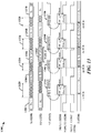
- FIG. 11 is a timing diagram 1100 illustrating the operation of the CDR circuit 1008 under typical operating conditions.
- the CDR circuit 1008 may be used with a variety of multi-wire interfaces, including interfaces that use N ! encoding, N -phase encoding, and other encoding schemes that use symbol transition clocking, including interfaces that employ single-ended multi-wire communication links.
- the CDR circuit 1008 may be configured to extract a clock and data symbols from the spread signal received over the four wires or conductors 1002.
- the spread signal may be defined by a plurality of transition signals including a first signal over a first line interface, conductor, or wire.
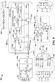
- the CDR circuit 1008 may include a comparator 1010, a set-reset latch 1014, a first analog delay device S 1018, a second analog delay device T 1022, and a level latch 1028.
- a clock extraction circuit 1009 may be defined by the comparator 1010, a set-reset latch 1014, and a first analog delay device S 1018.
- the clock extraction circuit 1009 may be adapted to extract a signal that may be used to obtain a clock signal from state transitions within the received first signal.
- a level latch 1028 receives the first instance of the first signal (SI) 1030 and provides the delayed second instance of the first signal (SD) 1032 to the comparator 1010.
- the level latch 1028 is triggered by a delayed instance of the NE signal 1012.
- a flip-flop device 1026 may also receive the delayed second instance of the first signal (SD) 1032 and outputs a symbol (S) 1034 triggered by the NEFLT signal 1016. That is, the flip-flop device 1026 is triggered by a rising edge on the NEFLT signal 1016. Consequently, the level latch 1028 and second analog delay device 1022 serve to generate the NE signal 1012. In turn, the NE signal 1012 serves to generate the NEFLT signal 1016 which serves as a latching clock for the flip-flop device 1026.
- the NEFLT signal 1016 transitions to a high state in response to the rising edge of the NE signal 1012, and the NEFLT signal 1016 transitions to a low state in response to the rising edge of the NEFLTD signal 1020 after a delay attributable to the first analog delay device S 1018.
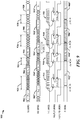
- one or more intermediate or indeterminate states 1120, 1124, 1126, 1128 may occur on the SI signal 1030 due to inter-wire skew, signal overshoot, signal undershoot, crosstalk, and so on.
- the intermediate states on the SI signal 1030 may be regarded as invalid data, and these intermediate states may cause spikes 1144, 1146, 1148, and 1150 in the NE signal 1012 as the output of the comparator 1010 returns towards a low state for short periods of time.
- the spikes 1144, 1146, 1148, and 1150 do not affect the NEFLT signal 1016 output by the set-reset latch 1014.
- the set-reset latch 1014 effectively blocks and/or filters out the spikes 1144, 1146, 1148, and 1150 on the NE signal 1012 from the NEFLT signal 1016.
- the second CDR circuit 1008 in FIG. 10 provides a wider and/or more stable symbols within the SD signal 1032.
- a stable version of the delayed second instance of the first signal (SD signal 1032) can be latched in more quickly, resulting in a stable wider symbol.
- a symbol S1 906' may have a width A in the SD signal 832 while in FIG. 11 the corresponding symbol S1 1106' may have a width B in the SD signal 1032, where width B > width A. Since the stable symbol portion of the SD signal 1032 is wider in this approach, this provides a wider sampling margin so a faster transmission link may be possible relative to the approach in FIGS. 8 and 9 .
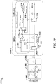
- a level latch 1228 receives the first instance of the first signal (SI) 1230 and provides the delayed second instance of the first signal (SD) 1232.
- the level latch 1228 is triggered by the resulting output NEFLT_COMP 1236 of an OR gate 1222 which has the NEFLT 1216 and NEFLTD signal 1220 as inputs.
- the state of the SI signal 1230 begins to change.
- the NE signal 1212 transitions high when the comparator 1210 first detects a difference between the SI signal 1230 and the SD signal 1232, causing the set-reset latch 1214 to be asynchronously set. Accordingly, the NEFLT signal 1216 transitions high, and this high state is maintained until the set-reset latch 1214 is reset when the NEFLTD signal 1220 becomes high.
- this third CDR circuit 1208 is implemented without the second analog delay device T while still providing wider or more stable symbols within the SD signal 1232 in relation to the approaches in FIG. 8 and FIG. 10 .
- the CDR circuit 1208 of FIG. 12 is a way to achieve minimum delay while guaranteeing to sample valid data in order to output symbol (S) 1234.
- the CDR circuit 1008 of FIG. 10 has no way to make the delay T (i.e., second analog delay device T 1022) as small as the delay (i.e., the delay caused by the OR gate 1222) in FIG. 12 since delay T in FIG. 10 must have a safety margin to account for delay variations due to variations in manufacturing processes, electrical path lengths, temperature, etc.
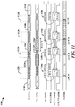
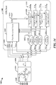
- FIGS. 8 , 10 , and 11 Various examples of the clock extraction circuit 1410 are found in FIGS. 8 , 10 , and 11 , where the NEFLT signal 816, 1016, and/or 1216 may serve as a clock signal.
- a negative hold time logic circuit 1426 may be adapted to sample the delayed second instance of the first signal SD[a] 1432 based on the clock signal and provide a symbol output S[a] 1434.
- the negative hold time logic circuit 1426 includes a separate negative hold time logic device for each of the plurality of line interfaces, each separate negative hold time logic device may be adapted to concurrently sample a delayed instance of a distinct signal SD[a], SD[b], SD[c], ..., SD[n] based on the clock/trigger signal 1414 and provide distinct symbol outputs S[a], S[b], S[c], ..., S[n].
- FIG. 15 illustrates a method for clock and data recovery.
- a spread signal may be received distributed over the plurality of line interfaces, the spread signal carrying symbols with guaranteed symbol-to-symbol state transitions between consecutive symbols, the spread signal defined by a plurality of transition signals including a first signal over a first line interface 1502.
- the first signal may be a differential signal or a single-ended signal.
- the spread signal may be one of a N -factorial ( N! ) encoded signal, a three-phase encoded signal, and/or a N -phase encoded signal.
- obtaining a clock signal may include: (a) comparing the first instance of the first signal (SI) and the delayed instance of the first signal (SD) to provide a comparison signal (NE); (b) latching the comparison signal (NE) to obtain a filtered version of the comparison signal (NEFLT); and/or (c) delaying the filtered version of the comparison signal (NEFLT) to provide a delayed filtered version of the comparison signal (NEFLTD), where the delayed filtered version of the comparison signal (NEFLTD) serves to latch the comparison signal (NE).
- the method may further include capturing the first instance of the first signal to obtain the delayed second instance of the first signal while either the filtered version of the comparison signal (NEFLT) or the delayed filtered version of the comparison signal (NEFLTD) is in a logical high state.
- NEFLT filtered version of the comparison signal
- NEFLTD delayed filtered version of the comparison signal
Landscapes
- Engineering & Computer Science (AREA)
- Computer Networks & Wireless Communication (AREA)
- Signal Processing (AREA)
- Theoretical Computer Science (AREA)
- General Engineering & Computer Science (AREA)
- Power Engineering (AREA)
- Physics & Mathematics (AREA)
- General Physics & Mathematics (AREA)
- Computer Hardware Design (AREA)
- Dc Digital Transmission (AREA)
- Synchronisation In Digital Transmission Systems (AREA)
Claims (15)
- Ein Verfahren, das auf einer Empfängerschaltung betreibbar ist, das Folgendes aufweist:Empfangen eines gespreizten Signals, das über eine Vielzahl von Leitungsschnittstellen verteilt ist, wobei das gespreizte Signal Symbole mit garantierten Symbol-zu-Symbol-Zustandsübergängen zwischen aufeinanderfolgenden Symbolen trägt, wobei das gespreizte Signal durch eine Vielzahl von Zustandsübergangssignalen definiert wird, die ein erstes Signal über eine erste Leitungsschnittstelle und ein zweites Signal über eine zweite Leitungsschnittstelle beinhalten;Erlangen eines Taktsignals basierend auf einem Vergleich von Übergängen zwischen einer ersten Instanz des ersten Signals und einer verzögerten zweiten Instanz des ersten Signals, und einem Vergleich von Übergängen zwischen einer ersten Instanz des zweiten Signals und einer verzögerten zweiten Instanz des zweiten Signals; undSamplen bzw. Abtasten der verzögerten zweiten Instanz des ersten Signals basierend auf dem Taktsignal, um eine Symbolausgabe vorzusehen.
- Verfahren nach Anspruch 1, wobei das erste Signal ein differenzielles Signal ist.
- Verfahren nach Anspruch 1, wobei das erste Signal ein unsymmetrisches Signal bzw. Single-Ended-Signal ist.
- Verfahren nach Anspruch 1, wobei das gespreizte Signal eines von einem N-faktoriell (N!) codierten Signal, einem dreiphasigen codierten Signal oder einem N-phasigen codierten Signal mit drei oder mehr Phasen ist.
- Verfahren nach Anspruch 1, wobei das Abtasten der verzögerten zweiten Instanz des ersten Signals unter Nutzung einer Logikschaltung mit negativer Haltezeit durchgeführt wird.
- Verfahren nach Anspruch 1, wobei das erste Signal und das zweite Signal gleichzeitige Signale sind, die über unterschiedliche Leitungsschnittstellen empfangen werden.
- Verfahren nach Anspruch 1, das weiter Folgendes aufweist:
gleichzeitiges Abtasten einer verzögerten Instanz einer Vielzahl von unterschiedlichen Signalen innerhalb der Vielzahl von Zustandsübergangssignalen basierend auf dem Taktsignal zum Vorsehen distinkter bzw. unterschiedlicher Symbolausgaben. - Verfahren nach Anspruch 1, wobei das Erlangen des Taktsignals Folgendes aufweist:Vergleichen der ersten Instanz des ersten Signals (SI) und der verzögerten zweiten Instanz des ersten Signals (SD) zum Vorsehen eines Vergleichssignals (NE);Latchen bzw. Halten des Vergleichssignals (NE) zum Erlangen einer gefilterten Version des Vergleichssignals (NEFLT); undVerzögern der gefilterten Version des Vergleichssignals (NEFLT) zum Vorsehen einer verzögerten gefilterten Version des Vergleichssignals (NEFLTD), wobei die verzögerte gefilterte Version des Vergleichssignals (NEFLTD) dazu dient, das Vergleichssignal (NE) zu halten.
- Verfahren nach Anspruch 8, das weiter Folgendes aufweist:
Verzögern der ersten Instanz des ersten Signals zum Erlangen der verzögerten zweiten Instanz des ersten Signals. - Verfahren nach Anspruch 8, das weiter Folgendes aufweist:Erfassen der ersten Instanz des ersten Signals zum Erlangen der verzögerten zweiten Instanz des ersten Signals; undVerzögern des Vergleichssignals (NE) unter Nutzung des verzögerten Vergleichssignals (NED) zum Auslösen des Verriegelns des Vergleichssignals (NE).
- Verfahren nach Anspruch 8, das weiter Folgendes aufweist:
Erfassen der ersten Instanz des ersten Signals zum Erlangen der verzögerten zweiten Instanz des ersten Signals, während entweder die gefilterte Version des Vergleichssignals (NEFLT) oder die verzögerte gefilterte Version des Vergleichssignals (NEFLTD) in einem Logisch-Hoch-Zustand ist. - Eine Empfängerschaltung (800, 1000, 1200, 1400), die Folgendes aufweist:Mittel zum Empfangen (806, 1006, 1206, 1406) eines gespreizten Signals, das über eine Vielzahl von Leitungsschnittstellen verteilt ist, wobei das gespreizte Signal Symbole mit garantierten Symbol-zu-Symbol-Zustandsübergängen zwischen aufeinanderfolgenden Symbolen trägt, wobei das gespreizte Signal durch eine Vielzahl von Zustandsübergangssignalen definiert wird, die ein erstes Signal über eine erste Leitungsschnittstelle und ein zweites Signal über eine zweite Leitungsschnittstelle beinhalten;Mittel zum Erlangen (809, 1009, 1209, 1408) eines Taktsignals basierend auf einem Vergleich von Übergängen zwischen einer ersten Instanz des ersten Signals und einer verzögerten zweiten Instanz des ersten Signals, und einem Vergleich von Übergängen zwischen einer ersten Instanz des zweiten Signals und einer verzögerten zweiten Instanz des zweiten Signals; undMittel zum Samplen bzw. Abtasten (826, 1026, 1226, 1426) der verzögerten zweiten Instanz des ersten Signals basierend auf dem Taktsignal, um eine Symbolausgabe vorzusehen.
- Empfängerschaltung nach Anspruch 12, wobei das erste Signal und das zweite Signal gleichzeitige Signale sind, die über unterschiedliche Leitungsschnittstellen empfangen werden.
- Empfängerschaltung nach Anspruch 12, die weiter Folgendes aufweist:
Mittel zum gleichzeitigen Abtasten einer verzögerten Instanz einer Vielzahl von distinkten bzw. unterschiedlichen Signalen innerhalb der Vielzahl von Zustandsübergangssignalen basierend auf dem Taktsignal, um distinkte bzw. unterschiedliche Symbolausgaben vorzusehen. - Empfängerschaltung nach Anspruch 12, wobei die Mittel zum Erlangen des Taktsignals Folgendes aufweisen:Mittel zum Vergleichen der ersten Instanz des ersten Signals (SI) und der verzögerten zweiten Instanz des ersten Signals (SD) zum Vorsehen eines Vergleichssignals (NE);Mittel zum Latchen bzw. Halten des Vergleichssignals (NE) zum Erlangen einer gefilterten Version des Vergleichssignals (NEFLT); undMittel zum Verzögern der gefilterten Version des Vergleichssignals (NEFLT) zum Vorsehen einer verzögerten gefilterten Version des Vergleichssignals (NEFLTD), wobei die verzögerte gefilterte Version des Vergleichssignals (NEFLTD) dazu dient, das Vergleichssignal (NE) zu halten.
Applications Claiming Priority (5)
| Application Number | Priority Date | Filing Date | Title |
|---|---|---|---|
| US14/199,322 US9363071B2 (en) | 2013-03-07 | 2014-03-06 | Circuit to recover a clock signal from multiple wire data signals that changes state every state cycle and is immune to data inter-lane skew as well as data state transition glitches |
| US14/220,056 US9374216B2 (en) | 2013-03-20 | 2014-03-19 | Multi-wire open-drain link with data symbol transition based clocking |
| US14/252,450 US9178690B2 (en) | 2013-10-03 | 2014-04-14 | N factorial dual data rate clock and data recovery |
| US14/459,132 US9313058B2 (en) | 2013-03-07 | 2014-08-13 | Compact and fast N-factorial single data rate clock and data recovery circuits |
| PCT/US2014/065169 WO2015134071A1 (en) | 2014-03-06 | 2014-11-12 | Clock recovery circuit for multiple wire data signals |
Publications (2)
| Publication Number | Publication Date |
|---|---|
| EP3114792A1 EP3114792A1 (de) | 2017-01-11 |
| EP3114792B1 true EP3114792B1 (de) | 2021-06-09 |
Family
ID=54055706
Family Applications (1)
| Application Number | Title | Priority Date | Filing Date |
|---|---|---|---|
| EP14815119.4A Active EP3114792B1 (de) | 2014-03-06 | 2014-11-12 | Schaltung zur wiedergewinnung eines taktsignales von signalen über mehrere drähte |
Country Status (6)
| Country | Link |
|---|---|
| EP (1) | EP3114792B1 (de) |
| JP (1) | JP6219538B2 (de) |
| KR (1) | KR101688377B1 (de) |
| CN (1) | CN106063181B (de) |
| ES (1) | ES2881302T3 (de) |
| WO (1) | WO2015134071A1 (de) |
Families Citing this family (7)
| Publication number | Priority date | Publication date | Assignee | Title |
|---|---|---|---|---|
| JP2018534847A (ja) * | 2015-10-05 | 2018-11-22 | クゥアルコム・インコーポレイテッドQualcomm Incorporated | マルチレーンn階乗符号化通信システムおよび他のマルチワイヤ通信システム |
| US10628625B2 (en) * | 2016-04-08 | 2020-04-21 | Synopsys, Inc. | Incrementally distributing logical wires onto physical sockets by reducing critical path delay |
| KR102629185B1 (ko) * | 2016-12-07 | 2024-01-24 | 에스케이하이닉스 주식회사 | 데이터 통신을 위한 수신기 |
| FR3102268B1 (fr) * | 2019-10-18 | 2023-03-10 | St Microelectronics Rousset | Procédé d’authentification d’un circuit sur puce et système sur puce associé |
| CN113676992B (zh) * | 2020-05-13 | 2022-11-25 | 华为技术有限公司 | 时钟信号同步方法及设备 |
| KR20220071985A (ko) | 2020-11-23 | 2022-06-02 | 한국전자기술연구원 | 비제로복귀 및 펄스진폭변조를 지원하는 듀얼모드 클록 데이터 복원 회로 및 방법 |
| CN113395414B (zh) * | 2021-06-15 | 2022-11-11 | 杭州海康机器人股份有限公司 | 波形恢复电路和工业相机 |
Family Cites Families (16)
| Publication number | Priority date | Publication date | Assignee | Title |
|---|---|---|---|---|
| DE3329773A1 (de) * | 1983-08-18 | 1985-02-28 | Siemens AG, 1000 Berlin und 8000 München | Verfahren und anordnung zur zeitgleichen flankenanpassung mehrerer taktsynchroner datenfluesse |
| US5493538A (en) * | 1994-11-14 | 1996-02-20 | Texas Instruments Incorporated | Minimum pulse width address transition detection circuit |
| US6731000B1 (en) * | 2002-11-12 | 2004-05-04 | Koninklijke Philips Electronics N.V. | Folded-flex bondwire-less multichip power package |
| JP4604627B2 (ja) * | 2004-09-22 | 2011-01-05 | ソニー株式会社 | エンコーダ装置およびデコーダ装置 |
| US7692563B2 (en) * | 2006-04-27 | 2010-04-06 | Panasonic Corporation | Multiple differential transmission system including signal transmitter and signal receiver connected via three signal lines |
| CN101083472B (zh) * | 2006-05-30 | 2011-07-20 | 富士通株式会社 | 对施加给信号的补偿进行不对称调节的系统及方法 |
| US7881415B2 (en) * | 2006-12-29 | 2011-02-01 | Atmel Corporation | Communication protocol method and apparatus for a single wire device |
| US9711041B2 (en) * | 2012-03-16 | 2017-07-18 | Qualcomm Incorporated | N-phase polarity data transfer |
| US8064535B2 (en) | 2007-03-02 | 2011-11-22 | Qualcomm Incorporated | Three phase and polarity encoded serial interface |
| GB2456517A (en) * | 2008-01-15 | 2009-07-22 | Andrzej Radecki | Serial data communication circuit for use with transmission lines using both data and clock to enable recovery of data synchronously |
| US20090243681A1 (en) * | 2008-03-26 | 2009-10-01 | Rambus Inc. | Embedded Source-Synchronous Clock Signals |
| KR101061989B1 (ko) * | 2008-12-03 | 2011-09-05 | (주)신창코넥타 | 스페이서 및 그 스페이서를 포함하는 차량용 클럭 스프링 장치 |
| JP5503207B2 (ja) * | 2009-07-22 | 2014-05-28 | ザインエレクトロニクス株式会社 | 送信機および通信システム |
| US8077063B2 (en) * | 2010-01-18 | 2011-12-13 | Freescale Semiconductor, Inc. | Method and system for determining bit stream zone statistics |
| US9363071B2 (en) * | 2013-03-07 | 2016-06-07 | Qualcomm Incorporated | Circuit to recover a clock signal from multiple wire data signals that changes state every state cycle and is immune to data inter-lane skew as well as data state transition glitches |
| US9178690B2 (en) * | 2013-10-03 | 2015-11-03 | Qualcomm Incorporated | N factorial dual data rate clock and data recovery |
-
2014
- 2014-11-12 EP EP14815119.4A patent/EP3114792B1/de active Active
- 2014-11-12 WO PCT/US2014/065169 patent/WO2015134071A1/en not_active Ceased
- 2014-11-12 KR KR1020167024472A patent/KR101688377B1/ko not_active Expired - Fee Related
- 2014-11-12 CN CN201480076817.5A patent/CN106063181B/zh active Active
- 2014-11-12 ES ES14815119T patent/ES2881302T3/es active Active
- 2014-11-12 JP JP2016555330A patent/JP6219538B2/ja active Active
Non-Patent Citations (1)
| Title |
|---|
| None * |
Also Published As
| Publication number | Publication date |
|---|---|
| EP3114792A1 (de) | 2017-01-11 |
| KR20160113721A (ko) | 2016-09-30 |
| ES2881302T3 (es) | 2021-11-29 |
| WO2015134071A1 (en) | 2015-09-11 |
| CN106063181A (zh) | 2016-10-26 |
| JP6219538B2 (ja) | 2017-10-25 |
| JP2017512436A (ja) | 2017-05-18 |
| CN106063181B (zh) | 2018-03-13 |
| KR101688377B1 (ko) | 2017-01-02 |
Similar Documents
| Publication | Publication Date | Title |
|---|---|---|
| US9313058B2 (en) | Compact and fast N-factorial single data rate clock and data recovery circuits | |
| US9998300B2 (en) | N-phase phase and polarity encoded serial interface | |
| EP3114792B1 (de) | Schaltung zur wiedergewinnung eines taktsignales von signalen über mehrere drähte | |
| US9148198B1 (en) | Programmable pre-emphasis circuit for MIPI C-PHY | |
| TWI720008B (zh) | 用於三相介面之多相位時脈資料回復 | |
| EP3053296B1 (de) | N factorisierte takt- und daten-rückgewinnung mit doppelter rate | |
| US9203599B2 (en) | Multi-lane N-factorial (N!) and other multi-wire communication systems | |
| US9735948B2 (en) | Multi-lane N-factorial (N!) and other multi-wire communication systems | |
| CN114616793A (zh) | 用于高速下一代c-phy的小环路延迟时钟和数据恢复块 | |
| CN114631291B (zh) | C-phy半速率线状态编码器和解码器 | |
| CN115462039B (zh) | C-phy接口中的单位间隔抖动改进 | |
| WO2025054011A1 (en) | Radio frequency interference common mode injection in a c-phy receiver | |
| TWI822732B (zh) | 獨立配對的3相眼圖取樣電路 | |
| KR102265187B1 (ko) | 클럭 복구 회로 | |
| KR102520096B1 (ko) | 인코딩된 멀티-레인 n-팩토리얼 및 다른 멀티-와이어 통신 시스템들 | |
| KR20260062934A (ko) | C-phy 수신기에서의 라디오 주파수 간섭 공통 모드 주입 |
Legal Events
| Date | Code | Title | Description |
|---|---|---|---|
| PUAI | Public reference made under article 153(3) epc to a published international application that has entered the european phase |
Free format text: ORIGINAL CODE: 0009012 |
|
| STAA | Information on the status of an ep patent application or granted ep patent |
Free format text: STATUS: REQUEST FOR EXAMINATION WAS MADE |
|
| 17P | Request for examination filed |
Effective date: 20160728 |
|
| AK | Designated contracting states |
Kind code of ref document: A1 Designated state(s): AL AT BE BG CH CY CZ DE DK EE ES FI FR GB GR HR HU IE IS IT LI LT LU LV MC MK MT NL NO PL PT RO RS SE SI SK SM TR |
|
| AX | Request for extension of the european patent |
Extension state: BA ME |
|
| DAX | Request for extension of the european patent (deleted) | ||
| STAA | Information on the status of an ep patent application or granted ep patent |
Free format text: STATUS: EXAMINATION IS IN PROGRESS |
|
| 17Q | First examination report despatched |
Effective date: 20190903 |
|
| GRAP | Despatch of communication of intention to grant a patent |
Free format text: ORIGINAL CODE: EPIDOSNIGR1 |
|
| STAA | Information on the status of an ep patent application or granted ep patent |
Free format text: STATUS: GRANT OF PATENT IS INTENDED |
|
| INTG | Intention to grant announced |
Effective date: 20201007 |
|
| GRAJ | Information related to disapproval of communication of intention to grant by the applicant or resumption of examination proceedings by the epo deleted |
Free format text: ORIGINAL CODE: EPIDOSDIGR1 |
|
| STAA | Information on the status of an ep patent application or granted ep patent |
Free format text: STATUS: EXAMINATION IS IN PROGRESS |
|
| GRAP | Despatch of communication of intention to grant a patent |
Free format text: ORIGINAL CODE: EPIDOSNIGR1 |
|
| STAA | Information on the status of an ep patent application or granted ep patent |
Free format text: STATUS: GRANT OF PATENT IS INTENDED |
|
| INTC | Intention to grant announced (deleted) | ||
| INTG | Intention to grant announced |
Effective date: 20210305 |
|
| GRAS | Grant fee paid |
Free format text: ORIGINAL CODE: EPIDOSNIGR3 |
|
| GRAA | (expected) grant |
Free format text: ORIGINAL CODE: 0009210 |
|
| STAA | Information on the status of an ep patent application or granted ep patent |
Free format text: STATUS: THE PATENT HAS BEEN GRANTED |
|
| AK | Designated contracting states |
Kind code of ref document: B1 Designated state(s): AL AT BE BG CH CY CZ DE DK EE ES FI FR GB GR HR HU IE IS IT LI LT LU LV MC MK MT NL NO PL PT RO RS SE SI SK SM TR |
|
| REG | Reference to a national code |
Ref country code: GB Ref legal event code: FG4D |
|
| REG | Reference to a national code |
Ref country code: CH Ref legal event code: EP Ref country code: AT Ref legal event code: REF Ref document number: 1401372 Country of ref document: AT Kind code of ref document: T Effective date: 20210615 |
|
| REG | Reference to a national code |
Ref country code: DE Ref legal event code: R096 Ref document number: 602014078046 Country of ref document: DE |
|
| REG | Reference to a national code |
Ref country code: IE Ref legal event code: FG4D |
|
| PGFP | Annual fee paid to national office [announced via postgrant information from national office to epo] |
Ref country code: NL Payment date: 20210609 Year of fee payment: 8 |
|
| REG | Reference to a national code |
Ref country code: SE Ref legal event code: TRGR |
|
| REG | Reference to a national code |
Ref country code: LT Ref legal event code: MG9D |
|
| REG | Reference to a national code |
Ref country code: NO Ref legal event code: T2 Effective date: 20210609 |
|
| PG25 | Lapsed in a contracting state [announced via postgrant information from national office to epo] |
Ref country code: BG Free format text: LAPSE BECAUSE OF FAILURE TO SUBMIT A TRANSLATION OF THE DESCRIPTION OR TO PAY THE FEE WITHIN THE PRESCRIBED TIME-LIMIT Effective date: 20210909 Ref country code: FI Free format text: LAPSE BECAUSE OF FAILURE TO SUBMIT A TRANSLATION OF THE DESCRIPTION OR TO PAY THE FEE WITHIN THE PRESCRIBED TIME-LIMIT Effective date: 20210609 Ref country code: LT Free format text: LAPSE BECAUSE OF FAILURE TO SUBMIT A TRANSLATION OF THE DESCRIPTION OR TO PAY THE FEE WITHIN THE PRESCRIBED TIME-LIMIT Effective date: 20210609 Ref country code: HR Free format text: LAPSE BECAUSE OF FAILURE TO SUBMIT A TRANSLATION OF THE DESCRIPTION OR TO PAY THE FEE WITHIN THE PRESCRIBED TIME-LIMIT Effective date: 20210609 |
|
| REG | Reference to a national code |
Ref country code: AT Ref legal event code: MK05 Ref document number: 1401372 Country of ref document: AT Kind code of ref document: T Effective date: 20210609 |
|
| REG | Reference to a national code |
Ref country code: ES Ref legal event code: FG2A Ref document number: 2881302 Country of ref document: ES Kind code of ref document: T3 Effective date: 20211129 |
|
| PG25 | Lapsed in a contracting state [announced via postgrant information from national office to epo] |
Ref country code: RS Free format text: LAPSE BECAUSE OF FAILURE TO SUBMIT A TRANSLATION OF THE DESCRIPTION OR TO PAY THE FEE WITHIN THE PRESCRIBED TIME-LIMIT Effective date: 20210609 Ref country code: LV Free format text: LAPSE BECAUSE OF FAILURE TO SUBMIT A TRANSLATION OF THE DESCRIPTION OR TO PAY THE FEE WITHIN THE PRESCRIBED TIME-LIMIT Effective date: 20210609 Ref country code: GR Free format text: LAPSE BECAUSE OF FAILURE TO SUBMIT A TRANSLATION OF THE DESCRIPTION OR TO PAY THE FEE WITHIN THE PRESCRIBED TIME-LIMIT Effective date: 20210910 |
|
| PG25 | Lapsed in a contracting state [announced via postgrant information from national office to epo] |
Ref country code: PT Free format text: LAPSE BECAUSE OF FAILURE TO SUBMIT A TRANSLATION OF THE DESCRIPTION OR TO PAY THE FEE WITHIN THE PRESCRIBED TIME-LIMIT Effective date: 20211011 Ref country code: RO Free format text: LAPSE BECAUSE OF FAILURE TO SUBMIT A TRANSLATION OF THE DESCRIPTION OR TO PAY THE FEE WITHIN THE PRESCRIBED TIME-LIMIT Effective date: 20210609 Ref country code: AT Free format text: LAPSE BECAUSE OF FAILURE TO SUBMIT A TRANSLATION OF THE DESCRIPTION OR TO PAY THE FEE WITHIN THE PRESCRIBED TIME-LIMIT Effective date: 20210609 Ref country code: SM Free format text: LAPSE BECAUSE OF FAILURE TO SUBMIT A TRANSLATION OF THE DESCRIPTION OR TO PAY THE FEE WITHIN THE PRESCRIBED TIME-LIMIT Effective date: 20210609 Ref country code: SK Free format text: LAPSE BECAUSE OF FAILURE TO SUBMIT A TRANSLATION OF THE DESCRIPTION OR TO PAY THE FEE WITHIN THE PRESCRIBED TIME-LIMIT Effective date: 20210609 Ref country code: EE Free format text: LAPSE BECAUSE OF FAILURE TO SUBMIT A TRANSLATION OF THE DESCRIPTION OR TO PAY THE FEE WITHIN THE PRESCRIBED TIME-LIMIT Effective date: 20210609 Ref country code: CZ Free format text: LAPSE BECAUSE OF FAILURE TO SUBMIT A TRANSLATION OF THE DESCRIPTION OR TO PAY THE FEE WITHIN THE PRESCRIBED TIME-LIMIT Effective date: 20210609 |
|
| PG25 | Lapsed in a contracting state [announced via postgrant information from national office to epo] |
Ref country code: PL Free format text: LAPSE BECAUSE OF FAILURE TO SUBMIT A TRANSLATION OF THE DESCRIPTION OR TO PAY THE FEE WITHIN THE PRESCRIBED TIME-LIMIT Effective date: 20210609 |
|
| REG | Reference to a national code |
Ref country code: DE Ref legal event code: R097 Ref document number: 602014078046 Country of ref document: DE |
|
| PLBE | No opposition filed within time limit |
Free format text: ORIGINAL CODE: 0009261 |
|
| STAA | Information on the status of an ep patent application or granted ep patent |
Free format text: STATUS: NO OPPOSITION FILED WITHIN TIME LIMIT |
|
| PG25 | Lapsed in a contracting state [announced via postgrant information from national office to epo] |
Ref country code: DK Free format text: LAPSE BECAUSE OF FAILURE TO SUBMIT A TRANSLATION OF THE DESCRIPTION OR TO PAY THE FEE WITHIN THE PRESCRIBED TIME-LIMIT Effective date: 20210609 |
|
| 26N | No opposition filed |
Effective date: 20220310 |
|
| PG25 | Lapsed in a contracting state [announced via postgrant information from national office to epo] |
Ref country code: AL Free format text: LAPSE BECAUSE OF FAILURE TO SUBMIT A TRANSLATION OF THE DESCRIPTION OR TO PAY THE FEE WITHIN THE PRESCRIBED TIME-LIMIT Effective date: 20210609 |
|
| PG25 | Lapsed in a contracting state [announced via postgrant information from national office to epo] |
Ref country code: MC Free format text: LAPSE BECAUSE OF FAILURE TO SUBMIT A TRANSLATION OF THE DESCRIPTION OR TO PAY THE FEE WITHIN THE PRESCRIBED TIME-LIMIT Effective date: 20210609 |
|
| PG25 | Lapsed in a contracting state [announced via postgrant information from national office to epo] |
Ref country code: LU Free format text: LAPSE BECAUSE OF NON-PAYMENT OF DUE FEES Effective date: 20211112 Ref country code: IT Free format text: LAPSE BECAUSE OF FAILURE TO SUBMIT A TRANSLATION OF THE DESCRIPTION OR TO PAY THE FEE WITHIN THE PRESCRIBED TIME-LIMIT Effective date: 20210609 Ref country code: BE Free format text: LAPSE BECAUSE OF NON-PAYMENT OF DUE FEES Effective date: 20211130 |
|
| REG | Reference to a national code |
Ref country code: BE Ref legal event code: MM Effective date: 20211130 |
|
| PG25 | Lapsed in a contracting state [announced via postgrant information from national office to epo] |
Ref country code: IE Free format text: LAPSE BECAUSE OF NON-PAYMENT OF DUE FEES Effective date: 20211112 |
|
| PG25 | Lapsed in a contracting state [announced via postgrant information from national office to epo] |
Ref country code: HU Free format text: LAPSE BECAUSE OF FAILURE TO SUBMIT A TRANSLATION OF THE DESCRIPTION OR TO PAY THE FEE WITHIN THE PRESCRIBED TIME-LIMIT; INVALID AB INITIO Effective date: 20141112 |
|
| PG25 | Lapsed in a contracting state [announced via postgrant information from national office to epo] |
Ref country code: CY Free format text: LAPSE BECAUSE OF FAILURE TO SUBMIT A TRANSLATION OF THE DESCRIPTION OR TO PAY THE FEE WITHIN THE PRESCRIBED TIME-LIMIT Effective date: 20210609 |
|
| REG | Reference to a national code |
Ref country code: NL Ref legal event code: MM Effective date: 20221201 |
|
| PG25 | Lapsed in a contracting state [announced via postgrant information from national office to epo] |
Ref country code: NL Free format text: LAPSE BECAUSE OF NON-PAYMENT OF DUE FEES Effective date: 20221201 |
|
| PG25 | Lapsed in a contracting state [announced via postgrant information from national office to epo] |
Ref country code: MK Free format text: LAPSE BECAUSE OF FAILURE TO SUBMIT A TRANSLATION OF THE DESCRIPTION OR TO PAY THE FEE WITHIN THE PRESCRIBED TIME-LIMIT Effective date: 20210609 |
|
| PG25 | Lapsed in a contracting state [announced via postgrant information from national office to epo] |
Ref country code: MT Free format text: LAPSE BECAUSE OF FAILURE TO SUBMIT A TRANSLATION OF THE DESCRIPTION OR TO PAY THE FEE WITHIN THE PRESCRIBED TIME-LIMIT Effective date: 20210609 |
|
| PGFP | Annual fee paid to national office [announced via postgrant information from national office to epo] |
Ref country code: CH Payment date: 20241201 Year of fee payment: 11 |
|
| PG25 | Lapsed in a contracting state [announced via postgrant information from national office to epo] |
Ref country code: TR Free format text: LAPSE BECAUSE OF FAILURE TO SUBMIT A TRANSLATION OF THE DESCRIPTION OR TO PAY THE FEE WITHIN THE PRESCRIBED TIME-LIMIT Effective date: 20210609 |
|
| PGFP | Annual fee paid to national office [announced via postgrant information from national office to epo] |
Ref country code: DE Payment date: 20251013 Year of fee payment: 12 |
|
| PGFP | Annual fee paid to national office [announced via postgrant information from national office to epo] |
Ref country code: GB Payment date: 20251009 Year of fee payment: 12 |
|
| PGFP | Annual fee paid to national office [announced via postgrant information from national office to epo] |
Ref country code: NO Payment date: 20251028 Year of fee payment: 12 |
|
| PGFP | Annual fee paid to national office [announced via postgrant information from national office to epo] |
Ref country code: FR Payment date: 20251013 Year of fee payment: 12 |
|
| PGFP | Annual fee paid to national office [announced via postgrant information from national office to epo] |
Ref country code: SE Payment date: 20251111 Year of fee payment: 12 |
|
| PGFP | Annual fee paid to national office [announced via postgrant information from national office to epo] |
Ref country code: ES Payment date: 20251209 Year of fee payment: 12 |