EP3114792B1 - Clock recovery circuit for multiple wire data signals - Google Patents
Clock recovery circuit for multiple wire data signals Download PDFInfo
- Publication number
- EP3114792B1 EP3114792B1 EP14815119.4A EP14815119A EP3114792B1 EP 3114792 B1 EP3114792 B1 EP 3114792B1 EP 14815119 A EP14815119 A EP 14815119A EP 3114792 B1 EP3114792 B1 EP 3114792B1
- Authority
- EP
- European Patent Office
- Prior art keywords
- signal
- instance
- delayed
- comparison
- symbol
- Prior art date
- Legal status (The legal status is an assumption and is not a legal conclusion. Google has not performed a legal analysis and makes no representation as to the accuracy of the status listed.)
- Active
Links
Images


Classifications
-
- H—ELECTRICITY
- H04—ELECTRIC COMMUNICATION TECHNIQUE
- H04L—TRANSMISSION OF DIGITAL INFORMATION, e.g. TELEGRAPHIC COMMUNICATION
- H04L7/00—Arrangements for synchronising receiver with transmitter
- H04L7/02—Speed or phase control by the received code signals, the signals containing no special synchronisation information
- H04L7/033—Speed or phase control by the received code signals, the signals containing no special synchronisation information using the transitions of the received signal to control the phase of the synchronising-signal-generating means, e.g. using a phase-locked loop
-
- G—PHYSICS
- G06—COMPUTING OR CALCULATING; COUNTING
- G06F—ELECTRIC DIGITAL DATA PROCESSING
- G06F13/00—Interconnection of, or transfer of information or other signals between, memories, input/output devices or central processing units
- G06F13/38—Information transfer, e.g. on bus
- G06F13/40—Bus structure
-
- G—PHYSICS
- G06—COMPUTING OR CALCULATING; COUNTING
- G06F—ELECTRIC DIGITAL DATA PROCESSING
- G06F13/00—Interconnection of, or transfer of information or other signals between, memories, input/output devices or central processing units
- G06F13/38—Information transfer, e.g. on bus
- G06F13/42—Bus transfer protocol, e.g. handshake; Synchronisation
- G06F13/4265—Bus transfer protocol, e.g. handshake; Synchronisation on a point to point bus
- G06F13/4278—Bus transfer protocol, e.g. handshake; Synchronisation on a point to point bus using an embedded synchronisation
-
- H—ELECTRICITY
- H04—ELECTRIC COMMUNICATION TECHNIQUE
- H04L—TRANSMISSION OF DIGITAL INFORMATION, e.g. TELEGRAPHIC COMMUNICATION
- H04L25/00—Baseband systems
- H04L25/02—Details ; arrangements for supplying electrical power along data transmission lines
- H04L25/0264—Arrangements for coupling to transmission lines
- H04L25/0292—Arrangements specific to the receiver end
-
- H—ELECTRICITY
- H04—ELECTRIC COMMUNICATION TECHNIQUE
- H04L—TRANSMISSION OF DIGITAL INFORMATION, e.g. TELEGRAPHIC COMMUNICATION
- H04L25/00—Baseband systems
- H04L25/02—Details ; arrangements for supplying electrical power along data transmission lines
- H04L25/14—Channel dividing arrangements, i.e. in which a single bit stream is divided between several baseband channels and reassembled at the receiver
Definitions
- a receiver circuit may comprise a plurality of line interfaces, a plurality of receivers, a clock extraction circuit, and a negative hold time logic circuit.
- the plurality of line interfaces may be configured to receive a spread signal distributed over the plurality of line interfaces, the spread signal carrying symbols with guaranteed symbol-to-symbol state transitions between consecutive symbols, the spread signal defined by a plurality of state transition signals including a first signal over a first line interface.
- the plurality of receivers may be coupled to the line interfaces.
- the plurality of receivers may be differential receivers and the first signal is a differential signal.
- the plurality of receivers may be single-ended receivers and the first signal is a single-ended signal.
- the spread signal may be one of a N -factorial ( N! ) encoded signal, a three-phase encoded signal, and/or a N -phase encoded signal.
- the clock extraction circuit may be adapted to obtain a clock signal based on a comparison between a first instance of the first signal, and a delayed second instance of the first signal.
- the negative hold time logic circuit may be adapted to sample the delayed second instance of the first signal based on the clock signal and provide a symbol output.
- the negative hold time logic circuit may include a separate negative hold time logic device for each of the plurality of line interfaces, each separate negative hold time logic device adapted to concurrently sample a delayed instance of a distinct received signal, within the plurality of state transition signals, based on the clock signal and provide distinct symbol outputs.
- the receiver circuit may include: (a) a latch device that captures the first instance of the first signal and outputs the delayed second instance of the first signal; and/or (b) a second analog delay device that delays the comparison signal (NE) and uses the delayed comparison signal (NED) to trigger the latch device.
- a latch device that captures the first instance of the first signal and outputs the delayed second instance of the first signal
- a second analog delay device that delays the comparison signal (NE) and uses the delayed comparison signal (NED) to trigger the latch device.
- the method may further include generating the clock signal based on additional comparisons between a first instance of a received second signal, within the plurality of state transition signals, and a delayed second instance of the second signal, where the first signal and the second signal are concurrent signals received over different line interfaces.
- the method may further include concurrently sampling a delayed instance of a plurality of distinct signals, within the plurality of state transition signals, based on the clock signal and provide distinct symbol outputs.
- obtaining a clock signal may include: (a) comparing the first instance of the first signal (SI) and the delayed instance of the first signal (SD) to provide a comparison signal (NE); (b) latching the comparison signal (NE) to obtain a filtered version of the comparison signal (NEFLT); and/or (c) delaying the filtered version of the comparison signal (NEFLT) to provide a delayed filtered version of the comparison signal (NEFLTD), where the delayed filtered version of the comparison signal (NEFLTD) serves to latch the comparison signal (NE).
- the method may further include delaying the first instance of the first signal to obtain the delayed second instance of the first signal.
- the method may further include: (a) capturing the first instance of the first signal to obtain the delayed second instance of the first signal; and/or (b) delaying the comparison signal (NE) and using the delayed comparison signal (NED) to trigger the latching of the comparison signal (NE).
- the method may further include capturing the first instance of the first signal to obtain the delayed second instance of the first signal while either the filtered version of the comparison signal (NEFLT) or the delayed filtered version of the comparison signal (NEFLTD) is in a logical high state.
- the processing circuit 102 may be controlled by one or more of an operating system and an application programming interface (API) 110 layer that supports and enables execution of software modules residing in storage media, such as the memory device 112 of the wireless device.
- the memory device 112 may include read-only memory (ROM) or random-access memory (RAM), electrically erasable programmable ROM (EEPROM), flash cards, or any memory device that can be used in processing systems and computing platforms.
- the processing circuit 102 may include or access a local database 114 that can maintain operational parameters and other information used to configure and operate the apparatus 100.
- the local database 114 may be implemented using one or more of a database module, flash memory, magnetic media, EEPROM, optical media, tape, soft or hard disk, or the like.
- the processing circuit may also be operably coupled to external devices such as an antenna 122, a display 124, operator controls, such as button 128 and keypad 126 among other components.
- the communication link 220 may provide multiple channels 222, 224 and 226.
- One or more channels 226 may be bidirectional, and may operate in half-duplex and/or full-duplex modes.
- One or more channels 222 and 224 may be unidirectional.
- the communication link 220 may be asymmetrical, providing higher bandwidth in one direction.
- a first communications channel 222 may be referred to as a forward link 222 while a second communications channel 224 may be referred to as a reverse link 224.
- the first IC device 202 may be designated as a host system or transmitter, while the second IC device 230 may be designated as a client system or receiver, even if both IC devices 202 and 230 are configured to transmit and receive on the communications link 222.
- the forward link 222 may operate at a higher data rate when communicating data from a first IC device 202 to a second IC device 230, while the reverse link 224 may operate at a lower data rate when communicating data from the second IC device 230 to the first IC device 202.
- the IC devices 202 and 230 may each have a processor or other processing and/or computing circuit or device 206, 236.
- the first IC device 202 may perform core functions of the apparatus 200, including maintaining wireless communications through a wireless transceiver 204 and an antenna 214, while the second IC device 230 may support a user interface that manages or operates a display controller 232.
- the second IC device 230 may be adapted to control operations of a camera or video input device using a camera controller 234.
- Other features supported by one or more of the IC devices 202 and 230 may include a keyboard, a voice-recognition component, and other input or output devices.
- the reverse link 224 may be operated in the same manner as the forward link 222, and the forward link 222 and reverse link 224 may be capable of transmitting at comparable speeds or at different speeds, where speed may be expressed as data transfer rate and/or clocking rates.
- the forward and reverse data rates may be substantially the same or differ by orders of magnitude, depending on the application.
- a single bidirectional link 226 may support communications between the first IC device 202 and the second IC device 230.
- the forward link 222 and/or reverse link 224 may be configurable to operate in a bidirectional mode when, for example, the forward and reverse links 222 and 224 share the same physical connections and operate in a half-duplex manner.
- the communication link 220 may be operated to communicate control, command and other information between the first IC device 202 and the second IC device 230 in accordance with an industry or other standard.
- forward and reverse links 222 and 224 may be configured or adapted to support a wide video graphics array (WVGA) 80 frames per second LCD driver IC without a frame buffer, delivering pixel data at 810 Mbps for display refresh.
- WVGA wide video graphics array
- forward and reverse links 222 and 224 may be configured or adapted to enable communications between with dynamic random access memory (DRAM), such as double data rate synchronous dynamic random access memory (SDRAM).
- DRAM dynamic random access memory
- SDRAM double data rate synchronous dynamic random access memory
- Encoding devices 210 and/or 230 can encode multiple bits per clock transition, and multiple sets of wires can be used to transmit and receive data from the SDRAM, control signals, address signals, and so on.
- the communication link 220 of FIG. 2 may be implemented as a wired bus that includes a plurality of signal wires (denoted as N wires).
- the N wires may be configured to carry data encoded in symbols, where clock information is embedded in a sequence of the symbols transmitted over the plurality of wires. Examples of encoding techniques used with N -wire interfaces include N -factorial ( N! ) encoding, and N -phase encoding.
- the IC devices 202 and/or 230 (and/or components therein) illustrated in FIG. 2 may implement clock and data recovery, according to one or more aspects described herein, to recover a clock embedded within differential signal transitions in a multi-wire (N-Wire) communication system (e.g., N -factorial N ! encoding, and N -phase encoding).
- N-Wire multi-wire
- a clock signal is embedded within this 3-wire differential signaling by guaranteeing that there is a symbol change every cycle.
- a clock data recovery circuit that extracts a clock signal from the differential signal must also minimize jitter. This clock signal may be used to synchronize decoding of the symbols in the 3-wire differential signal. While certain logic circuits may serve to minimize jitter, these require a relatively large number of logic devices, which is a problem when scaling up to n-wire differential signaling.
- the decoder circuit 320 decodes the three differential signals RX AB 314, RX_BC 316, and RX_CA 318 and outputs the six states XM, YM, ZM, ZP, YP, and XP.
- each of the six states XM, YM, ZM, ZP, YP, and XP may represent a symbol, and the encoding used guarantees a symbol-to-symbol state transition for transmitted signals.
- the combination of differential signals RX_AB 314, RX_BC 316, and RX_CA 318 may be referred to a spread signal, where the spread signal carries the symbols. Due to their guaranteed state transitions, each of the differential signals RX_AB 314, RX_BC 316, and RX_CA 318 may be referred to as a state transition signal.
- the receivers 312 are illustrated as differential receivers which take as inputs two signals from two different wires (e.g., AB, BC, AC) and output a differential signal (i.e., the output signal being the difference between the two input signals).
- the voltage difference between two wires/conductors may define a differential signal.
- the current flow direction in each wire/conductor may also be used (alone or in combination with voltage) define a differential signal.
- FIG. 4 is a diagram illustrating an example of N-factorial ( N !) encoding used on an N -wire interface 400 provided between two devices 402 and 420.
- a transcoder 406 may be used to encode data 404 and clock information in symbols to be transmitted over a set of N wires 414.
- the clock information may be derived from a transmit clock 412 and may be encoded in a sequence of symbols transmitted in N C 2 differential signals over the N wires 414 by ensuring that a signaling state transition occurs on at least one of the N C 2 signals between consecutive symbols.
- the principles and techniques disclosed for 3-wire, 3-phase encoders can be applied in other configurations of M-wire, N -phase polarity encoders.
- phase state for each conductor 510a, 510b, 510c may be determined by voltage difference between the conductor 510a, 510b or 510c and at least one other conductor 510a, 510b and/or 510c, or by the direction of current flow, or lack of current flow, in the conductor 510a, 510b or 510c.
- state transition diagram 550 three phase states (S 1 , S 2 and S 3 ) are defined.
- a logic 1 may be encoded when the three wires 510a, 510b, 510c transition from phase state S 1 to phase state S 2 and a logic 0 may be encoded when the three wires 510a, 510b, 510c transition from phase state S 1 to phase state S 3 .
- direction of rotation may be easily determined based on which of the three wires 510a, 510b, 510c is undriven before and after the transition.
- one polarity encoding state may be determined by the current flow between the first and second conductors 510a, 510b, 510c or the voltage polarities of the first and second conductors 510a, 510b, 510c.
- two bits of data may be encoded at each phase transition.
- a decoder may determine the direction of signal phase rotation to obtain the first bit, and the second bit may be determined based on the polarity difference between two of the signals 602,604 and 606.
- one or more intermediate or indeterminate states 920, 924, 926, 928 may occur on the SI signal 830 due to inter-wire skew, signal overshoot, signal undershoot, crosstalk, and so on.
- the intermediate states on SI 830 may be regarded as invalid data, and these intermediate states may cause spikes 944, 946, 948, and 950 in the NE signal 812 as the output of the comparator 810 returns towards a low state for short periods of time.
- the spikes 944, 946, 948, and 950 do not affect the NEFLT signal 816 output by the set-reset latch 814.
- the set-reset latch 814 effectively blocks and/or filters out the spikes 944, 946, 948, and 950 on the NE signal 812 from the NEFLT signal 816.
- the flip-flop device 826 may have a negative hold time (-ht) as the input symbols 902, 904, 906, 908, and 910 in the SI signal 830 can change prior to the symbol being latched or captured by the flip-flop device 826.
- a negative hold time (-ht)
- each symbol 902', 904', 906' and 908' in the SD signal 832 is set or captured by the flip-flop device 826 at the rising clock edge of the NEFLT signal 816, which occurs after the input symbols 902, 904, 906, 908, and 910 have changed in the SI signal 830.
- FIG. 11 is a timing diagram 1100 illustrating the operation of the CDR circuit 1008 under typical operating conditions.
- the CDR circuit 1008 may be used with a variety of multi-wire interfaces, including interfaces that use N ! encoding, N -phase encoding, and other encoding schemes that use symbol transition clocking, including interfaces that employ single-ended multi-wire communication links.
- the CDR circuit 1008 may be configured to extract a clock and data symbols from the spread signal received over the four wires or conductors 1002.
- the spread signal may be defined by a plurality of transition signals including a first signal over a first line interface, conductor, or wire.
- the CDR circuit 1008 may include a comparator 1010, a set-reset latch 1014, a first analog delay device S 1018, a second analog delay device T 1022, and a level latch 1028.
- a clock extraction circuit 1009 may be defined by the comparator 1010, a set-reset latch 1014, and a first analog delay device S 1018.
- the clock extraction circuit 1009 may be adapted to extract a signal that may be used to obtain a clock signal from state transitions within the received first signal.
- a level latch 1028 receives the first instance of the first signal (SI) 1030 and provides the delayed second instance of the first signal (SD) 1032 to the comparator 1010.
- the level latch 1028 is triggered by a delayed instance of the NE signal 1012.
- a flip-flop device 1026 may also receive the delayed second instance of the first signal (SD) 1032 and outputs a symbol (S) 1034 triggered by the NEFLT signal 1016. That is, the flip-flop device 1026 is triggered by a rising edge on the NEFLT signal 1016. Consequently, the level latch 1028 and second analog delay device 1022 serve to generate the NE signal 1012. In turn, the NE signal 1012 serves to generate the NEFLT signal 1016 which serves as a latching clock for the flip-flop device 1026.
- the NEFLT signal 1016 transitions to a high state in response to the rising edge of the NE signal 1012, and the NEFLT signal 1016 transitions to a low state in response to the rising edge of the NEFLTD signal 1020 after a delay attributable to the first analog delay device S 1018.
- one or more intermediate or indeterminate states 1120, 1124, 1126, 1128 may occur on the SI signal 1030 due to inter-wire skew, signal overshoot, signal undershoot, crosstalk, and so on.
- the intermediate states on the SI signal 1030 may be regarded as invalid data, and these intermediate states may cause spikes 1144, 1146, 1148, and 1150 in the NE signal 1012 as the output of the comparator 1010 returns towards a low state for short periods of time.
- the spikes 1144, 1146, 1148, and 1150 do not affect the NEFLT signal 1016 output by the set-reset latch 1014.
- the set-reset latch 1014 effectively blocks and/or filters out the spikes 1144, 1146, 1148, and 1150 on the NE signal 1012 from the NEFLT signal 1016.
- the second CDR circuit 1008 in FIG. 10 provides a wider and/or more stable symbols within the SD signal 1032.
- a stable version of the delayed second instance of the first signal (SD signal 1032) can be latched in more quickly, resulting in a stable wider symbol.
- a symbol S1 906' may have a width A in the SD signal 832 while in FIG. 11 the corresponding symbol S1 1106' may have a width B in the SD signal 1032, where width B > width A. Since the stable symbol portion of the SD signal 1032 is wider in this approach, this provides a wider sampling margin so a faster transmission link may be possible relative to the approach in FIGS. 8 and 9 .
- a level latch 1228 receives the first instance of the first signal (SI) 1230 and provides the delayed second instance of the first signal (SD) 1232.
- the level latch 1228 is triggered by the resulting output NEFLT_COMP 1236 of an OR gate 1222 which has the NEFLT 1216 and NEFLTD signal 1220 as inputs.
- the state of the SI signal 1230 begins to change.
- the NE signal 1212 transitions high when the comparator 1210 first detects a difference between the SI signal 1230 and the SD signal 1232, causing the set-reset latch 1214 to be asynchronously set. Accordingly, the NEFLT signal 1216 transitions high, and this high state is maintained until the set-reset latch 1214 is reset when the NEFLTD signal 1220 becomes high.
- this third CDR circuit 1208 is implemented without the second analog delay device T while still providing wider or more stable symbols within the SD signal 1232 in relation to the approaches in FIG. 8 and FIG. 10 .
- the CDR circuit 1208 of FIG. 12 is a way to achieve minimum delay while guaranteeing to sample valid data in order to output symbol (S) 1234.
- the CDR circuit 1008 of FIG. 10 has no way to make the delay T (i.e., second analog delay device T 1022) as small as the delay (i.e., the delay caused by the OR gate 1222) in FIG. 12 since delay T in FIG. 10 must have a safety margin to account for delay variations due to variations in manufacturing processes, electrical path lengths, temperature, etc.
- FIGS. 8 , 10 , and 11 Various examples of the clock extraction circuit 1410 are found in FIGS. 8 , 10 , and 11 , where the NEFLT signal 816, 1016, and/or 1216 may serve as a clock signal.
- a negative hold time logic circuit 1426 may be adapted to sample the delayed second instance of the first signal SD[a] 1432 based on the clock signal and provide a symbol output S[a] 1434.
- the negative hold time logic circuit 1426 includes a separate negative hold time logic device for each of the plurality of line interfaces, each separate negative hold time logic device may be adapted to concurrently sample a delayed instance of a distinct signal SD[a], SD[b], SD[c], ..., SD[n] based on the clock/trigger signal 1414 and provide distinct symbol outputs S[a], S[b], S[c], ..., S[n].
- FIG. 15 illustrates a method for clock and data recovery.
- a spread signal may be received distributed over the plurality of line interfaces, the spread signal carrying symbols with guaranteed symbol-to-symbol state transitions between consecutive symbols, the spread signal defined by a plurality of transition signals including a first signal over a first line interface 1502.
- the first signal may be a differential signal or a single-ended signal.
- the spread signal may be one of a N -factorial ( N! ) encoded signal, a three-phase encoded signal, and/or a N -phase encoded signal.
- obtaining a clock signal may include: (a) comparing the first instance of the first signal (SI) and the delayed instance of the first signal (SD) to provide a comparison signal (NE); (b) latching the comparison signal (NE) to obtain a filtered version of the comparison signal (NEFLT); and/or (c) delaying the filtered version of the comparison signal (NEFLT) to provide a delayed filtered version of the comparison signal (NEFLTD), where the delayed filtered version of the comparison signal (NEFLTD) serves to latch the comparison signal (NE).
- the method may further include capturing the first instance of the first signal to obtain the delayed second instance of the first signal while either the filtered version of the comparison signal (NEFLT) or the delayed filtered version of the comparison signal (NEFLTD) is in a logical high state.
- NEFLT filtered version of the comparison signal
- NEFLTD delayed filtered version of the comparison signal
Landscapes
- Engineering & Computer Science (AREA)
- Computer Networks & Wireless Communication (AREA)
- Signal Processing (AREA)
- Theoretical Computer Science (AREA)
- General Engineering & Computer Science (AREA)
- Power Engineering (AREA)
- Physics & Mathematics (AREA)
- General Physics & Mathematics (AREA)
- Computer Hardware Design (AREA)
- Dc Digital Transmission (AREA)
- Synchronisation In Digital Transmission Systems (AREA)
Description
- This application claims priority to and the benefit of
U.S. Utility Patent Application No. 14/459,132 U.S. Utility Patent Application No. 14/252,450 U.S. Utility Patent Application No. 14/199,322 U.S. Utility Patent Application No. 14/220,056 - The present disclosure relates generally to an interface between a host processor and a peripheral device such as a camera or sensor and, more particularly, to improving clock generation for single data rate data transfer on an N-wire communication interface.
- Manufacturers of mobile devices, such as cellular phones, may obtain components of the mobile devices from various sources, including different manufacturers. For example, an application processor in a cellular phone may be obtained from a first manufacturer, while the display for the cellular phone may be obtained from a second manufacturer. The application processor and a display or other device may be interconnected using a standards-based or proprietary physical interface. For example, a display may provide an interface that conforms to the Display System Interface (DSI) standard specified by the Mobile Industry Processor Interface Alliance (MIPI).
- In one example, a multi-signal data transfer system may employ multi-wire differential signaling such as 3-phase or N-factorial (N!) low-voltage differential signaling (LVDS), transcoding (e.g., the digital-to-digital data conversion of one encoding type to another) may be performed to embed symbol clock information by causing a symbol transition at every symbol cycle, instead of sending clock information in separate data lanes (differential transmission paths). Embedding clock information by transcoding is an effective way to minimize skew between clock and data signals, as well as to eliminate the necessity of a phase-locked loop (PLL) to recover the clock information from the data signals.
- Clock and data recovery (CDR) circuits are decoder circuits that extract data signals as well as a clock signals from multiple data signals. However, clock recovery from multiple data signals whose state transitions represent clock events often suffers unintended spike pulses on its recovered clock signal due to inter-lane skew of the data signals or glitch signals by intermediate or undeterminable data signal states at data transition times. For instance, such clock signal may be susceptible to jitter. Jitter is how early or late a signal transition is with reference to when it should transition. Jitter is undesirable because it causes transmission errors and/or limits the transmission speed. The recovered clock signal may be used to extract data symbols encoded within the multiple wires/conductors.
- Therefore, a clock recovery circuit is needed that minimizes analog delays, is tolerant to jitter, and is scalable in multi-signal systems having different numbers of conductors.
Attention is drawn to a paper by MULLER P ET AL, entitled "Top-Down Design of a Low-Power Multi-Channel 2.5-Gbit/s/Channel Gated Oscillator Clock-Recovery Circuit", DESIGN, AUTOMATION AND TEST IN EUROPE, 2005. PROCEEDINGS MUNICH, GERMANY 07-11 MARCH 2005, PISCATAWAY, NJ, USA, IEEE, (20050307), ISBN 978-0-7695-2288-3, pages 258 - 263. The paper presents a complete top-down design of a low-power multi-channel clock recovery circuit based on gated current-controlled oscillators. The flow includes several tools and methods used to specify block constraints, to design and verify the topology down to the transistor level, as well as to achieve a power consumption as low as 5 mW/Gbit/s. Statistical simulation is used to estimate the achievable bit error rate in the presence of phase and frequency errors and to prove the feasibility of the concept. VHDL modeling provides extensive verification of the topology. Thermal noise modeling based on well-known concepts delivers design parameters for the device sizing and biasing. The paper presents two practical examples of possible design improvements analyzed and implemented with this methodology.
Attention is further drawn toDE 33 29 773 A1 describing digitally switched clock-synchronous data streams which change on the one hand due to phase jitter and on the other hand, running in a way dependent on the through-connect path, the mutual timing relationship of their switching edges. Their synchronous adaptation, required for multiplexing, is performed by intermediate storage SP1, SP2 and interrogation twice - offset by a chosen time interval - of all the data streams, comparison in pairs and automatic shifting of the two interrogation times if there is inequality of the two interrogated values obtained for one (or even more than one) of the data streams, until there is no longer inequality. This achieves the effect that the interrogation time does not lie in the uncertain region of the switching edge in the case of any of the data streams. Consequently, an undefined signal state cannot be read out. The offset of the interrogation times is brought about by a time-delay circuit upstream of the clock input of one of the two storage registers. The offset is preferably less than a period of the synchronising clock of the data streams, divided by the number of the said streams.
Further attention is drawn toGB 2 456 517 A - The present invention is set forth in the independent claims, respectively. Preferred embodiments of the invention are described in the dependent claims.
- A receiver circuit may comprise a plurality of line interfaces, a plurality of receivers, a clock extraction circuit, and a negative hold time logic circuit. The plurality of line interfaces may be configured to receive a spread signal distributed over the plurality of line interfaces, the spread signal carrying symbols with guaranteed symbol-to-symbol state transitions between consecutive symbols, the spread signal defined by a plurality of state transition signals including a first signal over a first line interface. The plurality of receivers may be coupled to the line interfaces. In one example, the plurality of receivers may be differential receivers and the first signal is a differential signal. In another example, the plurality of receivers may be single-ended receivers and the first signal is a single-ended signal. In various examples, the spread signal may be one of a N-factorial (N!) encoded signal, a three-phase encoded signal, and/or a N-phase encoded signal.
- The clock extraction circuit may be adapted to obtain a clock signal based on a comparison between a first instance of the first signal, and a delayed second instance of the first signal. The negative hold time logic circuit may be adapted to sample the delayed second instance of the first signal based on the clock signal and provide a symbol output.
- In one implementation, the clock extraction circuit may be further adapted to generate the clock signal based on additional comparisons between a first instance of a received second signal, within the plurality of state transition signals, and a delayed second instance of the second signal, and the first signal and second signal are concurrent signals received over different line interfaces.
- In one implementation, the negative hold time logic circuit may include a separate negative hold time logic device for each of the plurality of line interfaces, each separate negative hold time logic device adapted to concurrently sample a delayed instance of a distinct received signal, within the plurality of state transition signals, based on the clock signal and provide distinct symbol outputs.
- In one example, the clock extraction circuit may include: (a) a comparator that compares the first instance of the first signal (SI) and the delayed instance of the first signal (SD) and outputs a comparison signal (NE); (b) a set-reset latch device that receives the comparison signal (NE) and outputs a filtered version of the comparison signal (NEFLT); and/or (c) a first analog delay device that delays the filtered version of the comparison signal (NEFLT) and outputs a delayed filtered version of the comparison signal (NEFLTD), where the delayed filtered version of the comparison signal (NEFLTD) serves to reset the set-reset latch device.
- The negative hold time logic circuit may include a flip flop device that receives the delayed second instance of the first signal (SD) and outputs a symbol (S), where the flip flop device is triggered by the filtered version of the comparison signal (NEFLT).
- Additionally, in some implementations, the receiver circuit may include a second analog delay device that delays the first instance of the first signal and outputs the delayed second instance of the first signal.
- Additionally, in other implementations, the receiver circuit may include: (a) a latch device that captures the first instance of the first signal and outputs the delayed second instance of the first signal; and/or (b) a second analog delay device that delays the comparison signal (NE) and uses the delayed comparison signal (NED) to trigger the latch device.
- In yet other implementations, the receiver circuit may include: (a) a latch device that captures the first instance of the first signal and outputs the delayed second instance of the first signal while either the filtered version of the comparison signal (NEFLT) or the delayed filtered version of the comparison signal (NEFLTD) is in a logical high state; and/or (b) an OR gate that receives as input the filtered version of the comparison signal (NEFLT) and the delayed filtered version of the comparison signal (NEFLTD) and outputs a signal used to trigger the latch device.
- Additionally, a method operational on a receiver circuit may comprise: (a) receiving a spread signal distributed over the plurality of line interfaces, the spread signal carrying symbols with guaranteed symbol-to-symbol state transitions between consecutive symbols, the spread signal defined by a plurality of state transition signals including a first signal over a first line interface; (b) obtaining a clock signal based on a comparison between a first instance of the first signal and a delayed second instance of the first signal; and/or (c) sampling the delayed second instance of the first signal based on the clock signal to provide a symbol output. In various examples, the first signal may be a differential signal or a single-ended signal. In one example, the spread signal may be one of a N-factorial (N!) encoded signal, a three-phase encoded signal, and/or a N-phase encoded signal. In some implementations, the sampling of the delayed second instance of the first signal maybe done using a negative hold time logic circuit.
- In one example, the method may further include generating the clock signal based on additional comparisons between a first instance of a received second signal, within the plurality of state transition signals, and a delayed second instance of the second signal, where the first signal and the second signal are concurrent signals received over different line interfaces.
- In another example, the method may further include concurrently sampling a delayed instance of a plurality of distinct signals, within the plurality of state transition signals, based on the clock signal and provide distinct symbol outputs.
- In some exemplary implementations, obtaining a clock signal may include: (a) comparing the first instance of the first signal (SI) and the delayed instance of the first signal (SD) to provide a comparison signal (NE); (b) latching the comparison signal (NE) to obtain a filtered version of the comparison signal (NEFLT); and/or (c) delaying the filtered version of the comparison signal (NEFLT) to provide a delayed filtered version of the comparison signal (NEFLTD), where the delayed filtered version of the comparison signal (NEFLTD) serves to latch the comparison signal (NE). In a first example, the method may further include delaying the first instance of the first signal to obtain the delayed second instance of the first signal. In a second example, the method may further include: (a) capturing the first instance of the first signal to obtain the delayed second instance of the first signal; and/or (b) delaying the comparison signal (NE) and using the delayed comparison signal (NED) to trigger the latching of the comparison signal (NE). In a third example, the method may further include capturing the first instance of the first signal to obtain the delayed second instance of the first signal while either the filtered version of the comparison signal (NEFLT) or the delayed filtered version of the comparison signal (NEFLTD) is in a logical high state.
-
-
FIG. 1 depicts an apparatus that may employ a communication link between integrated circuit (IC) devices. -
FIG. 2 illustrates a system architecture for an apparatus employing a data link between integrated circuit devices. -
FIG. 3 illustrates a general 3-wire differential signaling scheme between a transmitter device and a receiver device based states defined by differential signals among a plurality of conductors A, B, and C. -
FIG. 4 illustrates an example of a basic N Factorial multi-wire interface. -
FIG. 5 illustrates an example of an M-wire, N-phase polarity encoding transmitter configured for M=3 and N=3. -
FIG. 6 illustrates an example of signaling employing a three-phase modulation data-encoding scheme based on the circular state transition diagram. -
FIG. 7 is a block diagram illustrating an exemplary receiver in a 3-phase interface. -
FIG. 8 is a schematic diagram including an exemplary CDR circuit that illustrates certain aspects of clock and data recovery from a multi-wire interface. -
FIG. 9 illustrates an example of timing of certain signals generated by the CDR circuit. -
FIG. 10 is a block diagram including an exemplary CDR circuit that illustrates certain aspects of clock and data recovery from a multi-wire interface. -
FIG. 11 is a timing diagram illustrating the operation of the CDR circuit under typical operating conditions. -
FIG. 12 is a block diagram including an exemplary CDR circuit that illustrates certain aspects of clock and data recovery from a multi-wire interface. -
FIG. 13 is a timing diagram illustrating the operation of the CDR circuit under typical operating conditions. -
FIG. 14 is a schematic diagram including an exemplary CDR circuit that illustrates certain aspects of clock and data recovery from a multi-wire interface. -
FIG. 15 illustrates a method for clock and data recovery. - Various aspects are now described with reference to the drawings. In the following description, for purposes of explanation, numerous specific details are set forth in order to provide a thorough understanding of one or more aspects. It may be evident, however, that such aspect(s) may be practiced without these specific details.
- Certain aspects described herein may be applicable to communications links deployed between electronic devices that are subcomponents of a mobile apparatus such as a telephone, a mobile computing device, an appliance, automobile electronics, avionics systems, etc. Examples of a mobile apparatus include a cellular phone, a smart phone, a session initiation protocol (SIP) phone, a laptop, a notebook, a netbook, a smartbook, a personal digital assistant (PDA), a satellite radio, a global positioning system (GPS) device, a multimedia device, a video device, a digital audio player (e.g., MP3 player), a camera, a game console, a wearable computing device (e.g., a smartwatch, a health or fitness tracker, etc.), an appliance, a sensor, a vending machine, or any other similar functioning device.
- Various clock recovery circuits are herein provided that implement jitter tolerance techniques with limited number of analog delays. In one example, a receiver circuit is adapted to receive a spread signal distributed over the plurality of line interfaces, the spread signal carrying symbols with guaranteed symbol-to-symbol state transitions between consecutive symbols. The spread signal defined by a plurality of state transition signals including a first signal over a first line interface. In some examples, the first signal may be a differential signal or a single-ended signal. While the first signal may be received spread over multiple line interfaces, it may be combined into a single signal carrying symbols with guaranteed state transitions from symbol to symbol. Due to the guaranteed state transitions, the first signal may also be referred to as a state transition signal.
- A clock signal may then be extracted or obtained based on a comparison between a first instance of the first signal and a delayed second instance of the first signal. The delayed second instance of the first signal may be sampled based on the clock signal to provide a symbol output. Since the received first signal carries symbols with guaranteed symbol-to-symbol state transitions between consecutive symbols, these transitions are detected and used to generate the clock signal.
- According to another feature, the clock signal may be further generated based on additional comparisons between a first instance of a received second signal, within the plurality of state transition signals, and a delayed second instance of the second signal, and the first signal and second signal are concurrent signals received over different line interfaces.
-
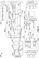
FIG. 1 depicts an apparatus that may employ a communication link between integrated circuit (IC) devices. In one example, theapparatus 100 may include a wireless communication device that communicates through an RF transceiver with a radio access network (RAN), a core access network, the Internet and/or another network. Theapparatus 100 may include acommunications transceiver 106 operably coupled toprocessing circuit 102. Theprocessing circuit 102 may include one or more IC devices, such as an application-specific IC (ASIC) 108. TheASIC 108 may include one or more processing devices, logic circuits, and so on. Theprocessing circuit 102 may include and/or be coupled to processor readable storage such as amemory 112 that can maintain data and instructions that may be executed by processingcircuit 102. Theprocessing circuit 102 may be controlled by one or more of an operating system and an application programming interface (API) 110 layer that supports and enables execution of software modules residing in storage media, such as thememory device 112 of the wireless device. Thememory device 112 may include read-only memory (ROM) or random-access memory (RAM), electrically erasable programmable ROM (EEPROM), flash cards, or any memory device that can be used in processing systems and computing platforms. Theprocessing circuit 102 may include or access alocal database 114 that can maintain operational parameters and other information used to configure and operate theapparatus 100. Thelocal database 114 may be implemented using one or more of a database module, flash memory, magnetic media, EEPROM, optical media, tape, soft or hard disk, or the like. The processing circuit may also be operably coupled to external devices such as anantenna 122, adisplay 124, operator controls, such asbutton 128 andkeypad 126 among other components. - One or more of the components illustrated in
FIG. 1 may implement clock and data recovery, according to one or more aspects described herein, to recover a clock embedded within differential signal transitions in a multi-wire (N-Wire) communication system (e.g., N-factorial N! encoding, and N-phase encoding). Note that the terms "wires", "conductors, "connectors", and/or "lines" may be interchangeably used to refer to the electrical paths through which differential signals may be transmitted. -
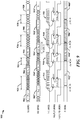
FIG. 2 is a block schematic 200 illustrating certain aspects of anapparatus 200 such as a mobile apparatus that employs acommunication link 220 to connect various subcomponents. In one example, theapparatus 200 includes a plurality ofIC devices communication link 220. Thecommunication link 220 may be used to connectIC devices apparatus 200. In one example, thecommunication link 220 may be provided on a chip carrier, substrate or circuit board that carries theIC devices first IC device 202 may be located in a keypad section of a flip-phone while asecond IC device 230 may be located in a display section of the flip-phone. In another example, a portion of thecommunication link 220 may include a cable or optical connection. - The
communication link 220 may providemultiple channels more channels 226 may be bidirectional, and may operate in half-duplex and/or full-duplex modes. One ormore channels communication link 220 may be asymmetrical, providing higher bandwidth in one direction. In one example described herein, afirst communications channel 222 may be referred to as aforward link 222 while asecond communications channel 224 may be referred to as areverse link 224. Thefirst IC device 202 may be designated as a host system or transmitter, while thesecond IC device 230 may be designated as a client system or receiver, even if bothIC devices forward link 222 may operate at a higher data rate when communicating data from afirst IC device 202 to asecond IC device 230, while thereverse link 224 may operate at a lower data rate when communicating data from thesecond IC device 230 to thefirst IC device 202. - The
IC devices device first IC device 202 may perform core functions of theapparatus 200, including maintaining wireless communications through awireless transceiver 204 and anantenna 214, while thesecond IC device 230 may support a user interface that manages or operates adisplay controller 232. In the example, thesecond IC device 230 may be adapted to control operations of a camera or video input device using acamera controller 234. Other features supported by one or more of theIC devices display controller 232 may include circuits and software drivers that support displays such as a liquid crystal display (LCD) panel, touch-screen display, indicators and so on. Thestorage media respective processors IC devices processor corresponding storage media more bus - The
reverse link 224 may be operated in the same manner as theforward link 222, and theforward link 222 andreverse link 224 may be capable of transmitting at comparable speeds or at different speeds, where speed may be expressed as data transfer rate and/or clocking rates. The forward and reverse data rates may be substantially the same or differ by orders of magnitude, depending on the application. In some applications, a singlebidirectional link 226 may support communications between thefirst IC device 202 and thesecond IC device 230. Theforward link 222 and/orreverse link 224 may be configurable to operate in a bidirectional mode when, for example, the forward and reverselinks communication link 220 may be operated to communicate control, command and other information between thefirst IC device 202 and thesecond IC device 230 in accordance with an industry or other standard. - In one example, forward and reverse
links links devices 210 and/or 230 can encode multiple bits per clock transition, and multiple sets of wires can be used to transmit and receive data from the SDRAM, control signals, address signals, and so on. - The forward and reverse
links processor IC device 202 and anIC device 230 that supports the camera or display in a mobile device. The MIPI standard includes specifications that govern the operational characteristics of products that comply with MIPI specifications for mobile devices. The MIPI standard may define interfaces that employ complimentary metal-oxide-semiconductor (CMOS) parallel busses. - The
communication link 220 ofFIG. 2 may be implemented as a wired bus that includes a plurality of signal wires (denoted as N wires). The N wires may be configured to carry data encoded in symbols, where clock information is embedded in a sequence of the symbols transmitted over the plurality of wires. Examples of encoding techniques used with N-wire interfaces include N-factorial (N!) encoding, and N-phase encoding. - The
IC devices 202 and/or 230 (and/or components therein) illustrated inFIG. 2 may implement clock and data recovery, according to one or more aspects described herein, to recover a clock embedded within differential signal transitions in a multi-wire (N-Wire) communication system (e.g., N-factorial N! encoding, and N-phase encoding). -
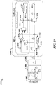
FIG. 3 illustrates a general 3-wire differential signaling scheme between atransmitter device 300 and areceiver device 301 based states defined by differential signals among a plurality of conductors/wires A, B, and C. The combinations of differential values (e.g., from 3 or more conductors) in a particular cycle may define a state or symbol. Thetransmitter device 300 andreceiver device 301 may communicate over amulti-line bus 308. In this example, three lines A, B, and C are used for thebus 308. Thereceiver device 301 may include a three-port receiver 310 to couple thereceiver device 301 to thebus 308. - A clock signal is embedded within this 3-wire differential signaling by guaranteeing that there is a symbol change every cycle. A clock data recovery circuit that extracts a clock signal from the differential signal must also minimize jitter. This clock signal may be used to synchronize decoding of the symbols in the 3-wire differential signal. While certain logic circuits may serve to minimize jitter, these require a relatively large number of logic devices, which is a problem when scaling up to n-wire differential signaling.
- In one example, differential signal encoding may be used to transmit signals from the
transmitter device 300 thereceiver device 301. Consequently, each of a plurality of receivers 312 may be configured to take two of the three lines A, B, and C and provide a different signal. For instance, a first line A and a second line B may serve to provide a firstdifferential signal RX_AB 314, the second line B and a third line C may serve to provide a seconddifferential signal RX_BC 316, and the first line A and the third line C may serve to provide a thirddifferential signal RX_CA 318. Thesedifferential signals decoder circuit 320. Thedecoder circuit 320 decodes the three differentialsignals RX AB 314,RX_BC 316, andRX_CA 318 and outputs the six states XM, YM, ZM, ZP, YP, and XP. In one example, each of the six states XM, YM, ZM, ZP, YP, and XP may represent a symbol, and the encoding used guarantees a symbol-to-symbol state transition for transmitted signals. The combination ofdifferential signals RX_AB 314,RX_BC 316, andRX_CA 318 may be referred to a spread signal, where the spread signal carries the symbols. Due to their guaranteed state transitions, each of the differential signalsRX_AB 314,RX_BC 316, andRX_CA 318 may be referred to as a state transition signal. - In this example, the receivers 312 are illustrated as differential receivers which take as inputs two signals from two different wires (e.g., AB, BC, AC) and output a differential signal (i.e., the output signal being the difference between the two input signals). In one example, the voltage difference between two wires/conductors may define a differential signal. In another example, the current flow direction in each wire/conductor may also be used (alone or in combination with voltage) define a differential signal.
- A state diagram 303 illustrates the six (6) states XM, YM, ZM, ZP, YP, and XP that may be defined by the
differential signals C 308. As can be observed, the voltage levels across the threedifferential signals - In addition to the information encoded in the states (e.g., 3 bits per state), information may also be encoded based on transitions between the states. Note that transition between any two states (XM, YM, ZM, ZP, YP, and XP) occurs in a single step without traversing intermediate states. As such, differential data transmission schemes based on the state diagram 303 would be free of state transition decoding problems.
- Each of the conductors of the
bus 308 may be driven High, driven Low, or undriven, with only one conductor being undriven in any single cycle. In one embodiment, three differential signals,RX_AB 314,RX_BC 316, and RX_CA 318 (e.g., received by adecoder 320 within receiver device 301), are defined as positive differential voltage tologic 1 and negative differential voltage tologic 0 between conductor A relative to conductor B, conductor B relative to conductor C, and conductor C relative to conductor A respectively. Example waveforms of the threedifferential signals - Six possible states (excluding the states that cause a zero differential voltage between conductor A relative to conductor B, conductor B relative to conductor C, and conductor C relative to conductor A) are defined as XM, YM, ZP, ZM, YP, XP, and XM by states of the
signals RX_AB 314,RX_BC 316, andRX_CA 318 according to state diagram 303. - State signals corresponding to the six possible states XM, YM, ZP, ZM, YP, XP, and XM are generated from the differential signals
RX_AB 314,RX BC 316, andRX CA 318 by a decoder block 320 (DEC), in thereceiver device 301, and exemplary waveforms of the state signals are shown in the diagram 305. - In one embodiment, a state transition from a state, XM, YM, ZP, ZM, YP, XP, or XM, to a different state always occurs at any single cycle in a way that a state transition represents data to be transmitted from the
transmitter device 300 to thereceiver device 301. - In an alternative embodiment, single-ended signaling may be used over the conductors/wires A, B, C of the
multi-line bus 308. In one example of single-ended signaling, one conductor/wire may carry a varying voltage that represents the signal while another conductor/wire may be connected to a reference voltage (e.g., ground). In the case of such single-ended signaling, thetransmitter device 300 may include a plurality of single-ended open-drain (transistor) drivers, each driver coupled to a single wire/conductor A, B, C of themulti-line bus 308. Thereceiver device 301 may include one or more single-ended receivers (e.g., complementary metal-oxide-semiconductor (CMOS) transistors), where each single-ended receiver is coupled to a single wire/conductor A, B, C of themulti-line bus 308. Thetransmitter device 300 may receive input bits, encodes them into single-ended signals, and transmits the single-ended signals to thereceiver device 301 through single-ended drivers via each wire/conductor A, B, C of themulti-line bus 308. Thereceiver device 301 receives the single-ended signals via each wire/conductor A, B, C of themulti-line bus 308 through the single-ended receivers, decodes the single-ended signals, and provides output bits. In this single-ended system, thedecoder 320 may include a clock and data recovery (CDR) such that a clock signal is extracted from one or more received single-ended signals. -
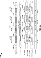
FIG. 4 is a diagram illustrating an example of N-factorial (N!) encoding used on an N-wire interface 400 provided between twodevices transmitter 402, atranscoder 406 may be used to encodedata 404 and clock information in symbols to be transmitted over a set of N wires 414. The clock information may be derived from a transmitclock 412 and may be encoded in a sequence of symbols transmitted in N C2 differential signals over the N wires 414 by ensuring that a signaling state transition occurs on at least one of the N C2 signals between consecutive symbols. When N! encoding is used to drive the N wires 414, each bit of a symbol is transmitted as a differential signal by one of a set ofdifferential line drivers 410, where the differential drivers in the set ofline drivers 410 are coupled to different pairs of the N wires. The number of available combinations of wire pairs ( N C2) determines the number of signals that can be transmitted over the N wires 414. The number ofdata bits 404 that can be encoded in a symbol may be calculated based on the number of available signaling states available for each symbol transmission interval. - A termination impedance (typically resistive) couples each of the N wires 414 to a
common center point 418 in atermination network 416. It will be appreciated that the signaling state of the N wires 414 reflects a combination of the currents in thetermination network 416 attributed to thedifferential drivers 410 coupled to each wire. It will be further appreciated that thecenter point 418 is a null point, whereby the currents in thetermination network 416 cancel each other at the center point. - The N! encoding scheme need not use a separate clock channel and/or non-return-to-zero decoding because at least one of the N C2 signals in the link transitions between consecutive symbols. Effectively, each
transcoder 406 ensures that a transition occurs between each pair of symbols transmitted on the N wires 414 by producing a sequence of symbols in which each symbol is different from its immediate predecessor symbol. In the example depicted inFIG. 4 , four wires are provided (N=4), and the 4 wires can carry 4C2 = 6 differential signals. Thetranscoder 406 may employ a mapping scheme to generate raw symbols for transmission on the N wires 414. Thetranscoder 406 may mapdata bits 404 to a set of transition numbers. The transition numbers may be used to select raw symbols for transmission based on the value of the immediately preceding symbol such that the selected raw symbol is different from the preceding raw symbol. The raw symbols may be serialized by theserializer 408 to obtain a sequence of symbols for transmission over the N-wires 414. In one example, a transition number may be used to lookup a data value corresponding to the second of the consecutive raw symbols with reference to the first of the consecutive raw symbols. At thereceiver 420, atranscoder 428 may employ a mapping to determine a transition number that characterizes a difference between a pair of consecutive raw symbols in a lookup table, for example. Thetranscoders - The
transcoder 406 at thetransmitter 402 may select between N! - 1 available signaling states at every symbol transition. In one example, a 4! system provides 4! - 1 = 23 signaling states for the next symbol to be transmitted at each symbol transition. The bit rate may be calculated as log2(available_states) per transmit clock cycle. - According to certain aspects disclosed herein, dual data rate (DDR) signaling may be employed to increase the interface bandwidth by transmitting two symbols in each period of the transmit
clock 412. Symbol transitions occur at both the rising edge and falling edge of the transmit clock in a system using double data rate (DDR) clocking. The total available states in the transmit clock cycle is (N! - 1)2 = (23)2 = 529 and the number ofdata bits 404 that can transmitted over two symbol may be calculated as log2 (529) = 9.047 bits. - A receiving
device 420 receives the sequence of symbols using a set ofline receivers 422 where each receiver in the set ofline receivers 422 determines differences in signaling states on one pair of the N wires 414. Accordingly, N C2 receivers are used, where N represents the number of wires. The N C2 receivers 422 produce a corresponding number of raw symbols as outputs. In the depicted 4-wire example, the signals received on the 4 wires 414 are processed by 6 receivers (4C2 = 6) to produce araw symbol signal 432 that is provided to aCDR 424 anddeserializer 426. Theraw symbol signal 432 is representative of the signaling state of the N wires 414, and theCDR 424 may process theraw symbol signal 432 to generate a receiveclock signal 434 that can be used by thedeserializer 426. - The receive
clock signal 434 may be a DDR clock signal that can be used by external circuitry to process receiveddata 430 provided by thetranscoder 428. Thetranscoder 428 decodes a block of received symbols from thedeserializer 426 by comparing each symbol to its immediate predecessor. Thetranscoder 428 producesoutput data 430 corresponding to thedata 404, provided to thetransmitter 402. - Certain other multi-wire interfaces use N-phase encoding to transmit data over a plurality of wires.
- It should be noted that the system illustrated in
FIG. 4 may also be implemented using single-ended signaling and single-ended drivers/receivers between thetransmitter device 402 and thereceiver device 420 in place of differential signaling anddifferential drivers 410 anddifferential receivers 422. When single-ended signaling and single-ended drivers/receivers are used between thetransmitter device 402 and thereceiver device 420, thetermination network 416 illustrated inFIG. 4 can be excluded. -
FIG. 5 is a diagram 500 illustrating an example of an M-wire, N-phase polarity encoding transmitter configured for M=3 and N=3. The principles and techniques disclosed for 3-wire, 3-phase encoders can be applied in other configurations of M-wire, N-phase polarity encoders. - When N-phase polarity encoding is used, conductors such as
signal wires undriven signal wire undriven signal wire undriven signal wire FIG. 6 , a set of drivers 508 (FIG. 5 ) may control the state of eachsignal wire signal wire drivers 508 may include unit-level current-mode drivers. In another example,drivers 508 may drive opposite polarity voltages on twosignals third signal 510c is at high impedance and/or pulled to ground. For each symbol transmission interval, at least one signal is in the undriven (0) state, while the number of signals driven positive (+1 state) is equal to the number of signals driven negative (-1 state), such that the sum of current flowing to the receiver is always zero. For each pair of consecutive symbol transmission intervals, at least onesignal wire - In the example depicted in
FIG. 5 , 16-bit data 418 is input to amapper 502, which maps theinput data 518 to 7symbols 512 for transmitting sequentially over thesignal wires symbols 512 may be serialized, using parallel-to-serial converters 504 for example. A 3-wire, 3-phase encoder 406 receives 7symbols 512 produced by the mapper one symbol at a time and computes the state of eachsignal wire encoder 506 selects the states of thesignal wires signal wires - The use of M-wire, N-phase encoding permits a number of bits to be encoded in a plurality of symbols where the bits per symbol is not an integer. In the simple example of a 3-wire system, there are 3 available combinations of 2 wires that may be driven simultaneously, and 2 possible combinations of polarity on the pair of simultaneously driven wires, yielding 6 possible states. Since each transition occurs from a current state, 5 of the 6 states are available at every transition. The state of at least one wire is required to change at each transition. With 5 states, log2(5) ≅ 2.32 bits may be encoded per symbol. Accordingly, a mapper may accept a 16-bit word and convert it to 7 symbols because 7 symbols carrying 2.32 bits per symbol can encode 16.24 bits. In other words, a combination of seven symbols that encodes five states has 57 (78,125) permutations. Accordingly, the 7 symbols may be used to encode the 216 (65,536) permutations of 16 bits.
-
FIG. 6 illustrates an example of signaling 600 employing a three-phase modulation data-encoding scheme based on the circular state transition diagram 650. According to the data-encoding scheme, a three-phase signal may rotate in two directions and may be transmitted on threeconductors conductors conductor conductors conductors conductors conductors - At any phase state in the illustrated three-wire example, exactly two of the
conductors third conductor conductor conductor other conductor conductor - In the example of a three-wire, three-phase communications link, clockwise rotations (S1 to S2), (S2 to S3), and/or (S3 to S1) at a state transition may be used to encode a
logic 1, while counter-clockwise rotations (S1 to S3), (S3 to S2), and/or (S2 to S1) at the state transition may be used to encode alogic 0. Accordingly a bit may be encoded at each transition by controlling whether the signal is "rotating" clockwise or counter-clockwise. For example, alogic 1 may be encoded when the threewires logic 0 may be encoded when the threewires wires - Information may also be encoded in the polarity of the driven
conductors conductors Signals conductors first conductor second conductor third conductor second conductors second conductors active conductors active conductors - In the example of the three-wire, three-phase link described herein, one bit of data may be encoded in the rotation, or phase change in the three-wire, three-phase link, and an additional bit may be encoded in the polarity of two driven wires. Certain embodiments, encode more than two bits in each transition of a three-wire, three-phase encoding system by allowing transition to any of the possible states from a current state. Given three rotational phases and two polarities for each phase, 6 states are defined, such that 5 states are available from any current state. Accordingly, there may be log2(5) ≅ 2.32 bits per symbol (transition) and the mapper may accept a 16-bit word and convert it to 7 symbols.
-
FIG. 7 is a blockschematic drawing 700 illustrating an exemplary receiver in a 3-phase interface. A plurality ofcomparators 702 and adecoder 704 are configured to provide a digital representation of the state of each of three transmission lines orconductor conductor conductor conductor decoder 704 based on the outputs of thecomparators 702. Seven consecutive states are assembled by serial to parallel converters ordeserializers 706, which produce sets of 7 symbols to be processed by ademapper 708 to obtain 16 bits of data that may be buffered in a first in first out buffer (FIFO) 710. Thedecoder 704 may include aCDR circuit 714 configured to extract a receiveclock 716 from transitions in signaling states between consecutive pairs of transmitted symbols.Table 1. Wire amplitude Diff. Rx output Receiver Digital Output State A B C A-B B-C C-A Rx_AB Rx_BC Rx_CA +x + V 0 +V/2 +V -V/2 -V/2 1 0 0 -x 0 +V +V/2 -V +V/2 +V/2 0 1 1 +y +V/2 +V 0 -V/2 +V -V/2 0 1 0 -y +V/2 0 +V +V/2 -V +V/2 1 0 1 + z 0 +V/2 +V -V/2 -V/2 + V 0 0 1 -Z +V +V/2 0 +V/2 +V/2 - V 1 1 0 - Table 1 illustrates the operation of the
differential receivers 702. In this example, the wire states may be encoded in the voltage amplitude on the threewires differential receivers 702 for each wire in the 3-wire 3-Phase Polarity encoding system. A receiver/decoder may be configured to output a code at the digital output of the receiver for each symbol decoded. - Certain N-wire interfaces may be adapted to provide increased bandwidth through the use of DDR clocking, whereby a new symbol is transmitted at both the rising and falling edges of a transmit clock. However, conventional CDR circuits may be unable to respond to DDR clocking and/or conventional CDR circuits may limit the maximum possible operation speed of an N! wire or N-phase interface.
-
FIG. 8 is a schematic diagram 800 including anexemplary CDR circuit 808 that illustrates certain aspects of clock and data recovery from a multi-wire interface. -
FIG. 9 illustrates an example of timing of certain signals generated by theCDR circuit 808. TheCDR circuit 808 may be used with a variety of multi-wire interfaces, including interfaces that use N! encoding, N-phase encoding, and other encoding schemes that use symbol transition clocking, including interfaces that employ single-ended multi-wire communication links. - A
receiver circuit 800 may include a four-wire termination network 804, a plurality of receivers (Rcvrs) 806, and a clock anddata recovery circuit 808. In one example, a clock is embedded in symbol transitions within a spread signal distributed across four wires orconductors 802. TheCDR circuit 808 may be configured to extract a clock and data symbols from the spread signal received over the four wires orconductors 802. The spread signal may be defined by a plurality of transition signals including a first signal over a first line interface, conductor, or wire. TheCDR circuit 808 may include acomparator 810, a set-reset latch 814, a first analogdelay device S 818, and a second analogdelay device T 822. Aclock extraction circuit 809 may be defined by thecomparator 810, a set-reset latch 814, and a first analogdelay device S 818. Theclock extraction circuit 809 may be adapted to extract a signal that may be used to obtain a clock signal from state transition in the received first signal. Since the spread signal carries symbols with guaranteed symbol-to-symbol state transitions between consecutive symbols, these transitions are detected and used to generate the clock signal. The clock signal may be obtained using jitter compensation and serves to sample symbols from the spread signal distributed over the plurality ofreceivers 806. - The
comparator 810 may compare a first instance of the first signal (SI) 830 and a delayed second instance of the first signal (SD) 832 (i.e., delayed by the second analog delay device T 822), and thecomparator 810 outputs a comparison signal (NE signal) 812. The set-reset latch 814 may receive the NE signal 812 from thecomparator 810 and provides a filtered version of the comparison signal (NEFLT signal) 816. The first analogdelay device S 818 receives theNEFLT signal 816 and outputs a delayed instance of theNEFLT signal 816 as theNEFLTD signal 820. TheNEFLTD signal 820 serves as the reset input to the set-reset latch 814 such that the output of the set-reset latch 814 is reset after a delay S. In one example, theNEFLT signal 816 may be used as the clock signal to sample symbols. - The second
analog delay device 822 may receive the first instance of the first signal (SI) 830 and provides a delayed second instance of the first signal (SD) 832 to thecomparator 810. In one example, the spread signal distributed across the plurality of wires orconductors 802 and may include or is defined a plurality of distinct state transition signals which, when combined, carry symbols with guaranteed symbol-to-symbol state transitions between consecutive symbols. For example, for the case of three conductors using differential signaling inFIG. 3 , spread signal may be defined by the combination of the differential signalsRX_AB 314,RX_BC 316, orRX_CA 318. The first signal may be one of the differential signalsRX_AB 314,RX_BC 316, orRX_CA 318. The first instance of the first signal (SI) 830 may comprise, for example, all or a portion/segment of any one of the differential signalsRX_AB 314,RX_BC 316, orRX_CA 318. - A flip-
flop device 826 may also receive the delayed second instance of the first signal (SD) 832 and outputs a symbol (S) 834 triggered by theNEFLT signal 816. That is, the flip-flop device 826 is triggered by a rising edge on theNEFLT signal 816. Consequently, the secondanalog delay device 822 serves to generate the NE signal 812. In turn, the NE signal 812 serves to generate theNEFLT signal 816 which serves as a latching clock for the flip-flop device 826. - In operation, when a transition occurs between a current symbol (S0) 904 and a next symbol (S1) 906, the state of the
SI signal 830 begins to change. The NE signal 812 transitions high when thecomparator 810 first detects a difference between theSI signal 830 and theSD signal 832, causing the set-reset latch 814 to be asynchronously set. Accordingly, the NEFLT signal 816 transitions high, and this high state is maintained until the set-reset latch 814 is reset when theNEFLTD signal 820 becomes high. The NEFLT signal 816 transitions to a high state in response to the rising edge of the NE signal 812, and the NEFLT signal 816 transitions to a low state in response to the rising edge of theNEFLTD signal 820 after a delay attributable to the first analogdelay device S 818. - As transitions between
symbols indeterminate states SI 830 may be regarded as invalid data, and these intermediate states may causespikes comparator 810 returns towards a low state for short periods of time. Thespikes NEFLT signal 816 output by the set-reset latch 814. The set-reset latch 814 effectively blocks and/or filters out thespikes NEFLT signal 816. - The flip-
flop device 826 may have a negative hold time (-ht) as theinput symbols flop device 826. For instance, each symbol 902', 904', 906' and 908' in theSD signal 832 is set or captured by the flip-flop device 826 at the rising clock edge of theNEFLT signal 816, which occurs after theinput symbols SI signal 830. - Various elements illustrated in the
CDR circuit 808 may be implemented by various subcircuits. For example, the set-reset latch 814 may be implemented as a first logic circuit 814', the analogdelay S device 818 may be implemented as a series of inverters 818', and thecomparator 810 may be implemented as a second logic circuit 810'. - The first logic circuit 814' may include an
inverter 840, an ORgate 842, afirst NAND gate 844, and asecond NAND gate 846. - The second logic circuit 810' may include a plurality of
XNOR gates 848 whose outputs all serve as inputs to aNAND gate 850. The output of theNAND gate 850 may serve as the NE signal 812. Each input signal SI[x] into each of theXNOR gates 848 may correspond to a distinct state transition signal carrying part of the spread signal. For example, in the case of differential signaling ofFIG. 3 , the first signal SI[0] may be the firstdifferential signal RX_AB 314, a second signal SI[1] may be the seconddifferential signal RX_BC 316, and a third signal SI[2] may be the thirddifferential signal RX_CA 318. - While the
CDR circuit 808 is tolerant to jitter, it is achieved using only nC2 analog delays and 2xnC2 input comparators without the need for 2xnC2 flip-flops, where nC2 is the number of available combinations of wire pairs ( n ). For example, inU.S. Patent No. 8064535 ,FIG. 13 illustrates a clock and data recovery circuit using 2xnC2 flip-flops (i.e., twelve flip-flops for a combination of six wire pairs) and nC2 + 1 analog delays (i.e., seven analog delays for a combination of six wire pairs). Both flip-flops and analog delays are expensive resources to include in a CDR circuit, so minimizing their use is desirable. By comparison, inFIG. 8 theCDR circuit 808 may be implemented using nC2 + 1analog delays 818 and 822 (i.e., seven analog delays for a combination of six wire pairs) and nC2 XNOR gates 848 (i.e., six comparator gates for a combination of six wire pairs). -
FIG. 10 is a block diagram 1000 including anexemplary CDR circuit 1008 that illustrates certain aspects of clock and data recovery from a multi-wire interface. -
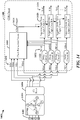
FIG. 11 is a timing diagram 1100 illustrating the operation of theCDR circuit 1008 under typical operating conditions. TheCDR circuit 1008 may be used with a variety of multi-wire interfaces, including interfaces that use N! encoding, N-phase encoding, and other encoding schemes that use symbol transition clocking, including interfaces that employ single-ended multi-wire communication links. - A
receiver circuit 1000 may include a four-wire termination network 1004, a plurality ofreceivers 1006, and a clockdata recovery circuit 1008. In one example, a clock is embedded in symbol transitions within a spread signal distributed across four wires orconductors 1002. - The
CDR circuit 1008 may be configured to extract a clock and data symbols from the spread signal received over the four wires orconductors 1002. The spread signal may be defined by a plurality of transition signals including a first signal over a first line interface, conductor, or wire. TheCDR circuit 1008 may include acomparator 1010, a set-reset latch 1014, a first analogdelay device S 1018, a second analogdelay device T 1022, and alevel latch 1028. Aclock extraction circuit 1009 may be defined by thecomparator 1010, a set-reset latch 1014, and a first analogdelay device S 1018. Theclock extraction circuit 1009 may be adapted to extract a signal that may be used to obtain a clock signal from state transitions within the received first signal. Since the received spread signal carries symbols with guaranteed symbol-to-symbol state transitions between consecutive symbols, these transitions are detected and used to generate the clock signal. The clock signal may be obtained using jitter compensation and serves to sample symbols from the spread signal distributed over the plurality ofreceivers 1006. - The
comparator 1010 may compare a first instance of the first signal (SI) 1030 and a delayed second instance of the first signal (SD) 1032, and thecomparator 1010 outputs a comparison signal (NE signal) 1012. The set-reset latch 1014 may receive theNE signal 1012 from thecomparator 1010 and provides a filtered version of the comparison signal (NEFLT signal) 1016. The first analogdelay device S 1018 receives theNEFLT signal 1016 and outputs a delayed instance of theNEFLT signal 1016 as theNEFLTD signal 1020. TheNEFLTD signal 1020 serves as the reset input to the set-reset latch 1014 such that the output of the set-reset latch 1014 is reset after a delay S. In one example, theNEFLT signal 1016 may be used as the clock signal to sample symbols. - Various elements illustrated in the
CDR circuit 1008 may be implemented by various subcircuits. For example, the set-reset latch 1014 may be implemented as a first logic circuit 814' (FIG. 8 ), the analogdelay S device 1018 may be implemented as a series of inverters 818', and thecomparator 1010 may be implemented as a second logic circuit 810' (FIG. 8 ). - In one example, the spread signal distributed across the wires or
conductors 1002 may include a plurality of distinct transition signals which, when combined, carry symbols with guaranteed symbol-to-symbol state transitions between consecutive symbols. For example, for the case of three conductors using differential signaling inFIG. 3 , spread signal may be defined by the combination of the differential signalsRX_AB 314,RX_BC 316, orRX_CA 318. The first signal may be one of the differential signalsRX_AB 314,RX_BC 316, orRX_CA 318. The first instance of the first signal (SI) 830 may comprise, for example, all or a portion/segment of any one of the differential signalsRX_AB 314,RX_BC 316, orRX_CA 318. - A
level latch 1028 receives the first instance of the first signal (SI) 1030 and provides the delayed second instance of the first signal (SD) 1032 to thecomparator 1010. Thelevel latch 1028 is triggered by a delayed instance of theNE signal 1012. A flip-flop device 1026 may also receive the delayed second instance of the first signal (SD) 1032 and outputs a symbol (S) 1034 triggered by theNEFLT signal 1016. That is, the flip-flop device 1026 is triggered by a rising edge on theNEFLT signal 1016. Consequently, thelevel latch 1028 and secondanalog delay device 1022 serve to generate theNE signal 1012. In turn, theNE signal 1012 serves to generate theNEFLT signal 1016 which serves as a latching clock for the flip-flop device 1026. - In operation, when a transition occurs between a current symbol (S0) 1104 and a next symbol (S1) 1106, the state of the
SI signal 1030 begins to change. The NE signal 1012 transitions high when thecomparator 1010 first detects a difference between theSI signal 1030 and theSD signal 1032, causing the set-reset latch 1014 to be asynchronously set. Accordingly, theNEFLT signal 1016 transitions high, and this high state is maintained until the set-reset latch 1014 is reset when theNEFLTD signal 1020 becomes high. TheNEFLT signal 1016 transitions to a high state in response to the rising edge of theNE signal 1012, and theNEFLT signal 1016 transitions to a low state in response to the rising edge of theNEFLTD signal 1020 after a delay attributable to the first analogdelay device S 1018. - As transitions between
symbols indeterminate states SI signal 1030 due to inter-wire skew, signal overshoot, signal undershoot, crosstalk, and so on. The intermediate states on theSI signal 1030 may be regarded as invalid data, and these intermediate states may causespikes NE signal 1012 as the output of thecomparator 1010 returns towards a low state for short periods of time. Thespikes NEFLT signal 1016 output by the set-reset latch 1014. The set-reset latch 1014 effectively blocks and/or filters out thespikes NE signal 1012 from theNEFLT signal 1016. - The flip-
flop device 1026 may have a negative hold time (-ht) as theinput symbols SI signal 1030 can change prior to the symbol being latched or captured by the flip-flop device 1026. For instance, each symbol 1102', 1104', 1106' and 1108' in theSD signal 1032 is set or captured by the flip-flop device 1026 at the rising clock edge of theNEFLT signal 1016, which occurs after theinput symbols SI signal 1030. - In comparison to the
first CDR circuit 808 inFIG. 8 , thesecond CDR circuit 1008 inFIG. 10 provides a wider and/or more stable symbols within theSD signal 1032. In particular, by triggering thelevel latch 1028 using a delayed version of the NE signal (signal NED 1024), a stable version of the delayed second instance of the first signal (SD signal 1032) can be latched in more quickly, resulting in a stable wider symbol. For example, inFIG. 9 , a symbol S1 906' may have a width A in the SD signal 832 while inFIG. 11 the corresponding symbol S1 1106' may have a width B in theSD signal 1032, where width B > width A. Since the stable symbol portion of theSD signal 1032 is wider in this approach, this provides a wider sampling margin so a faster transmission link may be possible relative to the approach inFIGS. 8 and9 . - Relative to the CDR circuit in
FIG. 13 ofU.S. Patent No. 8064535 , which uses 2x nC2 flip-flops and nC2 + 1 analog delays, theCDR circuit 1008 ofFIG. 10 is implemented using only twoanalog delays -
FIG. 12 is a block diagram 1200 including anexemplary CDR circuit 1208 that illustrates certain aspects of clock and data recovery from a multi-wire interface. -
FIG. 13 is a timing diagram 1300 illustrating the operation of theCDR circuit 1208 under typical operating conditions. TheCDR circuit 1208 may be used with a variety of multi-wire interfaces, including interfaces that use N! encoding, N-phase encoding, and other encoding schemes that use symbol transition clocking, including interfaces that employ single-ended multi-wire communication links. - A
receiver circuit 1200 may include a four-wire termination network 1204, a plurality ofreceivers 1206, and a clockdata recovery circuit 1208. In one example, a clock is embedded in symbol transitions within a spread signal received across four wires orconductors 1202. The spread signal may be defined by a plurality of transition signals including a first signal over a first line interface, conductor, or wire. TheCDR circuit 1208 may be configured to extract a clock and data symbols from the spread signal received over the four wires orconductors 1202. TheCDR circuit 1208 may include acomparator 1210, a set-reset latch 1214, a first analogdelay device S 1218, and alevel latch 1228. Aclock extraction circuit 1209 may be defined by thecomparator 1210, a set-reset latch 1214, and a first analogdelay device S 1218. Theclock extraction circuit 1209 may be adapted to extract a signal that may be used to obtain a clock signal from signals. The clock signal may be obtained using jitter compensation and serves to sample symbols from state transition in the spread signal received over the plurality ofreceivers 1206. - The
comparator 1210 may compare a first instance of the first signal (SI) 1230 and a delayed second instance of the first signal (SD) 1232, and thecomparator 1210 outputs a comparison signal (NE signal) 1212. The set-reset latch 1214 may receive theNE signal 1212 from thecomparator 1210 and provides a filtered version of the comparison signal (NEFLT signal) 1216. The first analogdelay device S 1218 receives theNEFLT signal 1216 and outputs a delayed instance of theNEFLT signal 1216 as theNEFLTD signal 1220. TheNEFLTD signal 1220 serves as the reset input to the set-reset latch 1214 such that the output of the set-reset latch 1214 is reset after a delay S. In one example, theNEFLT signal 1216 may be used as the clock signal to sample symbols. - Various elements illustrated in the
CDR circuit 1008 may be implemented by various subcircuits. For example, the set-reset latch 1214 may be implemented as a first logic circuit 814' (FIG. 8 ), the analogdelay S device 1218 may be implemented as a series of inverters 818', and thecomparator 1210 may be implemented as a second logic circuit 810' (FIG. 8 ). - In one example, the spread signal distributed across the wires or
conductors 1202 may include a plurality of distinct transition signals which, when combined, carry symbols with guaranteed symbol-to-symbol state transitions between consecutive symbols. For example, for the case of three conductors using differential signaling inFIG. 3 , spread signal may be defined by the combination of the differential signalsRX_AB 314,RX_BC 316, orRX_CA 318. The first signal may be one of the differential signalsRX_AB 314,RX_BC 316, orRX_CA 318. The first instance of the first signal (SI) 830 may comprise, for example, all or a portion/segment of any one of the differential signalsRX_AB 314,RX_BC 316, orRX_CA 318. - A
level latch 1228 receives the first instance of the first signal (SI) 1230 and provides the delayed second instance of the first signal (SD) 1232. Thelevel latch 1228 is triggered by the resultingoutput NEFLT_COMP 1236 of anOR gate 1222 which has theNEFLT 1216 andNEFLTD signal 1220 as inputs. - A
level latch 1228 receives the first instance of the first signal (SI) 1230 and provides the delayed second instance of the first signal (SD) 1232 to thecomparator 1210. Thelevel latch 1228 is triggered by a delayed instance of theNE signal 1212. A flip-flop device 1226 may also receive the delayed second instance of the first signal (SD) 1232 and outputs a symbol (S) 1234 triggered by theNEFLT signal 1216. That is, the flip-flop device 1226 is triggered by a rising edge on theNEFLT signal 1216. Consequently, thelevel latch 1228 serves to generate theNE signal 1212. In turn, theNE signal 1212 serves to generate theNEFLT signal 1216 which serves as a latching clock for the flip-flop device 1226. - In operation, when a transition occurs between a current symbol (S0) 1304 and a next symbol (S1) 1306, the state of the
SI signal 1230 begins to change. The NE signal 1212 transitions high when thecomparator 1210 first detects a difference between theSI signal 1230 and theSD signal 1232, causing the set-reset latch 1214 to be asynchronously set. Accordingly, theNEFLT signal 1216 transitions high, and this high state is maintained until the set-reset latch 1214 is reset when theNEFLTD signal 1220 becomes high. TheNEFLT signal 1216 transitions to a high state in response to the rising edge of theNE signal 1212, and theNEFLT signal 1216 transitions to a low state in response to the rising edge of theNEFLTD signal 1220 after a delay attributable to the first analogdelay device S 1218. - As transitions between
symbols indeterminate states SI signal 1230 due to inter-wire skew, signal overshoot, signal undershoot, crosstalk, and so on. The intermediate states on theSI signal 1230 may be regarded as invalid data, and these intermediate states may causespikes NE signal 1212 as the output of thecomparator 1210 returns towards a low state for short periods of time. Thespikes NEFLT signal 1216 output by the set-reset latch 1214. The set-reset latch 1214 effectively blocks and/or filters out thespikes NE signal 1212 from theNEFLT signal 1216. - The flip-
flop device 1226 may have a negative hold time (-ht) as theinput symbols SI signal 1230 can change prior to the symbol being latched or captured by the flip-flop device 1226. For instance, each symbol 1302', 1304', 1306' and 1308' in theSD signal 1232 is set or captured by the flip-flop device 1226 at the rising clock edge of theNEFLT signal 1216, which occurs after theinput symbols SI signal 1230. - In comparison to the
first CDR circuit 808 inFIG. 8 and thesecond CDR circuit 1008 inFIG. 10 , thisthird CDR circuit 1208 is implemented without the second analog delay device T while still providing wider or more stable symbols within theSD signal 1232 in relation to the approaches inFIG. 8 andFIG. 10 . TheCDR circuit 1208 ofFIG. 12 is a way to achieve minimum delay while guaranteeing to sample valid data in order to output symbol (S) 1234. Note that theCDR circuit 1008 ofFIG. 10 has no way to make the delay T (i.e., second analog delay device T 1022) as small as the delay (i.e., the delay caused by the OR gate 1222) inFIG. 12 since delay T inFIG. 10 must have a safety margin to account for delay variations due to variations in manufacturing processes, electrical path lengths, temperature, etc. - In particular, by triggering the
level latch 1228 using a delayed version of the NE signal (signal NEFLT_COMP 1236), a stable version of the delayed second instance of the first signal (SD signal 1232) can be latched in more quickly, resulting in a stable wider symbol. For example, inFIG. 9 , a symbol S1 906' may have a width A in the SD signal 832 while inFIG. 13 the corresponding symbol S1 1306' may have a width B in theSD signal 1232, where width B > width A. Since the stable symbol portion of theSD signal 1232 is wider in this approach, this provides a wider sampling margin so a faster transmission link may be possible relative to the approach inFIGS. 8 and9 . - Relative to the CDR circuit in
FIG. 13 ofU.S. Patent No. 8064535 , which uses 2x nC2 flip-flops and nC2 + 1 analog delays, theCDR circuit 1208 ofFIG. 12 is implemented using only oneanalog delay 1218, nC2 level latches 1228, and nC2 XNOR gates 848. Generally, the level latches 1228 are less costly (in terms of resources) to implement than analog delays. -
FIG. 14 is a schematic diagram 1400 including anexemplary CDR circuit 1408 that illustrates certain aspects of clock and data recovery from a multi-wire interface. TheCDR circuit 1408 may be used with a variety of multi-wire interfaces, including interfaces that carry differential signals and/or single-ended signals. In various examples, a N-factorial (N!) encoded signal, a three-phase encoded signal, and/or an N-phase encoded signal by be received over the multi-wire interface. Additionally, other encoding schemes that use symbol transition clocking may also be used to transmit signals over the multi-wire interface. - A
receiver circuit 1400 may include a four-wire termination network 1404, a plurality ofreceivers 1406 and a clock anddata recovery circuit 1408. In one example, thereceivers 1406 may be differential receivers (e.g., whose output is the difference between two input signals). In another example, thereceivers 1406 may be single-ended receivers (e.g., whose output is its input signal relative to a reference, such as ground). When single-ended receivers are used, the termination network 1404 may be excluded. - In one example, a clock is embedded in symbol transitions across four wires or
conductors 1402. TheCDR circuit 1408 may be configured to extract a clock and data symbols from signals received over the four wires orconductors 1402. - A plurality of line interfaces (e.g., defined by the plurality of receivers 1406) may be configured to receive a spread signal distributed over the plurality of line interfaces, the spread signal carrying symbols with guaranteed symbol-to-symbol state transitions between consecutive symbols. The spread signal may be defined by a plurality of transition signals including a first signal over a first line interface. In one example, the first signal may be a differential signal or a single-ended signal. The spread signal may be one of a N-factorial (N!) encoded signal, a three-phase encoded signal, and/or a N-phase encoded signal.
- The
CDR circuit 1408 may include aclock extraction circuit 1410, adelay circuit 1422, and a negative holdtime logic circuit 1426. Theclock extraction circuit 1410 may be adapted to obtain a clock signal from state transitions within the spread signal. The clock signal may be obtained using jitter compensation and serves to sample symbols from the received spread signal distributed over the plurality ofreceivers 1406. For example, the clock signal may be based on a comparison between a first instance of a first signal SI[a] 1430 and a delayed second instance of the first signal SD[a] 1432. Since the spread signal carries symbols with guaranteed symbol-to-symbol state transitions between consecutive symbols, these transitions are detected and used to generate the clock signal. Note that the delayed second instance of the first signal SD[a] 1432 may be obtained by a delay circuit 1422 (e.g.,delay device T 822 inFIG. 8 , the second analogdelay device T 1022 and thelevel latch 1028 inFIG. 10 , and/or theOR gate 1222 and thelevel latch 1228 inFIG. 12 ). - Various examples of the
clock extraction circuit 1410 are found inFIGS. 8 ,10 , and11 , where theNEFLT signal - The
clock extraction circuit 1410 may be adapted to generate a clock signal based on a comparison between a first instance of a first signal SI[a] 1430 and a delayed second instance of the first signal SD[a] 1432. For instance, anNEFLT signal FIGS. 8 ,10 , and12 and may serve as a sampling clock signal for symbol extraction. - In one example, the spread signal is distributed across the wires or
conductors 1002 and may include a plurality of distinct transition signals which, when combined, carry symbols with guaranteed symbol-to-symbol state transitions between consecutive symbols. For example, for the case of three conductors using differential signaling inFIG. 3 , the first signal may be defined by the combination of the differential signalsRX_AB 314,RX_BC 316, andRX_CA 318. The first instance of the first signal (SI) 830 may comprise, for example, any one of the differential signalsRX_AB 314,RX_BC 316, orRX_CA 318. - In one implementation, the
clock extraction circuit 1410 may be further adapted to generate theclock signal 1414 based on additional comparisons between a first instance of a second signal SI[b], within the plurality of state transition signals, and a delayed second instance of the second signal SD[b], and the first signal SI[a] and second signal SI[b] may be concurrent signals received over different line interfaces (plurality of receivers 1406). - A negative hold
time logic circuit 1426 may be adapted to sample the delayed second instance of the first signal SD[a] 1432 based on the clock signal and provide a symbol output S[a] 1434. In one implementation, the negative holdtime logic circuit 1426 includes a separate negative hold time logic device for each of the plurality of line interfaces, each separate negative hold time logic device may be adapted to concurrently sample a delayed instance of a distinct signal SD[a], SD[b], SD[c], ..., SD[n] based on the clock/trigger signal 1414 and provide distinct symbol outputs S[a], S[b], S[c], ..., S[n]. -
FIG. 15 illustrates a method for clock and data recovery. A spread signal may be received distributed over the plurality of line interfaces, the spread signal carrying symbols with guaranteed symbol-to-symbol state transitions between consecutive symbols, the spread signal defined by a plurality of transition signals including a first signal over afirst line interface 1502. In various implementations, the first signal may be a differential signal or a single-ended signal. In some examples, the spread signal may be one of a N-factorial (N!) encoded signal, a three-phase encoded signal, and/or a N-phase encoded signal. - A clock signal may be obtained based on a comparison between a first instance of the first signal and a delayed second instance of the
first signal 1504. The delayed second instance of the first signal may be sampled based on the clock signal to provide asymbol output 1506. The sampling of the delayed second instance of the first signal may be done using a negative hold time logic circuit. - The clock signal may be generated based on additional comparisons between a first instance of a second signal, within the plurality of state transition signals, and a delayed second instance of the second signal, and the first signal and second signal may be concurrent signals received over different line interfaces. A delayed instance of a plurality of distinct received signals may be concurrently sampled based on the clock signal and to provide distinct symbol outputs.
- In one example, obtaining a clock signal may include: (a) comparing the first instance of the first signal (SI) and the delayed instance of the first signal (SD) to provide a comparison signal (NE); (b) latching the comparison signal (NE) to obtain a filtered version of the comparison signal (NEFLT); and/or (c) delaying the filtered version of the comparison signal (NEFLT) to provide a delayed filtered version of the comparison signal (NEFLTD), where the delayed filtered version of the comparison signal (NEFLTD) serves to latch the comparison signal (NE).
- According to a first aspect, illustrated in
FIGS. 8 and9 , the method may further include delaying the first instance of the first signal to obtain the delayed second instance of the first signal. - According to a second aspect, illustrated in
FIGS. 10 and11 , the method may further include: (a) capturing the first instance of the first signal to obtain the delayed second instance of the first signal; and/or (b) delaying the comparison signal (NE) and using the delayed comparison signal (NED) to trigger the latching of the comparison signal (NE). - According to a third aspect, illustrated in
FIGS. 12 and13 , the method may further include capturing the first instance of the first signal to obtain the delayed second instance of the first signal while either the filtered version of the comparison signal (NEFLT) or the delayed filtered version of the comparison signal (NEFLTD) is in a logical high state. - It is understood that the specific order or hierarchy of steps in the processes disclosed is an illustration of exemplary approaches. Based upon design preferences, it is understood that the specific order or hierarchy of steps in the processes may be rearranged. The accompanying method claims present elements of the various steps in a sample order, and are not meant to be limited to the specific order or hierarchy presented.
- While the above discussed aspects, arrangements, and embodiments are discussed with specific details and particularity, one or more of the components, steps, features and/or functions illustrated in
FIGS. 1 ,2 ,3 ,4 ,5 ,6 ,7 ,8 ,9 ,10 ,11 ,12 ,13 ,14 , and/or 15 may be rearranged and/or combined into a single component, step, feature or function or embodied in several components, steps, or functions. Additional elements, components, steps, and/or functions may also be added or not utilized without departing from the present disclosure. The apparatus, devices and/or components illustrated inFIGS. 1 ,2 ,4 ,5 ,7 ,8 ,10 ,12 , and/or 14 may be configured to perform or employ one or more of the methods, features, parameters, and/or steps described inFIGS. 3 ,6 ,9 ,11 ,13 , and/or 15. The novel algorithms described herein may also be efficiently implemented in software and/or embedded in hardware. - Also, it is noted that at least some implementations have been described as a process that is depicted as a flowchart, a flow diagram, a structure diagram, or a block diagram. Although a flowchart may describe the operations as a sequential process, many of the operations can be performed in parallel or concurrently. In addition, the order of the operations may be re-arranged. A process is terminated when its operations are completed. A process may correspond to a method, a function, a procedure, a subroutine, a subprogram, etc. When a process corresponds to a function, its termination corresponds to a return of the function to the calling function or the main function. The various methods described herein may be partially or fully implemented by programming (e.g., instructions and/or data) that may be stored in a non-transitory machine-readable, computer-readable, and/or processor-readable storage medium, and executed by one or more processors, machines and/or devices.
- Those of skill in the art would further appreciate that the various illustrative logical blocks, modules, circuits, and algorithm steps described in connection with the embodiments disclosed herein may be implemented as hardware, software, firmware, middleware, microcode, or any combination thereof. To clearly illustrate this interchangeability, various illustrative components, blocks, modules, circuits, and steps have been described above generally in terms of their functionality. Whether such functionality is implemented as hardware or software depends upon the particular application and design constraints imposed on the overall system.
- The various features associate with the examples described herein and shown in the accompanying drawings can be implemented in different examples and implementations without departing from the scope of the present disclosure. Therefore, although certain specific constructions and arrangements have been described and shown in the accompanying drawings, such embodiments are merely illustrative and not restrictive of the scope of the disclosure, since various other additions and modifications to, and deletions from, the described embodiments will be apparent to one of ordinary skill in the art. Thus, the scope of the disclosure is only determined by the claims which follow.
Claims (15)
- A method operational on a receiver circuit, comprising:receiving a spread signal distributed over a plurality of line interfaces, the spread signal carrying symbols with guaranteed symbol-to-symbol state transitions between consecutive symbols, the spread signal defined by a plurality of state transition signals including a first signal over a first line interface and a second signal over a second line interface;obtaining a clock signal based on a comparison of transitions between a first instance of the first signal and a delayed second instance of the first signal, and a comparison of transitions between a first instance of the second signal and a delayed second instance of the second signal; andsampling the delayed second instance of the first signal based on the clock signal to provide a symbol output.
- The method of claim 1, wherein the first signal is a differential signal.
- The method of claim 1, wherein the first signal is a single-ended signal.
- The method of claim 1, wherein the spread signal is one of a N-factorial (N!) encoded signal, a three-phase encoded signal, or a N-phase encoded signal having three or more phases.
- The method of claim 1, wherein the sampling of the delayed second instance of the first signal is done using a negative hold time logic circuit.
- The method of claim 1, where the first signal and the second signal are concurrent signals received over different line interfaces.
- The method of claim 1, further comprising:
concurrently sampling a delayed instance of a plurality of distinct signals, within the plurality of state transition signals, based on the clock signal to provide distinct symbol outputs. - The method of claim 1, wherein obtaining the clock signal includes:comparing the first instance of the first signal (SI) and the delayed second instance of the first signal (SD) to provide a comparison signal (NE);latching the comparison signal (NE) to obtain a filtered version of the comparison signal (NEFLT); anddelaying the filtered version of the comparison signal (NEFLT) to provide a delayed filtered version of the comparison signal (NEFLTD), wherein the delayed filtered version of the comparison signal (NEFLTD) serves to latch the comparison signal (NE).
- The method of claim 8, further comprising:
delaying the first instance of the first signal to obtain the delayed second instance of the first signal. - The method of claim 8, further comprising:capturing the first instance of the first signal to obtain the delayed second instance of the first signal; anddelaying the comparison signal (NE) and using the delayed comparison signal (NED) to trigger the latching of the comparison signal (NE).
- The method of claim 8, further comprising:
capturing the first instance of the first signal to obtain the delayed second instance of the first signal while either the filtered version of the comparison signal (NEFLT) or the delayed filtered version of the comparison signal (NEFLTD) is in a logical high state. - A receiver circuit (800, 1000, 1200, 1400), comprising:means for receiving (806, 1006, 1206, 1406) a spread signal distributed over a plurality of line interfaces, the spread signal carrying symbols with guaranteed symbol-to-symbol state transitions between consecutive symbols, the spread signal defined by a plurality of state transition signals including a first signal over a first line interface and a second signal over a second line interface;means for obtaining (809, 1009, 1209, 1408) a clock signal based on a comparison of transitions between a first instance of the first signal and a delayed second instance of the first signal, and a comparison of transitions between a first instance of the second signal and a delayed second instance of the second signal; andmeans for sampling (826, 1026, 1226, 1426) the delayed second instance of the first signal based on the clock signal to provide a symbol output.
- The receiver circuit of claim 12, where the first signal and the second signal are concurrent signals received over different line interfaces.
- The receiver circuit of claim 12, further comprising:
means for concurrently sampling a delayed instance of a plurality of distinct signals, within the plurality of state transition signals, based on the clock signal to provide distinct symbol outputs. - The receiver circuit of claim 12, wherein the means for obtaining the clock signal includes:means for comparing the first instance of the first signal (SI) and the delayed second instance of the first signal (SD) to provide a comparison signal (NE);means for latching the comparison signal (NE) to obtain a filtered version of the comparison signal (NEFLT); andmeans for delaying the filtered version of the comparison signal (NEFLT) to provide a delayed filtered version of the comparison signal (NEFLTD), wherein the delayed filtered version of the comparison signal (NEFLTD) serves to latch the comparison signal (NE).
Applications Claiming Priority (5)
| Application Number | Priority Date | Filing Date | Title |
|---|---|---|---|
| US14/199,322 US9363071B2 (en) | 2013-03-07 | 2014-03-06 | Circuit to recover a clock signal from multiple wire data signals that changes state every state cycle and is immune to data inter-lane skew as well as data state transition glitches |
| US14/220,056 US9374216B2 (en) | 2013-03-20 | 2014-03-19 | Multi-wire open-drain link with data symbol transition based clocking |
| US14/252,450 US9178690B2 (en) | 2013-10-03 | 2014-04-14 | N factorial dual data rate clock and data recovery |
| US14/459,132 US9313058B2 (en) | 2013-03-07 | 2014-08-13 | Compact and fast N-factorial single data rate clock and data recovery circuits |
| PCT/US2014/065169 WO2015134071A1 (en) | 2014-03-06 | 2014-11-12 | Clock recovery circuit for multiple wire data signals |
Publications (2)
| Publication Number | Publication Date |
|---|---|
| EP3114792A1 EP3114792A1 (en) | 2017-01-11 |
| EP3114792B1 true EP3114792B1 (en) | 2021-06-09 |
Family
ID=54055706
Family Applications (1)
| Application Number | Title | Priority Date | Filing Date |
|---|---|---|---|
| EP14815119.4A Active EP3114792B1 (en) | 2014-03-06 | 2014-11-12 | Clock recovery circuit for multiple wire data signals |
Country Status (6)
| Country | Link |
|---|---|
| EP (1) | EP3114792B1 (en) |
| JP (1) | JP6219538B2 (en) |
| KR (1) | KR101688377B1 (en) |
| CN (1) | CN106063181B (en) |
| ES (1) | ES2881302T3 (en) |
| WO (1) | WO2015134071A1 (en) |
Families Citing this family (7)
| Publication number | Priority date | Publication date | Assignee | Title |
|---|---|---|---|---|
| BR112018006874A2 (en) * | 2015-10-05 | 2018-10-16 | Qualcomm Inc | multi-track coded n-factor communication systems and other multi-wire communication systems |
| US10628625B2 (en) * | 2016-04-08 | 2020-04-21 | Synopsys, Inc. | Incrementally distributing logical wires onto physical sockets by reducing critical path delay |
| KR102629185B1 (en) * | 2016-12-07 | 2024-01-24 | 에스케이하이닉스 주식회사 | Receiver for data communication |
| FR3102268B1 (en) * | 2019-10-18 | 2023-03-10 | St Microelectronics Rousset | Circuit-on-chip authentication method and associated system-on-chip |
| CN113676992B (en) * | 2020-05-13 | 2022-11-25 | 华为技术有限公司 | Clock signal synchronization method and device |
| KR20220071985A (en) | 2020-11-23 | 2022-06-02 | 한국전자기술연구원 | Dual-mode clock data restoration circuit and method supporting Non-Zero Return and Pulse Amplitude Modulation |
| CN113395414B (en) * | 2021-06-15 | 2022-11-11 | 杭州海康机器人股份有限公司 | Waveform recovery circuit and industrial camera |
Family Cites Families (16)
| Publication number | Priority date | Publication date | Assignee | Title |
|---|---|---|---|---|
| DE3329773A1 (en) * | 1983-08-18 | 1985-02-28 | Siemens AG, 1000 Berlin und 8000 München | Process and arrangement for synchronous edge adaptation of a plurality of clock-synchronous data streams |
| US5493538A (en) * | 1994-11-14 | 1996-02-20 | Texas Instruments Incorporated | Minimum pulse width address transition detection circuit |
| US6731000B1 (en) * | 2002-11-12 | 2004-05-04 | Koninklijke Philips Electronics N.V. | Folded-flex bondwire-less multichip power package |
| JP4604627B2 (en) * | 2004-09-22 | 2011-01-05 | ソニー株式会社 | Encoder device and decoder device |
| US7692563B2 (en) * | 2006-04-27 | 2010-04-06 | Panasonic Corporation | Multiple differential transmission system including signal transmitter and signal receiver connected via three signal lines |
| CN101083475B (en) * | 2006-05-30 | 2013-01-16 | 富士通株式会社 | System and method for independently adjusting multiple offset compensations applied to a signal |
| US7881415B2 (en) * | 2006-12-29 | 2011-02-01 | Atmel Corporation | Communication protocol method and apparatus for a single wire device |
| US8064535B2 (en) | 2007-03-02 | 2011-11-22 | Qualcomm Incorporated | Three phase and polarity encoded serial interface |
| US9711041B2 (en) * | 2012-03-16 | 2017-07-18 | Qualcomm Incorporated | N-phase polarity data transfer |
| GB2456517A (en) * | 2008-01-15 | 2009-07-22 | Andrzej Radecki | Serial data communication circuit for use with transmission lines using both data and clock to enable recovery of data synchronously |
| US20090243681A1 (en) * | 2008-03-26 | 2009-10-01 | Rambus Inc. | Embedded Source-Synchronous Clock Signals |
| KR101061989B1 (en) * | 2008-12-03 | 2011-09-05 | (주)신창코넥타 | Spacer and vehicle clock spring device including the spacer |
| JP5503207B2 (en) * | 2009-07-22 | 2014-05-28 | ザインエレクトロニクス株式会社 | Transmitter and communication system |
| US8077063B2 (en) * | 2010-01-18 | 2011-12-13 | Freescale Semiconductor, Inc. | Method and system for determining bit stream zone statistics |
| US9337997B2 (en) * | 2013-03-07 | 2016-05-10 | Qualcomm Incorporated | Transcoding method for multi-wire signaling that embeds clock information in transition of signal state |
| US9178690B2 (en) * | 2013-10-03 | 2015-11-03 | Qualcomm Incorporated | N factorial dual data rate clock and data recovery |
-
2014
- 2014-11-12 KR KR1020167024472A patent/KR101688377B1/en not_active Expired - Fee Related
- 2014-11-12 WO PCT/US2014/065169 patent/WO2015134071A1/en not_active Ceased
- 2014-11-12 EP EP14815119.4A patent/EP3114792B1/en active Active
- 2014-11-12 ES ES14815119T patent/ES2881302T3/en active Active
- 2014-11-12 CN CN201480076817.5A patent/CN106063181B/en active Active
- 2014-11-12 JP JP2016555330A patent/JP6219538B2/en active Active
Non-Patent Citations (1)
| Title |
|---|
| None * |
Also Published As
| Publication number | Publication date |
|---|---|
| JP2017512436A (en) | 2017-05-18 |
| WO2015134071A1 (en) | 2015-09-11 |
| JP6219538B2 (en) | 2017-10-25 |
| KR20160113721A (en) | 2016-09-30 |
| CN106063181A (en) | 2016-10-26 |
| ES2881302T3 (en) | 2021-11-29 |
| KR101688377B1 (en) | 2017-01-02 |
| CN106063181B (en) | 2018-03-13 |
| EP3114792A1 (en) | 2017-01-11 |
Similar Documents
| Publication | Publication Date | Title |
|---|---|---|
| US9313058B2 (en) | Compact and fast N-factorial single data rate clock and data recovery circuits | |
| US9998300B2 (en) | N-phase phase and polarity encoded serial interface | |
| EP3114792B1 (en) | Clock recovery circuit for multiple wire data signals | |
| US9148198B1 (en) | Programmable pre-emphasis circuit for MIPI C-PHY | |
| TWI720008B (en) | Multiphase clock data recovery for a 3-phase interface | |
| EP3053296B1 (en) | N factorial dual data rate clock and data recovery | |
| US9203599B2 (en) | Multi-lane N-factorial (N!) and other multi-wire communication systems | |
| US9735948B2 (en) | Multi-lane N-factorial (N!) and other multi-wire communication systems | |
| CN114616793A (en) | Small loop delay clock and data recovery block for high speed next generation C-PHY | |
| CN114631291B (en) | C-PHY half-rate line state encoder and decoder | |
| CN115462039B (en) | Unit Interval Jitter Improvement in C-PHY Interface | |
| TWI822732B (en) | Independent pair 3-phase eye sampling circuit | |
| US12353350B2 (en) | Radio frequency interference common mode injection in a C-PHY receiver | |
| KR102265187B1 (en) | Clock recovery circuit | |
| KR102520096B1 (en) | Encoded multi-lane N-factorial and other multi-wire communication systems |
Legal Events
| Date | Code | Title | Description |
|---|---|---|---|
| PUAI | Public reference made under article 153(3) epc to a published international application that has entered the european phase |
Free format text: ORIGINAL CODE: 0009012 |
|
| STAA | Information on the status of an ep patent application or granted ep patent |
Free format text: STATUS: REQUEST FOR EXAMINATION WAS MADE |
|
| 17P | Request for examination filed |
Effective date: 20160728 |
|
| AK | Designated contracting states |
Kind code of ref document: A1 Designated state(s): AL AT BE BG CH CY CZ DE DK EE ES FI FR GB GR HR HU IE IS IT LI LT LU LV MC MK MT NL NO PL PT RO RS SE SI SK SM TR |
|
| AX | Request for extension of the european patent |
Extension state: BA ME |
|
| DAX | Request for extension of the european patent (deleted) | ||
| STAA | Information on the status of an ep patent application or granted ep patent |
Free format text: STATUS: EXAMINATION IS IN PROGRESS |
|
| 17Q | First examination report despatched |
Effective date: 20190903 |
|
| GRAP | Despatch of communication of intention to grant a patent |
Free format text: ORIGINAL CODE: EPIDOSNIGR1 |
|
| STAA | Information on the status of an ep patent application or granted ep patent |
Free format text: STATUS: GRANT OF PATENT IS INTENDED |
|
| INTG | Intention to grant announced |
Effective date: 20201007 |
|
| GRAJ | Information related to disapproval of communication of intention to grant by the applicant or resumption of examination proceedings by the epo deleted |
Free format text: ORIGINAL CODE: EPIDOSDIGR1 |
|
| STAA | Information on the status of an ep patent application or granted ep patent |
Free format text: STATUS: EXAMINATION IS IN PROGRESS |
|
| GRAP | Despatch of communication of intention to grant a patent |
Free format text: ORIGINAL CODE: EPIDOSNIGR1 |
|
| STAA | Information on the status of an ep patent application or granted ep patent |
Free format text: STATUS: GRANT OF PATENT IS INTENDED |
|
| INTC | Intention to grant announced (deleted) | ||
| INTG | Intention to grant announced |
Effective date: 20210305 |
|
| GRAS | Grant fee paid |
Free format text: ORIGINAL CODE: EPIDOSNIGR3 |
|
| GRAA | (expected) grant |
Free format text: ORIGINAL CODE: 0009210 |
|
| STAA | Information on the status of an ep patent application or granted ep patent |
Free format text: STATUS: THE PATENT HAS BEEN GRANTED |
|
| AK | Designated contracting states |
Kind code of ref document: B1 Designated state(s): AL AT BE BG CH CY CZ DE DK EE ES FI FR GB GR HR HU IE IS IT LI LT LU LV MC MK MT NL NO PL PT RO RS SE SI SK SM TR |
|
| REG | Reference to a national code |
Ref country code: GB Ref legal event code: FG4D |
|
| REG | Reference to a national code |
Ref country code: CH Ref legal event code: EP Ref country code: AT Ref legal event code: REF Ref document number: 1401372 Country of ref document: AT Kind code of ref document: T Effective date: 20210615 |
|
| REG | Reference to a national code |
Ref country code: DE Ref legal event code: R096 Ref document number: 602014078046 Country of ref document: DE |
|
| REG | Reference to a national code |
Ref country code: IE Ref legal event code: FG4D |
|
| PGFP | Annual fee paid to national office [announced via postgrant information from national office to epo] |
Ref country code: NL Payment date: 20210609 Year of fee payment: 8 |
|
| REG | Reference to a national code |
Ref country code: SE Ref legal event code: TRGR |
|
| REG | Reference to a national code |
Ref country code: LT Ref legal event code: MG9D |
|
| REG | Reference to a national code |
Ref country code: NO Ref legal event code: T2 Effective date: 20210609 |
|
| PG25 | Lapsed in a contracting state [announced via postgrant information from national office to epo] |
Ref country code: BG Free format text: LAPSE BECAUSE OF FAILURE TO SUBMIT A TRANSLATION OF THE DESCRIPTION OR TO PAY THE FEE WITHIN THE PRESCRIBED TIME-LIMIT Effective date: 20210909 Ref country code: FI Free format text: LAPSE BECAUSE OF FAILURE TO SUBMIT A TRANSLATION OF THE DESCRIPTION OR TO PAY THE FEE WITHIN THE PRESCRIBED TIME-LIMIT Effective date: 20210609 Ref country code: LT Free format text: LAPSE BECAUSE OF FAILURE TO SUBMIT A TRANSLATION OF THE DESCRIPTION OR TO PAY THE FEE WITHIN THE PRESCRIBED TIME-LIMIT Effective date: 20210609 Ref country code: HR Free format text: LAPSE BECAUSE OF FAILURE TO SUBMIT A TRANSLATION OF THE DESCRIPTION OR TO PAY THE FEE WITHIN THE PRESCRIBED TIME-LIMIT Effective date: 20210609 |
|
| REG | Reference to a national code |
Ref country code: AT Ref legal event code: MK05 Ref document number: 1401372 Country of ref document: AT Kind code of ref document: T Effective date: 20210609 |
|
| REG | Reference to a national code |
Ref country code: ES Ref legal event code: FG2A Ref document number: 2881302 Country of ref document: ES Kind code of ref document: T3 Effective date: 20211129 |
|
| PG25 | Lapsed in a contracting state [announced via postgrant information from national office to epo] |
Ref country code: RS Free format text: LAPSE BECAUSE OF FAILURE TO SUBMIT A TRANSLATION OF THE DESCRIPTION OR TO PAY THE FEE WITHIN THE PRESCRIBED TIME-LIMIT Effective date: 20210609 Ref country code: LV Free format text: LAPSE BECAUSE OF FAILURE TO SUBMIT A TRANSLATION OF THE DESCRIPTION OR TO PAY THE FEE WITHIN THE PRESCRIBED TIME-LIMIT Effective date: 20210609 Ref country code: GR Free format text: LAPSE BECAUSE OF FAILURE TO SUBMIT A TRANSLATION OF THE DESCRIPTION OR TO PAY THE FEE WITHIN THE PRESCRIBED TIME-LIMIT Effective date: 20210910 |
|
| PG25 | Lapsed in a contracting state [announced via postgrant information from national office to epo] |
Ref country code: PT Free format text: LAPSE BECAUSE OF FAILURE TO SUBMIT A TRANSLATION OF THE DESCRIPTION OR TO PAY THE FEE WITHIN THE PRESCRIBED TIME-LIMIT Effective date: 20211011 Ref country code: RO Free format text: LAPSE BECAUSE OF FAILURE TO SUBMIT A TRANSLATION OF THE DESCRIPTION OR TO PAY THE FEE WITHIN THE PRESCRIBED TIME-LIMIT Effective date: 20210609 Ref country code: AT Free format text: LAPSE BECAUSE OF FAILURE TO SUBMIT A TRANSLATION OF THE DESCRIPTION OR TO PAY THE FEE WITHIN THE PRESCRIBED TIME-LIMIT Effective date: 20210609 Ref country code: SM Free format text: LAPSE BECAUSE OF FAILURE TO SUBMIT A TRANSLATION OF THE DESCRIPTION OR TO PAY THE FEE WITHIN THE PRESCRIBED TIME-LIMIT Effective date: 20210609 Ref country code: SK Free format text: LAPSE BECAUSE OF FAILURE TO SUBMIT A TRANSLATION OF THE DESCRIPTION OR TO PAY THE FEE WITHIN THE PRESCRIBED TIME-LIMIT Effective date: 20210609 Ref country code: EE Free format text: LAPSE BECAUSE OF FAILURE TO SUBMIT A TRANSLATION OF THE DESCRIPTION OR TO PAY THE FEE WITHIN THE PRESCRIBED TIME-LIMIT Effective date: 20210609 Ref country code: CZ Free format text: LAPSE BECAUSE OF FAILURE TO SUBMIT A TRANSLATION OF THE DESCRIPTION OR TO PAY THE FEE WITHIN THE PRESCRIBED TIME-LIMIT Effective date: 20210609 |
|
| PG25 | Lapsed in a contracting state [announced via postgrant information from national office to epo] |
Ref country code: PL Free format text: LAPSE BECAUSE OF FAILURE TO SUBMIT A TRANSLATION OF THE DESCRIPTION OR TO PAY THE FEE WITHIN THE PRESCRIBED TIME-LIMIT Effective date: 20210609 |
|
| REG | Reference to a national code |
Ref country code: DE Ref legal event code: R097 Ref document number: 602014078046 Country of ref document: DE |
|
| PLBE | No opposition filed within time limit |
Free format text: ORIGINAL CODE: 0009261 |
|
| STAA | Information on the status of an ep patent application or granted ep patent |
Free format text: STATUS: NO OPPOSITION FILED WITHIN TIME LIMIT |
|
| PG25 | Lapsed in a contracting state [announced via postgrant information from national office to epo] |
Ref country code: DK Free format text: LAPSE BECAUSE OF FAILURE TO SUBMIT A TRANSLATION OF THE DESCRIPTION OR TO PAY THE FEE WITHIN THE PRESCRIBED TIME-LIMIT Effective date: 20210609 |
|
| 26N | No opposition filed |
Effective date: 20220310 |
|
| PG25 | Lapsed in a contracting state [announced via postgrant information from national office to epo] |
Ref country code: AL Free format text: LAPSE BECAUSE OF FAILURE TO SUBMIT A TRANSLATION OF THE DESCRIPTION OR TO PAY THE FEE WITHIN THE PRESCRIBED TIME-LIMIT Effective date: 20210609 |
|
| PG25 | Lapsed in a contracting state [announced via postgrant information from national office to epo] |
Ref country code: MC Free format text: LAPSE BECAUSE OF FAILURE TO SUBMIT A TRANSLATION OF THE DESCRIPTION OR TO PAY THE FEE WITHIN THE PRESCRIBED TIME-LIMIT Effective date: 20210609 |
|
| PG25 | Lapsed in a contracting state [announced via postgrant information from national office to epo] |
Ref country code: LU Free format text: LAPSE BECAUSE OF NON-PAYMENT OF DUE FEES Effective date: 20211112 Ref country code: IT Free format text: LAPSE BECAUSE OF FAILURE TO SUBMIT A TRANSLATION OF THE DESCRIPTION OR TO PAY THE FEE WITHIN THE PRESCRIBED TIME-LIMIT Effective date: 20210609 Ref country code: BE Free format text: LAPSE BECAUSE OF NON-PAYMENT OF DUE FEES Effective date: 20211130 |
|
| REG | Reference to a national code |
Ref country code: BE Ref legal event code: MM Effective date: 20211130 |
|
| PG25 | Lapsed in a contracting state [announced via postgrant information from national office to epo] |
Ref country code: IE Free format text: LAPSE BECAUSE OF NON-PAYMENT OF DUE FEES Effective date: 20211112 |
|
| PG25 | Lapsed in a contracting state [announced via postgrant information from national office to epo] |
Ref country code: HU Free format text: LAPSE BECAUSE OF FAILURE TO SUBMIT A TRANSLATION OF THE DESCRIPTION OR TO PAY THE FEE WITHIN THE PRESCRIBED TIME-LIMIT; INVALID AB INITIO Effective date: 20141112 |
|
| PG25 | Lapsed in a contracting state [announced via postgrant information from national office to epo] |
Ref country code: CY Free format text: LAPSE BECAUSE OF FAILURE TO SUBMIT A TRANSLATION OF THE DESCRIPTION OR TO PAY THE FEE WITHIN THE PRESCRIBED TIME-LIMIT Effective date: 20210609 |
|
| REG | Reference to a national code |
Ref country code: NL Ref legal event code: MM Effective date: 20221201 |
|
| PG25 | Lapsed in a contracting state [announced via postgrant information from national office to epo] |
Ref country code: NL Free format text: LAPSE BECAUSE OF NON-PAYMENT OF DUE FEES Effective date: 20221201 |
|
| PG25 | Lapsed in a contracting state [announced via postgrant information from national office to epo] |
Ref country code: MK Free format text: LAPSE BECAUSE OF FAILURE TO SUBMIT A TRANSLATION OF THE DESCRIPTION OR TO PAY THE FEE WITHIN THE PRESCRIBED TIME-LIMIT Effective date: 20210609 |
|
| PG25 | Lapsed in a contracting state [announced via postgrant information from national office to epo] |
Ref country code: MT Free format text: LAPSE BECAUSE OF FAILURE TO SUBMIT A TRANSLATION OF THE DESCRIPTION OR TO PAY THE FEE WITHIN THE PRESCRIBED TIME-LIMIT Effective date: 20210609 |
|
| PGFP | Annual fee paid to national office [announced via postgrant information from national office to epo] |
Ref country code: CH Payment date: 20241201 Year of fee payment: 11 |
|
| PG25 | Lapsed in a contracting state [announced via postgrant information from national office to epo] |
Ref country code: TR Free format text: LAPSE BECAUSE OF FAILURE TO SUBMIT A TRANSLATION OF THE DESCRIPTION OR TO PAY THE FEE WITHIN THE PRESCRIBED TIME-LIMIT Effective date: 20210609 |
|
| PGFP | Annual fee paid to national office [announced via postgrant information from national office to epo] |
Ref country code: DE Payment date: 20251013 Year of fee payment: 12 |
|
| PGFP | Annual fee paid to national office [announced via postgrant information from national office to epo] |
Ref country code: GB Payment date: 20251009 Year of fee payment: 12 |
|
| PGFP | Annual fee paid to national office [announced via postgrant information from national office to epo] |
Ref country code: NO Payment date: 20251028 Year of fee payment: 12 |
|
| PGFP | Annual fee paid to national office [announced via postgrant information from national office to epo] |
Ref country code: FR Payment date: 20251013 Year of fee payment: 12 |
|
| PGFP | Annual fee paid to national office [announced via postgrant information from national office to epo] |
Ref country code: SE Payment date: 20251111 Year of fee payment: 12 |
|
| PGFP | Annual fee paid to national office [announced via postgrant information from national office to epo] |
Ref country code: ES Payment date: 20251209 Year of fee payment: 12 |