EP3113167A1 - Method of driving display panel and display apparatus for performing the same - Google Patents
Method of driving display panel and display apparatus for performing the same Download PDFInfo
- Publication number
- EP3113167A1 EP3113167A1 EP16177014.4A EP16177014A EP3113167A1 EP 3113167 A1 EP3113167 A1 EP 3113167A1 EP 16177014 A EP16177014 A EP 16177014A EP 3113167 A1 EP3113167 A1 EP 3113167A1
- Authority
- EP
- European Patent Office
- Prior art keywords
- data
- signal
- clock signal
- data signal
- gate
- Prior art date
- Legal status (The legal status is an assumption and is not a legal conclusion. Google has not performed a legal analysis and makes no representation as to the accuracy of the status listed.)
- Granted
Links
Images




Classifications
-
- G—PHYSICS
- G09—EDUCATION; CRYPTOGRAPHY; DISPLAY; ADVERTISING; SEALS
- G09G—ARRANGEMENTS OR CIRCUITS FOR CONTROL OF INDICATING DEVICES USING STATIC MEANS TO PRESENT VARIABLE INFORMATION
- G09G3/00—Control arrangements or circuits, of interest only in connection with visual indicators other than cathode-ray tubes
- G09G3/20—Control arrangements or circuits, of interest only in connection with visual indicators other than cathode-ray tubes for presentation of an assembly of a number of characters, e.g. a page, by composing the assembly by combination of individual elements arranged in a matrix no fixed position being assigned to or needed to be assigned to the individual characters or partial characters
- G09G3/34—Control arrangements or circuits, of interest only in connection with visual indicators other than cathode-ray tubes for presentation of an assembly of a number of characters, e.g. a page, by composing the assembly by combination of individual elements arranged in a matrix no fixed position being assigned to or needed to be assigned to the individual characters or partial characters by control of light from an independent source
- G09G3/36—Control arrangements or circuits, of interest only in connection with visual indicators other than cathode-ray tubes for presentation of an assembly of a number of characters, e.g. a page, by composing the assembly by combination of individual elements arranged in a matrix no fixed position being assigned to or needed to be assigned to the individual characters or partial characters by control of light from an independent source using liquid crystals
- G09G3/3611—Control of matrices with row and column drivers
- G09G3/3614—Control of polarity reversal in general
-
- G—PHYSICS
- G09—EDUCATION; CRYPTOGRAPHY; DISPLAY; ADVERTISING; SEALS
- G09G—ARRANGEMENTS OR CIRCUITS FOR CONTROL OF INDICATING DEVICES USING STATIC MEANS TO PRESENT VARIABLE INFORMATION
- G09G3/00—Control arrangements or circuits, of interest only in connection with visual indicators other than cathode-ray tubes
- G09G3/20—Control arrangements or circuits, of interest only in connection with visual indicators other than cathode-ray tubes for presentation of an assembly of a number of characters, e.g. a page, by composing the assembly by combination of individual elements arranged in a matrix no fixed position being assigned to or needed to be assigned to the individual characters or partial characters
- G09G3/34—Control arrangements or circuits, of interest only in connection with visual indicators other than cathode-ray tubes for presentation of an assembly of a number of characters, e.g. a page, by composing the assembly by combination of individual elements arranged in a matrix no fixed position being assigned to or needed to be assigned to the individual characters or partial characters by control of light from an independent source
- G09G3/36—Control arrangements or circuits, of interest only in connection with visual indicators other than cathode-ray tubes for presentation of an assembly of a number of characters, e.g. a page, by composing the assembly by combination of individual elements arranged in a matrix no fixed position being assigned to or needed to be assigned to the individual characters or partial characters by control of light from an independent source using liquid crystals
- G09G3/3611—Control of matrices with row and column drivers
- G09G3/3685—Details of drivers for data electrodes
- G09G3/3688—Details of drivers for data electrodes suitable for active matrices only
-
- G—PHYSICS
- G09—EDUCATION; CRYPTOGRAPHY; DISPLAY; ADVERTISING; SEALS
- G09G—ARRANGEMENTS OR CIRCUITS FOR CONTROL OF INDICATING DEVICES USING STATIC MEANS TO PRESENT VARIABLE INFORMATION
- G09G3/00—Control arrangements or circuits, of interest only in connection with visual indicators other than cathode-ray tubes
- G09G3/20—Control arrangements or circuits, of interest only in connection with visual indicators other than cathode-ray tubes for presentation of an assembly of a number of characters, e.g. a page, by composing the assembly by combination of individual elements arranged in a matrix no fixed position being assigned to or needed to be assigned to the individual characters or partial characters
- G09G3/22—Control arrangements or circuits, of interest only in connection with visual indicators other than cathode-ray tubes for presentation of an assembly of a number of characters, e.g. a page, by composing the assembly by combination of individual elements arranged in a matrix no fixed position being assigned to or needed to be assigned to the individual characters or partial characters using controlled light sources
- G09G3/30—Control arrangements or circuits, of interest only in connection with visual indicators other than cathode-ray tubes for presentation of an assembly of a number of characters, e.g. a page, by composing the assembly by combination of individual elements arranged in a matrix no fixed position being assigned to or needed to be assigned to the individual characters or partial characters using controlled light sources using electroluminescent panels
- G09G3/32—Control arrangements or circuits, of interest only in connection with visual indicators other than cathode-ray tubes for presentation of an assembly of a number of characters, e.g. a page, by composing the assembly by combination of individual elements arranged in a matrix no fixed position being assigned to or needed to be assigned to the individual characters or partial characters using controlled light sources using electroluminescent panels semiconductive, e.g. using light-emitting diodes [LED]
- G09G3/3208—Control arrangements or circuits, of interest only in connection with visual indicators other than cathode-ray tubes for presentation of an assembly of a number of characters, e.g. a page, by composing the assembly by combination of individual elements arranged in a matrix no fixed position being assigned to or needed to be assigned to the individual characters or partial characters using controlled light sources using electroluminescent panels semiconductive, e.g. using light-emitting diodes [LED] organic, e.g. using organic light-emitting diodes [OLED]
- G09G3/3275—Details of drivers for data electrodes
-
- G—PHYSICS
- G09—EDUCATION; CRYPTOGRAPHY; DISPLAY; ADVERTISING; SEALS
- G09G—ARRANGEMENTS OR CIRCUITS FOR CONTROL OF INDICATING DEVICES USING STATIC MEANS TO PRESENT VARIABLE INFORMATION
- G09G3/00—Control arrangements or circuits, of interest only in connection with visual indicators other than cathode-ray tubes
- G09G3/20—Control arrangements or circuits, of interest only in connection with visual indicators other than cathode-ray tubes for presentation of an assembly of a number of characters, e.g. a page, by composing the assembly by combination of individual elements arranged in a matrix no fixed position being assigned to or needed to be assigned to the individual characters or partial characters
- G09G3/34—Control arrangements or circuits, of interest only in connection with visual indicators other than cathode-ray tubes for presentation of an assembly of a number of characters, e.g. a page, by composing the assembly by combination of individual elements arranged in a matrix no fixed position being assigned to or needed to be assigned to the individual characters or partial characters by control of light from an independent source
- G09G3/36—Control arrangements or circuits, of interest only in connection with visual indicators other than cathode-ray tubes for presentation of an assembly of a number of characters, e.g. a page, by composing the assembly by combination of individual elements arranged in a matrix no fixed position being assigned to or needed to be assigned to the individual characters or partial characters by control of light from an independent source using liquid crystals
- G09G3/3611—Control of matrices with row and column drivers
- G09G3/3685—Details of drivers for data electrodes
-
- G—PHYSICS
- G09—EDUCATION; CRYPTOGRAPHY; DISPLAY; ADVERTISING; SEALS
- G09G—ARRANGEMENTS OR CIRCUITS FOR CONTROL OF INDICATING DEVICES USING STATIC MEANS TO PRESENT VARIABLE INFORMATION
- G09G2230/00—Details of flat display driving waveforms
-
- G—PHYSICS
- G09—EDUCATION; CRYPTOGRAPHY; DISPLAY; ADVERTISING; SEALS
- G09G—ARRANGEMENTS OR CIRCUITS FOR CONTROL OF INDICATING DEVICES USING STATIC MEANS TO PRESENT VARIABLE INFORMATION
- G09G2310/00—Command of the display device
- G09G2310/02—Addressing, scanning or driving the display screen or processing steps related thereto
- G09G2310/0243—Details of the generation of driving signals
- G09G2310/0254—Control of polarity reversal in general, other than for liquid crystal displays
-
- G—PHYSICS
- G09—EDUCATION; CRYPTOGRAPHY; DISPLAY; ADVERTISING; SEALS
- G09G—ARRANGEMENTS OR CIRCUITS FOR CONTROL OF INDICATING DEVICES USING STATIC MEANS TO PRESENT VARIABLE INFORMATION
- G09G2310/00—Command of the display device
- G09G2310/02—Addressing, scanning or driving the display screen or processing steps related thereto
- G09G2310/0264—Details of driving circuits
-
- G—PHYSICS
- G09—EDUCATION; CRYPTOGRAPHY; DISPLAY; ADVERTISING; SEALS
- G09G—ARRANGEMENTS OR CIRCUITS FOR CONTROL OF INDICATING DEVICES USING STATIC MEANS TO PRESENT VARIABLE INFORMATION
- G09G2310/00—Command of the display device
- G09G2310/02—Addressing, scanning or driving the display screen or processing steps related thereto
- G09G2310/0264—Details of driving circuits
- G09G2310/027—Details of drivers for data electrodes, the drivers handling digital grey scale data, e.g. use of D/A converters
-
- G—PHYSICS
- G09—EDUCATION; CRYPTOGRAPHY; DISPLAY; ADVERTISING; SEALS
- G09G—ARRANGEMENTS OR CIRCUITS FOR CONTROL OF INDICATING DEVICES USING STATIC MEANS TO PRESENT VARIABLE INFORMATION
- G09G2310/00—Command of the display device
- G09G2310/08—Details of timing specific for flat panels, other than clock recovery
-
- G—PHYSICS
- G09—EDUCATION; CRYPTOGRAPHY; DISPLAY; ADVERTISING; SEALS
- G09G—ARRANGEMENTS OR CIRCUITS FOR CONTROL OF INDICATING DEVICES USING STATIC MEANS TO PRESENT VARIABLE INFORMATION
- G09G2320/00—Control of display operating conditions
- G09G2320/02—Improving the quality of display appearance
- G09G2320/0223—Compensation for problems related to R-C delay and attenuation in electrodes of matrix panels, e.g. in gate electrodes or on-substrate video signal electrodes
-
- G—PHYSICS
- G09—EDUCATION; CRYPTOGRAPHY; DISPLAY; ADVERTISING; SEALS
- G09G—ARRANGEMENTS OR CIRCUITS FOR CONTROL OF INDICATING DEVICES USING STATIC MEANS TO PRESENT VARIABLE INFORMATION
- G09G2320/00—Control of display operating conditions
- G09G2320/02—Improving the quality of display appearance
- G09G2320/0252—Improving the response speed
Definitions
- Embodiments of the invention relate to a method of driving a display panel and a display apparatus for performing the method.
- a liquid crystal display (LCD) apparatus is typically thin, light and uses very little power consumption. Thus the LCD apparatus is used in monitors, laptop computers and cellular phones.
- the LCD apparatus includes an LCD panel displaying images using a light transmittance of a liquid crystal, a backlight assembly disposed under the LCD panel that provides light to the LCD panel and a driving circuit driving the LCD panel.
- the liquid display panel includes an array substrate having gate lines, data lines, pixels and an opposing substrate, which has a common electrode.
- a liquid crystal layer is disposed between the array substrate and the opposing substrate.
- the driving circuit includes a gate driving part that drives the gate lines with gate signals and a data driving part that drives the data lines with data signals.
- a RC time delay of the gate signal transferred through a gate line and the data signal transferred through a data line occurs when a liquid display panel has a large size.
- the RC time delay of the gate signal occurs in an area far away from the gate driving part outputting the gate signal the gate driving part.
- the gate signal controls a charging period during which the data signal is charged in the pixel so that a charging ratio may be decreased by the RC time delay of the gate signal.
- the RC time delay may reduce the quality of the display panel. For example, luminance lowering, color mixing, and ghosting may be caused by the RC time delay.
- At least one embodiment of the invention sets out to provide a method of driving a display panel that is capable of decreasing a data charging ratio difference by a delay of a gate signal.
- At least one embodiment of the invention sets out to provide a display apparatus that performs a method of driving the display panel.
- a method of driving a display panel includes providing a positive polarity data signal to a first data line during an odd-numbered frame, and providing a negative polarity data signal to the first data line during an even-numbered frame.
- the positive polarity data signal has a first polarity.
- the negative polarity data signal has a second polarity. Output timing of the positive polarity data signal is different from output timing of the negative polarity data signal.
- the output timing of the positive polarity data signal precedes the output timing of the negative polarity data signal by a predetermined time period.
- a negative polarity data signal having the second polarity is provided to a second data line which is adjacent to the first data line, and during the even-numbered frame, a positive polarity data signal having the first polarity is provided to the second data line.
- the predetermined time period is shorter than one horizontal period.
- the predetermined time period is set to be proportional to a RC delay time period of a gate signal.
- the predetermined time period is about 30% of an RC delay time period of a gate signal.
- the method further includes generating a first clock signal, and generating a second clock signal, where the first clock signal and the second clock signal have rising times different from each other.
- the first clock signal controls the output timing of data signal which is provided to the first data line
- the second clock signal controls the output timing of a data signal which is provided to the second data line.
- the first clock signal controls the output timing of the positive polarity data signal
- the second clock signal controls the output timing of the negative polarity data signal
- a display apparatus includes a display panel including a plurality of data lines, a plurality of gate lines and a plurality of pixels, a data driver configured to provide a positive polarity data signal and a negative polarity data signal to the display panel.
- Each of the pixels includes a switching element electrically connected to a corresponding one of the gate lines and a corresponding one of the data lines.
- the positive polarity data signal has a first polarity.
- the negative polarity data signal has a second polarity. Output timing of the positive polarity data signal is different from output timing of the negative polarity data.
- the output timing of the positive polarity data signal precedes the output timing of the negative polarity data signal by a predetermined time period.
- the positive polarity data signal is provided to a first data line among the data lines during an odd-numbered frame, and the negative polarity data signal is provided to the first data line during an even-numbered frame.
- the data driver is configured to control output timing of the first data line using a first clock signal, and configured to control output timing of a second data line using a second clock signal.
- the data driver is configured to control output timing of the positive polarity data signal using a first clock signal, and configured to control output timing of a negative polarity data signal using a second clock signal.
- a second negative polarity data signal having the second polarity is provided to a second data line among the data lines during an odd-numbered frame, and a second positive polarity data signal having the first polarity is provided to the second data line during an even-numbered frame.
- the data driver is configured to control output timing of the first data line using a first clock signal, and configured to control output timing of a second data line using a second clock signal, where the second clock signal has a rising edge different from that of the first clock signal.
- the predetermined time period is shorter than one horizontal period.
- the predetermined time period is set to be proportional to an RC delay time period of a gate signal.
- the predetermined time period is about 30% of an RC delay time period of a gate signal.
- data signals having a same polarity are provided to a same data line.
- a driving apparatus for a display panel of a display apparatus includes a controller circuit configured to output a first clock signal with a first timing and a second clock signal with a second different timing; and a data driving circuit configured to provide a positive polarity data signal having a first polarity to a first data line of the display panel in response to the first clock signal, and provide a negative polarity data signal having a second polarity to a second adjacent data line of the display panel in response to the second clock signal.
- pulses of the second clock signal follow respective pulses of the first clock signal without overlap during an odd-numbered frame period, and pulses of the second clock signal precede respective pulses of the first clock signal without overlap during an even-numbered frame period.
- pulses of the second clock signal follow respective pulses of the first clock signal with overlap during an odd-numbered frame period, and pulses of the second clock signal precede respective pulses of the first clock signal with overlap during an even-numbered frame period,
- pulses of the second clock signal follow respective pulses of the first clock signal without overlap.
- output timing of a positive polarity data signal and output timing of a negative polarity data signal may be different each other, so that display quality degradation due to a charging ratio difference between positive and negative polarities according to an RC delay of a scan signal may be reduced.
- FIG. 1 is a plan view illustrating a display panel according to an embodiment of the invention.
- FIG. 2 is a block diagram illustrating a display driving part of FIG. 1 .
- the display panel includes a display panel 100 and a display driving part 200 (e.g., a driver or a driver circuit).
- a display driving part 200 e.g., a driver or a driver circuit.
- the display panel 100 includes a plurality of data lines DL1, ..., DLm, a plurality of gate lines GL1, ..., GLn and a plurality of pixels P.
- Each of the pixels P includes a switching element TR connected to a data line DL1 and a gate line GL1 and a liquid crystal capacitor CLC connected to the switching element TR.
- the pixels P are arranged as a matrix type which includes a plurality of pixel rows and a plurality of pixel columns.
- the data lines DL1, ..., DLm are extended in a first direction D1, that is a column direction, and arranged in a second direction D2, that is, a row direction, crossing the first direction D1.
- Each of the data lines is electrically connected to the pixels of a same pixel column arranged in the first direction D1.
- the gate lines GL1, ..., GLn are extended in the second direction D2 and arranged in the first direction D1. Each of the gate lines is electrically connected to the pixels of a same pixel row arranged in the second direction D2.
- the display driving part 200 includes a control circuit part 210 (e.g., a controller or a control circuit), a data driving part 230 (e.g., a data/source driver or a data/source driver circuit) and a gate driving part 250 (e.g., a gate/scan driver or gate/scan driver circuit).
- the control circuit part 210 controls operation of the data driving part 230.
- the control circuit part 210 is incorporated within a timing controller.
- control circuit part 210 provides the data driving part 230 with at least one of a data signal DATA and a data control signal.
- data signal DATA includes a color data signal and may be a signal corrected using compensation algorithms for improving a response time of liquid crystal and for compensating a white.
- the data control signal includes a first clock signal CLK1, a second clock signal CLK2 and a polarity inversion signal POL.
- the data driving part 230 provides data signals YO1, YE1, ...,YOm/2, YEm/2 to the data lines DL1, ..., DLm according to a column inversion mode.
- the data driving part 230 outputs the data signals YO1, YE1, ...,YOm/2, YEm/2 based on the first clock signal CLK1, the second clock signal CLK2 and the polarity inversion signal POL.
- the data driving part 230 may provide data signals having polarities different from each other to adjacent data lines.
- the data signals have different polarities each one frame period.
- one frame period is a period during which data signals are output an entire group of pixel rows (e.g., all odd pixel rows or all even pixel rows).
- odd-numbered data signals YO1, ..., YOm/2 may be provided to odd-numbered data lines (e.g., D1, D3, etc.) and even-numbered data signal YE1, ..., YEm/2 may be provided to even-numbered data lines (e.g., D2, D4, etc.).
- the odd-numbered data signals YO1, ..., YOm/2 may have first polarity or second polarity with respect to reference signal according to the polarity inversion signal POL.
- the even-numbered data signals YE1, ... , YEm/2 may have first polarity or second polarity with respect to the reference signal according to the polarity inversion signal POL.
- the polarity inversion signal POL may have different value in every frame. For example, the voltage level of the polarity inversion signal POL may toggle between first and a second different logic levels each next frame period. Accordingly, the display panel 100 may be driven by a column inversion mode and a frame inversion mode.
- control circuit part 210 controls the gate driving part 250.
- control circuit part 210 provides a gate control signal GCONT to the gate driving part 250.
- the gate driving part 250 may include a plurality of shift resistors which generate gate signals G1, G2, G3, ..., Gn.
- the gate driving part 250 receives the gate control signal GCONT from the control circuit part 210.
- the gate control signal GCONT may include a gate on signal, a gate off signal, a vertical start signal, a gate clock signal, an output enable signal (e.g., refer to OE of FIG. 4B ).
- the vertical start signal may control a start timing at which an operation of the gate driving part 250 is started.
- the gate clock signal may control a rising timing, that is, a start timing of a rising period during which each of the gate signals G1, ..., Gn rises from a low level to a high level.
- the output enable control signal OE may control a falling timing, that is, a start timing of a falling period during which each of the gate signals G1, ..., Gn falls from the high level to the low level.
- the gate on signal may control a gate-on level (or voltage) of the gate signals G1, ..., Gn and the gate-off signal (or voltage) may control a gate-off level of the gate signals G1, ..., Gn.
- the level of the gate-on signal differs from the level of the gate-off signal.
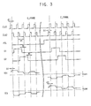
- FIG. 3 is a waveform diagram illustrating signals of the display driving part of FIG. 2 .
- a data driving part 230 receives a first clock signal CLK1, a second clock signal CLK2 and a polarity inversion signal POL from a control circuit part 210, and outputs the data signals YO1, YE1.
- odd-numbered data signals YO1, ..., YOm/2 may be provided to odd-numbered data lines
- even-numbered data signals YE1, ..., YEm/2 may be provided to even-numbered data lines.
- a gate driving part 250 receives the gate control signal GCONT from the control circuit part 210 and outputs gate signals G1, G2.
- the display driving part 200 may be driven by a column inversion mode and a frame inversion mode.
- the first clock signal CLK1 may control a rising time, that is, a start timing of a rising period during which each the odd-numbered data signal YO1 rises from a low level to a high level.
- a rising time that is, a start timing of a rising period during which each the odd-numbered data signal YO1 rises from a low level to a high level.
- each of the data values that is included in the odd-numbered data signal YO1 may be outputted with reference to the first clock signal CLK1 every one horizontal period 1H.
- the data values are changed with reference to a rising edge of the first clock signal CLK1, the invention is not limited thereto.
- the data values of the odd-numbered data signal YO1 in every horizontal period 1H may be outputted in synchronization with a rising edge or a falling edge of the first clock signal CLK1.
- the second clock signal CLK2 may control a rising time, that is, a start timing of a rising period during which the even-numbered data signal YE1 rises from a low level to a high level.
- a rising time that is, a start timing of a rising period during which the even-numbered data signal YE1 rises from a low level to a high level.
- each of the data values which is included in the even-numbered data signal YE1 may be outputted with reference to the second clock signal CLK2 every one horizontal period 1H.
- the data values are changed with reference to a rising edge of the second clock signal CLK2, the invention is not limited thereto.
- the data values of the even-numbered data signal YE1 every one horizontal period 1H may be outputted in synchronization with a rising edge or a falling edge of the second clock signal CLK2.
- the first clock signal CLK1 precedes the second clock signal CLK2 by a predetermined time period ⁇ t.
- the second clock signal CLK2 precedes the first clock signal CLK1 by a predetermined time period ⁇ t.
- a pulse of the first clock signal CLK1 precedes a pulse of the second clock signal CLK2 without overlapping.
- a pulse of the second clock signal CLK2 precedes a pulse of the first clock signal CLK1 without overlapping.
- first pulses of the first clock signal CLK1 during the odd-numbered frame period O_FRAME are out of phase with first pulses of the second clock signal CLK2 during the odd-numbered frame period O_FRAME by a first angle.
- second pulses of the first clock signal CLK1 during the even-numbered frame period E_FRAME are out of phase with second pulses of the second clock signal CLK2 during the even-numbered frame period E_FRAME by a second angle.
- a clock signal (first clock signal CLK1 or second clock signal CLK2) which is synchronized to the data value which has a positive polarity may precede a clock signal (second clock signal CLK2 or first clock signal CLK1) which is synchronized to the data value which has a negative polarity by the predetermined time ⁇ t.
- a data signal which has a positive polarity value may be outputted before a data signal which has a negative polarity value by the predetermined time ⁇ t.
- the predetermined time ⁇ t has a duration that is the same as the duration of one of the pulses of the clock signals.
- the polarity inversion signal POL reverses the data signals YO1, YE1.
- the polarity inversion signal POL may have a low level during the odd-numbered frame period O_FRAME, and have a high level during even-numbered frame period E_FRAME.
- the odd-numbered data signal YO1 has data values which have different polarities in the odd-numbered frame period O_FRAME and the even-numbered frame period E_FRAME.
- the even-numbered data signal YE1 has data values which have different polarities in the odd-numbered frame period O_FRAME and the even-numbered frame period E_FRAME.
- the gate driving part 250 may generate the gate signals G1, G2 which have a gate-on level and a gate-off level using a gate-on signal having a high level and a gate-off signal having a low level.
- Each of the gate signals G1, G2 may be provided to each of the first and second gate lines first during two horizontal periods 2H, in order.
- the falling timing of gate signals G1, G2 may be set by a control period W of an output enable control signal (e.g., refer to OE of FIG. 4B ).
- the odd-numbered data signal YO1 has a positive (+) data value with reference to a reference signal VCOM during the odd-numbered frame period O_FRAME.
- the odd-numbered data signal YO1 has a negative (-) data value with reference to the reference signal VCOM during the even-numbered frame period E_FRAME.
- the even-numbered data signal YE1 has a negative (-) data value with reference to the reference signal VCOM during the odd-numbered frame period O_FRAME.
- the even-numbered data signal YE1 has a positive (+) data value with reference to the reference signal VCOM during the even-numbered frame period E_FRAME.
- a data signal having the positive data value precedes the data signal having the negative data value by the predetermined time ⁇ t, so that a positive data charging time is longer than a negative data charging time by the predetermined time ⁇ t.
- display quality degradation due to a charging ratio difference according to polarities may be reduced.
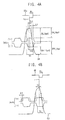
- FIGS. 4A and 4B are waveform diagrams illustrating a data charging ratio according to a gate signal and a data signal.
- FIG. 4A is a waveform diagram illustrating a data charging ratio by a gate signal according to a comparative embodiment.
- FIG. 4B is a waveform diagram illustrating a data charging ratio by a gate signal according to an embodiment of the invention.
- the output-enable control signal controls the falling timing of the gate signal to prevent the data signals applied to adjacent pixel rows from mixing.
- the RC delay time period of the gate signal is increased in an area far away from the gate driving part.
- the output-enable control signal is determined depending on a delay condition of the central area, in which the RC delay time period of the gate signal is largest.
- the output-enable control signal OEc has a control period Wc which controls a falling timing Fc of a gate signal Gd.
- the control period Wc is determined depending on the negative polarity data signal (-) which is a worst case to prevent the data signals of adjacent pixel rows from mixing.
- the positive polarity data signal (+) has a first charging time period Tc1 and the negative polarity data signal (-) has a second charging time period Tc2, by the gate signal Gd having the falling timing which is determined by the control period Wc of the output-enable control signal OEc.
- the second charging time period Tc2 is greater than the first charging time Tc1 by ⁇ t.
- a gate/source voltage ON_Vgs1 of the positive polarity (+) is less than a gate/source voltage ON_Vgs2 of the negative polarity (-).
- an output current Id of the transistor is increased.
- a data charging ratio of the negative polarity (-) is more than a data charging ratio of the positive polarity (+).
- a charging ratio difference between the positive polarity (+) and the negative polarity (-) causes a lower-quality display with a flicker or an after-image.
- the gate/source voltage OFF_Vgs1 of the positive polarity (+) is different from the gate/source voltage OFF_Vgs2 of the negative polarity (-) so that a turn-off period of the positive polarity (+) is different from that of the negative polarity (-), in a voltage-current curve of a transistor. Therefore, an off-leakage current of the positive polarity (+) is different from an off-leakage current of the negative polarity (-), so that an off-leakage current difference causes a lower-quality display with a flicker or an after-image.
- the positive polarity data signal (+) precedes the negative polarity data signal (-) by a predetermined time ⁇ t.
- the output-enable control signal OE has a control period W which controls a falling timing F of a gate signal Gd.
- the control period W is determined depending on the negative polarity data signal (-) which is a worst case to prevent the data signals of adjacent pixel rows from mixing.
- the positive polarity data signal (+) has a first charging time period T1
- the negative polarity data signal (-) has a second charging time period T2, by the gate signal Gd which corresponds to the control period of the output-enable control signal OE. Since the positive polarity data signal (+) precedes the negative polarity data signal (-) by the predetermined time ⁇ t, the positive polarity data signal (+) has a charging time that is longer than that of FIG. 4A by the predetermined time ⁇ t. Thus, display quality degradation due to charging ratio differences according to polarities may be reduced.
- FIG. 5 is a graph illustrating set-up of a control time of an output enable signal and a predetermined time which is a difference of output timings of data signals.
- the graph has an x-axis which means time, and a y-axis which means voltage V.
- An ideal gate signal G and a delayed gate signal Gd are illustrated.
- An RC delay value GRC of a gate signal may be calculated by a traditional method.
- a predetermined time (refers to ⁇ t of FIG. 4B ) which is a time interval of the positive polarity data signal(+) and the negative polarity data signal (-) may be set according to the RC delay value GRC, a reference voltage, a voltage range of a positive polarity data signal (+), and a voltage range of a negative polarity data signal (-).
- the predetermined time is proportional to the RC delay value GRC.
- an output-enable control signal (refer to OE of FIG. 4B ) may be set based on the negative polarity data signal (-), or based on the positive polarity data signal (+).
- the positive polarity data signal (+) has more charging time as a difference between dt1 and dt2, is about 30% of the RC delay value GRC.
- the difference between dt1 and dt2 is the same as the predetermined time.
- FIG. 6 is a waveform diagram illustrating signals of a display driving part according to an embodiment of the invention.
- a data driving part 230 outputs the data signals YO1, YE1 based on the first clock signal CLK1, the second clock signal CLK2 and the polarity inversion signal POL from a control circuit part 210.
- odd-numbered data signal YO1 may be provided to odd-numbered data lines and even-numbered data signal YE1 may be provided to even-numbered data lines.
- the gate driving part 250 receives the gate control signal GCONT from a control circuit part 210 and outputs gate signals G1, G2.
- the display driving part may be driven by a column inversion mode and a frame inversion mode.
- the first clock signal CLK1 may control a rising time, that is, a start timing of a rising period during which each of the odd-numbered data signals YO1 rise from a low level to a high level.
- a rising time that is, a start timing of a rising period during which each of the odd-numbered data signals YO1 rise from a low level to a high level.
- the each of the data values which is included in the odd-numbered data signal YO1 may be outputted with reference to the first clock signal CLK1 every one horizontal period 1H.
- the data values are changed with reference to a rising edge of the first clock signal CLK1, the invention is not limited thereto.
- the data values of the odd-numbered data signal YO1 every one horizontal period 1H may be outputted in synchronization with a rising edge or a falling edge of the first clock signal CLK1.
- the second clock signal CLK2 may control a rising time, that is, a start timing of a rising period during which the even-numbered data signal YE1 rises from a low level to a high level.
- a rising time that is, a start timing of a rising period during which the even-numbered data signal YE1 rises from a low level to a high level.
- each of the data values which is included in the even-numbered data signal YE1 may be outputted with reference to the second clock signal CLK2 every one horizontal period 1H.
- the data values are changed with reference to a rising edge of the second clock signal CLK2, the invention is not limited thereto.
- the data values of the even-numbered data signal YE1 every one horizontal period 1H may be outputted in synchronization with a rising edge or a falling edge of the second clock signal CLK2.
- the second clock signal CLK2 follows the first clock signal CLK1 by a predetermined time ⁇ t.
- a pulse of the second clock signal CLK2 follows and partially overlaps a pulse of the first clock signal CLK1.
- first pulses of the first clock signal CLK1 during the odd-numbered frame period O_FRAME are out of phase with first pulses of the second clock signal CLK2 during the odd-numbered frame period O_FRAME by a first angle.
- the first clock signal CLK1 follows the second clock signal CLK2 by a predetermined time ⁇ t.
- a pulse of the first clock signal CLK1 follows and partially overlaps a pulse of the second clock signal CLK2.
- second pulses of the first clock signal CLK1 during the even-numbered frame period E_FRAME are out of phase with second pulses of the second clock signal CLK2 during the even-numbered frame period E_FRAME by a second angle.
- a clock signal (second clock signal CLK2 or first clock signal CLK1) which is synchronized to the data value which has a negative polarity follows a clock signal (first clock signal CLK1 or second clock signal CLK2) which is synchronized to the data value which has a positive polarity by the predetermined time ⁇ t.
- a data signal which has a negative polarity value may be outputted next to a data signal which has positive polarity value by the predetermined time ⁇ t.
- the polarity inversion signal POL reverses the data signals YO1, YE1.
- the polarity inversion signal POL may have a low level during the odd-numbered frame period O_FRAME, and have a high level during the even-numbered frame period E_FRAME.
- the odd-numbered data signal YO1 has data values which have different polarities in the odd-numbered frame period O_FRAME and the even-numbered frame period E_FRAME.
- the even-numbered data signal YE1 has data values which have different polarities in the odd-numbered frame period O_FRAME and the even-numbered frame period E_FRAME.
- the gate driving part 250 may generate the gate signal G1, G2 which have a gate-on level and a gate-off level using a gate-on signal having a high level and a gate-off signal having a low level.
- Each of the gate signals G1, G2 may be provided to each of the first and second gate lines first during two horizontal periods 2H, in order.
- the falling timing of gate signals G1, G2 may be set by a control period W of an output enable control signal (e.g., refers to OE of FIG. 4B ).
- the output enable control signal is set with reference to a negative polarity data signal, so that the control period W is set in consideration of the predetermined time ⁇ t.
- the odd-numbered data signal YO1 may have a positive (+) data value with reference to a reference signal VCOM during the odd-numbered frame period O_FRAME.
- the odd-numbered data signal YO1 may have a negative (-) data value with reference to the reference signal VCOM during the even-numbered frame period E_FRAME.
- the even-numbered data signal YE1 may have a negative (-) data value with reference to the reference signal VCOM during the odd-numbered frame period O_FRAME.
- the even-numbered data signal YE1 may have a positive (+) data value with reference to the reference signal VCOM during the even-numbered frame period E_FRAME.
- a data signal having a negative data value follows a data signal having a positive data value by the predetermined time ⁇ t, so that a positive data charging time is longer than a negative data charging time by the predetermined time ⁇ t.
- display quality degradation due to charging ratio differences according to polarities may be reduced.
- FIG. 7 is a waveform diagram illustrating signals of a display driving part according to an embodiment of the invention.
- a data driving part 230 may output the data signals YO1, YE1 based on the first clock signal CLK1, the second clock signal CLK2 and the polarity inversion signal POL from a control circuit part 210.
- odd-numbered data signal YO1 may be provided to odd-numbered data lines and even-numbered data signal YE1 may be provided to even-numbered data lines.
- the gate driving part 250 may receive the gate control signal GCONT from the control circuit part 210 and output gate signals G1, G2.
- the display driving part may be driven by a column inversion mode and a frame inversion mode.
- the first clock signal CLK1 precedes the second clock signal CLK2 by a predetermined time ⁇ t.
- pulses of the first clock signal CLK1 precede respective pulses of the second clock signal CLK2 in the odd-numbered frame period O_FRAME and the even-numbered frame period E_FRAME.
- the first clock signal CLK1 may control output timing of data signal which includes positive polarity data values.
- the second clock signal CLK2 may control output timing of data signals which includes negative polarity data value.
- each of the data values of the odd-numbered data signal YO1 may be outputted with reference to the first clock signal CLK1 every one horizontal period 1H.
- each of the data values of the even-numbered data signal YE1 are outputted with reference to the second clock signal CLK2 every one horizontal period 1H.
- each of the data values of the odd-numbered data signal YO1 may be outputted with reference to the second clock signal CLK2 every one horizontal period 1H.
- each of the data values of the even-numbered data signal YE1 is outputted with reference to the first clock signal CLK1 every one horizontal period 1H.
- the data values are changed with reference to a rising edge of the second clock signal CLK2, the invention is not limited thereto.
- the data values of the even-numbered data signal YE1 every one horizontal period 1H may be outputted in synchronization with a rising edge or a falling edge of the second clock signal CLK2.
- the polarity inversion signal POL reverses the data signals YO1, YE1.
- the polarity inversion signal POL may have a low level during the odd-numbered frame period O_FRAME, and have a high level during even-numbered frame period E_FRAME.
- the odd-numbered data signal YO1 may have data values which have different polarities in the odd-numbered frame period O_FRAME and the even-numbered frame period E_FRAME.
- the even-numbered data signal YE1 may have data values which have different polarities in the odd-numbered frame period O_FRAME and the even-numbered frame period E_FRAME.
- first and second clock signals CLK1, CLK2 may be synchronized to the odd or even-numbered data signal YO1, YE1 based on the polarity inversion signal POL. For example, during the odd-numbered frame period O_FRAME, when the polarity inversion signal POL has the low level, the first clock signal CLK1 is synchronized to the odd-numbered data signal YO1, and the second clock signal CLK2 is synchronized to the even-numbered data signal YE1.
- the first clock signal CLK1 is synchronized to the even-numbered data signal YE1
- the second clock signal CLK2 is synchronized to the odd-numbered data signal YO1.
- the gate driving part 250 may generate the gate signal G1, G2 which have gate-on level and gate-off level using a gate-on signal having a high level and a gate-off signal having a low level.
- Each of the gate signals G1, G2 may be provided to each of the first and second gate lines first during two horizontal periods 2H, in order.
- the falling timing of gate signals G1, G2 may be set by a control period W of an output enable control signal (e.g., refer to OE of FIG. 4B ).
- the odd-numbered data signal YO1 may have a positive (+) data value with reference to a reference signal VCOM during the odd-numbered frame period O_FRAME.
- the odd-numbered data signal YO1 may have a negative (-) data value with reference to the reference signal VCOM during the even-numbered frame period E_FRAME.
- the even-numbered data signal YE1 may have a negative (-) data value with reference to the reference signal VCOM during the odd-numbered frame period O_FRAME.
- the even-numbered data signal YE1 may have a positive (+) data value with reference to the reference signal VCOM during the even-numbered frame period E_FRAME.
- a data signal having the negative data value follows a data signal having a positive data value by the predetermined time ⁇ t, so that positive data charging time is longer than negative data charging time by the predetermined time ⁇ t.
- display quality degradation due to charging ratio differences according to polarities may be reduced.
- output timing of positive polarity data signals and output timing of negative polarity data signals may be different from each other, so that display quality degradation due to charging ratio differences between positive and negative polarities according to an RC delay of a scan signal (e.g., a gate signal) may be reduced.
- a scan signal e.g., a gate signal
Landscapes
- Engineering & Computer Science (AREA)
- Physics & Mathematics (AREA)
- Computer Hardware Design (AREA)
- General Physics & Mathematics (AREA)
- Theoretical Computer Science (AREA)
- Chemical & Material Sciences (AREA)
- Crystallography & Structural Chemistry (AREA)
- Control Of Indicators Other Than Cathode Ray Tubes (AREA)
Abstract
Description
- Embodiments of the invention relate to a method of driving a display panel and a display apparatus for performing the method.
- A liquid crystal display (LCD) apparatus is typically thin, light and uses very little power consumption. Thus the LCD apparatus is used in monitors, laptop computers and cellular phones. The LCD apparatus includes an LCD panel displaying images using a light transmittance of a liquid crystal, a backlight assembly disposed under the LCD panel that provides light to the LCD panel and a driving circuit driving the LCD panel.
- The liquid display panel includes an array substrate having gate lines, data lines, pixels and an opposing substrate, which has a common electrode. A liquid crystal layer is disposed between the array substrate and the opposing substrate. The driving circuit includes a gate driving part that drives the gate lines with gate signals and a data driving part that drives the data lines with data signals.
- However, a RC time delay of the gate signal transferred through a gate line and the data signal transferred through a data line occurs when a liquid display panel has a large size. For example, the RC time delay of the gate signal occurs in an area far away from the gate driving part outputting the gate signal the gate driving part. The gate signal controls a charging period during which the data signal is charged in the pixel so that a charging ratio may be decreased by the RC time delay of the gate signal. The RC time delay may reduce the quality of the display panel. For example, luminance lowering, color mixing, and ghosting may be caused by the RC time delay.
- At least one embodiment of the invention sets out to provide a method of driving a display panel that is capable of decreasing a data charging ratio difference by a delay of a gate signal.
- At least one embodiment of the invention sets out to provide a display apparatus that performs a method of driving the display panel.
- According to an embodiment of the invention, a method of driving a display panel includes providing a positive polarity data signal to a first data line during an odd-numbered frame, and providing a negative polarity data signal to the first data line during an even-numbered frame. The positive polarity data signal has a first polarity. The negative polarity data signal has a second polarity. Output timing of the positive polarity data signal is different from output timing of the negative polarity data signal.
- In an embodiment of the invention, the output timing of the positive polarity data signal precedes the output timing of the negative polarity data signal by a predetermined time period.
- In an embodiment of the invention, during the odd-numbered frame, a negative polarity data signal having the second polarity is provided to a second data line which is adjacent to the first data line, and during the even-numbered frame, a positive polarity data signal having the first polarity is provided to the second data line.
- In an embodiment of the invention, the predetermined time period is shorter than one horizontal period.
- In an embodiment of the invention, the predetermined time period is set to be proportional to a RC delay time period of a gate signal.
- In an embodiment of the invention, the predetermined time period is about 30% of an RC delay time period of a gate signal.
- In an embodiment of the invention, the method further includes generating a first clock signal, and generating a second clock signal, where the first clock signal and the second clock signal have rising times different from each other.
- In an embodiment of the invention, during the odd-numbered frame, the first clock signal controls the output timing of data signal which is provided to the first data line, and during the even-numbered frame, the second clock signal controls the output timing of a data signal which is provided to the second data line.
- In an embodiment of the invention, the first clock signal controls the output timing of the positive polarity data signal, and the second clock signal controls the output timing of the negative polarity data signal.
- According to an embodiment of the invention, a display apparatus includes a display panel including a plurality of data lines, a plurality of gate lines and a plurality of pixels, a data driver configured to provide a positive polarity data signal and a negative polarity data signal to the display panel. Each of the pixels includes a switching element electrically connected to a corresponding one of the gate lines and a corresponding one of the data lines. The positive polarity data signal has a first polarity. The negative polarity data signal has a second polarity. Output timing of the positive polarity data signal is different from output timing of the negative polarity data.
- In an embodiment of the invention, the output timing of the positive polarity data signal precedes the output timing of the negative polarity data signal by a predetermined time period.
- In an embodiment of the invention, the positive polarity data signal is provided to a first data line among the data lines during an odd-numbered frame, and the negative polarity data signal is provided to the first data line during an even-numbered frame.
- In an exemplary embodiment, the data driver is configured to control output timing of the first data line using a first clock signal, and configured to control output timing of a second data line using a second clock signal.
- In an embodiment of the invention, the data driver is configured to control output timing of the positive polarity data signal using a first clock signal, and configured to control output timing of a negative polarity data signal using a second clock signal.
- In an embodiment of the invention, a second negative polarity data signal having the second polarity is provided to a second data line among the data lines during an odd-numbered frame, and a second positive polarity data signal having the first polarity is provided to the second data line during an even-numbered frame.
- In an embodiment of the invention, the data driver is configured to control output timing of the first data line using a first clock signal, and configured to control output timing of a second data line using a second clock signal, where the second clock signal has a rising edge different from that of the first clock signal.
- In an embodiment of the invention, the predetermined time period is shorter than one horizontal period.
- In an embodiment of the invention, the predetermined time period is set to be proportional to an RC delay time period of a gate signal.
- In an embodiment of the invention, the predetermined time period is about 30% of an RC delay time period of a gate signal.
- In an embodiment of the invention, during one frame, data signals having a same polarity are provided to a same data line.
- According to an embodiment of the invention, a driving apparatus for a display panel of a display apparatus includes a controller circuit configured to output a first clock signal with a first timing and a second clock signal with a second different timing; and a data driving circuit configured to provide a positive polarity data signal having a first polarity to a first data line of the display panel in response to the first clock signal, and provide a negative polarity data signal having a second polarity to a second adjacent data line of the display panel in response to the second clock signal.
- In an embodiment of the invention, pulses of the second clock signal follow respective pulses of the first clock signal without overlap during an odd-numbered frame period, and pulses of the second clock signal precede respective pulses of the first clock signal without overlap during an even-numbered frame period.
- In an embodiment of the invention, wherein pulses of the second clock signal follow respective pulses of the first clock signal with overlap during an odd-numbered frame period, and pulses of the second clock signal precede respective pulses of the first clock signal with overlap during an even-numbered frame period,
- In an embodiment of the invention, wherein pulses of the second clock signal follow respective pulses of the first clock signal without overlap.
- At least some of the above and other features of the invention are set out in the claims.
- According to embodiments of the invention, output timing of a positive polarity data signal and output timing of a negative polarity data signal may be different each other, so that display quality degradation due to a charging ratio difference between positive and negative polarities according to an RC delay of a scan signal may be reduced.
- The invention will become more apparent by describing in detail embodiments thereof with reference to the accompanying drawings, in which:
-
FIG. 1 is a plan view illustrating a display panel according to an embodiment of the invention; -
FIG. 2 is a block diagram illustrating a display driving part ofFIG. 1 according to an embodiment of the invention; -
FIG. 3 is a waveform diagram illustrating signals of the display driving part ofFIG. 2 ; -
FIGS. 4A and 4B are waveform diagrams illustrating a data charging ratio according to a gate signal and a data signal; -
FIG. 5 is a graph illustrating set-up of a control time of an output enable signal and a predetermined time which is a difference of output timings of data signals according to an exemplary embodiment of the invention; -
FIG. 6 is a waveform diagram illustrating signals of a display driving part according to an exemplary embodiment of the inventive concept; and -
FIG. 7 is a waveform diagram illustrating signals of a display driving part according to an exemplary embodiment of the invention. - Hereinafter, embodiments of the invention will be explained in detail with reference to the accompanying drawings.
-
FIG. 1 is a plan view illustrating a display panel according to an embodiment of the invention.FIG. 2 is a block diagram illustrating a display driving part ofFIG. 1 . - Referring to
FIGS. 1 and2 , the display panel includes adisplay panel 100 and a display driving part 200 (e.g., a driver or a driver circuit). - The
display panel 100 includes a plurality of data lines DL1, ..., DLm, a plurality of gate lines GL1, ..., GLn and a plurality of pixels P. Each of the pixels P includes a switching element TR connected to a data line DL1 and a gate line GL1 and a liquid crystal capacitor CLC connected to the switching element TR. - The pixels P are arranged as a matrix type which includes a plurality of pixel rows and a plurality of pixel columns. The data lines DL1, ..., DLm are extended in a first direction D1, that is a column direction, and arranged in a second direction D2, that is, a row direction, crossing the first direction D1. Each of the data lines is electrically connected to the pixels of a same pixel column arranged in the first direction D1.
- The gate lines GL1, ..., GLn are extended in the second direction D2 and arranged in the first direction D1. Each of the gate lines is electrically connected to the pixels of a same pixel row arranged in the second direction D2.
- The
display driving part 200 includes a control circuit part 210 (e.g., a controller or a control circuit), a data driving part 230 (e.g., a data/source driver or a data/source driver circuit) and a gate driving part 250 (e.g., a gate/scan driver or gate/scan driver circuit). Thecontrol circuit part 210 controls operation of thedata driving part 230. In an embodiment thecontrol circuit part 210 is incorporated within a timing controller. - For example, the
control circuit part 210 provides thedata driving part 230 with at least one of a data signal DATA and a data control signal. In an embodiment, the data signal DATA includes a color data signal and may be a signal corrected using compensation algorithms for improving a response time of liquid crystal and for compensating a white. - In an embodiment, the data control signal includes a first clock signal CLK1, a second clock signal CLK2 and a polarity inversion signal POL.
- The
data driving part 230 provides data signals YO1, YE1, ...,YOm/2, YEm/2 to the data lines DL1, ..., DLm according to a column inversion mode. Thedata driving part 230 outputs the data signals YO1, YE1, ...,YOm/2, YEm/2 based on the first clock signal CLK1, the second clock signal CLK2 and the polarity inversion signal POL. - For example, the
data driving part 230 may provide data signals having polarities different from each other to adjacent data lines. In an embodiment, the data signals have different polarities each one frame period. In an embodiment, one frame period is a period during which data signals are output an entire group of pixel rows (e.g., all odd pixel rows or all even pixel rows). Thus, odd-numbered data signals YO1, ..., YOm/2 may be provided to odd-numbered data lines (e.g., D1, D3, etc.) and even-numbered data signal YE1, ..., YEm/2 may be provided to even-numbered data lines (e.g., D2, D4, etc.). The odd-numbered data signals YO1, ..., YOm/2 may have first polarity or second polarity with respect to reference signal according to the polarity inversion signal POL. The even-numbered data signals YE1, ... , YEm/2 may have first polarity or second polarity with respect to the reference signal according to the polarity inversion signal POL. The polarity inversion signal POL may have different value in every frame. For example, the voltage level of the polarity inversion signal POL may toggle between first and a second different logic levels each next frame period. Accordingly, thedisplay panel 100 may be driven by a column inversion mode and a frame inversion mode. - In an embodiment of the invention, the
control circuit part 210 controls thegate driving part 250. - In an embodiment of the invention, the
control circuit part 210 provides a gate control signal GCONT to thegate driving part 250. - The
gate driving part 250 may include a plurality of shift resistors which generate gate signals G1, G2, G3, ..., Gn. Thegate driving part 250 receives the gate control signal GCONT from thecontrol circuit part 210. The gate control signal GCONT may include a gate on signal, a gate off signal, a vertical start signal, a gate clock signal, an output enable signal (e.g., refer to OE ofFIG. 4B ). - The vertical start signal may control a start timing at which an operation of the
gate driving part 250 is started. The gate clock signal may control a rising timing, that is, a start timing of a rising period during which each of the gate signals G1, ..., Gn rises from a low level to a high level. The output enable control signal OE may control a falling timing, that is, a start timing of a falling period during which each of the gate signals G1, ..., Gn falls from the high level to the low level. - The gate on signal may control a gate-on level (or voltage) of the gate signals G1, ..., Gn and the gate-off signal (or voltage) may control a gate-off level of the gate signals G1, ..., Gn. In an embodiment, the level of the gate-on signal differs from the level of the gate-off signal.
-
FIG. 3 is a waveform diagram illustrating signals of the display driving part ofFIG. 2 . - Referring to
FIGS. 2 and3 , adata driving part 230 receives a first clock signal CLK1, a second clock signal CLK2 and a polarity inversion signal POL from acontrol circuit part 210, and outputs the data signals YO1, YE1. Thus, odd-numbered data signals YO1, ..., YOm/2 may be provided to odd-numbered data lines, and even-numbered data signals YE1, ..., YEm/2 may be provided to even-numbered data lines. Agate driving part 250 receives the gate control signal GCONT from thecontrol circuit part 210 and outputs gate signals G1, G2. Thedisplay driving part 200 may be driven by a column inversion mode and a frame inversion mode. - For convenience of explanation, only gate signals G1, G2 for first and second gate lines, and odd-numbered data signal YO1 and even-numbered data signal YE1 will be explained.
- The first clock signal CLK1 may control a rising time, that is, a start timing of a rising period during which each the odd-numbered data signal YO1 rises from a low level to a high level. Thus, each of the data values that is included in the odd-numbered data signal YO1 may be outputted with reference to the first clock signal CLK1 every one
horizontal period 1H. - In addition, although the data values are changed with reference to a rising edge of the first clock signal CLK1, the invention is not limited thereto. For example, the data values of the odd-numbered data signal YO1 in every
horizontal period 1H may be outputted in synchronization with a rising edge or a falling edge of the first clock signal CLK1. - The second clock signal CLK2 may control a rising time, that is, a start timing of a rising period during which the even-numbered data signal YE1 rises from a low level to a high level. Thus, each of the data values which is included in the even-numbered data signal YE1 may be outputted with reference to the second clock signal CLK2 every one
horizontal period 1H. - In addition, although the data values are changed with reference to a rising edge of the second clock signal CLK2, the invention is not limited thereto. For example, the data values of the even-numbered data signal YE1 every one
horizontal period 1H may be outputted in synchronization with a rising edge or a falling edge of the second clock signal CLK2. - During an odd-numbered frame period O_FRAME, the first clock signal CLK1 precedes the second clock signal CLK2 by a predetermined time period Δt. During an even-numbered frame period E_FRAME, the second clock signal CLK2 precedes the first clock signal CLK1 by a predetermined time period Δt. In an embodiment, during part of the odd-numbered frame period O_FRAME, a pulse of the first clock signal CLK1 precedes a pulse of the second clock signal CLK2 without overlapping. In an embodiment, during part of the even-numbered frame period E_FRAME, a pulse of the second clock signal CLK2 precedes a pulse of the first clock signal CLK1 without overlapping. In an embodiment, first pulses of the first clock signal CLK1 during the odd-numbered frame period O_FRAME are out of phase with first pulses of the second clock signal CLK2 during the odd-numbered frame period O_FRAME by a first angle. In an embodiment, second pulses of the first clock signal CLK1 during the even-numbered frame period E_FRAME are out of phase with second pulses of the second clock signal CLK2 during the even-numbered frame period E_FRAME by a second angle.
- A clock signal (first clock signal CLK1 or second clock signal CLK2) which is synchronized to the data value which has a positive polarity may precede a clock signal (second clock signal CLK2 or first clock signal CLK1) which is synchronized to the data value which has a negative polarity by the predetermined time Δt. Thus, a data signal which has a positive polarity value may be outputted before a data signal which has a negative polarity value by the predetermined time Δt. In an embodiment, the predetermined time Δt has a duration that is the same as the duration of one of the pulses of the clock signals.
- In an embodiment of the invention, the polarity inversion signal POL reverses the data signals YO1, YE1. For example, the polarity inversion signal POL may have a low level during the odd-numbered frame period O_FRAME, and have a high level during even-numbered frame period E_FRAME. Accordingly, the odd-numbered data signal YO1 has data values which have different polarities in the odd-numbered frame period O_FRAME and the even-numbered frame period E_FRAME. The even-numbered data signal YE1 has data values which have different polarities in the odd-numbered frame period O_FRAME and the even-numbered frame period E_FRAME.
- The
gate driving part 250 may generate the gate signals G1, G2 which have a gate-on level and a gate-off level using a gate-on signal having a high level and a gate-off signal having a low level. Each of the gate signals G1, G2 may be provided to each of the first and second gate lines first during two horizontal periods 2H, in order. The falling timing of gate signals G1, G2 may be set by a control period W of an output enable control signal (e.g., refer to OE ofFIG. 4B ). - The odd-numbered data signal YO1 has a positive (+) data value with reference to a reference signal VCOM during the odd-numbered frame period O_FRAME. The odd-numbered data signal YO1 has a negative (-) data value with reference to the reference signal VCOM during the even-numbered frame period E_FRAME.
- The even-numbered data signal YE1 has a negative (-) data value with reference to the reference signal VCOM during the odd-numbered frame period O_FRAME. The even-numbered data signal YE1 has a positive (+) data value with reference to the reference signal VCOM during the even-numbered frame period E_FRAME.
- According to the present embodiment, a data signal having the positive data value precedes the data signal having the negative data value by the predetermined time Δt, so that a positive data charging time is longer than a negative data charging time by the predetermined time Δt. Thus, display quality degradation due to a charging ratio difference according to polarities may be reduced.
-
FIGS. 4A and 4B are waveform diagrams illustrating a data charging ratio according to a gate signal and a data signal. -
FIG. 4A is a waveform diagram illustrating a data charging ratio by a gate signal according to a comparative embodiment.FIG. 4B is a waveform diagram illustrating a data charging ratio by a gate signal according to an embodiment of the invention. - Generally, the output-enable control signal controls the falling timing of the gate signal to prevent the data signals applied to adjacent pixel rows from mixing. The RC delay time period of the gate signal is increased in an area far away from the gate driving part. For example, when the gate driving part is respectively disposed in areas adjacent to both ends of the gate line, such as a dual-bank structure, the RC delay time period of the gate signal is largest in a central area of the display panel in a horizontal direction. Therefore, the output-enable control signal is determined depending on a delay condition of the central area, in which the RC delay time period of the gate signal is largest.
- Referring to
FIG. 4A , according to the comparative embodiment, the output-enable control signal OEc has a control period Wc which controls a falling timing Fc of a gate signal Gd. The control period Wc is determined depending on the negative polarity data signal (-) which is a worst case to prevent the data signals of adjacent pixel rows from mixing. - Thus, the positive polarity data signal (+) has a first charging time period Tc1 and the negative polarity data signal (-) has a second charging time period Tc2, by the gate signal Gd having the falling timing which is determined by the control period Wc of the output-enable control signal OEc. The second charging time period Tc2 is greater than the first charging time Tc1 by Δt.
- In other words, a gate/source voltage ON_Vgs1 of the positive polarity (+) is less than a gate/source voltage ON_Vgs2 of the negative polarity (-). When the gate/source voltage Vgs is increased, an output current Id of the transistor is increased. Thus, a data charging ratio of the negative polarity (-) is more than a data charging ratio of the positive polarity (+). As described above, a charging ratio difference between the positive polarity (+) and the negative polarity (-) causes a lower-quality display with a flicker or an after-image.
- In addition, the gate/source voltage OFF_Vgs1 of the positive polarity (+) is different from the gate/source voltage OFF_Vgs2 of the negative polarity (-) so that a turn-off period of the positive polarity (+) is different from that of the negative polarity (-), in a voltage-current curve of a transistor. Therefore, an off-leakage current of the positive polarity (+) is different from an off-leakage current of the negative polarity (-), so that an off-leakage current difference causes a lower-quality display with a flicker or an after-image.
- Referring to
FIG. 4B , according to an embodiment of the invention, the positive polarity data signal (+) precedes the negative polarity data signal (-) by a predetermined time Δt. - The output-enable control signal OE has a control period W which controls a falling timing F of a gate signal Gd. The control period W is determined depending on the negative polarity data signal (-) which is a worst case to prevent the data signals of adjacent pixel rows from mixing.
- Accordingly, the positive polarity data signal (+) has a first charging time period T1, and the negative polarity data signal (-) has a second charging time period T2, by the gate signal Gd which corresponds to the control period of the output-enable control signal OE. Since the positive polarity data signal (+) precedes the negative polarity data signal (-) by the predetermined time Δt, the positive polarity data signal (+) has a charging time that is longer than that of
FIG. 4A by the predetermined time Δt. Thus, display quality degradation due to charging ratio differences according to polarities may be reduced. -
FIG. 5 is a graph illustrating set-up of a control time of an output enable signal and a predetermined time which is a difference of output timings of data signals. - Referring to
FIG. 5 , the graph has an x-axis which means time, and a y-axis which means voltage V. An ideal gate signal G and a delayed gate signal Gd are illustrated. - An RC delay value GRC of a gate signal may be calculated by a traditional method. A predetermined time (refers to Δt of
FIG. 4B ) which is a time interval of the positive polarity data signal(+) and the negative polarity data signal (-) may be set according to the RC delay value GRC, a reference voltage, a voltage range of a positive polarity data signal (+), and a voltage range of a negative polarity data signal (-). - In an embodiment of the invention, the predetermined time is proportional to the RC delay value GRC.
- In addition, an output-enable control signal (refer to OE of
FIG. 4B ) may be set based on the negative polarity data signal (-), or based on the positive polarity data signal (+). - For example, when voltage range of the positive polarity data signal (+) is 8V to 15V and voltage range of the negative polarity data signal (-) is 0V to 7V, a control period of the output-enable control signal (refer to W of
FIG. 4B ) may be set to 0.7 * RC delay value GRC = dt1 by calculating with reference to a reference time when the negative polarity data signal (-) is 0V (white for normally black mode). - In this example, 0.4 * RC delay value GRC = dt2 may be calculated with reference to a reference time when the positive polarity data signal (+) is 8V (black for normally black mode). Thus, the positive polarity data signal (+) has more charging time as a difference between dt1 and dt2, is about 30% of the RC delay value GRC. In an embodiment, the difference between dt1 and dt2 is the same as the predetermined time.
-
FIG. 6 is a waveform diagram illustrating signals of a display driving part according to an embodiment of the invention. - Referring to
FIGS. 2 and6 , adata driving part 230 outputs the data signals YO1, YE1 based on the first clock signal CLK1, the second clock signal CLK2 and the polarity inversion signal POL from acontrol circuit part 210. Thus, odd-numbered data signal YO1 may be provided to odd-numbered data lines and even-numbered data signal YE1 may be provided to even-numbered data lines. Thegate driving part 250 receives the gate control signal GCONT from acontrol circuit part 210 and outputs gate signals G1, G2. The display driving part may be driven by a column inversion mode and a frame inversion mode. - For convenience of explanation, only gate signals G1, G2 for first and second gate lines, and odd-numbered data signal YO1 and even-numbered data signal YE1 will be explained.
- The first clock signal CLK1 may control a rising time, that is, a start timing of a rising period during which each of the odd-numbered data signals YO1 rise from a low level to a high level. Thus, the each of the data values which is included in the odd-numbered data signal YO1 may be outputted with reference to the first clock signal CLK1 every one
horizontal period 1H. - In addition, although the data values are changed with reference to a rising edge of the first clock signal CLK1, the invention is not limited thereto. For example, the data values of the odd-numbered data signal YO1 every one
horizontal period 1H may be outputted in synchronization with a rising edge or a falling edge of the first clock signal CLK1. - The second clock signal CLK2 may control a rising time, that is, a start timing of a rising period during which the even-numbered data signal YE1 rises from a low level to a high level. Thus, each of the data values which is included in the even-numbered data signal YE1 may be outputted with reference to the second clock signal CLK2 every one
horizontal period 1H. - In addition, although the data values are changed with reference to a rising edge of the second clock signal CLK2, the invention is not limited thereto. For example, the data values of the even-numbered data signal YE1 every one
horizontal period 1H may be outputted in synchronization with a rising edge or a falling edge of the second clock signal CLK2. - During an odd-numbered frame period O_FRAME, the second clock signal CLK2 follows the first clock signal CLK1 by a predetermined time Δt. For example, during part of an odd-numbered frame period O_FRAME, a pulse of the second clock signal CLK2 follows and partially overlaps a pulse of the first clock signal CLK1. In an embodiment, first pulses of the first clock signal CLK1 during the odd-numbered frame period O_FRAME are out of phase with first pulses of the second clock signal CLK2 during the odd-numbered frame period O_FRAME by a first angle. During an even-numbered frame period E_FRAME, the first clock signal CLK1 follows the second clock signal CLK2 by a predetermined time Δt. For example, during part of the even-numbered frame E_FRAME, a pulse of the first clock signal CLK1 follows and partially overlaps a pulse of the second clock signal CLK2. In an embodiment, second pulses of the first clock signal CLK1 during the even-numbered frame period E_FRAME are out of phase with second pulses of the second clock signal CLK2 during the even-numbered frame period E_FRAME by a second angle.
- Thus, a clock signal (second clock signal CLK2 or first clock signal CLK1) which is synchronized to the data value which has a negative polarity follows a clock signal (first clock signal CLK1 or second clock signal CLK2) which is synchronized to the data value which has a positive polarity by the predetermined time Δt. Thus, a data signal which has a negative polarity value may be outputted next to a data signal which has positive polarity value by the predetermined time Δt.
- The polarity inversion signal POL reverses the data signals YO1, YE1. For example, the polarity inversion signal POL may have a low level during the odd-numbered frame period O_FRAME, and have a high level during the even-numbered frame period E_FRAME. Accordingly, the odd-numbered data signal YO1 has data values which have different polarities in the odd-numbered frame period O_FRAME and the even-numbered frame period E_FRAME. The even-numbered data signal YE1 has data values which have different polarities in the odd-numbered frame period O_FRAME and the even-numbered frame period E_FRAME.
- The
gate driving part 250 may generate the gate signal G1, G2 which have a gate-on level and a gate-off level using a gate-on signal having a high level and a gate-off signal having a low level. Each of the gate signals G1, G2 may be provided to each of the first and second gate lines first during two horizontal periods 2H, in order. The falling timing of gate signals G1, G2 may be set by a control period W of an output enable control signal (e.g., refers to OE ofFIG. 4B ). - In an embodiment of the invention, the output enable control signal is set with reference to a negative polarity data signal, so that the control period W is set in consideration of the predetermined time Δt.
- The odd-numbered data signal YO1 may have a positive (+) data value with reference to a reference signal VCOM during the odd-numbered frame period O_FRAME. The odd-numbered data signal YO1 may have a negative (-) data value with reference to the reference signal VCOM during the even-numbered frame period E_FRAME.
- The even-numbered data signal YE1 may have a negative (-) data value with reference to the reference signal VCOM during the odd-numbered frame period O_FRAME. The even-numbered data signal YE1 may have a positive (+) data value with reference to the reference signal VCOM during the even-numbered frame period E_FRAME.
- According to the present embodiment of the invention, a data signal having a negative data value follows a data signal having a positive data value by the predetermined time Δt, so that a positive data charging time is longer than a negative data charging time by the predetermined time Δt. Thus, display quality degradation due to charging ratio differences according to polarities may be reduced.
-
FIG. 7 is a waveform diagram illustrating signals of a display driving part according to an embodiment of the invention. - Referring to
FIGS. 2 and7 , adata driving part 230 may output the data signals YO1, YE1 based on the first clock signal CLK1, the second clock signal CLK2 and the polarity inversion signal POL from acontrol circuit part 210. Thus, odd-numbered data signal YO1 may be provided to odd-numbered data lines and even-numbered data signal YE1 may be provided to even-numbered data lines. Thegate driving part 250 may receive the gate control signal GCONT from thecontrol circuit part 210 and output gate signals G1, G2. The display driving part may be driven by a column inversion mode and a frame inversion mode. - For convenience of explanation, only gate signals G1, G2 for first and second gate lines, and odd-numbered data signal YO1 and even-numbered data signal YE1 will be explained.
- The first clock signal CLK1 precedes the second clock signal CLK2 by a predetermined time Δt. For example, pulses of the first clock signal CLK1 precede respective pulses of the second clock signal CLK2 in the odd-numbered frame period O_FRAME and the even-numbered frame period E_FRAME.
- The first clock signal CLK1 may control output timing of data signal which includes positive polarity data values. The second clock signal CLK2 may control output timing of data signals which includes negative polarity data value.
- For example, during an odd-numbered frame period O_FRAME, each of the data values of the odd-numbered data signal YO1 may be outputted with reference to the first clock signal CLK1 every one
horizontal period 1H. In an embodiment, during the odd-numbered frame period O_FRAME, each of the data values of the even-numbered data signal YE1 are outputted with reference to the second clock signal CLK2 every onehorizontal period 1H. - In addition, during an even-numbered frame period E_FRAME, each of the data values of the odd-numbered data signal YO1 may be outputted with reference to the second clock signal CLK2 every one
horizontal period 1H. In an embodiment, during the even-numbered frame period E_FRAME, each of the data values of the even-numbered data signal YE1 is outputted with reference to the first clock signal CLK1 every onehorizontal period 1H. - In addition, although the data values are changed with reference to a rising edge of the second clock signal CLK2, the invention is not limited thereto. For example, the data values of the even-numbered data signal YE1 every one
horizontal period 1H may be outputted in synchronization with a rising edge or a falling edge of the second clock signal CLK2. - The polarity inversion signal POL reverses the data signals YO1, YE1. For example, the polarity inversion signal POL may have a low level during the odd-numbered frame period O_FRAME, and have a high level during even-numbered frame period E_FRAME. Accordingly, the odd-numbered data signal YO1 may have data values which have different polarities in the odd-numbered frame period O_FRAME and the even-numbered frame period E_FRAME. The even-numbered data signal YE1 may have data values which have different polarities in the odd-numbered frame period O_FRAME and the even-numbered frame period E_FRAME.
- In addition, the first and second clock signals CLK1, CLK2 may be synchronized to the odd or even-numbered data signal YO1, YE1 based on the polarity inversion signal POL. For example, during the odd-numbered frame period O_FRAME, when the polarity inversion signal POL has the low level, the first clock signal CLK1 is synchronized to the odd-numbered data signal YO1, and the second clock signal CLK2 is synchronized to the even-numbered data signal YE1. In addition, during the even-numbered frame period E_FRAME, when the polarity inversion signal POL has the high level, the first clock signal CLK1 is synchronized to the even-numbered data signal YE1, and the second clock signal CLK2 is synchronized to the odd-numbered data signal YO1.
- The
gate driving part 250 may generate the gate signal G1, G2 which have gate-on level and gate-off level using a gate-on signal having a high level and a gate-off signal having a low level. Each of the gate signals G1, G2 may be provided to each of the first and second gate lines first during two horizontal periods 2H, in order. The falling timing of gate signals G1, G2 may be set by a control period W of an output enable control signal (e.g., refer to OE ofFIG. 4B ). - The odd-numbered data signal YO1 may have a positive (+) data value with reference to a reference signal VCOM during the odd-numbered frame period O_FRAME. The odd-numbered data signal YO1 may have a negative (-) data value with reference to the reference signal VCOM during the even-numbered frame period E_FRAME.
- The even-numbered data signal YE1 may have a negative (-) data value with reference to the reference signal VCOM during the odd-numbered frame period O_FRAME. The even-numbered data signal YE1 may have a positive (+) data value with reference to the reference signal VCOM during the even-numbered frame period E_FRAME.
- According to the present embodiment of the invention, a data signal having the negative data value follows a data signal having a positive data value by the predetermined time Δt, so that positive data charging time is longer than negative data charging time by the predetermined time Δt. Thus, display quality degradation due to charging ratio differences according to polarities may be reduced.
- According to embodiments of the invention, output timing of positive polarity data signals and output timing of negative polarity data signals may be different from each other, so that display quality degradation due to charging ratio differences between positive and negative polarities according to an RC delay of a scan signal (e.g., a gate signal) may be reduced.
- The foregoing is illustrative of the invention and is not to be construed as limiting thereof. Although a few embodiments of the invention have been described, those skilled in the art will readily appreciate that many modifications are possible in the embodiments of the invention without materially departing from the invention. Accordingly, all such modifications are intended to be included within the scope of the inventive concept.
Claims (20)
during the even-numbered frame, a fourth data signal having the first polarity is provided to the second data line.
during the odd-numbered frame, the first clock signal controls the output timing of a data signal which is provided to the first data line, and
during the even-numbered frame, the second clock signal controls the output timing of a data signal which is provided to the second data line.
the first clock signal controls the output timing of the first data signal, and the second clock signal controls the output timing of the second data signal.
Applications Claiming Priority (1)
| Application Number | Priority Date | Filing Date | Title |
|---|---|---|---|
| KR1020150092451A KR102371896B1 (en) | 2015-06-29 | 2015-06-29 | Method of driving display panel and display apparatus for performing the same |
Publications (2)
| Publication Number | Publication Date |
|---|---|
| EP3113167A1 true EP3113167A1 (en) | 2017-01-04 |
| EP3113167B1 EP3113167B1 (en) | 2019-08-14 |
Family
ID=56296623
Family Applications (1)
| Application Number | Title | Priority Date | Filing Date |
|---|---|---|---|
| EP16177014.4A Active EP3113167B1 (en) | 2015-06-29 | 2016-06-29 | Method of driving display panel and display apparatus for performing the same |
Country Status (4)
| Country | Link |
|---|---|
| US (1) | US10332466B2 (en) |
| EP (1) | EP3113167B1 (en) |
| KR (1) | KR102371896B1 (en) |
| CN (1) | CN106297689B (en) |
Families Citing this family (15)
| Publication number | Priority date | Publication date | Assignee | Title |
|---|---|---|---|---|
| CN104391411B (en) * | 2014-12-16 | 2017-06-06 | 深圳市华星光电技术有限公司 | A kind of liquid crystal display panel |
| JP6780408B2 (en) * | 2016-09-26 | 2020-11-04 | セイコーエプソン株式会社 | Scanning line drive circuit, display driver, electro-optic device, electronic device and drive method |
| KR102551721B1 (en) | 2018-05-08 | 2023-07-06 | 삼성디스플레이 주식회사 | Display apparatus and method of driving display panel using the same |
| CN109192168B (en) * | 2018-10-17 | 2021-08-20 | 维沃移动通信有限公司 | Pixel charging method and electronic device |
| CN111489710B (en) * | 2019-01-25 | 2021-08-06 | 合肥鑫晟光电科技有限公司 | Display device driving method, driver, and display device |
| CN112309342B (en) | 2019-07-30 | 2023-09-26 | 拉碧斯半导体株式会社 | Display device, data driver and display controller |
| JP7213846B2 (en) * | 2019-07-30 | 2023-01-27 | ラピスセミコンダクタ株式会社 | Display device, data driver and display controller |
| CN111276109A (en) * | 2020-03-27 | 2020-06-12 | Tcl华星光电技术有限公司 | Pixel charging method and display panel |
| US11189241B2 (en) * | 2020-03-27 | 2021-11-30 | Tcl China Star Optoelectronics Technology Co., Ltd | Method for charging pixels and display panel |
| CN111489717A (en) * | 2020-05-12 | 2020-08-04 | Tcl华星光电技术有限公司 | Liquid crystal display panel and charging control method of liquid crystal display panel |
| CN112687226B (en) * | 2020-12-30 | 2023-03-10 | 北京奕斯伟计算技术股份有限公司 | Driving method, driving device and display device |
| CN113990237A (en) * | 2021-11-02 | 2022-01-28 | Tcl华星光电技术有限公司 | Pixel charging method and display panel |
| CN114187877A (en) * | 2021-12-17 | 2022-03-15 | 深圳创维-Rgb电子有限公司 | Analog power supply multiplexing circuit, device and display panel |
| JP7798579B2 (en) * | 2022-01-14 | 2026-01-14 | ローム株式会社 | Display device and data driver |
| CN120260492A (en) * | 2023-12-26 | 2025-07-04 | 荣耀终端股份有限公司 | Image display method and device |
Citations (1)
| Publication number | Priority date | Publication date | Assignee | Title |
|---|---|---|---|---|
| US20120287100A1 (en) * | 2011-05-12 | 2012-11-15 | Lg Display Co., Ltd. | Liquid Crystal Display Device and Method for Driving the Same |
Family Cites Families (34)
| Publication number | Priority date | Publication date | Assignee | Title |
|---|---|---|---|---|
| JPS59123884A (en) * | 1982-12-29 | 1984-07-17 | シャープ株式会社 | Driving of liquid crystal display |
| JP3602355B2 (en) * | 1998-11-27 | 2004-12-15 | アルプス電気株式会社 | Display device |
| KR100634827B1 (en) * | 1999-09-07 | 2006-10-17 | 엘지.필립스 엘시디 주식회사 | Gamma voltage compensation device and method of liquid crystal display |
| KR100769159B1 (en) * | 2000-12-28 | 2007-10-23 | 엘지.필립스 엘시디 주식회사 | Liquid crystal display device and driving method thereof |
| JP4188603B2 (en) * | 2002-01-16 | 2008-11-26 | 株式会社日立製作所 | Liquid crystal display device and driving method thereof |
| TWI248058B (en) * | 2003-07-25 | 2006-01-21 | Chi Mei Optoelectronics Corp | Asymmetric LCD panel driving method |
| TWI288912B (en) * | 2004-04-01 | 2007-10-21 | Hannstar Display Corp | Driving method for a liquid crystal display |
| JP2007065454A (en) * | 2005-09-01 | 2007-03-15 | Nec Electronics Corp | Liquid crystal display and its driving method |
| JP2007192867A (en) * | 2006-01-17 | 2007-08-02 | Sharp Corp | Liquid crystal display device and driving method thereof |
| KR20080001179A (en) | 2006-06-29 | 2008-01-03 | 엘지.필립스 엘시디 주식회사 | Data compensation method and apparatus for flat panel display |
| KR101242727B1 (en) * | 2006-07-25 | 2013-03-12 | 삼성디스플레이 주식회사 | Signal generation circuit and liquid crystal display comprising the same |
| KR101274691B1 (en) | 2006-11-27 | 2013-06-12 | 엘지디스플레이 주식회사 | Method for Compensating Display Defect of Flat Display |
| KR101350622B1 (en) * | 2006-12-29 | 2014-01-13 | 엘지디스플레이 주식회사 | Electro-Luminescence Pixel, Panel with the Pixels, and Device and Method of driving the Panel |
| JP4204630B1 (en) * | 2007-05-30 | 2009-01-07 | シャープ株式会社 | Scanning signal line driving circuit, display device, and driving method thereof |
| KR101441385B1 (en) | 2007-12-20 | 2014-09-17 | 엘지디스플레이 주식회사 | Driving apparatus for liquid crystal display device and method for driving the same |
| CN101556770B (en) * | 2008-04-10 | 2011-09-21 | 联咏科技股份有限公司 | Driving method and related device for a liquid crystal display to reduce power supply noise |
| JP2011141303A (en) * | 2008-04-21 | 2011-07-21 | Sharp Corp | Liquid crystal display device, display controller, liquid module and liquid crystal display method |
| KR102334634B1 (en) * | 2008-11-28 | 2021-12-06 | 가부시키가이샤 한도오따이 에네루기 켄큐쇼 | Semiconductor device, display device and electronic device including the same |
| US8872751B2 (en) * | 2009-03-26 | 2014-10-28 | Semiconductor Energy Laboratory Co., Ltd. | Liquid crystal display device having interconnected transistors and electronic device including the same |
| WO2010150562A1 (en) * | 2009-06-22 | 2010-12-29 | シャープ株式会社 | Liquid crystal display device and method for driving same |
| TWI417853B (en) * | 2009-07-28 | 2013-12-01 | Chunghwa Picture Tubes Ltd | Driving device for tft-lcd and the method thereof |
| KR101324383B1 (en) | 2010-10-25 | 2013-11-01 | 엘지디스플레이 주식회사 | Liquid crystal display |
| KR101192583B1 (en) * | 2010-10-28 | 2012-10-18 | 삼성디스플레이 주식회사 | Liquid crystal display panel, liquid crystal display device and method of driving a liquid crystal display device |
| KR101818247B1 (en) | 2011-06-01 | 2018-01-15 | 엘지디스플레이 주식회사 | Liquid crystal display device and method for driving thereof |
| US9336736B2 (en) * | 2011-08-02 | 2016-05-10 | Sharp Kabushiki Kaisha | Liquid crystal display device and method for driving auxiliary capacitance lines |
| WO2013042622A1 (en) * | 2011-09-22 | 2013-03-28 | シャープ株式会社 | Display device and drive method for same |
| KR101951365B1 (en) * | 2012-02-08 | 2019-04-26 | 삼성디스플레이 주식회사 | Liquid crystal display device |
| KR102066135B1 (en) | 2013-01-31 | 2020-01-15 | 엘지디스플레이 주식회사 | Liquid crystal display device and driving method thereof |
| KR20140099025A (en) * | 2013-02-01 | 2014-08-11 | 삼성디스플레이 주식회사 | Liquid crystal display and driving method thereof |
| KR102045787B1 (en) * | 2013-05-13 | 2019-11-19 | 삼성디스플레이 주식회사 | Method of driving display panel and display apparatus for performing the same |
| KR102138107B1 (en) * | 2013-10-10 | 2020-07-28 | 삼성디스플레이 주식회사 | Method of driving display panel and display apparatus for performing the same |
| CN104123923A (en) * | 2014-07-24 | 2014-10-29 | 深圳市华星光电技术有限公司 | Display driving circuit and display driving method for liquid crystal display |
| KR101662395B1 (en) * | 2014-10-10 | 2016-10-05 | 하이디스 테크놀로지 주식회사 | Liquid Crystal Driving Apparatus and Liquid Crystal Display Comprising The Same |
| CN104391411B (en) * | 2014-12-16 | 2017-06-06 | 深圳市华星光电技术有限公司 | A kind of liquid crystal display panel |
-
2015
- 2015-06-29 KR KR1020150092451A patent/KR102371896B1/en active Active
-
2016
- 2016-04-21 US US15/135,062 patent/US10332466B2/en active Active
- 2016-06-22 CN CN201610457991.5A patent/CN106297689B/en active Active
- 2016-06-29 EP EP16177014.4A patent/EP3113167B1/en active Active
Patent Citations (1)
| Publication number | Priority date | Publication date | Assignee | Title |
|---|---|---|---|---|
| US20120287100A1 (en) * | 2011-05-12 | 2012-11-15 | Lg Display Co., Ltd. | Liquid Crystal Display Device and Method for Driving the Same |
Also Published As
| Publication number | Publication date |
|---|---|
| CN106297689A (en) | 2017-01-04 |
| EP3113167B1 (en) | 2019-08-14 |
| US10332466B2 (en) | 2019-06-25 |
| KR20170002776A (en) | 2017-01-09 |
| KR102371896B1 (en) | 2022-03-11 |
| US20160379579A1 (en) | 2016-12-29 |
| CN106297689B (en) | 2021-04-16 |
Similar Documents
| Publication | Publication Date | Title |
|---|---|---|
| EP3113167B1 (en) | Method of driving display panel and display apparatus for performing the same | |
| KR102025858B1 (en) | Display device | |
| JP5047640B2 (en) | Display device driving device and display device having the same | |
| US9293100B2 (en) | Display apparatus and method of driving the same | |
| CN101802903A (en) | Display device and display device drive method | |
| US8896589B2 (en) | Liquid crystal display panel and display driving method | |
| US20150015564A1 (en) | Display device | |
| KR102050850B1 (en) | Method of driving display panel and display apparatus for performing the same | |
| US10748501B2 (en) | Gate driver, display panel and display using same | |
| KR101264709B1 (en) | A liquid crystal display device and a method for driving the same | |
| KR100389027B1 (en) | Liquid Crystal Display and Driving Method Thereof | |
| US8009155B2 (en) | Output buffer of a source driver applied in a display | |
| KR20140042010A (en) | Display device and driving method thereof | |
| KR20080054658A (en) | Driving device of liquid crystal display and driving method thereof | |
| KR20030055921A (en) | Liquid crystal display apparatus driven 2-dot inversion type and method of dirving the same | |
| KR20120050113A (en) | Liquid crystal display device and driving method thereof | |
| JP2008233283A (en) | Liquid crystal display device and driving method thereof | |
| KR20160035142A (en) | Liquid Crystal Display Device and Driving Method the same | |
| KR20160042352A (en) | Display Device | |
| KR102283377B1 (en) | Display device and gate driving circuit thereof | |
| KR100477598B1 (en) | Apparatus and Method for Driving Liquid Crystal Display of 2 Dot Inversion Type | |
| KR102262599B1 (en) | Driving circuit for display device | |
| KR102028976B1 (en) | Liquid crystal display device and method for driving the same | |
| US20230083840A1 (en) | Liquid crystal display apparatus and driving method of the same | |
| JP2008158529A (en) | Liquid crystal display device and driving method thereof |
Legal Events
| Date | Code | Title | Description |
|---|---|---|---|
| PUAI | Public reference made under article 153(3) epc to a published international application that has entered the european phase |
Free format text: ORIGINAL CODE: 0009012 |
|
| STAA | Information on the status of an ep patent application or granted ep patent |
Free format text: STATUS: THE APPLICATION HAS BEEN PUBLISHED |
|
| AK | Designated contracting states |
Kind code of ref document: A1 Designated state(s): AL AT BE BG CH CY CZ DE DK EE ES FI FR GB GR HR HU IE IS IT LI LT LU LV MC MK MT NL NO PL PT RO RS SE SI SK SM TR |
|
| AX | Request for extension of the european patent |
Extension state: BA ME |
|
| STAA | Information on the status of an ep patent application or granted ep patent |
Free format text: STATUS: REQUEST FOR EXAMINATION WAS MADE |
|
| 17P | Request for examination filed |
Effective date: 20170704 |
|
| RBV | Designated contracting states (corrected) |
Designated state(s): AL AT BE BG CH CY CZ DE DK EE ES FI FR GB GR HR HU IE IS IT LI LT LU LV MC MK MT NL NO PL PT RO RS SE SI SK SM TR |
|
| STAA | Information on the status of an ep patent application or granted ep patent |
Free format text: STATUS: EXAMINATION IS IN PROGRESS |
|
| 17Q | First examination report despatched |
Effective date: 20180110 |
|
| GRAP | Despatch of communication of intention to grant a patent |
Free format text: ORIGINAL CODE: EPIDOSNIGR1 |
|
| STAA | Information on the status of an ep patent application or granted ep patent |
Free format text: STATUS: GRANT OF PATENT IS INTENDED |
|
| INTG | Intention to grant announced |
Effective date: 20190307 |
|
| GRAS | Grant fee paid |
Free format text: ORIGINAL CODE: EPIDOSNIGR3 |
|
| GRAA | (expected) grant |
Free format text: ORIGINAL CODE: 0009210 |
|
| STAA | Information on the status of an ep patent application or granted ep patent |
Free format text: STATUS: THE PATENT HAS BEEN GRANTED |
|
| AK | Designated contracting states |
Kind code of ref document: B1 Designated state(s): AL AT BE BG CH CY CZ DE DK EE ES FI FR GB GR HR HU IE IS IT LI LT LU LV MC MK MT NL NO PL PT RO RS SE SI SK SM TR |
|
| REG | Reference to a national code |
Ref country code: GB Ref legal event code: FG4D |
|
| REG | Reference to a national code |
Ref country code: CH Ref legal event code: EP Ref country code: AT Ref legal event code: REF Ref document number: 1167957 Country of ref document: AT Kind code of ref document: T Effective date: 20190815 |
|
| REG | Reference to a national code |
Ref country code: IE Ref legal event code: FG4D |
|
| REG | Reference to a national code |
Ref country code: DE Ref legal event code: R096 Ref document number: 602016018465 Country of ref document: DE |
|
| REG | Reference to a national code |
Ref country code: NL Ref legal event code: FP |
|
| REG | Reference to a national code |
Ref country code: LT Ref legal event code: MG4D |
|
| PG25 | Lapsed in a contracting state [announced via postgrant information from national office to epo] |
Ref country code: SE Free format text: LAPSE BECAUSE OF FAILURE TO SUBMIT A TRANSLATION OF THE DESCRIPTION OR TO PAY THE FEE WITHIN THE PRESCRIBED TIME-LIMIT Effective date: 20190814 Ref country code: BG Free format text: LAPSE BECAUSE OF FAILURE TO SUBMIT A TRANSLATION OF THE DESCRIPTION OR TO PAY THE FEE WITHIN THE PRESCRIBED TIME-LIMIT Effective date: 20191114 Ref country code: NO Free format text: LAPSE BECAUSE OF FAILURE TO SUBMIT A TRANSLATION OF THE DESCRIPTION OR TO PAY THE FEE WITHIN THE PRESCRIBED TIME-LIMIT Effective date: 20191114 Ref country code: FI Free format text: LAPSE BECAUSE OF FAILURE TO SUBMIT A TRANSLATION OF THE DESCRIPTION OR TO PAY THE FEE WITHIN THE PRESCRIBED TIME-LIMIT Effective date: 20190814 Ref country code: HR Free format text: LAPSE BECAUSE OF FAILURE TO SUBMIT A TRANSLATION OF THE DESCRIPTION OR TO PAY THE FEE WITHIN THE PRESCRIBED TIME-LIMIT Effective date: 20190814 Ref country code: LT Free format text: LAPSE BECAUSE OF FAILURE TO SUBMIT A TRANSLATION OF THE DESCRIPTION OR TO PAY THE FEE WITHIN THE PRESCRIBED TIME-LIMIT Effective date: 20190814 Ref country code: PT Free format text: LAPSE BECAUSE OF FAILURE TO SUBMIT A TRANSLATION OF THE DESCRIPTION OR TO PAY THE FEE WITHIN THE PRESCRIBED TIME-LIMIT Effective date: 20191216 |
|
| REG | Reference to a national code |
Ref country code: AT Ref legal event code: MK05 Ref document number: 1167957 Country of ref document: AT Kind code of ref document: T Effective date: 20190814 |
|
| PG25 | Lapsed in a contracting state [announced via postgrant information from national office to epo] |
Ref country code: AL Free format text: LAPSE BECAUSE OF FAILURE TO SUBMIT A TRANSLATION OF THE DESCRIPTION OR TO PAY THE FEE WITHIN THE PRESCRIBED TIME-LIMIT Effective date: 20190814 Ref country code: LV Free format text: LAPSE BECAUSE OF FAILURE TO SUBMIT A TRANSLATION OF THE DESCRIPTION OR TO PAY THE FEE WITHIN THE PRESCRIBED TIME-LIMIT Effective date: 20190814 Ref country code: RS Free format text: LAPSE BECAUSE OF FAILURE TO SUBMIT A TRANSLATION OF THE DESCRIPTION OR TO PAY THE FEE WITHIN THE PRESCRIBED TIME-LIMIT Effective date: 20190814 Ref country code: GR Free format text: LAPSE BECAUSE OF FAILURE TO SUBMIT A TRANSLATION OF THE DESCRIPTION OR TO PAY THE FEE WITHIN THE PRESCRIBED TIME-LIMIT Effective date: 20191115 Ref country code: IS Free format text: LAPSE BECAUSE OF FAILURE TO SUBMIT A TRANSLATION OF THE DESCRIPTION OR TO PAY THE FEE WITHIN THE PRESCRIBED TIME-LIMIT Effective date: 20191214 Ref country code: ES Free format text: LAPSE BECAUSE OF FAILURE TO SUBMIT A TRANSLATION OF THE DESCRIPTION OR TO PAY THE FEE WITHIN THE PRESCRIBED TIME-LIMIT Effective date: 20190814 |
|
| PG25 | Lapsed in a contracting state [announced via postgrant information from national office to epo] |
Ref country code: TR Free format text: LAPSE BECAUSE OF FAILURE TO SUBMIT A TRANSLATION OF THE DESCRIPTION OR TO PAY THE FEE WITHIN THE PRESCRIBED TIME-LIMIT Effective date: 20190814 |
|
| PG25 | Lapsed in a contracting state [announced via postgrant information from national office to epo] |
Ref country code: IT Free format text: LAPSE BECAUSE OF FAILURE TO SUBMIT A TRANSLATION OF THE DESCRIPTION OR TO PAY THE FEE WITHIN THE PRESCRIBED TIME-LIMIT Effective date: 20190814 Ref country code: EE Free format text: LAPSE BECAUSE OF FAILURE TO SUBMIT A TRANSLATION OF THE DESCRIPTION OR TO PAY THE FEE WITHIN THE PRESCRIBED TIME-LIMIT Effective date: 20190814 Ref country code: PL Free format text: LAPSE BECAUSE OF FAILURE TO SUBMIT A TRANSLATION OF THE DESCRIPTION OR TO PAY THE FEE WITHIN THE PRESCRIBED TIME-LIMIT Effective date: 20190814 Ref country code: DK Free format text: LAPSE BECAUSE OF FAILURE TO SUBMIT A TRANSLATION OF THE DESCRIPTION OR TO PAY THE FEE WITHIN THE PRESCRIBED TIME-LIMIT Effective date: 20190814 Ref country code: AT Free format text: LAPSE BECAUSE OF FAILURE TO SUBMIT A TRANSLATION OF THE DESCRIPTION OR TO PAY THE FEE WITHIN THE PRESCRIBED TIME-LIMIT Effective date: 20190814 Ref country code: RO Free format text: LAPSE BECAUSE OF FAILURE TO SUBMIT A TRANSLATION OF THE DESCRIPTION OR TO PAY THE FEE WITHIN THE PRESCRIBED TIME-LIMIT Effective date: 20190814 |
|
| PG25 | Lapsed in a contracting state [announced via postgrant information from national office to epo] |
Ref country code: CZ Free format text: LAPSE BECAUSE OF FAILURE TO SUBMIT A TRANSLATION OF THE DESCRIPTION OR TO PAY THE FEE WITHIN THE PRESCRIBED TIME-LIMIT Effective date: 20190814 Ref country code: SK Free format text: LAPSE BECAUSE OF FAILURE TO SUBMIT A TRANSLATION OF THE DESCRIPTION OR TO PAY THE FEE WITHIN THE PRESCRIBED TIME-LIMIT Effective date: 20190814 Ref country code: SM Free format text: LAPSE BECAUSE OF FAILURE TO SUBMIT A TRANSLATION OF THE DESCRIPTION OR TO PAY THE FEE WITHIN THE PRESCRIBED TIME-LIMIT Effective date: 20190814 Ref country code: IS Free format text: LAPSE BECAUSE OF FAILURE TO SUBMIT A TRANSLATION OF THE DESCRIPTION OR TO PAY THE FEE WITHIN THE PRESCRIBED TIME-LIMIT Effective date: 20200224 |
|
| REG | Reference to a national code |
Ref country code: DE Ref legal event code: R097 Ref document number: 602016018465 Country of ref document: DE |
|
| PLBE | No opposition filed within time limit |
Free format text: ORIGINAL CODE: 0009261 |
|
| STAA | Information on the status of an ep patent application or granted ep patent |
Free format text: STATUS: NO OPPOSITION FILED WITHIN TIME LIMIT |
|
| PG2D | Information on lapse in contracting state deleted |
Ref country code: IS |
|
| 26N | No opposition filed |
Effective date: 20200603 |
|
| PG25 | Lapsed in a contracting state [announced via postgrant information from national office to epo] |
Ref country code: SI Free format text: LAPSE BECAUSE OF FAILURE TO SUBMIT A TRANSLATION OF THE DESCRIPTION OR TO PAY THE FEE WITHIN THE PRESCRIBED TIME-LIMIT Effective date: 20190814 |
|
| PG25 | Lapsed in a contracting state [announced via postgrant information from national office to epo] |
Ref country code: MC Free format text: LAPSE BECAUSE OF FAILURE TO SUBMIT A TRANSLATION OF THE DESCRIPTION OR TO PAY THE FEE WITHIN THE PRESCRIBED TIME-LIMIT Effective date: 20190814 |
|
| REG | Reference to a national code |
Ref country code: CH Ref legal event code: PL |
|
| PG25 | Lapsed in a contracting state [announced via postgrant information from national office to epo] |
Ref country code: LU Free format text: LAPSE BECAUSE OF NON-PAYMENT OF DUE FEES Effective date: 20200629 |
|
| REG | Reference to a national code |
Ref country code: BE Ref legal event code: MM Effective date: 20200630 |
|
| PG25 | Lapsed in a contracting state [announced via postgrant information from national office to epo] |
Ref country code: IE Free format text: LAPSE BECAUSE OF NON-PAYMENT OF DUE FEES Effective date: 20200629 Ref country code: LI Free format text: LAPSE BECAUSE OF NON-PAYMENT OF DUE FEES Effective date: 20200630 Ref country code: CH Free format text: LAPSE BECAUSE OF NON-PAYMENT OF DUE FEES Effective date: 20200630 |
|
| PG25 | Lapsed in a contracting state [announced via postgrant information from national office to epo] |
Ref country code: BE Free format text: LAPSE BECAUSE OF NON-PAYMENT OF DUE FEES Effective date: 20200630 |
|
| PG25 | Lapsed in a contracting state [announced via postgrant information from national office to epo] |
Ref country code: MT Free format text: LAPSE BECAUSE OF FAILURE TO SUBMIT A TRANSLATION OF THE DESCRIPTION OR TO PAY THE FEE WITHIN THE PRESCRIBED TIME-LIMIT Effective date: 20190814 Ref country code: CY Free format text: LAPSE BECAUSE OF FAILURE TO SUBMIT A TRANSLATION OF THE DESCRIPTION OR TO PAY THE FEE WITHIN THE PRESCRIBED TIME-LIMIT Effective date: 20190814 |
|
| PG25 | Lapsed in a contracting state [announced via postgrant information from national office to epo] |
Ref country code: MK Free format text: LAPSE BECAUSE OF FAILURE TO SUBMIT A TRANSLATION OF THE DESCRIPTION OR TO PAY THE FEE WITHIN THE PRESCRIBED TIME-LIMIT Effective date: 20190814 |
|
| P01 | Opt-out of the competence of the unified patent court (upc) registered |
Effective date: 20230516 |
|
| PGFP | Annual fee paid to national office [announced via postgrant information from national office to epo] |
Ref country code: NL Payment date: 20250520 Year of fee payment: 10 |
|
| PGFP | Annual fee paid to national office [announced via postgrant information from national office to epo] |
Ref country code: DE Payment date: 20250520 Year of fee payment: 10 |
|
| PGFP | Annual fee paid to national office [announced via postgrant information from national office to epo] |
Ref country code: GB Payment date: 20250520 Year of fee payment: 10 |
|
| PGFP | Annual fee paid to national office [announced via postgrant information from national office to epo] |
Ref country code: FR Payment date: 20250521 Year of fee payment: 10 |