EP3106865B1 - Ion sensor based on differential measurement, and production method - Google Patents
Ion sensor based on differential measurement, and production method Download PDFInfo
- Publication number
- EP3106865B1 EP3106865B1 EP15708848.5A EP15708848A EP3106865B1 EP 3106865 B1 EP3106865 B1 EP 3106865B1 EP 15708848 A EP15708848 A EP 15708848A EP 3106865 B1 EP3106865 B1 EP 3106865B1
- Authority
- EP
- European Patent Office
- Prior art keywords
- ion
- field effect
- selective field
- solution
- effect transistor
- Prior art date
- Legal status (The legal status is an assumption and is not a legal conclusion. Google has not performed a legal analysis and makes no representation as to the accuracy of the status listed.)
- Active
Links
Images


Classifications
-
- G—PHYSICS
- G01—MEASURING; TESTING
- G01N—INVESTIGATING OR ANALYSING MATERIALS BY DETERMINING THEIR CHEMICAL OR PHYSICAL PROPERTIES
- G01N27/00—Investigating or analysing materials by the use of electric, electrochemical, or magnetic means
- G01N27/26—Investigating or analysing materials by the use of electric, electrochemical, or magnetic means by investigating electrochemical variables; by using electrolysis or electrophoresis
- G01N27/403—Cells and electrode assemblies
- G01N27/414—Ion-sensitive or chemical field-effect transistors, i.e. ISFETS or CHEMFETS
-
- B—PERFORMING OPERATIONS; TRANSPORTING
- B81—MICROSTRUCTURAL TECHNOLOGY
- B81B—MICROSTRUCTURAL DEVICES OR SYSTEMS, e.g. MICROMECHANICAL DEVICES
- B81B7/00—Microstructural systems; Auxiliary parts of microstructural devices or systems
-
- H—ELECTRICITY
- H01—ELECTRIC ELEMENTS
- H01L—SEMICONDUCTOR DEVICES NOT COVERED BY CLASS H10
- H01L21/00—Processes or apparatus adapted for the manufacture or treatment of semiconductor or solid state devices or of parts thereof
- H01L21/70—Manufacture or treatment of devices consisting of a plurality of solid state components formed in or on a common substrate or of parts thereof; Manufacture of integrated circuit devices or of parts thereof
- H01L21/77—Manufacture or treatment of devices consisting of a plurality of solid state components or integrated circuits formed in, or on, a common substrate
- H01L21/78—Manufacture or treatment of devices consisting of a plurality of solid state components or integrated circuits formed in, or on, a common substrate with subsequent division of the substrate into plural individual devices
-
- H—ELECTRICITY
- H01—ELECTRIC ELEMENTS
- H01L—SEMICONDUCTOR DEVICES NOT COVERED BY CLASS H10
- H01L23/00—Details of semiconductor or other solid state devices
- H01L23/28—Encapsulations, e.g. encapsulating layers, coatings, e.g. for protection
- H01L23/31—Encapsulations, e.g. encapsulating layers, coatings, e.g. for protection characterised by the arrangement or shape
- H01L23/3157—Partial encapsulation or coating
-
- H—ELECTRICITY
- H10—SEMICONDUCTOR DEVICES; ELECTRIC SOLID-STATE DEVICES NOT OTHERWISE PROVIDED FOR
- H10D—INORGANIC ELECTRIC SEMICONDUCTOR DEVICES
- H10D86/00—Integrated devices formed in or on insulating or conducting substrates, e.g. formed in silicon-on-insulator [SOI] substrates or on stainless steel or glass substrates
- H10D86/201—Integrated devices formed in or on insulating or conducting substrates, e.g. formed in silicon-on-insulator [SOI] substrates or on stainless steel or glass substrates the substrates comprising an insulating layer on a semiconductor body, e.g. SOI
-
- H—ELECTRICITY
- H01—ELECTRIC ELEMENTS
- H01L—SEMICONDUCTOR DEVICES NOT COVERED BY CLASS H10
- H01L2224/00—Indexing scheme for arrangements for connecting or disconnecting semiconductor or solid-state bodies and methods related thereto as covered by H01L24/00
- H01L2224/01—Means for bonding being attached to, or being formed on, the surface to be connected, e.g. chip-to-package, die-attach, "first-level" interconnects; Manufacturing methods related thereto
- H01L2224/02—Bonding areas; Manufacturing methods related thereto
- H01L2224/04—Structure, shape, material or disposition of the bonding areas prior to the connecting process
- H01L2224/05—Structure, shape, material or disposition of the bonding areas prior to the connecting process of an individual bonding area
- H01L2224/0554—External layer
- H01L2224/0555—Shape
- H01L2224/05552—Shape in top view
- H01L2224/05554—Shape in top view being square
-
- H—ELECTRICITY
- H01—ELECTRIC ELEMENTS
- H01L—SEMICONDUCTOR DEVICES NOT COVERED BY CLASS H10
- H01L2224/00—Indexing scheme for arrangements for connecting or disconnecting semiconductor or solid-state bodies and methods related thereto as covered by H01L24/00
- H01L2224/01—Means for bonding being attached to, or being formed on, the surface to be connected, e.g. chip-to-package, die-attach, "first-level" interconnects; Manufacturing methods related thereto
- H01L2224/42—Wire connectors; Manufacturing methods related thereto
- H01L2224/47—Structure, shape, material or disposition of the wire connectors after the connecting process
- H01L2224/48—Structure, shape, material or disposition of the wire connectors after the connecting process of an individual wire connector
- H01L2224/4805—Shape
- H01L2224/4809—Loop shape
- H01L2224/48091—Arched
-
- H—ELECTRICITY
- H01—ELECTRIC ELEMENTS
- H01L—SEMICONDUCTOR DEVICES NOT COVERED BY CLASS H10
- H01L2224/00—Indexing scheme for arrangements for connecting or disconnecting semiconductor or solid-state bodies and methods related thereto as covered by H01L24/00
- H01L2224/80—Methods for connecting semiconductor or other solid state bodies using means for bonding being attached to, or being formed on, the surface to be connected
- H01L2224/85—Methods for connecting semiconductor or other solid state bodies using means for bonding being attached to, or being formed on, the surface to be connected using a wire connector
- H01L2224/85909—Post-treatment of the connector or wire bonding area
- H01L2224/8592—Applying permanent coating, e.g. protective coating
-
- H—ELECTRICITY
- H01—ELECTRIC ELEMENTS
- H01L—SEMICONDUCTOR DEVICES NOT COVERED BY CLASS H10
- H01L2924/00—Indexing scheme for arrangements or methods for connecting or disconnecting semiconductor or solid-state bodies as covered by H01L24/00
- H01L2924/15—Details of package parts other than the semiconductor or other solid state devices to be connected
- H01L2924/161—Cap
- H01L2924/162—Disposition
- H01L2924/16235—Connecting to a semiconductor or solid-state bodies, i.e. cap-to-chip
Definitions
- the present invention relates to an ion sensor based on differential measurement and to the manufacturing method thereof.
- Said sensor performs the measurement of the concentration of certain ions in a solution using ISFET (ion-selective field effect transistor) transistors and it compares said measurement with that of a reference solution which is stored in a microreservoir, performing said measurement via an ISFET transistor whose gate is kept in contact with said reference solution, also called REFET transistor (field effect transistor which does not respond to the ion concentration), and which, therefore, has zero response to the ions which are to be measured.
- ISFET ion-selective field effect transistor
- the technical field wherein the present invention is included is that of the sector of physical technologies and its more typical application is for ion measurement, for example, pH (concentration of hydrogen ions in a solution), in various sectors such as the food industry and biomedicine.
- test strips are strips of paper with different areas which become coloured in contact with aqueous solutions, taking on different colours depending on the concentration of specific ions of the measurement solution.
- concentration of ions of the solution After wetting the strip therewith, the user must compare the colours obtained with those of a table provided by the manufacturer.
- the result of this measurement technique greatly depends on the correct manipulation by the user and factors such as: the presence of proteins in the samples, the reaction time of the strip with the samples, or the homogeneity of the samples. An incorrect manipulation generates many false results (positive and negative).
- the resolution of this technique is of 0.5 units, for the specific case of pH measurement, which lacks sufficient diagnostic value to take clinical decisions in some biomedical applications such as in Urolithiasis ( Kwong T. et al. "Accuracy of urine pH testing in a regional metabolic renal clinic: is the dipstick enough?. Urolithiasis 2013 ).
- Ion Selective electrodes are used for simpler measurements in terms of equipment and are less expensive. These electrodes have a selective membrane so that by the exchange or interaction of the solution ions with the membrane, the ion activity becomes an electric potential.
- the selective membrane may be of several types, of glass, crystalline or based on ionexchange compounds. The latter have a polymer (e.g. polyvinyl chloride, PVC) which immobilizes the ion selective compound.
- PVC polyvinyl chloride
- the measurement of the electric potential of the ISEs requires the use of a reference electrode, which is frequently integrated in the very body of the ISE (combined electrodes).
- the reference electrode is generally a metal electrode immersed in a reference solution which is in turn connected to the solution to measure through a liquid bond.
- the main characteristic of the reference electrode is that its potential, i.e. the potential between the interior of the metal and the inside of the solution wherein it is immersed, does not depend on the composition of said solution.
- the reference electrodes usually have losses of reference solutions through the liquid bond, so that a periodic refilling thereof is required.
- these electrodes require a prior calibration which consists of the measurement of the potential generated when the electrode is immersed in a known ion concentration solution.
- These electrodes form part of an instrument, which in the case of the pH is known as pHmetre, which is not cheap to manufacture, nor is it portable or autonomous and it requires specific maintenance and cleaning conditions for its correct conservation.
- the result of this measurement technique also depends on the correct manipulation by the user (who must be suitably trained for said purpose). An incorrect manipulation or conservation of the electrodes may give rise to false results.
- ISFET ion-selective field effect transistor
- the potential of the solution (which is the transistor gate potential) is controlled by a reference electrode such as those used for the measurement with ISE-type electrodes.
- the ISFET is a field effect transistor whose threshold voltage varies with the ion concentration of the solution in contact with its gate dielectric.
- dielectrics SiO2, Si3N4, Al2O3, Ta2O5, ZrO2
- the variation of threshold voltage of the ISFET mainly depends on the H + ion and, therefore, it is used as pH sensor.
- an additional layer called selective membrane as disclosed in US5250168 is deposited on the gate dielectric layer.
- the ISFET would function as a sensor for specific ions or others.
- the measurement with these sensors consists of recording the changes in threshold voltage of the field effect transistor, which are proportional to the changes in ion concentration that one wants to measure.
- a way of measuring the changes in threshold voltage of the ISFET is using a circuit which polarizes the device with a constant drain current and a constant source drain voltage. In this way, the changes in gate voltage the circuit applies to maintain said polarization are equal to the threshold voltage changes suffered by the ISFET. Therefore, the gate voltage applied by the circuit is taken as output signal.
- the REFET gate is maintained exposed to a constant pH by the incorporation of a microreservoir filled with reference solution (internal solution).
- Said microreservoir is connected to the exterior via a microchannel which acts as liquid bond, so that the difference in potential between the external solution and the reference solution is small and is not greatly influence by the pH or the concentration of other ions in the external solution.
- the changes in potential which occur between the electrode and the solution are transferred to both threshold voltage values, and therefore have no impact on the differential value (they are cancelled in the subtraction operation). For this reason, the different measurement system can be implemented with any conductor electrode, without the need for it to be reference.
- the REFET's microreservoir is constructed with an epoxy resin. This microreservoir, once the resin has been cured, is filled with an agarose gel prepared in a buffer solution.
- a glass capillary which acts as a microchannel, in the agarose gel and the microreservoir is sealed with a layer of epoxy resin.
- the sensor is stored dry; the buffered solution of the microreservoir is slowly evaporated through the microchannel, being replaced by air.
- the presence of air interior the microreservoir prevents it functioning correctly when it is used after an extended time has passed of immersion in aqueous solution. This is due to the fact that the filling with water, as well as the necessary diffusion of the trapped air to the exterior, is solely performed through the microchannel, which is not filled with hydrogel.
- the lifetime of this type of sensor depends on the volume of the microreservoir and on the dimensions of the microchannel which connects it with the exterior, since the reference solution in the microreservoir shall be diluted and contaminated through the microchannel, so that the error in the measurement may progressively increase a measurement that the pH of said solution varies with respect to its original value. For this reason, it is considered a sensor with a short lifetime.
- Document EP 85200263 discloses a sensor wherein use is made of two ISFET sensors, one of which is found interior a conduit wherethrough the reference solution flows. In this way, said ISFET is always in contact with an uncontaminated solution. However, for this it is necessary to incorporate in the sensor a reference solution injection system as well as the means of supply of the injection system which make the solution described more complex and expensive.
- Document US4878449 discloses an electrochemical microsensor formed of a substrate containing means for sensing potential or current, including active and passive electronic devices and electronic circuits, and a micromachined structure containing a plurality of cavities, wherein each cavity overlies one sensing mean.
- ISFET-Based differential pCO2 Sensors employing a low-resistances gas-permeable membrane by Jae Ho Shin et al. a new type of ISFET-based differential sensor where both the pCO2-FET and the reference FET (REFET) are made by coating their gate surfaces with an RTV silicone rubber film doped with valinomycin and the pCO2-FET is covered with a hydrogel-based recipient layer inside the gas-permeable RTV membrane, but the REFET does not include the hydrogel layer.
- Output signals from the pCO2-FET and the REFET are measured against the common reference, and the difference of these two signals is measured through a differential amplifier.
- a simple REFET for pH detection in differential mode describes a simple reference field-effect transistor for pH detection based on a pH-insensitive polymeric PVC membrane cast on the gate insulator of an ion-sensitive field-effect transistor device.
- the state of the art has the following associated problems: the test strips are imprecise; the glass electrodes are expensive, fragile, require maintenance and cannot easily be miniaturized; the current ISFET and ISE-type sensors are miniaturizable but are expensive and require maintenance as they must be used with a reference electrode; the ISFET-REFET sensor proposed by Compte and Janata is expensive to manufacture and has a short lifetime; and the sensor disclosed in EP 85200263 , in addition to concerning two ISFET transistors, has a greater cost and complexity due to the need to have a reference solution injection system.
- the present invention discloses a novel ion sensor based on differential measurement comprising at least one ISFET transistor and a REFET transistor.
- the REFET is defined by a structure composed of an ISFET covered by a microreservoir where an internal reference solution is contained.
- a second object of the present invention is the manufacturing method of the sensor previously described which allows its mass production at low cost.
- a third object of the present invention is the sensor previously described immersed in a conditioning receptacle filled with the reference solution, which makes it possible to extend the useful life of said sensor.
- the first object of the present invention is an ion sensor based on differential measurement.
- Said sensor is characterized in that it at least comprises:
- the sensor described here integrates a single REFET and a plurality of selective ISFETs each one of them to a different ion. This is achieved by having a series of selective membranes disposed in each ISFET so that each one of them detects a different ion. Both the ISFET and the REFET may be in the same chip or different chips, but all the ISFETs perform the differential measurement with respect to the same REFET. Thus is manages to achieved, with a single sensor, a plurality of measurements of concentrations of different ions at the same time.
- the reference solution is contained in a hydrogel which occupies the volume of the microreservoir and the microchannel.
- the REFET is preferably constructed from a H+ ion selective ISFET, with the reference solution being a buffer which fixes the pH at a determined value, but it also proposes that the REFET is constructed from an ISFET selective to another ion, i.e. that it includes a membrane selective to said ion on its gate dielectric, in which case the reference solution must contain a determined concentration of said ion.
- the first ion-selective field effect transistor is integrated in a first chip and at least one second ion-selective field effect transistor is integrated in a second chip. If there is a plurality of second transistors, each one of them could be integrated in an independent chip or they could all be integrated together in a single chip.
- the first ion-selective field effect transistor and the at least one second ion-selective field effect transistor are integrated in the same chip.
- the field effect transistors, the connection tracks, the electrode and a part of the measurement circuit are integrated in the same chip.
- connection of the chips, more specifically of the connection "pads" of the chips, with the connection tracks is performed via wire bonding.
- the chips are encapsulated by a polymer, with the wires and the connection tracks being covered by said polymer and the gates of the first and second ion-selective field effect transistor, the outlet of the microchannel and the electrode being uncovered.
- the outer walls of the microreservoir of the first transistor are, at least partially, of a material permeable to water molecules in gas phase and to air but not to the solution with the reference pH.
- the diffusion of the air molecules towards the exterior and of the water molecules towards the interior is performed throughout the surface of said permeable material accelerating the tuning process of the sensor when it is going to make use of it after a period in which it has not been used.
- it allows the dry storage of the sensor and a fast rehydration of the microreservoir before its use by the immersion in a conditioning solution. This obviously very considerably lengthens the useful life of this type of sensors.
- an ion-selective membrane is placed on the gate of the at least one second transistor (ISFET).
- ISFET second transistor
- the microreservoir has a volume between 0.001 mm 3 and 1 mm 3 and the microchannel has a section of between 1 square micrometre and 10000 square micrometres and a length between 10 microns and 1 mm.
- concentration of chemical species interior the microreservoir follows an exponential evolution as these species diffuse through the microchannel towards the exterior.
- the time constant of that concentration variation is proportional to the section of the microchannel and inversely proportional to the volume of the microreservoir and the length of the microchannel.
- the time taken to lose a certain quantity of the chemical compounds of the buffer which maintain the concentration of ions of the solution in the interior of the microreservoir and the degree of contamination of said solution with compounds from the exterior is proportional to the section of the microchannel and inversely proportional to the volume of the microreservoir and to the length of the microchannel.
- a longer and/or finer microchannel provides a stable sensor signal during a longer time.
- a longer and finer channel also involves a greater electrical resistance of the microchannel filled with solution.
- the microchannel must electrically connect the solution of the interior of the reservoir with the solution of the exterior to transmit the potential of the electrode to the REFET transistor gate, the greater the resistance of the microchannel the greater the susceptibility of the sensor to electrical interference. This limits the dimensions of the microchannel and therefore the stable measurement time that can be obtained with the given dimensions of the microreservoir.
- microchannels that connect the microreservoir with the exterior.
- Increasing the number of microchannels may allow reducing the section thereof without increasing the electrical resistance between the solution of the microreservoir and the solution to measure.
- a sufficiently reduced section of the microchannels avoids the intake of certain microorganisms in the interior of the microreservoir which could alter the characteristics of the reference solution of the surface of the REFET gate dielectric.
- removable and external sealing means are disposed, such as, for example, adhesive tape or similar, in the outlet of the microchannel to seal the content of the reservoir and the microchannel.
- the adhesive tape has the suitable form to be able to be manually removed. This makes it possible to lengthen the useful life of the sensor since the solution within the REFET is insulated, avoiding it from evaporating, until the first use of the sensor. Additionally, the material from which the structure which creates the microreservoir has been manufactured shall not be permeable to the reference solution.
- the structure which creates the microreservoir is at least partially of a gas permeable polymer, such as, for example, polydimethylsiloxane, which makes it possible to store the sensor dry and be able to use it after a few hours soaking.
- a gas permeable polymer such as, for example, polydimethylsiloxane
- a second object of the present invention is the manufacturing method of the ion measurement sensor based on differential measurement described above. Said method at least comprises the following phases:
- the second wafer of bondable material has at least one orifice in proximity to each microreservoir, so that each orifice during the bonding phase is placed in correspondence with the gate of a second field effect transistor leaving exposed to the exterior said gate of the second transistor so that it is in contact with the solution to measure.
- the coupling phase of the structure on the first wafer comprises adding a plurality of layers of bondable material previously subjected to a photolithography process on the first wafer, to generate the structure with the microreservoir and the microchannels.
- the coupling phase of the structure on the first wafer comprises previously subjecting the structure of bondable material to a recessing process for the creation of the microreservoirs and the microchannels.
- This recessing process may be by vacuum, extrusion or similar of a second wafer.
- the microchannel is integrated in the chip by a longitudinal recessing in the surface of the first wafer, i.e. of the chip.
- the structure of the REFET is completed by the bonding of a second wafer since it only contains now the reservoirs, or by the addition of layers of bondable and photolithographiable material on the ISFETs, to form the walls of the microreservoir and the covers of said microreservoirs.
- encapsulating material is additionally deposited on all the edges of the first and second ion-selective field effect transistor to electrically insulate the substrate of the first and second ion-selective field effect transistor of the solution to measure.
- a wafer structure which provides the insulation so that said transistors are also electrically insulated from the substrate without the need to use encapsulating material in its edges.
- SOI wafers thin layer of a semiconductor on an insulating layer
- a trench must be made in the semiconductor layer which totally surrounds each one of the transistors, after depositing the insulating layer and finally eliminating the insulating layer from the gate of the transistors and of the wire bonding areas (connection pads).
- Another form of obtaining insulation is forming the transistors within a region of semiconductor insulated from the rest of the substrate by a p-n junction. In this case, it is necessary to guarantee that the p-n junction is inverse, i.e. that the potential of the p region is more negative than of the n region.
- the manufacturing method of the ion sensor based on differential measurement described here has the advantages, compared with the state of the art, that it can be more easily automated and executed on a large scale, and therefore, allows a considerable reduction in the manufacturing costs thereof.
- a third object of the present invention is a conditioning receptacle to store the aforementioned sensor between measurements which makes it possible to extend the lifetime of the sensor indefinitely.
- the conditioning receptacle will be filled with the reference solution, which allows the solution contained in said microreservoir to be renewed by diffusion through the microchannel.
- a thermistor to measure temperature and compensate the thermal drift of the sensor
- a memory to store sensor parameters, for example, of the sensitivity to ions and the coefficients of variation with the temperature of each sensor
- a polarization and measurement circuit of the ISFET-REFET pair 5) an analogue-digital converter
- 6) a microcontroller 7) a display to show the measurement data
- ion sensor of RFID Radiofrequency Identification
- the ISFET and the REFET are integrated with a measurement circuit and an analogue-digital converter and with the rest of the circuitry and components typical of a RFID tag. This would make it possible to use a RFID tag reader to obtain the ion measurement data from the exterior of a closed receptacle, the RFID sensor being immersed in the liquid to measure interior the receptacle.
- FIG. 1 shows an example of embodiment of the ion sensor based on differential measurement, object of the present invention, for the specific case wherein it has been designed for measurement of the H + ion, i.e. for the case wherein the pH of a specific solution is to be measured.
- Said sensor is formed by an ISFET (1) and a REFET (2), where the REFET (2) is composed in turn of another ISFET (3) the gate (4) whereof is maintained exposed to a constant pH by incorporation of a structure (5) which creates a microreservoir (6) filled with a reference solution (internal solution) with a constant pH.
- Said microreservoir (6) is connected to the exterior by a microchannel (7).
- This microchannel in this specific example of embodiment comprises being formed by two sections thereof perpendicular to one another, but it could be formed by a single longitudinal section or have any other configuration.
- Both the ISFET (1) and the REFET (2), both integrated in different chips, are in turn fixed on a substrate (8) which has a metal layer defined in the form of connection tracks (9) and an electrode area (10).
- the chips are partially encapsulated using "chip-on-board"-type techniques, i.e. connection by wire-bonding (soldering of the connection pads (14) of the chips by wire (12)) and protection with glob-top (encapsulating polymer (11)).
- the encapsulating polymer (11) covers the connection wires (12) and the connection tracks (9) and leaves uncovered the gates of the ISFET (13) and the REFET (4) of, at least partially, the structure (5) which creates the microreservoir (6) and, completely, the outlet of the microchannel (7) of the REFET (2), as well as the electrode area (10).
- the REFET chip (2) is formed by the ISFET chip (3) with the structure (5) adhered to its surface forming the microreservoir (6) on the gate (4) of said ISFET (3) and the microchannel (7), so that the walls and the ceiling both of the microreservoir (6) and of the microchannel (7) are of the material of said structure (5), whilst the floor is formed by the surface of the ISFET (3).
- Figure 2 shows a specific example of embodiment wherein sealing means of the microchannel (7) and of the microreservoir (6) to the microchannel (7) outlet have been adhered.
- an adhesive strip (15) has been adhered, which has a portion without adhesive material so that it can be easily removed by a user.
- This particular embodiment makes it possible to lengthen the useful life of the sensor since the reference solution in the microreservoir (6) and in the microchannel (7) of the REFET (2) is completely insulated avoiding leaks or the evaporation thereof until the time wherein the sensor is going to be used for the first time and the adhesive strip (15) is removed.
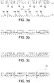
- Figure 3 shows an example of embodiment of the manufacturing method of the sensor described herein. The method is based on the formation of the microreservoir and the microchannel and its bonding on the ISFET using planar technology processes, such as those used for the manufacturing of microfluidic systems.
- Figure 3A shows a first wafer (16) where previously and equally spaced it has integrated ISFETs, (20) and connection pads (14) and a second wafer (17) with microreservoirs (18) and microchannels (19) previously made in its lower surface.
- This second wafer (17) is of a material which means it can be bonded to the first wafer (16).
- Both wafers (16,17) are aligned so that a microchannel (19) and a microreservoir (18) corresponds to each ISFET (20).
- the phase wherein the bonding between both wafers (16,17) is performed is shown in figure 3B .
- the bonding is preferably of chemical type, i.e. by means of the functionalization of the surfaces with molecules which react forming covalent bonds, but other bonding techniques, provided that the geometry of the microchannels (19) is not distorted.
- Many combinations of materials are known in the state of the art which may be functionalized and chemically bonded.
- the first wafer (16) has the surface of silicon oxide or oxynitride and the second wafer (17) is of polydimethylsiloxane (PDMS), both functionalized by means of an oxygen plasma.
- PDMS polydimethylsiloxane
- the second wafer (17) is of easy manufacturing with micro-manufacturing techniques used for the implementation of microfluidic systems. It is provided that it has the structure already formed by moulding or some other technique.
- the ISFETs (20) are manufactured with a technology that allows them to be insulated from the substrate (8). Said technique is based on the use of SOI wafers and the definition of insulation trenches around the ISFET. In this way it facilitates the encapsulation since it is no longer necessary to protect the chip edges. This allows encapsulating chips with a more reduced area, since the distance of the ISFET gate to the chip edges is no longer critical as there is no danger of the gate being accidentally covered when the encapsulating polymer is applied.
- Figure 4 shows another alternative manufacturing technique of the REFET wherein a REFET is obtained by layer addition starting from a chip where an ISFET is integrated.
- Figure 4a shows an ISFET on a chip (22) wherein said ISFET comprises a source pad (23) connected to the source (27) of the transistor, a drain pad (25) connected to the drain (28) of the transistor and a substrate pad (24) (all of them form the connection pads (14) of the ISFET) and a gate (26).
- a first layer (29) of polymer is deposited by bonding or a pre-polymer is deposited by centrifugation and is then heat cured, as shown in figure 4b .
- This layer of polymer (29) is structured ( figure 4c ) by lithography creating the microchannel (30) and the microreservoir (31) and leaving the connection pads (23,24,25) free of polymer. Subsequently, and as shown in figure 4d , a second layer (32) of polymer is bonded by lamination on the first layer (29) of polymer. Again, this second layer (32) of polymer is structured by photolithography increasing the volume of the microreservoir (31) and closing the microchannel (30) ( figure 4e ) but leaving free the outlet orifice (33) of the microchannel (30).
- a third layer (34) of polymer is bonded and it is structured by lithography ( figures 4f and 4g ) thus the microreservoir (31) remains closed and only the outlet orifice (33) of the microchannel (30) remains open.
- the three layers of polymer (29,32,34), which may be SU8, define the microreservoir (31) and the microchannel (30) which in turn is connected to the exterior through its outlet orifice (33). This outlet orifice (33) allows the filling to wafer level of the microchannel (30) and the microreservoir (31) with hydrogel or with any reference solution.
- the structure of an ISFET is similar to that of a MOS transistor (diffusion of drain and source in a doped semiconductor substrate) with the difference that it does not have a gate electrode and the gate dielectric is exposed. So that the ISFET and REFET devices function correctly they must have the gate dielectric in contact with the solution, the ISFET gate dielectric with the solution that one wants to measure and the REFET gate dielectric with the reference solution, but they must have the drain, the source and the substrate insulated from the respective solutions. To guarantee this, a layer of insulating material is deposited on the chip surface during its manufacturing (at wafer level), and the chip edges are protected with the encapsulating polymer during the encapsulating process.
- the second option via the se of SOI wafers becomes more suitable for the manufacturing of the ISFET-REFET sensor described herein, since it allows the encapsulation of chips of reduced area, only requiring that the separation is large in one direction (for example, in a rectangular chip the ISFET gate would be situated at one end of the chip and the connection pads to protect with glob-top at the other end of the chip).
- An interesting variant of the REFET is the one where microreservoir and the microchannel are filled with a hydrogel.
- the advantages in this case are of avoiding problems of bubble formation in the microchannel and the microreservoir (which could cause malfunctioning) and the possibility of storing the sensor dry until its use.
- the hydrogel would be soaked in the reference solution and would perform the same function as the internal solution without hydrogel. This material is very hygroscopic, so that it would take a lot longer to dry if the sensor was left outside the solution. In the event of totally drying, it could be easily rehydrated by re-immersing in distilled water or in reference solution without the danger of bubbles forming.
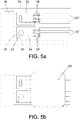
- Figure 5 shows a plan view of an example of embodiment of a pH sensor in accordance with the present invention.
- Figure 5a shows a PCB substrate (35) wherein an ISFET and a REFET such as those described in figure 4 , an electrode (36) and connection tracks (37) have been fixed. Said tracks are connected both to the ISFET and the REFET by the connection pads (23,24,25) by wire bonding (38).
- Figure 5b shows the sensor of figure 5a wherein the encapsulating material (39) has been deposited, which partially covers both the ISFET and the REFET and totally covers the connections thereof with the connection tracks (37).
- Another object of the invention is also an ion measurement method using an ISFET/REFET sensor described.
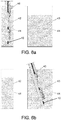
- the sensor (40) is introduced in a conditioning receptacle (41) filled with a reference solution (42) ( Figure 6a ).
- This reference solution (42) also serves as calibration solution as its ion concentration is known.
- the sensor (40) is removed from the conditioning receptacle (41), it is rinsed and immersed in the solution to measure (43) situated within a measurement receptacle (44), keeping the microreservoir (6) of the REFET filled with the reference solution (42) ( figure 6b ).
- the sensor (40) is cleaned and is re-inserted in the conditioning receptacle (41) so that the microreservoir (6) solution is balanced with a receptacle solution and returns to its original ion concentration.
- the sensor (40) would function correctly whenever the time of use is less than the time wherein the sensor (40) is immersed in the reference solution (42) within the conditioning receptacle.
- the present invention is novel in that the sensor (40) is maintained in the conditioning receptacle (41) between one measurement and the next, which means that the sensor does not have a limited lifetime due to contamination of the reference solution or of diffusion of its components towards the exterior.
- the conditioning receptacle (41) is filled with the reference solution (42), whose ion concentration is fixed (for example a buffered solution to maintain the constant pH in the event that the ISFET is selective to the pH and the REFET is constructed with a pH-selective ISFET), the sensor can be calibrated before its removal in the same way transparent to the user.
- the reference solution (42) for example a buffered solution to maintain the constant pH in the event that the ISFET is selective to the pH and the REFET is constructed with a pH-selective ISFET
- the ion sensor object of the present invention is that of integrating the sensor in a self-diagnostic medical device by the measurement of, for example, ions in urine, which may be of interest for controlling diseases such as lithiasis and osteoporosis.
- Another possible application would be the measurement of vaginal pH for birth control, where the measurement made by the sensor was transmitted to a mobile device (for this the sensor object of the present invention must have a communication interface with the mobile device).
- Another possible application for the sensor would be the monitoring of ions in cell cultures. Introducing the sensor within the culture medium, it would be possible to continuously control the state of the cells without the need to open the receptacle lid. In this case the measurement it could be transmitted to a wireless communication system integrated in the sensor.
Landscapes
- Health & Medical Sciences (AREA)
- Life Sciences & Earth Sciences (AREA)
- Chemical & Material Sciences (AREA)
- Engineering & Computer Science (AREA)
- Microelectronics & Electronic Packaging (AREA)
- Physics & Mathematics (AREA)
- General Physics & Mathematics (AREA)
- Analytical Chemistry (AREA)
- Electrochemistry (AREA)
- Chemical Kinetics & Catalysis (AREA)
- Molecular Biology (AREA)
- Biochemistry (AREA)
- General Health & Medical Sciences (AREA)
- Immunology (AREA)
- Pathology (AREA)
- Computer Hardware Design (AREA)
- Condensed Matter Physics & Semiconductors (AREA)
- Power Engineering (AREA)
- Manufacturing & Machinery (AREA)
- Investigating Or Analyzing Materials By The Use Of Electric Means (AREA)
Applications Claiming Priority (2)
| Application Number | Priority Date | Filing Date | Title |
|---|---|---|---|
| ES201430180A ES2542927R1 (es) | 2014-02-11 | 2014-02-11 | Sensor de iones basado en medida diferencial, método de fabricación y método de medida |
| PCT/ES2015/070063 WO2015121516A1 (es) | 2014-02-11 | 2015-01-29 | Sensor de iones basado en medida diferencial y método de fabricación |
Publications (2)
| Publication Number | Publication Date |
|---|---|
| EP3106865A1 EP3106865A1 (en) | 2016-12-21 |
| EP3106865B1 true EP3106865B1 (en) | 2020-06-10 |
Family
ID=52633296
Family Applications (1)
| Application Number | Title | Priority Date | Filing Date |
|---|---|---|---|
| EP15708848.5A Active EP3106865B1 (en) | 2014-02-11 | 2015-01-29 | Ion sensor based on differential measurement, and production method |
Country Status (9)
| Country | Link |
|---|---|
| US (3) | US10067085B2 (enExample) |
| EP (1) | EP3106865B1 (enExample) |
| JP (1) | JP2017505443A (enExample) |
| KR (1) | KR20160119096A (enExample) |
| CN (1) | CN106104265A (enExample) |
| CA (1) | CA2938155A1 (enExample) |
| ES (2) | ES2542927R1 (enExample) |
| MX (1) | MX2016010017A (enExample) |
| WO (1) | WO2015121516A1 (enExample) |
Families Citing this family (11)
| Publication number | Priority date | Publication date | Assignee | Title |
|---|---|---|---|---|
| ES2542927R1 (es) | 2014-02-11 | 2015-09-09 | Consejo Superior De Investigaciones Científicas (Csic) | Sensor de iones basado en medida diferencial, método de fabricación y método de medida |
| ES2597129B1 (es) | 2015-07-13 | 2017-11-08 | Consejo Superior De Investigaciones Científicas (Csic) | Sensor de iones de medida diferencial |
| WO2018210803A1 (en) * | 2017-05-15 | 2018-11-22 | Analog Devices Global Unlimited Company | Integrated ion sensing apparatus and methods |
| WO2019093907A1 (en) | 2017-11-07 | 2019-05-16 | Lic Automation Limited | System and method for analysis of a fluid |
| JP7173731B2 (ja) * | 2017-12-15 | 2022-11-16 | 株式会社 堀場アドバンスドテクノ | 電磁気センサ |
| CN108565262A (zh) * | 2018-04-17 | 2018-09-21 | 重庆第二师范学院 | 一种用于生化分析的阵列式传感器集成芯片及其制备方法 |
| US20200316002A1 (en) * | 2019-04-03 | 2020-10-08 | Devicare SL | Prevention of urinary tract device encrustation |
| WO2021146105A1 (en) * | 2020-01-13 | 2021-07-22 | Beckman Coulter, Inc. | Solid state ion selective electrodes |
| JP7611795B2 (ja) * | 2021-09-29 | 2025-01-10 | ラピスセミコンダクタ株式会社 | 測定装置、測定方法、イオン感応半導体デバイス |
| SE545362C2 (en) * | 2021-12-22 | 2023-07-18 | Senseair Ab | Capped semiconductor based sensor and method for its fabrication |
| CN119470598B (zh) * | 2025-01-14 | 2025-04-22 | 南京大学 | 一种半导体场效应晶体管液体传感器及其制造方法 |
Family Cites Families (24)
| Publication number | Priority date | Publication date | Assignee | Title |
|---|---|---|---|---|
| GB2096825A (en) * | 1981-04-09 | 1982-10-20 | Sibbald Alastair | Chemical sensitive semiconductor field effect transducer |
| EP0155725A1 (en) | 1984-02-27 | 1985-09-25 | Sentron v.o.f. | Ion concentration measurement system that employs measuring and reference field effect transistor electrodes sensitive to the same ion |
| JPS63128253A (ja) * | 1986-11-19 | 1988-05-31 | Seitai Kinou Riyou Kagakuhin Shinseizou Gijutsu Kenkyu Kumiai | 半導体化学センサ |
| US4874499A (en) * | 1988-05-23 | 1989-10-17 | Massachusetts Institute Of Technology | Electrochemical microsensors and method of making such sensors |
| US5250168A (en) | 1990-07-03 | 1993-10-05 | Hitachi, Ltd. | Integrated ion sensor |
| JPH0580026A (ja) * | 1991-09-24 | 1993-03-30 | Fuji Electric Co Ltd | 半導体イオンセンサ |
| TW533593B (en) * | 2002-05-20 | 2003-05-21 | Univ Nat Yunlin Sci & Tech | Method of manufacturing amorphous hydrocarbon pH ion sensitive field effect transistor and method and device of measuring temperature parameter, drift and hysteresis thereof |
| GB2416210B (en) * | 2004-07-13 | 2008-02-20 | Christofer Toumazou | Ion sensitive field effect transistors |
| JP4731544B2 (ja) * | 2007-12-17 | 2011-07-27 | 株式会社日立製作所 | 生体分子検出装置及びそれを用いた生体分子検出方法 |
| WO2009119319A1 (ja) * | 2008-03-27 | 2009-10-01 | 株式会社堀場製作所 | イオンセンサ |
| WO2010017192A1 (en) * | 2008-08-05 | 2010-02-11 | Ph Diagnostics Inc. | Apparatus, method and system for determining a physiological condition within a mammal |
| US9518953B2 (en) * | 2011-09-07 | 2016-12-13 | Technion Research And Development Foundation Ltd. | Ion sensitive detector |
| EP2570803B1 (en) * | 2011-09-16 | 2018-03-21 | Nxp B.V. | pH sensor and manufacturing method |
| US20130158378A1 (en) * | 2011-09-22 | 2013-06-20 | The Ohio State University | Ionic barrier for floating gate in vivo biosensors |
| US20130084214A1 (en) * | 2011-09-30 | 2013-04-04 | Frederick Quincy Johnson | Ion-Selective Ion Concentration Meter |
| US9304103B2 (en) * | 2011-09-30 | 2016-04-05 | Sentient Technologies, Inc. | Self-calibrating ion meter |
| US9459234B2 (en) * | 2011-10-31 | 2016-10-04 | Taiwan Semiconductor Manufacturing Company, Ltd., (“TSMC”) | CMOS compatible BioFET |
| US9689835B2 (en) * | 2011-10-31 | 2017-06-27 | Taiwan Semiconductor Manufacturing Company, Ltd. | Amplified dual-gate bio field effect transistor |
| US8963216B2 (en) * | 2013-03-13 | 2015-02-24 | Life Technologies Corporation | Chemical sensor with sidewall spacer sensor surface |
| EP2986966B1 (en) * | 2013-04-18 | 2023-06-07 | Solenis Technologies Cayman, L.P. | Device and method for detecting and analyzing deposits |
| KR101540254B1 (ko) * | 2013-06-24 | 2015-07-30 | 경북대학교 산학협력단 | 당을 감지하는 화학감각수용체를 발현하는 세포를 이용한 바이오 센서 및 이를 포함하는 알츠하이머 진단 기기 |
| US9978689B2 (en) * | 2013-12-18 | 2018-05-22 | Nxp Usa, Inc. | Ion sensitive field effect transistors with protection diodes and methods of their fabrication |
| ES2542927R1 (es) * | 2014-02-11 | 2015-09-09 | Consejo Superior De Investigaciones Científicas (Csic) | Sensor de iones basado en medida diferencial, método de fabricación y método de medida |
| US9733210B2 (en) * | 2014-12-31 | 2017-08-15 | International Business Machines Corporation | Nanofluid sensor with real-time spatial sensing |
-
2014
- 2014-02-11 ES ES201430180A patent/ES2542927R1/es active Granted
-
2015
- 2015-01-29 CN CN201580007758.0A patent/CN106104265A/zh active Pending
- 2015-01-29 ES ES15708848T patent/ES2818111T3/es active Active
- 2015-01-29 KR KR1020167021498A patent/KR20160119096A/ko not_active Withdrawn
- 2015-01-29 WO PCT/ES2015/070063 patent/WO2015121516A1/es not_active Ceased
- 2015-01-29 MX MX2016010017A patent/MX2016010017A/es unknown
- 2015-01-29 CA CA2938155A patent/CA2938155A1/en not_active Abandoned
- 2015-01-29 EP EP15708848.5A patent/EP3106865B1/en active Active
- 2015-01-29 US US15/113,381 patent/US10067085B2/en active Active
- 2015-01-29 JP JP2016550810A patent/JP2017505443A/ja active Pending
-
2018
- 2018-06-28 US US16/021,926 patent/US10436743B2/en active Active
-
2019
- 2019-08-02 US US16/530,574 patent/US11029278B2/en active Active
Non-Patent Citations (1)
| Title |
|---|
| ERRACHID A ET AL: "A simple REFET for pH detection in differential mode", SENSORS AND ACTUATORS B: CHEMICAL: INTERNATIONAL JOURNAL DEVOTED TO RESEARCH AND DEVELOPMENT OF PHYSICAL AND CHEMICAL TRANSDU, ELSEVIER BV, NL, vol. 60, no. 1, 2 November 1999 (1999-11-02), pages 43 - 48, XP004244599, ISSN: 0925-4005, DOI: 10.1016/S0925-4005(99)00242-7 * |
Also Published As
| Publication number | Publication date |
|---|---|
| US20200025710A1 (en) | 2020-01-23 |
| CN106104265A (zh) | 2016-11-09 |
| ES2818111T3 (es) | 2021-04-09 |
| US10067085B2 (en) | 2018-09-04 |
| US10436743B2 (en) | 2019-10-08 |
| CA2938155A1 (en) | 2015-08-20 |
| ES2542927A2 (es) | 2015-08-12 |
| KR20160119096A (ko) | 2016-10-12 |
| US20190017958A1 (en) | 2019-01-17 |
| EP3106865A1 (en) | 2016-12-21 |
| US20170010237A1 (en) | 2017-01-12 |
| WO2015121516A1 (es) | 2015-08-20 |
| MX2016010017A (es) | 2016-10-07 |
| ES2542927R1 (es) | 2015-09-09 |
| JP2017505443A (ja) | 2017-02-16 |
| US11029278B2 (en) | 2021-06-08 |
Similar Documents
| Publication | Publication Date | Title |
|---|---|---|
| US11029278B2 (en) | Ion sensor based on differential measurement, and production method | |
| US4874499A (en) | Electrochemical microsensors and method of making such sensors | |
| US4739380A (en) | Integrated ambient sensing devices and methods of manufacture | |
| CN102132153B (zh) | 减小电子设备中的电容性充电 | |
| Bergveld | Thirty years of ISFETOLOGY: What happened in the past 30 years and what may happen in the next 30 years | |
| EP2570803B1 (en) | pH sensor and manufacturing method | |
| US10895548B2 (en) | Reference electrode with a pore membrane | |
| US9791398B2 (en) | Measurement device with sensor array | |
| US9964509B2 (en) | Drift compensated ion sensor | |
| JP4456303B2 (ja) | pHセンサ | |
| CN111108374A (zh) | PH传感器和用于pH传感器的校准方法 | |
| US5384031A (en) | Reference electrode | |
| CN106959330B (zh) | 集成离子感测装置和方法 | |
| US9128035B2 (en) | Sensor for registering an analyte concentration | |
| Baldi Coll et al. | Ion sensor based on differential measurement, and production method | |
| ES2542927B1 (es) | Sensor de iones basado en medida diferencial, método de fabricación y método de medida | |
| Prathap | Silicon Ion Sensitive Field Effect Transistor Circuitry Architectures for Improved On-Chip pH Sensing | |
| KR0168828B1 (ko) | 반도체형 용존 가스 센서 | |
| JPS62250353A (ja) | 半導体化学センサ | |
| Wiley et al. | Measurement of pH | |
| AU2016200041A1 (en) | Measurement device with sensor array |
Legal Events
| Date | Code | Title | Description |
|---|---|---|---|
| PUAI | Public reference made under article 153(3) epc to a published international application that has entered the european phase |
Free format text: ORIGINAL CODE: 0009012 |
|
| STAA | Information on the status of an ep patent application or granted ep patent |
Free format text: STATUS: REQUEST FOR EXAMINATION WAS MADE |
|
| 17P | Request for examination filed |
Effective date: 20160906 |
|
| AK | Designated contracting states |
Kind code of ref document: A1 Designated state(s): AL AT BE BG CH CY CZ DE DK EE ES FI FR GB GR HR HU IE IS IT LI LT LU LV MC MK MT NL NO PL PT RO RS SE SI SK SM TR |
|
| AX | Request for extension of the european patent |
Extension state: BA ME |
|
| DAX | Request for extension of the european patent (deleted) | ||
| RIC1 | Information provided on ipc code assigned before grant |
Ipc: G01N 27/414 20060101AFI20180508BHEP Ipc: H01L 27/12 20060101ALI20180508BHEP Ipc: H01L 21/78 20060101ALI20180508BHEP Ipc: H01L 23/31 20060101ALI20180508BHEP |
|
| GRAP | Despatch of communication of intention to grant a patent |
Free format text: ORIGINAL CODE: EPIDOSNIGR1 |
|
| STAA | Information on the status of an ep patent application or granted ep patent |
Free format text: STATUS: GRANT OF PATENT IS INTENDED |
|
| INTG | Intention to grant announced |
Effective date: 20180706 |
|
| GRAJ | Information related to disapproval of communication of intention to grant by the applicant or resumption of examination proceedings by the epo deleted |
Free format text: ORIGINAL CODE: EPIDOSDIGR1 |
|
| STAA | Information on the status of an ep patent application or granted ep patent |
Free format text: STATUS: REQUEST FOR EXAMINATION WAS MADE |
|
| GRAP | Despatch of communication of intention to grant a patent |
Free format text: ORIGINAL CODE: EPIDOSNIGR1 |
|
| STAA | Information on the status of an ep patent application or granted ep patent |
Free format text: STATUS: GRANT OF PATENT IS INTENDED |
|
| INTC | Intention to grant announced (deleted) | ||
| INTG | Intention to grant announced |
Effective date: 20181130 |
|
| GRAJ | Information related to disapproval of communication of intention to grant by the applicant or resumption of examination proceedings by the epo deleted |
Free format text: ORIGINAL CODE: EPIDOSDIGR1 |
|
| STAA | Information on the status of an ep patent application or granted ep patent |
Free format text: STATUS: REQUEST FOR EXAMINATION WAS MADE |
|
| INTC | Intention to grant announced (deleted) | ||
| GRAP | Despatch of communication of intention to grant a patent |
Free format text: ORIGINAL CODE: EPIDOSNIGR1 |
|
| STAA | Information on the status of an ep patent application or granted ep patent |
Free format text: STATUS: GRANT OF PATENT IS INTENDED |
|
| INTG | Intention to grant announced |
Effective date: 20190523 |
|
| GRAJ | Information related to disapproval of communication of intention to grant by the applicant or resumption of examination proceedings by the epo deleted |
Free format text: ORIGINAL CODE: EPIDOSDIGR1 |
|
| STAA | Information on the status of an ep patent application or granted ep patent |
Free format text: STATUS: REQUEST FOR EXAMINATION WAS MADE |
|
| GRAP | Despatch of communication of intention to grant a patent |
Free format text: ORIGINAL CODE: EPIDOSNIGR1 |
|
| STAA | Information on the status of an ep patent application or granted ep patent |
Free format text: STATUS: GRANT OF PATENT IS INTENDED |
|
| INTC | Intention to grant announced (deleted) | ||
| INTG | Intention to grant announced |
Effective date: 20191111 |
|
| GRAS | Grant fee paid |
Free format text: ORIGINAL CODE: EPIDOSNIGR3 |
|
| GRAA | (expected) grant |
Free format text: ORIGINAL CODE: 0009210 |
|
| STAA | Information on the status of an ep patent application or granted ep patent |
Free format text: STATUS: THE PATENT HAS BEEN GRANTED |
|
| AK | Designated contracting states |
Kind code of ref document: B1 Designated state(s): AL AT BE BG CH CY CZ DE DK EE ES FI FR GB GR HR HU IE IS IT LI LT LU LV MC MK MT NL NO PL PT RO RS SE SI SK SM TR |
|
| REG | Reference to a national code |
Ref country code: GB Ref legal event code: FG4D |
|
| REG | Reference to a national code |
Ref country code: AT Ref legal event code: REF Ref document number: 1279590 Country of ref document: AT Kind code of ref document: T Effective date: 20200615 Ref country code: CH Ref legal event code: EP |
|
| REG | Reference to a national code |
Ref country code: DE Ref legal event code: R096 Ref document number: 602015054034 Country of ref document: DE |
|
| REG | Reference to a national code |
Ref country code: IE Ref legal event code: FG4D |
|
| REG | Reference to a national code |
Ref country code: LT Ref legal event code: MG4D |
|
| PG25 | Lapsed in a contracting state [announced via postgrant information from national office to epo] |
Ref country code: LT Free format text: LAPSE BECAUSE OF FAILURE TO SUBMIT A TRANSLATION OF THE DESCRIPTION OR TO PAY THE FEE WITHIN THE PRESCRIBED TIME-LIMIT Effective date: 20200610 Ref country code: SE Free format text: LAPSE BECAUSE OF FAILURE TO SUBMIT A TRANSLATION OF THE DESCRIPTION OR TO PAY THE FEE WITHIN THE PRESCRIBED TIME-LIMIT Effective date: 20200610 Ref country code: FI Free format text: LAPSE BECAUSE OF FAILURE TO SUBMIT A TRANSLATION OF THE DESCRIPTION OR TO PAY THE FEE WITHIN THE PRESCRIBED TIME-LIMIT Effective date: 20200610 Ref country code: GR Free format text: LAPSE BECAUSE OF FAILURE TO SUBMIT A TRANSLATION OF THE DESCRIPTION OR TO PAY THE FEE WITHIN THE PRESCRIBED TIME-LIMIT Effective date: 20200911 Ref country code: NO Free format text: LAPSE BECAUSE OF FAILURE TO SUBMIT A TRANSLATION OF THE DESCRIPTION OR TO PAY THE FEE WITHIN THE PRESCRIBED TIME-LIMIT Effective date: 20200910 |
|
| REG | Reference to a national code |
Ref country code: NL Ref legal event code: MP Effective date: 20200610 |
|
| PG25 | Lapsed in a contracting state [announced via postgrant information from national office to epo] |
Ref country code: LV Free format text: LAPSE BECAUSE OF FAILURE TO SUBMIT A TRANSLATION OF THE DESCRIPTION OR TO PAY THE FEE WITHIN THE PRESCRIBED TIME-LIMIT Effective date: 20200610 Ref country code: RS Free format text: LAPSE BECAUSE OF FAILURE TO SUBMIT A TRANSLATION OF THE DESCRIPTION OR TO PAY THE FEE WITHIN THE PRESCRIBED TIME-LIMIT Effective date: 20200610 Ref country code: HR Free format text: LAPSE BECAUSE OF FAILURE TO SUBMIT A TRANSLATION OF THE DESCRIPTION OR TO PAY THE FEE WITHIN THE PRESCRIBED TIME-LIMIT Effective date: 20200610 Ref country code: BG Free format text: LAPSE BECAUSE OF FAILURE TO SUBMIT A TRANSLATION OF THE DESCRIPTION OR TO PAY THE FEE WITHIN THE PRESCRIBED TIME-LIMIT Effective date: 20200910 |
|
| REG | Reference to a national code |
Ref country code: AT Ref legal event code: MK05 Ref document number: 1279590 Country of ref document: AT Kind code of ref document: T Effective date: 20200610 |
|
| PG25 | Lapsed in a contracting state [announced via postgrant information from national office to epo] |
Ref country code: AL Free format text: LAPSE BECAUSE OF FAILURE TO SUBMIT A TRANSLATION OF THE DESCRIPTION OR TO PAY THE FEE WITHIN THE PRESCRIBED TIME-LIMIT Effective date: 20200610 Ref country code: NL Free format text: LAPSE BECAUSE OF FAILURE TO SUBMIT A TRANSLATION OF THE DESCRIPTION OR TO PAY THE FEE WITHIN THE PRESCRIBED TIME-LIMIT Effective date: 20200610 |
|
| PG25 | Lapsed in a contracting state [announced via postgrant information from national office to epo] |
Ref country code: CZ Free format text: LAPSE BECAUSE OF FAILURE TO SUBMIT A TRANSLATION OF THE DESCRIPTION OR TO PAY THE FEE WITHIN THE PRESCRIBED TIME-LIMIT Effective date: 20200610 Ref country code: RO Free format text: LAPSE BECAUSE OF FAILURE TO SUBMIT A TRANSLATION OF THE DESCRIPTION OR TO PAY THE FEE WITHIN THE PRESCRIBED TIME-LIMIT Effective date: 20200610 Ref country code: IT Free format text: LAPSE BECAUSE OF FAILURE TO SUBMIT A TRANSLATION OF THE DESCRIPTION OR TO PAY THE FEE WITHIN THE PRESCRIBED TIME-LIMIT Effective date: 20200610 Ref country code: SM Free format text: LAPSE BECAUSE OF FAILURE TO SUBMIT A TRANSLATION OF THE DESCRIPTION OR TO PAY THE FEE WITHIN THE PRESCRIBED TIME-LIMIT Effective date: 20200610 Ref country code: EE Free format text: LAPSE BECAUSE OF FAILURE TO SUBMIT A TRANSLATION OF THE DESCRIPTION OR TO PAY THE FEE WITHIN THE PRESCRIBED TIME-LIMIT Effective date: 20200610 Ref country code: AT Free format text: LAPSE BECAUSE OF FAILURE TO SUBMIT A TRANSLATION OF THE DESCRIPTION OR TO PAY THE FEE WITHIN THE PRESCRIBED TIME-LIMIT Effective date: 20200610 Ref country code: PT Free format text: LAPSE BECAUSE OF FAILURE TO SUBMIT A TRANSLATION OF THE DESCRIPTION OR TO PAY THE FEE WITHIN THE PRESCRIBED TIME-LIMIT Effective date: 20201012 |
|
| PG25 | Lapsed in a contracting state [announced via postgrant information from national office to epo] |
Ref country code: IS Free format text: LAPSE BECAUSE OF FAILURE TO SUBMIT A TRANSLATION OF THE DESCRIPTION OR TO PAY THE FEE WITHIN THE PRESCRIBED TIME-LIMIT Effective date: 20201010 Ref country code: SK Free format text: LAPSE BECAUSE OF FAILURE TO SUBMIT A TRANSLATION OF THE DESCRIPTION OR TO PAY THE FEE WITHIN THE PRESCRIBED TIME-LIMIT Effective date: 20200610 Ref country code: PL Free format text: LAPSE BECAUSE OF FAILURE TO SUBMIT A TRANSLATION OF THE DESCRIPTION OR TO PAY THE FEE WITHIN THE PRESCRIBED TIME-LIMIT Effective date: 20200610 |
|
| REG | Reference to a national code |
Ref country code: DE Ref legal event code: R097 Ref document number: 602015054034 Country of ref document: DE |
|
| REG | Reference to a national code |
Ref country code: ES Ref legal event code: FG2A Ref document number: 2818111 Country of ref document: ES Kind code of ref document: T3 Effective date: 20210409 |
|
| PLBE | No opposition filed within time limit |
Free format text: ORIGINAL CODE: 0009261 |
|
| STAA | Information on the status of an ep patent application or granted ep patent |
Free format text: STATUS: NO OPPOSITION FILED WITHIN TIME LIMIT |
|
| PG25 | Lapsed in a contracting state [announced via postgrant information from national office to epo] |
Ref country code: DK Free format text: LAPSE BECAUSE OF FAILURE TO SUBMIT A TRANSLATION OF THE DESCRIPTION OR TO PAY THE FEE WITHIN THE PRESCRIBED TIME-LIMIT Effective date: 20200610 |
|
| 26N | No opposition filed |
Effective date: 20210311 |
|
| PG25 | Lapsed in a contracting state [announced via postgrant information from national office to epo] |
Ref country code: SI Free format text: LAPSE BECAUSE OF FAILURE TO SUBMIT A TRANSLATION OF THE DESCRIPTION OR TO PAY THE FEE WITHIN THE PRESCRIBED TIME-LIMIT Effective date: 20200610 |
|
| PG25 | Lapsed in a contracting state [announced via postgrant information from national office to epo] |
Ref country code: MC Free format text: LAPSE BECAUSE OF FAILURE TO SUBMIT A TRANSLATION OF THE DESCRIPTION OR TO PAY THE FEE WITHIN THE PRESCRIBED TIME-LIMIT Effective date: 20200610 |
|
| REG | Reference to a national code |
Ref country code: CH Ref legal event code: PL |
|
| PG25 | Lapsed in a contracting state [announced via postgrant information from national office to epo] |
Ref country code: LU Free format text: LAPSE BECAUSE OF NON-PAYMENT OF DUE FEES Effective date: 20210129 |
|
| REG | Reference to a national code |
Ref country code: BE Ref legal event code: MM Effective date: 20210131 |
|
| PG25 | Lapsed in a contracting state [announced via postgrant information from national office to epo] |
Ref country code: CH Free format text: LAPSE BECAUSE OF NON-PAYMENT OF DUE FEES Effective date: 20210131 Ref country code: LI Free format text: LAPSE BECAUSE OF NON-PAYMENT OF DUE FEES Effective date: 20210131 |
|
| PG25 | Lapsed in a contracting state [announced via postgrant information from national office to epo] |
Ref country code: IE Free format text: LAPSE BECAUSE OF NON-PAYMENT OF DUE FEES Effective date: 20210129 |
|
| PG25 | Lapsed in a contracting state [announced via postgrant information from national office to epo] |
Ref country code: BE Free format text: LAPSE BECAUSE OF NON-PAYMENT OF DUE FEES Effective date: 20210131 |
|
| PG25 | Lapsed in a contracting state [announced via postgrant information from national office to epo] |
Ref country code: HU Free format text: LAPSE BECAUSE OF FAILURE TO SUBMIT A TRANSLATION OF THE DESCRIPTION OR TO PAY THE FEE WITHIN THE PRESCRIBED TIME-LIMIT; INVALID AB INITIO Effective date: 20150129 |
|
| PG25 | Lapsed in a contracting state [announced via postgrant information from national office to epo] |
Ref country code: CY Free format text: LAPSE BECAUSE OF FAILURE TO SUBMIT A TRANSLATION OF THE DESCRIPTION OR TO PAY THE FEE WITHIN THE PRESCRIBED TIME-LIMIT Effective date: 20200610 |
|
| P01 | Opt-out of the competence of the unified patent court (upc) registered |
Effective date: 20230623 |
|
| PG25 | Lapsed in a contracting state [announced via postgrant information from national office to epo] |
Ref country code: MK Free format text: LAPSE BECAUSE OF FAILURE TO SUBMIT A TRANSLATION OF THE DESCRIPTION OR TO PAY THE FEE WITHIN THE PRESCRIBED TIME-LIMIT Effective date: 20200610 |
|
| PG25 | Lapsed in a contracting state [announced via postgrant information from national office to epo] |
Ref country code: MT Free format text: LAPSE BECAUSE OF FAILURE TO SUBMIT A TRANSLATION OF THE DESCRIPTION OR TO PAY THE FEE WITHIN THE PRESCRIBED TIME-LIMIT Effective date: 20200610 |
|
| PGFP | Annual fee paid to national office [announced via postgrant information from national office to epo] |
Ref country code: DE Payment date: 20250129 Year of fee payment: 11 |
|
| PGFP | Annual fee paid to national office [announced via postgrant information from national office to epo] |
Ref country code: ES Payment date: 20250203 Year of fee payment: 11 |
|
| PGFP | Annual fee paid to national office [announced via postgrant information from national office to epo] |
Ref country code: FR Payment date: 20250127 Year of fee payment: 11 |
|
| PGFP | Annual fee paid to national office [announced via postgrant information from national office to epo] |
Ref country code: GB Payment date: 20250127 Year of fee payment: 11 |