EP3101766B1 - Ladevorrichtung für elektronische vorrichtung und leistungsadapter für elektronische vorrichtung - Google Patents
Ladevorrichtung für elektronische vorrichtung und leistungsadapter für elektronische vorrichtung Download PDFInfo
- Publication number
- EP3101766B1 EP3101766B1 EP14880925.4A EP14880925A EP3101766B1 EP 3101766 B1 EP3101766 B1 EP 3101766B1 EP 14880925 A EP14880925 A EP 14880925A EP 3101766 B1 EP3101766 B1 EP 3101766B1
- Authority
- EP
- European Patent Office
- Prior art keywords
- voltage
- power adapter
- output
- terminal
- quick charge
- Prior art date
- Legal status (The legal status is an assumption and is not a legal conclusion. Google has not performed a legal analysis and makes no representation as to the accuracy of the status listed.)
- Active
Links
- 238000001514 detection method Methods 0.000 claims description 82
- 238000002955 isolation Methods 0.000 claims description 34
- 239000003990 capacitor Substances 0.000 description 47
- 230000000087 stabilizing effect Effects 0.000 description 11
- 238000000034 method Methods 0.000 description 9
- 238000010586 diagram Methods 0.000 description 3
- 230000002159 abnormal effect Effects 0.000 description 2
- 101100219315 Arabidopsis thaliana CYP83A1 gene Proteins 0.000 description 1
- 101000806846 Homo sapiens DNA-(apurinic or apyrimidinic site) endonuclease Proteins 0.000 description 1
- 101000835083 Homo sapiens Tissue factor pathway inhibitor 2 Proteins 0.000 description 1
- 101100269674 Mus musculus Alyref2 gene Proteins 0.000 description 1
- 101100489713 Saccharomyces cerevisiae (strain ATCC 204508 / S288c) GND1 gene Proteins 0.000 description 1
- 101100489717 Saccharomyces cerevisiae (strain ATCC 204508 / S288c) GND2 gene Proteins 0.000 description 1
- 101100140580 Saccharomyces cerevisiae (strain ATCC 204508 / S288c) REF2 gene Proteins 0.000 description 1
- 102100026134 Tissue factor pathway inhibitor 2 Human genes 0.000 description 1
- 238000006243 chemical reaction Methods 0.000 description 1
- 230000001419 dependent effect Effects 0.000 description 1
- 238000001914 filtration Methods 0.000 description 1
- 238000004904 shortening Methods 0.000 description 1
Images

Classifications
-
- H—ELECTRICITY
- H02—GENERATION; CONVERSION OR DISTRIBUTION OF ELECTRIC POWER
- H02J—CIRCUIT ARRANGEMENTS OR SYSTEMS FOR SUPPLYING OR DISTRIBUTING ELECTRIC POWER; SYSTEMS FOR STORING ELECTRIC ENERGY
- H02J7/00—Circuit arrangements for charging or depolarising batteries or for supplying loads from batteries
- H02J7/02—Circuit arrangements for charging or depolarising batteries or for supplying loads from batteries for charging batteries from ac mains by converters
- H02J7/04—Regulation of charging current or voltage
-
- H—ELECTRICITY
- H02—GENERATION; CONVERSION OR DISTRIBUTION OF ELECTRIC POWER
- H02J—CIRCUIT ARRANGEMENTS OR SYSTEMS FOR SUPPLYING OR DISTRIBUTING ELECTRIC POWER; SYSTEMS FOR STORING ELECTRIC ENERGY
- H02J7/00—Circuit arrangements for charging or depolarising batteries or for supplying loads from batteries
- H02J7/00032—Circuit arrangements for charging or depolarising batteries or for supplying loads from batteries characterised by data exchange
- H02J7/00036—Charger exchanging data with battery
-
- H—ELECTRICITY
- H02—GENERATION; CONVERSION OR DISTRIBUTION OF ELECTRIC POWER
- H02J—CIRCUIT ARRANGEMENTS OR SYSTEMS FOR SUPPLYING OR DISTRIBUTING ELECTRIC POWER; SYSTEMS FOR STORING ELECTRIC ENERGY
- H02J7/00—Circuit arrangements for charging or depolarising batteries or for supplying loads from batteries
- H02J7/0013—Circuit arrangements for charging or depolarising batteries or for supplying loads from batteries acting upon several batteries simultaneously or sequentially
-
- H—ELECTRICITY
- H02—GENERATION; CONVERSION OR DISTRIBUTION OF ELECTRIC POWER
- H02J—CIRCUIT ARRANGEMENTS OR SYSTEMS FOR SUPPLYING OR DISTRIBUTING ELECTRIC POWER; SYSTEMS FOR STORING ELECTRIC ENERGY
- H02J7/00—Circuit arrangements for charging or depolarising batteries or for supplying loads from batteries
- H02J7/0068—Battery or charger load switching, e.g. concurrent charging and load supply
-
- H—ELECTRICITY
- H02—GENERATION; CONVERSION OR DISTRIBUTION OF ELECTRIC POWER
- H02J—CIRCUIT ARRANGEMENTS OR SYSTEMS FOR SUPPLYING OR DISTRIBUTING ELECTRIC POWER; SYSTEMS FOR STORING ELECTRIC ENERGY
- H02J7/00—Circuit arrangements for charging or depolarising batteries or for supplying loads from batteries
- H02J7/007—Regulation of charging or discharging current or voltage
- H02J7/00712—Regulation of charging or discharging current or voltage the cycle being controlled or terminated in response to electric parameters
- H02J7/007182—Regulation of charging or discharging current or voltage the cycle being controlled or terminated in response to electric parameters in response to battery voltage
- H02J7/007184—Regulation of charging or discharging current or voltage the cycle being controlled or terminated in response to electric parameters in response to battery voltage in response to battery voltage gradient
-
- H—ELECTRICITY
- H02—GENERATION; CONVERSION OR DISTRIBUTION OF ELECTRIC POWER
- H02J—CIRCUIT ARRANGEMENTS OR SYSTEMS FOR SUPPLYING OR DISTRIBUTING ELECTRIC POWER; SYSTEMS FOR STORING ELECTRIC ENERGY
- H02J2207/00—Indexing scheme relating to details of circuit arrangements for charging or depolarising batteries or for supplying loads from batteries
- H02J2207/10—Control circuit supply, e.g. means for supplying power to the control circuit
-
- H—ELECTRICITY
- H02—GENERATION; CONVERSION OR DISTRIBUTION OF ELECTRIC POWER
- H02J—CIRCUIT ARRANGEMENTS OR SYSTEMS FOR SUPPLYING OR DISTRIBUTING ELECTRIC POWER; SYSTEMS FOR STORING ELECTRIC ENERGY
- H02J7/00—Circuit arrangements for charging or depolarising batteries or for supplying loads from batteries
- H02J7/00032—Circuit arrangements for charging or depolarising batteries or for supplying loads from batteries characterised by data exchange
- H02J7/00034—Charger exchanging data with an electronic device, i.e. telephone, whose internal battery is under charge
-
- H—ELECTRICITY
- H02—GENERATION; CONVERSION OR DISTRIBUTION OF ELECTRIC POWER
- H02J—CIRCUIT ARRANGEMENTS OR SYSTEMS FOR SUPPLYING OR DISTRIBUTING ELECTRIC POWER; SYSTEMS FOR STORING ELECTRIC ENERGY
- H02J7/00—Circuit arrangements for charging or depolarising batteries or for supplying loads from batteries
- H02J7/0029—Circuit arrangements for charging or depolarising batteries or for supplying loads from batteries with safety or protection devices or circuits
- H02J7/0034—Circuit arrangements for charging or depolarising batteries or for supplying loads from batteries with safety or protection devices or circuits using reverse polarity correcting or protecting circuits
-
- H—ELECTRICITY
- H02—GENERATION; CONVERSION OR DISTRIBUTION OF ELECTRIC POWER
- H02J—CIRCUIT ARRANGEMENTS OR SYSTEMS FOR SUPPLYING OR DISTRIBUTING ELECTRIC POWER; SYSTEMS FOR STORING ELECTRIC ENERGY
- H02J7/00—Circuit arrangements for charging or depolarising batteries or for supplying loads from batteries
- H02J7/0029—Circuit arrangements for charging or depolarising batteries or for supplying loads from batteries with safety or protection devices or circuits
- H02J7/0036—Circuit arrangements for charging or depolarising batteries or for supplying loads from batteries with safety or protection devices or circuits using connection detecting circuits
-
- H—ELECTRICITY
- H02—GENERATION; CONVERSION OR DISTRIBUTION OF ELECTRIC POWER
- H02J—CIRCUIT ARRANGEMENTS OR SYSTEMS FOR SUPPLYING OR DISTRIBUTING ELECTRIC POWER; SYSTEMS FOR STORING ELECTRIC ENERGY
- H02J7/00—Circuit arrangements for charging or depolarising batteries or for supplying loads from batteries
- H02J7/007—Regulation of charging or discharging current or voltage
- H02J7/00712—Regulation of charging or discharging current or voltage the cycle being controlled or terminated in response to electric parameters
- H02J7/00714—Regulation of charging or discharging current or voltage the cycle being controlled or terminated in response to electric parameters in response to battery charging or discharging current
Definitions
- This disclosure relates to charging technical field, and particularly relates to a power adapter, an electronic device and a charging apparatus for an electronic device.
- a battery in an electronic device is charged through a power adapter of the electronic device.
- a constant-voltage output is usually used by the power adapter for charging the battery.
- it will result in too long charging time by charging the battery with the constant-voltage output, and above mentioned charging way cannot realize quick charging for the battery and thus cannot shorten the charging time.
- An objective of this disclosure is to provide a power adapter to solve the problem in the related art that quick charging for the battery cannot be realized and the charging time cannot be shortened.
- a power adapter is provided.
- the power adapter is coupled to a communication interface of the electronic device via a communication interface thereof and charges a battery in the electronic device.
- the power adapter is configured to:
- the electronic device comprises a communication interface, a charging control module and a battery.
- Each of the charging control module and the battery is coupled to a communication interface of a power adapter via the communication interface of the electronic device, such that the power adapter communicates with the charging control module and charges the battery.
- the charging control module is further coupled to an electrode of the battery and configured to detect a voltage of the battery.
- the charging control module is further configured to determine whether the battery meets a quick charge condition after receiving a quick charge inquiry message from the power adapter, and to feed back a quick charge command and battery voltage information to the power adapter if the battery meets the quick charge condition.
- the charging control module is further configured to receive output voltage information sent by the power adapter, to determine whether an output voltage of the power adapter meets a preset voltage requirement for quick charge according to the output voltage information, and to send a command for starting a quick charge to the power adapter if the output voltage of the power adapter meets the preset voltage requirement for quick charge.
- Yet another objective of this disclosure is to provide a charging apparatus for an electronic device, in which the charging apparatus comprises a power adapter and a charging control module.
- the power adapter is coupled to a communication interface of the electronic device via a communication interface thereof and charges a battery in the electronic device.
- the charging control module is coupled to the power adapter via the communication interface of the electronic device. After the power adapter is powered on or reset, the power adapter switches off direct current output thereof and detects an output voltage thereof. If the output voltage of the power adapter is greater than a voltage threshold, the power adapter continues to judge the output voltage thereof.
- the power adapter switches on the direct current output thereof, sets the output voltage thereof as a conventional output voltage, and detects an output current thereof. If the output current of the power adapter is within a conventional current range for a preset time period, the power adapter performs a quick charge inquiry communication with the charging control module; after the charging control module sends a quick charge command to the power adapter, the power adapter adjusts the output voltage thereof according to battery voltage information fed back by the charging control module; and if the output voltage of the power adapter meets a voltage requirement for quick charge predefined by the charging control module, the power adapter adjusts the output voltage and the output current thereof so as to output the direct current according to a quick charge voltage value and a quick charge current value.
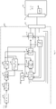
- Fig. 1 shows a modular structure of a power adapter provided by an exemplary embodiment of this disclosure. For description, only parts related to the exemplary embodiment of this disclosure are shown, and detailed description thereof is as follows:
- the power adapter 100 provided by the exemplary embodiment of this disclosure is coupled to the communication interface 20 of the electronic device 200 via the communication interface 10 thereof, and charges the battery 201 in the electronic device 200.
- the power adapter 100 comprises an EMI filter circuit 101, a high-voltage rectifier and filter circuit 102, an isolation transformer 103, an output filter circuit 104 and a voltage tracking and control circuit 105.
- the mains supply after the electromagnetic interference filter by the EMI filter circuit 101, is rectified and filtered by the high-voltage rectifier and filter circuit 102 to output a high-voltage direct current.
- the high-voltage direct current after electric isolation through the isolation transformer 103 is output to the output filter circuit 104 for filtering processing, and then charges the battery.
- the voltage tracking and control circuit 105 adjusts an output voltage of the isolation transformer 103 according to an output voltage of the output filter circuit 104.
- the power adapter 100 further comprises a power module 106, a main control module 107, a potential regulation module 108, a current detection module 109, a voltage detection module 110 and an output switch module 111.
- An input terminal of the power module 106 is coupled to a secondary terminal of the isolation transformer 103.
- a power terminal of the main control module 107, a power terminal of the potential regulation module 108, and a power terminal of the current detection module 109 are jointly coupled to an output terminal of the power module 106.
- a high-potential terminal of the main control module 107 and a high-potential terminal of the potential regulation module 108 are both coupled to a positive output terminal of the output filter circuit 104.
- a potential regulation terminal of the potential regulation module 108 is coupled to the voltage tracking and control circuit 105.
- a direct current input terminal of the current detection module 109 is coupled to the positive output terminal of the output filter circuit 104.
- a current detection feedback terminal of the current detection module 109 is coupled to a current detection terminal of the main control module 107.
- a clock output terminal and a data output terminal of the main control module 107 are coupled to a clock input terminal and a data input terminal of potential regulation module 108.
- a first detection terminal and a second detection terminal of the voltage detection module 110 are coupled to a direct current output terminal of the current detection module 109 and a negative output terminal of output filter circuit 104 respectively.
- a first output terminal and a second output terminal of the voltage detection module 110 are coupled to a first voltage detection terminal and a second voltage detection terminal of the main control module 107 respectively.
- An input terminal of the output switch module 111 is coupled to the direct current output terminal of the current detection module 109.
- An output terminal of the output switch module 111 and the negative output terminal of output filter circuit 104 are coupled with the communication interface 10.
- the output terminal of the output switch module 111 is also coupled to a third detection terminal of the voltage detection module 110.
- a ground terminal of output switch module 111 is coupled to the negative output terminal of the output filter circuit 104.
- a controlled terminal and the power terminal of the output switch module 111 are coupled to a switch control terminal of the main control module 107 and the secondary terminal of isolation transformer 103 respectively.
- the negative output terminal of the output filter circuit 104, the output terminal of output switch module 111, the first communication terminal and the second communication terminal of the main control module 107 are all coupled to the communication interface 10 of power adapter 100.
- the main control module 107 controls the output switch module 111 to switch off a direct current output of the power adapter 100, the voltage detection module 110 detects an output voltage of the power adapter 100 and feeds back a voltage detection signal to main control module 107, and the main control module 107 determines whether the output voltage of the power adapter 100 is greater than a voltage threshold (e.g., 2V) according to the voltage detection signal.
- a voltage threshold e.g., 2V
- the main control module 107 continues to judge the output voltage of power adapter 100; if the output voltage of the power adapter 100 is not greater than the voltage threshold, the main control module 107 controls the output switch module 111 to switch on the direct current output of the power adapter 100, and drives the voltage tracking and control circuit 105 through the potential regulation module 108 to set the output voltage of isolation transformer 103 as a conventional output voltage (e.g., 5.1V); the current detection module 109 detects an output current of the power adapter 100 and feeds back a current detection signal to the main control module 107.
- a conventional output voltage e.g., 5.1V
- the main control module 107 determines, according to the current detection signal, that the output current of the power adapter 100 is within a conventional current range for a preset time interval, the main control module 107 performs a quick charge inquiry communication with the electronic device 200. After the electronic device 200 sends a quick charge command to the main control module 107, the main control module 107, according to the battery voltage information fed back by electronic device 200, drives the voltage tracking and control circuit 105 through potential regulation module 108 to adjust the output voltage of the isolation transformer 103.
- the main control module 107 drives the voltage tracking and control circuit 105 through potential regulation module 108 to adjust the output voltage of isolation transformer 103, so that the power adapter 100 outputs direct current according to a quick charge current value (4A) and a quick charge voltage value (3.4V ⁇ 4.8V).
- the current detection module 109 continues to detect the output current of the power adapter 100 and feed back the current detection signal to the main control module 107 if the output current value of the power adapter 100 is less than a lower current limit (e.g., 1A); the main control module 107 controls the output switch module 111 to switch off the direct current output of the power adapter 100 for short-circuit protection if the output current value of power adapter 100 is greater than an upper current limit (e.g., 4A).
- a lower current limit e.g. 1A
- an upper current limit e.g. 4A
- the main control module 107 sends a quick charge inquiry command to the electronic device 200, the electronic device 200 judges whether the voltage of battery 201 reaches the quick charge voltage value according to the quick charge inquiry command, if yes, feeds back the quick charge command to the main control module 107, and if no, feeds back a quick charge rejecting command to the main control module 107.
- the main control module 107 drives the voltage tracking and control circuit 105 through the potential regulation module 108 to adjust the output voltage of the isolation transformer 103
- the main control module 107 sends a request for obtaining a battery voltage to the electronic device 200 according to the quick charge command sent by electronic device 200
- the electronic device 200 feeds back the battery voltage information to the main control module 107 according to the request for obtaining the battery voltage.
- the main control module 107 drives the voltage tracking and control circuit 105 through the potential regulation module 108 to adjust the output voltage of the isolation transformer 103 to the above predefined quick charge voltage.
- the main control module 107 drives the voltage tracking and control circuit 105 through the potential regulation module 108 to adjust the output voltage of the isolation transformer 103 as follows, so that the power adapter 100 outputs direct current according to the quick charge current value and the quick charge voltage value.
- the main control module 107 performs the quick charge inquiry communication with the electronic device 200.
- the main control module 107 feeds back the output voltage information to the electronic device 200; when the output voltage of power adapter 100 falls in the rated range of quick charge voltage or equals to the rated quick charge voltage, the electronic device 200 determines that the output voltage of power adapter 100 meets the voltage requirement for quick charge predefined by the electronic device 200, and feeds back a command for starting the quick charge mode to the main control module 107; according to the command for starting the quick charge mode, the main control module 107 drives the voltage tracking and control circuit 105 through the potential regulation module 108 to adjust the output voltage of the isolation transformer 103, so that the power adapter 100 outputs direct current according to the quick charge current value and the quick charge voltage value.
- the electronic device 200 sends a voltage bias feedback signal to the main control module 107; according to the voltage bias feedback signal, the main control module 107 drives the voltage tracking and control circuit 105 through the potential regulation module 108 to adjust the output voltage of the isolation transformer 103, and then continues to perform the quick charge inquiry communication with the electronic device 200.
- the voltage bias feedback signal includes a low-voltage feedback signal and a high-voltage feedback signal.
- the main control module 107 drives the voltage tracking and control circuit 105 through the potential regulation module 108 to raise the output voltage of the isolation transformer 103; if the voltage is higher, the main control module 107, according to the high-voltage feedback signal, drives the voltage tracking and control circuit 105 through the potential regulation module 108 to lower the output voltage of the isolation transformer 103.
- the main control module 107 drives the voltage tracking and control circuit 105 through the potential regulation module 108 to adjust the output voltage of the isolation transformer 103, so that the power adapter 100 outputs direct current according to the quick charge current value and the quick charge voltage value.
- the detailed process is as follows.
- the main control module 107 drives the voltage tracking and control circuit 105 through the potential regulation module 108 to adjust the output voltage of the isolation transformer 103, such that the output current and the output voltage of power adapter 100 are adjusted to the quick charge current value (e.g., 4A) and the quick charge voltage value (e.g., any value ranging from 3.4V to 4.8V) respectively.
- the quick charge current value e.g., 4A
- the quick charge voltage value e.g., any value ranging from 3.4V to 4.8V
- the main control module 107 obtains the battery voltage information from the electronic device 200, and determines, according to the voltage detection signal fed back by the voltage detection module 110, whether the difference between the output voltage of the power adapter 100 and the battery voltage exceeds a voltage difference threshold (e.g., 0.8V), if yes, it indicates that the line impedance between the power adapter 100 and the electronic device 200 or between the power adapter 100 and the battery 201 is abnormal, and the main control module 107 controls the output switch module 111 to switch off the direct current output of adapter 100; if no, the main control module 107, according to the battery voltage information, drives the voltage tracking and control circuit 105 through the potential regulation module 108 to adjust the output voltage of the isolation transformer 103, so as to adjust the output current of the power adapter 100, and continues to obtain the battery voltage information from the charging control module 300 so as to make cyclical adjustment to the output current of power adapter 100 during quick charge to the battery 201. In this way, the process of quick charge to the battery 201 can be optimized and the
- the main control module 107 drives the voltage tracking and control circuit 105 through the potential regulation module 108 to adjust the output voltage of the isolation transformer 103 so that the power adapter 100 outputs direct current according to the quick charge current value and the quick charge voltage value, meanwhile, the electronic device 200 detects the voltage of the battery 201. If the voltage of the battery 201 is greater than a quick charge voltage threshold (e.g., 4.35V), the electronic device 200 stops introducing direct current from the power adapter 100 for charging the battery 201, and feeds back a quick charge stop command to the main control module 107, and the main control module 107, according to the quick charge stop command, quits the quick charge mode and returns to the conventional charge mode.
- a quick charge voltage threshold e.g., 4.35V
- Fig. 2 shows an exemplary circuit of the above-mentioned power adapter 100. For description, it only shows the parts related to the exemplary embodiment of this disclosure, which is detailed as follows.
- the power module 106 includes: a first capacitor C1, a voltage stabilizing chip U1, a second capacitor C2, a first inductor L1, a second inductor L2, a first diode D1, a second diode D2, a third capacitor C3, a first resistor R1 and a second resistor R2.
- a junction of a first terminal of the first capacitor C1, and an input power pin Vin and an enable pin EN of the voltage stabilizing chip U1 is configured as the input terminal of the power module 106, a second terminal of the first capacitor C1 and a ground pin GND of the voltage stabilizing chip U1 are jointly grounded, a switch pin SW of the voltage stabilizing chip U1 and a first terminal of the second capacitor C2 are jointly coupled to a first terminal of first inductor L1, an internal switch pin BOOST of the voltage stabilizing chip U1 and a second terminal of the second capacitor C2 are jointly coupled to a cathode of the first diode D1, an voltage feedback pin FB of the voltage stabilizing chip U1 is coupled to a first terminal of the first resistor R1 and a first terminal of the second resistor R2, a second terminal of the first inductor L1 and a cathode of the second diode D2 are jointly coupled to a first terminal of the second inductor L2, a junction of a second terminal of the second inductor L
- the power module 106 performs the voltage conversion processing on the voltage at the secondary terminal of the isolation transformer 103 by using voltage stabilizing chip U1 as the core, and outputs +3.3V voltage to the main control module 107, the potential regulation module 108 and the current detection module 109.
- the voltage stabilizing chip U1 may specifically be an MCP16301 buck DC/DC converter.
- the main control module 107 includes: a main control chip U2, a third resistor R3, a reference voltage chip U3, a fourth resistor R4, a fifth resistor R5, a fourth capacitor C4, a sixth resistor R6, a seventh resistor R7, a first NMOS transistor Q1, an eighth resistor R8, a ninth resistor R9, a tenth resistor R10, an eleventh resistor R11, a twelfth resistor R12, a thirteenth resistor R13 and a fourteenth resistor R14.
- a power pin VDD of the main control chip U3 is configured as the power terminal of the main control module 107, a ground pin VSS of the main control chip U3 is grounded, a first input/output pin RA0 of the main control chip U3 is suspended, a first terminal of the third resistor R3 is coupled to the power pin VDD of the main control chip U3, a second terminal of the third resistor R3 and a first terminal of the fourth resistor R4 are jointly coupled to a cathode CATHODE of the reference voltage chip U3, an anode ANODE of the reference voltage chip U3 is grounded, a vacant pin NC of the reference voltage chip U3 is suspended, a second terminal of the fourth resistor R4 is coupled to a second input/output pin RA1 of the main control chip U2, a third input/output pin RA2 of the main control chip U2 is configured as the current detection terminal of the main control module 107, a fourth input/output pin RA3 of the main control chip U2 is coupled to a first
- a second terminal of the fourth capacitor C4 is grounded.
- a fifth input/output pin RA4 of the main control chip U2 is configured as the switch control terminal of the main control module 107.
- a sixth input/output pin RA5 of the main control chip U2 is coupled to a first terminal of the sixth resistor R6.
- a second terminal of the sixth resistor R6 and a gate electrode of the first NMOS transistor Q1 are jointly coupled to a first terminal of seventh resistor R7.
- a second terminal of the seventh resistor R7 and a source electrode of a first NMOS transistor Q1 are jointly grounded.
- a drain electrode of the first NMOS transistor Q1 is coupled to a first terminal of the eighth resistor R8.
- a second terminal of the eighth resistor R8 is configured as the high-potential terminal of the main control module 107.
- a seventh input/output pin RC0 and an eighth input/output pin RC1 of the main control chip U2 are configured as the clock output terminal and the data output terminal of the main control module 107 respectively.
- a tenth input/output pin RC3 and a ninth input/output pin RC2 of the main control chip U2 are configured as the first voltage detection terminal and the second voltage detection terminal of the main control module 107 respectively.
- An eleventh input/output pin RC4 and a twelfth input/output pin RC5 of the main control chip U2 are coupled to a first terminal of the ninth resistor R9 and a first terminal of the tenth resistor RIO respectively.
- a first terminal of an eleventh resistor R11 and a first terminal of the twelfth resistor R12 are coupled to a second terminal of the ninth resistor R9 and a second terminal of the tenth resistor RIO respectively.
- a second terminal of the eleventh resistor R11 and a second terminal of the twelfth resistor R12 are jointly grounded.
- a first terminal of the thirteenth resistor R13 and a first terminal of the fourteenth resistor R14 are coupled to a second terminal of the ninth resistor R9 and the second terminal of tenth resistor RIO respectively.
- a second terminal of the thirteenth resistor R13 and a second terminal of the fourteenth resistor R14 are jointly coupled to the power pin VDD of the main control chip U2.
- the second terminal of ninth resistor R9 and the second terminal of the tenth resistor RIO are configured as the first communication terminal and the second communication terminal of the main control module 107 respectively.
- the main control chip U2 may be a PIC12LF1822, PIC12F1822, PIC16LF1823 or PIC16F1823 single chip microcomputer
- reference voltage chip U3 may be an LM4040 voltage reference device.
- the potential regulation module 108 includes: a fifteenth resistor R15, a sixteenth resistor R16, a digital potentiometer U4, a seventeenth resistor R17, an eighteenth resistor R18, a fifth capacitor C5, a sixth capacitor C6 and a nineteenth resistor R19.
- a junction of a first terminal of fifteenth resistor R15, a first terminal of sixteenth resistor R16, a power pin VDD of the digital potentiometer U4 and a first terminal of the fifth capacitor C5 is configured as the power terminal of the potential regulation module 108.
- a second terminal of the fifth capacitor C5, a first terminal of the sixth capacitor C6, a ground pin VSS of the digital potentiometer U4 and a first terminal of the seventeenth resistor R17 are jointly grounded.
- a second terminal of the sixth capacitor C6 is coupled to the power pin VDD of the digital potentiometer U4.
- a junction of a second terminal of the fifteenth resistor R15 and a serial data pin SDA of the digital potentiometer U4 is configured as the data input terminal of the potential regulation module 108.
- a junction of a second terminal of the sixteenth resistor R16 and a clock input pin SCL of the digital potentiometer U4 is configured as the clock input terminal of the potential regulation module 108.
- An address zero pin A0 of the digital potentiometer U4 is grounded.
- a first potential wiring pin P0A of the digital potentiometer U4 and a first terminal of eighteenth resistor R18 are jointly coupled to a second terminal of the seventeenth resistor R17.
- a second terminal of the eighteenth resistor R18 and a second potential wiring pin P0B of the digital potentiometer U4 are jointly coupled to a first terminal of nineteenth resistor R19.
- a second terminal of the nineteenth resistor R19 is configured as the high-potential terminal of the potential regulation module 108.
- a potential tap pin P0W of digital potentiometer U4 is configured as the potential regulation terminal of the potential regulation module 108. Specifically, the digital potentiometer U4 adjusts an internal slide rheostat according to the clock signal and the data signal output from the main control chip U2 so as to change the potential at the tap terminal of the internal slide rheostat (i.e., the potential tap pin P0W of the digital potentiometer U4), such that the voltage tracking and control circuit 104 adjusts the output voltage of the isolation transformer 103 by following the potential change.
- the digital potentiometer U4 may specifically be an MCP45X1 digital potentiometer.
- the current detection module 109 includes: a twentieth resistor R20, a twenty-first resistor R21, a twenty-second resistor R22, a seventh capacitor C7, an eighth capacitor C8, a current detection chip U5, a twenty-third resistor R23, a ninth capacitor C9, a tenth capacitor C10 and a twenty-fourth resistor R24.
- a first terminal and a second terminal of twentieth resistor R20 are configured as the direct current input terminal and the direct current output terminal of current detection module 109 respectively, a first terminal of the twenty-first resistor R21 and a first terminal of the twenty-second resistor R22 are coupled to the first terminal and the second terminal of twentieth resistor R20 respectively, a second terminal of the twenty-first resistor R21 and a first terminal of seventh capacitor C7 are jointly coupled to a positive input pin IN+ of the current detection chip U5, a second terminal of the twenty-second resistor R22 and a first terminal of the eighth capacitor C8 are jointly coupled to a negative input pin IN- of the current detection chip U5, a junction of a power pin V+ of the current detection chip U5 and a first terminal of the ninth capacitor C9 is configured as the power terminal of the current detection module 109, a vacant pin NC of the current detection chip U5 is suspended, an output pin OUT of the current detection chip U5 is coupled to a first terminal of the twenty-third resistor R23, a second terminal
- the twentieth resistor R20 samples the output current of the output filter circuit 104 (i.e., the output current of the power adapter 100). Then, the current detection chip U5 outputs a current detection signal to the main control chip U2 according to the voltage across two terminals of the twentieth resistor R20, in which the current detection chip U5 may specifically be an INA286 current shunt monitor.
- the voltage detection module 110 includes: a twenty-fifth resistor R25, a twenty-sixth resistor R26, an eleventh capacitor C11, a twelfth capacitor C12, a twenty-seventh resistor R27 and a twenty-eighth resistor R28.
- a first terminal of the twenty-fifth resistor R25 is configured as the first detection terminal of the voltage detection module 110, a junction of a second terminal of the twenty-fifth resistor R25, a first terminal of the twenty-sixth resistor R26 and a first terminal of the eleventh capacitor C11 is configured as the second output terminal of the voltage detection module 110, a second terminal of the twenty-sixth resistor R26 is configured as the second detection terminal of the voltage detection module 110, a second terminal of eleventh capacitor C11, a first terminal of the twelfth capacitor C12 and a first terminal of the twenty-seventh resistor R27 are jointly coupled to a second terminal of the twenty-sixth resistor R26, a junction of a second terminal of the twelfth capacitor C12, a second terminal of the twenty-seventh resistor R27 and a first terminal of the twenty-eighth resistor R28 is configured as the first output terminal of the voltage detection module 110, and a second terminal of the twenty-eight
- the output switch module 111 includes: a twenty-ninth resistor R29, a thirtieth resistor R30, a thirteenth capacitor C13, a thirty-first resistor R31, a first NPN triode N1, a thirty-second resistor R32, a second NPN triode N2, a third diode D3, a voltage stabilizing diode ZD, a thirty-third resistor R33, a thirty-fourth resistor R34, a thirty-fifth resistor R35, a second NMOS transistor Q2 and a third NMOS transistor Q3.
- a first terminal of the twenty-ninth resistor R29 is configured as the controlled terminal of the output switch module 111, a second terminal of the twenty-ninth resistor R29 and a first terminal of the thirtieth resistor R30 are jointly coupled to a base electrode of the first NPN triode N1, a first terminal of the thirteenth capacitor C13, a first terminal of the thirty-first resistor R31 and a first terminal of the thirty-second resistor R32 are jointly coupled to a cathode of the third diode D3, an anode of the third diode D3 is configured as the power terminal of the output switch module 111, a second terminal of the thirty-first resistor R31 and a base electrode of the second NPN triode N2 are jointly coupled to a collector electrode of the first NPN triode N1, a second terminal of the thirty-second resistor R32, a cathode of the voltage stabilizing diode ZD and a first terminal of the thirty-third resistor R33 are jointly coupled to a collector electrode
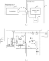
- Fig. 3 shows a schematic block diagram of a charging apparatus for an electronic device provided by an exemplary embodiment of this disclosure. For illustration, it only shows parts related to the exemplary embodiment of this disclosure, which is detailed as follows.
- the charging apparatus for the electronic device includes a power adapter 1 and a charging control module 2.
- the power adapter 1 is coupled to a communication interface 20 of the electronic device 3 via a communication interface 10, and charges a battery 31 in the electronic device.
- the charging control module 2 is built in the electronic device 3, and is coupled to the power adapter 1 via the communication interface 20 of the electronic device 3.
- the structure of the power adapter 1 is the same as that of the power adapter 100 as shown in Figs. 1-2 , and thus will not be elaborated herein.
- the main control module 107 controls the output switch module 111 to switch off the direct current output of the power adapter 1
- the voltage detection module 110 detects the output voltage of the power adapter 1 and feeds back a voltage detection signal to the main control module 107
- the main control module 107 judges whether the output voltage of the power adapter 1 is greater than the voltage threshold (e.g., 2V) according to the voltage detection signal. If the output voltage of the power adapter 1 is greater than the voltage threshold, the main control module 107 continues to judge the output voltage of the power adapter 1.
- the voltage threshold e.g. 2V
- the main control module 107 controls the output switch module 111 to switch on the direct current output of the power adapter 1, and drives the voltage tracking and control circuit 105 through the potential regulation module 108 to set the output voltage of isolation transformer 103 as the conventional output voltage (e.g., 5.1V).
- the current detection module 109 detects the output current of the power adapter 100, and feeds back a current detection signal to the main control module 107.
- the main control module 107 determines according to the above current detection signal that the output current of the power adapter 1 falls in the conventional current range for a preset time interval, the main control module 107 performs quick charge inquiry communication with the charging control module 2.
- the main control module 107 After the electronic device 200 sends a quick charge command to the main control module 107, the main control module 107, according to the battery voltage information fed back by the charging control module 2, drives the voltage tracking and control circuit 105 through the potential regulation module 108 to adjust the output voltage of the isolation transformer 103, and if the output voltage of the power adapter 1 meets the voltage requirement for quick charge predefined by the charging control module 2, the main control module 107 drives the voltage tracking and control circuit 105 through the potential regulation module 108 to adjust the output voltage of the isolation transformer 103, so that the power adapter 100 outputs direct current according to the quick charge current value (4A) and the quick charge voltage value (3.4V ⁇ 4.8V). In the meantime, the charging control module 2 introduces direct current from the power adapter 1 through the communication interface 20 of the electronic device 3 to charge the battery 31.
- Fig. 4 shows an exemplary circuit of the above-mentioned charging control module 2. For illustration, it only shows parts related to the exemplary embodiment of this disclosure, which is detailed as follows.
- the charging control module 2 includes: a battery connector J1, a main controller U6, a thirteenth capacitor C13, a thirty-sixth resistor R36, a thirty-seventh resistor R37, a fourteenth capacitor C14, a first Schottky diode SD1, a second Schottky diode SD2, a fifteenth capacitor C15, a thirty-eighth resistor R38, a thirty-ninth resistor R39, a fortieth resistor R40, a third NPN triode N3, a fourth NMOS transistor Q4 and a fifth NMOS transistor Q5.
- the battery connector J1 is coupled to multiple electrodes of the battery 300, a first pin 5A-1 and a second pin 5A-2 of the battery connector J1 are jointly grounded, a first ground pin GND1 and a second ground pin GND2 of the battery connector J1 are jointly grounded, a first input/output pin RA0 of the main controller U6 is coupled to a seventh pin 5A-3 and an eighth pin 5A-4 of the battery connector J1, a second input/output pin RA1, a seventh input/output pin RC0, an eighth input/output pin RC1 and a ninth input/output pin RC2 of the main controller U6 are coupled to a sixth pin 2A-4, a fifth pin 2A-3, a fourth pin 2A-2 and a third pin 2A-1 of the battery connector J1 respectively, an analog ground pin VSS and a ground pin GND of the main controller U6 are both grounded, a first vacant pin NC0 and a second vacant pin NC1 of the main controller U6 are suspended, a power pin VDD
- the main controller U6 may specifically be a PIC12LF1501, PIC12F1501, PIC16LF1503, PIC16F1503, PIC16LF1507, PIC16F1507, PIC16LF1508, PIC16F1508, PIC16LF1509 or PIC16F1509 single chip microcomputer.
- the charging control module 2 introduces direct current from the power adapter 1 through the communication interface 20 of the electronic device 3 to charge the battery 31, which is realized as follows.
- the main controller U6 outputs a control signal through its fifth input/output pin RA4 for controlling the fourth NMOS transistor Q4 and the fifth NMOS transistor Q5 to switch on, and controls the third NPN triode N3 to switch off through its tenth input/output pin RC3, so as to introduce direct current from the communication interface 10 of the power adapter 1 through a data cable for charging the battery 31.
- the direct current introduced by the charging control module 2 can further increase the current charging the battery 31, thus enabling the quick charge to the battery 31.
- the main controller U6 controls the fourth NMOS transistor Q4 and the fifth NMOS transistor Q5 to turn off by outputting a low level through its fifth input/output pin RA4, and controls the third NPN triode N3 to turn on by outputting a high level through its tenth input/output pin RC3.
- the main controller U6 performs the data communication with the electronic device through its fourth input/output Pin RA3 and eleventh input/output Pin RC4.
- the main controller U6 can transmit the voltage and electric quantity information of the battery 31 to the electronic device (e.g., mobile phone), and can also determine whether the quick charge process for the battery 31 has been completed according to the voltage of battery 31. If the quick charge process for the battery 31 has been completed, the main controller U6 may feed back a quick charge stop command to inform the electronic device to switch to the conventional charge mode from the quick charge mode.
- the main controller U6 detects the voltage of the battery 31 through the battery connector J1, and feeds back a charge stop command to inform the electronic device 3 to switch off the communication interface 20, so as to terminate the charge process for the battery 31.
- the electronic device 3 may, in the case of abnormal temperature, inform the main controller U6 to switch off the fourth NMOS transistor Q4 and the fifth NMOS transistor Q5 for stopping the quick charge to the battery 31, and meanwhile the electronic device 3 may switch to the conventional charge mode from the quick charge mode.
- the power adapter 1 works in the quick charge mode and the charging control module 2 introduces direct current from the power adapter 1 to charge the battery 31 if the power line VBUS and the ground line GND of the communication interface 10 of the power adapter 1 are coupled to the ground line GND and the power line VBUS of the communication interface 20 of the electronic device 3 respectively (i.e., the power line VBUS and the ground line GND of the communication interface 10 of power adapter 1 are coupled to the ground terminal of the charging control module 2 and the source electrode of the fifth NMOS transistor Q5 respectively), which means that the communication interface 10 of the power adapter 1 is reversely coupled to the communication interface 20 of the electronic device 3, direct current is coupled to the ground terminal of charging control module 2, and the source electrode of fifth NMOS transistor Q5 is grounded.
- the charging control module 2 may further include a sixth NMOS transistor Q6, a seventh NMOS transistor Q7 and a forty-first resistor R41.
- a source electrode of the sixth NMOS transistor Q6 is coupled to a source electrode of the fifth NMOS transistor Q5.
- a drain electrode of the sixth NMOS transistor Q6 is coupled to a drain electrode of the seventh NMOS transistor Q7.
- a source electrode of the seventh NMOS transistor Q7 is coupled to the collector electrode of the third NPN triode N3.
- a gate electrode of the sixth NMOS transistor Q6 and a gate electrode of the seventh NMOS transistor Q7 are jointly coupled to a first terminal of the forty-first resistor R41.
- a second terminal of the forty-first resistor R41 is grounded.
- the second terminal of the forty-first resistor R41 is coupled to direct current via the ground for driving the sixth NMOS transistor Q6 and the seventh NMOS transistor Q7 to switch off, which prevents the direct current that flows into the charging control module 2 from the ground from forming a loop, thereby protecting components in the charging control module 2 from any damage.
- the power adapter including the power module, the main control module, the potential regulation module, the current detection module, the voltage detection module and the output switch module, if the output current value of the power adapter falls within the conventional current range for the preset time interval during the process in which the power adapter charges the battery in the conventional charge mode after the power adapter is powered on or reset, the power adapter performs the quick charge inquiry communication with the electronic device, and after the electronic device sends the quick charge command to the power adapter, the power adapter adjusts the output voltage according to the battery voltage information fed back by the electronic device, and if this output voltage meets the voltage requirements for quick charge predefined by the electronic device, the power adapter adjusts its output current and output voltage according to the quick charge mode for charging the battery, such that the quick charge to the battery is realized, thereby shortening the charging time.
Landscapes
- Engineering & Computer Science (AREA)
- Power Engineering (AREA)
- Charge And Discharge Circuits For Batteries Or The Like (AREA)
- Dc-Dc Converters (AREA)
- Secondary Cells (AREA)
- Rectifiers (AREA)
Claims (9)
- Stromversorgungsadapter (100), der dafür ausgelegt ist, mit einer Kommunikationsschnittstelle (20) einer Elektronikvorrichtung (200) über eine
Kommunikationsschnittstelle (10) davon verbunden zu werden und eine Batterie (201) in der Elektronikvorrichtung (200) zu laden, wobei der Stromversorgungsadapter (100) eine EMV-Filterschaltung (101), eine Hochspannungsgleichrichterund -filterschaltung (102), einen Isolationstransformator (103), eine Ausgangsfilterschaltung (104) und eine Spannungsverfolgungs- und -steuerschaltung (105) umfasst, dadurch gekennzeichnet, dass der Stromversorgungsadapter (100) ferner Folgendes umfasst:- ein Leistungsmodul (106) mit einem Eingangsanschluss, der mit einem Sekundäranschluss des Isolationstransformators (103) gekoppelt ist;- ein Hauptsteuermodul (107),- ein Potentialregelungsmodul (108) mit einem Potentialregelungsanschluss, der mit der Spannungsverfolgungs- und -steuerschaltung (105) zwecks Potentialregelung gekoppelt ist, und mit
einem Hochpotentialanschluss, der mit einem Hochpotentialanschluss des Hauptsteuermoduls (107) und einem positiven Ausgangsanschluss der Ausgangsfilterschaltung (104) gekoppelt ist,- ein Stromdetektionsmodul (109) mit einem Gleichstromeingangsanschluss und gekoppelt mit einem positiven Ausgangsanschluss der Ausgangsfilterschaltung (104) zum Eingeben einer Gleichstromeingabe und mit einem Stromdetektionsrückkopplungsanschluss, der mit dem Hauptsteuermodul (107) zum Detektieren und Rückkoppeln eines Stroms gekoppelt ist,- ein Spannungsdetektionsmodul (110), das mit einem Gleichstromausgangsanschluss des Stromdetektionsmoduls (109) über einen ersten Detektionsanschluss, mit einem negativen Ausgangsanschluss der Ausgangsfilterschaltung (104) über einen zweiten Detektionsanschluss und mit dem Hauptsteuermodul (107) über einen ersten und einen zweiten Spannungsdetektionsanschluss gekoppelt ist, und- ein Ausgangsschaltmodul (111) mit einem Eingangsanschluss, der mit dem Gleichstromausgangsanschluss des Stromdetektionsmoduls (109) gekoppelt ist, mit einem Ausgangsanschluss, der mit einem dritten Detektionsanschluss des Spannungsdetektionsmoduls (110) gekoppelt ist, mit einem Masseanschluss, derwobei ein Schaltsteueranschluss des Hauptsteuermoduls (107) mit einem gesteuerten Anschluss des Ausgangsschaltmoduls (111) gekoppelt ist, wobei Leistungsanschlüsse des Hauptsteuermoduls (107), des Potentialregelungsmoduls (108) und des Stromdetektionsmoduls (109) mit einem Ausgangsanschluss des Leistungsmoduls (106) gekoppelt sind, wobei jeder von einem negativen Ausgangsanschluss der Ausgangsfilterschaltung (104), dem Ausgangsanschluss des Ausgangsschaltmoduls (111) und eines ersten Kommunikationsanschlusses und eines zweiten Kommunikationsanschlusses des Hauptsteuermoduls (107) mit der Kommunikationsschnittstelle (10) des Stromversorgungsadapters gekoppelt sind, und
mit einem negativen Ausgangsanschluss der Ausgangsfilterschaltung (104) gekoppelt ist, und mit einem Leistungsanschluss, der mit dem Sekundäranschluss des Isolationstransformators (103) gekoppelt ist;
wobei das Hauptsteuermodul (107) ausgelegt ist zum- Laden der Batterie (201), nachdem der Stromversorgungsadapter (100) eingeschaltet oder zurückgesetzt wurde, um das Spannungsdetektionsmodul (110) zu steuern, die Ausgangsspannung des Stromversorgungsadapters zu detektieren und ein Spannungsdetektionssignal an das Hauptsteuermodul (107) zurück zu koppeln, um zu bestimmen, ob die Ausgangsspannung des Stromversorgungsadapters größer als eine Spannungsschwelle ist gemäß dem Spannungsdetektionssignal; und- wenn die Ausgangsspannung des Stromversorgungsadapters (100) größer als die Spannungsschwelle ist, Fortsetzen des Beurteilens der Ausgangsspannung des Stromversorgungsadapters (100);- wenn die Ausgangsspannung des Stromversorgungsadapters (100) nicht größer als die Spannungsschwelle ist, Steuern des Ausgangsschaltmoduls (111), den Gleichstromausgang des Stromversorgungsadapters (100) einzuschalten und zum Ansteuern der Spannungsverfolgungs- und -steuerschaltung (105) durch das Potentialregelungsmodul (108), eine Ausgangsspannung des Isolationstransformators (103) als eine herkömmliche Ausgangsspannung einzustellen, wobei das Stromdetektionsmodul (109) ausgelegt ist zum Detektieren des Ausgangsstroms des Stromversorgungsadapters (100), und zum Rückkoppeln eines Stromdetektionssignals an das Hauptsteuermodul (107) ;- wenn das Hauptsteuermodul (107) bestimmt, gemäß dem Stromdetektionssignal, dass der Ausgangsstrom des Stromversorgungsadapters für ein voreingestelltes Zeitintervall innerhalb eines herkömmlichen Strombereichs liegt, Durchführen einer Schnellladung-Anfragekommunikation mit der Elektronikvorrichtung (200); und, nachdem die Elektronikvorrichtung (200) einen Schnellladungsbefehl an das Hauptsteuermodul (107) gesendet hat, Ansteuern der Spannungsverfolgungs- und -steuerschaltung (105) durch das Potentialregelungsmodul (108) zum Einstellen der Ausgangsspannung des Isolationstransformators (103) gemäß Batteriespannungsinformationen, die von der Elektronikvorrichtung (200) zurückgemeldet wurden;- wenn die Ausgangsspannung des Stromversorgungsadapters (100) eine durch die Elektronikvorrichtung (200) definierte Spannungsanforderung für Schnellladung erfüllt, Ansteuern der Spannungsverfolgungsund - steuerschaltung (105) durch das Potentialregelungsmodul (108) zum Einstellen der Ausgangsspannung des Isolationstranformators (103), so dass der Stromversorgungsadapter (100) gemäß einem Schnellladungsstromwert und einem Schnellladungsspannungswert Gleichstrom ausgibt. - Stromversorgungsadapter (100) nach Anspruch 1, wobei, während der Schnellladung-Anfragekommunikation, das Hauptsteuermodul (107) ausgelegt ist zum Senden eines Schnellladung-Anfragebefehls an die Elektronikvorrichtung (200), so dass die Elektronikvorrichtung (200) bestimmt, ob eine Spannung der Batterie den Schnellladung-Spannungswert gemäß dem Schnellladung-Anfragebefehl erreicht, den Schnellladungsbefehl an das Hauptsteuermodul (107) zurückmeldet, wenn die Spannung der Batterie den Schnellladung-Spannungswert erreicht, und einen Schnellladung-Ablehnungsbefehl an das Hauptsteuermodul (107) zurückmeldet, wenn die Spannung der Batterie den Schnellladung-Spannungswert nicht erreicht.
- Stromversorgungsadapter (100) nach Anspruch 2, wobei, wenn die Elektronikvorrichtung (200) bestimmt, dass die Ausgangsspannung des Stromversorgungsadapters (100) die Spannungsanforderung für Schnellladung nicht erfüllt, die Elektronikvorrichtung (200) ausgelegt ist zum Senden eines Vorspannungsrückmeldesignals an das Hauptsteuermodul (107), und das Hauptsteuermodul (107) ausgelegt ist zum Ansteuern der Spannungsverfolgungsund -steuerschaltung durch das Potentialregelungsmodul (108), die Ausgangsspannung des Isolationstransformators (103) einzustellen und Durchführen der Schnellladung-Anfragekommunikation mit der Elektronikvorrichtung (200) fortzuführen.
- Stromversorgungsadapter (100) nach einem der Ansprüche 1 bis 3, wobei, nach dem Empfangen des Befehls zum Starten des Schnellladungsmodus, das Hauptsteuermodul (107) ausgelegt ist zum Ansteuern der Spannungsverfolgungs- und -steuerschaltung (105) durch das Potentialregelungsmodul (108), die Ausgangsspannung des Isolationstransformators derart einzustellen, dass die Ausgangsspannung und der Ausgangsstrom des Stromversorgungsadapters jeweils auf den SchnellladungSpannungswert und den Schnellladung-Stromwert eingestellt sind;
das Hauptsteuermodul (107) ausgelegt ist zum Erhalten der Batteriespannungsinformationen von der Elektronikvorrichtung (200) in Echtzeit und zum Bestimmen, gemäß einem durch das Spannungsdetektionsmodul in Echtzeit zurückgekoppelten Spannungsrückkopplungssignal, ob eine Spannungsdifferenz zwischen der Spannung der Batterie und der Ausgangsspannung des Stromversorgungsadapters größer als eine Spannungsdifferenzschwelle ist;
wenn die Spannungsdifferenz zwischen der Spannung der Batterie (201) und der Ausgangsspannung des Stromversorgungsadapters (100) größer als die Spannungsdifferenzschwelle ist, ist das Hauptsteuermodul (107) ausgelegt zum Steuern des Ausgangsschaltmoduls (104), die Gleichstromausgabe des Stromversorgungsadapters (100) auszuschalten; und,
wenn die Spannungsdifferenz zwischen der Spannung der Batterie (201) und der Ausgangsspannung des Stromversorgungsadapters (100) kleiner oder gleich der Spannungsdifferenzschwelle ist, ist das Hauptsteuermodul (107) ausgelegt zum Steuern der Spannungsverfolgungs- und -steuerschaltung (105) durch das Potentialregelungsmodul (108), die Ausgangsspannung des Isolationstransformators (103) gemäß den Batteriespannungsinformationen einzustellen, um somit den Ausgangsstrom des Stromversorgungsadapters einzustellen. - Stromversorgungsadapter (100) nach einem der Ansprüche 1 bis 4, wobei der Schnellladung-Stromwert 4 A beträgt und der Schnellladung-Spannungswert ein beliebiger zwischen 3,4 V und 4,8 V ausgewählter Wert ist.
- Stromversorgungsadapter (100) nach einem der Ansprüche 1 bis 5, wobei, während der Stromversorgungsadapter die Batterie gemäß dem Schnellladung-Spannungswert und dem SchnellladungStromwert lädt, die Elektronikvorrichtung (200) dafür ausgelegt ist, Einspeisen von Gleichstrom von dem Stromversorgungsadapter (100) zu stoppen und einen Schnellladung-Stoppbefehl an das Hauptsteuermodul (107) zurückzumelden, wenn die Spannung der Batterie (201) größer als eine Schnellladung-Spannungsschwelle ist, und das Hauptsteuermodul (107) ausgelegt ist zum Steuern des Stromversorgungsadapters (100), gemäß dem Schnellladung-Stoppbefehl, von einem Schnellladungsmodus in einen herkömmlichen Ladungsmodus zu schalten.
- Ladeeinrichtung für eine Elektronikvorrichtung (3), umfassend einen Stromversorgungsadapter (1) nach einem der Ansprüche 1 bis 6 und ein Ladesteuerungsmodul (2), das in die Elektronikvorrichtung (3) eingebaut ist und mit dem Stromversorgungsadapter (3) über die Kommunikationsschnittstelle (20) der Elektronikvorrichtung (3) gekoppelt ist.
- System, umfassend
eine Elektronikvorrichtung (3), die eine Kommunikationsschnittstelle (20), ein Ladesteuerungsmodul (2) und eine Batterie (31) umfasst,
wobei:- jedes des Ladesteuerungsmoduls (2) und der Batterie (31) mit einer Kommunikationsschnittstelle (10) eines Stromversorgungsadapters (1) über die Kommunikationsschnittstelle (20) der Elektronikvorrichtung gekoppelt ist, so dass der Stromversorgungsadapter (1) mit dem Ladesteuerungsmodul (2) kommuniziert und die Batterie (31) lädt;- das Ladesteuerungsmodul (2) ferner an eine Elektrode der Batterie (31) gekoppelt ist und ausgelegt ist zum Detektieren einer Spannung der Batterie (31);- das Ladesteuerungsmodul (2) ferner ausgelegt ist zum Bestimmen, ob die Batterie eine Schnellladebedingung erfüllt, nachdem eine Schnellladung-Anfragenachricht von dem Stromversorgungsadapter empfangen wurde, und zum Rückmelden eines Schnellladebefehls und von Batteriespannungsinformationen an den Stromversorgungsadapter (1), wenn die Batterie (31) die Schnellladebedingung erfüllt;- das Ladesteuerungsmodul (2) ferner ausgelegt ist zum Empfangen von durch den Stromversorgungsadapter (1) gesendeten Ausgangsspannungsinformationen, um zu bestimmen, ob eine Ausgangsspannung des Stromversorgungsadapters eine voreingestellte Spannungsanforderung für Schnellladung gemäß den Ausgangsspannungsinformationen erfüllt, und zum Senden eines Befehls zum Starten einer Schnellladung an den Stromversorgungsadapter, wenn die Ausgangsspannung des Stromversorgungsadapters (1) die voreigenstellte Spannungsanforderung für Schnellladung erfüllt, und einen Stromversorgungsadapter (100) nach einem der 20 Ansprüche 1 bis 6. - System nach Anspruch 8, wobei das Ladesteuerungsmodul (2) ferner ausgelegt ist zum Stoppen des Einspeisens von Gleichstrom von dem Stromversorgungsadapter (1) und zum Senden eines Schnellladung-Stoppbefehls an den Stromversorgungsadapter (1) zum Umschalten aus einem Schnelllademodus in einen herkömmlichen Lademodus, wenn die Spannung der Batterie (31) größer als eine 30 Schnellladung-Spannungsschwelle ist.
Applications Claiming Priority (2)
| Application Number | Priority Date | Filing Date | Title |
|---|---|---|---|
| CN201410043062.0A CN103762702B (zh) | 2014-01-28 | 2014-01-28 | 电子设备充电装置及其电源适配器 |
| PCT/CN2014/077284 WO2015113341A1 (zh) | 2014-01-28 | 2014-05-12 | 电子设备充电装置及其电源适配器 |
Publications (3)
| Publication Number | Publication Date |
|---|---|
| EP3101766A1 EP3101766A1 (de) | 2016-12-07 |
| EP3101766A4 EP3101766A4 (de) | 2017-12-27 |
| EP3101766B1 true EP3101766B1 (de) | 2020-06-17 |
Family
ID=50529891
Family Applications (1)
| Application Number | Title | Priority Date | Filing Date |
|---|---|---|---|
| EP14880925.4A Active EP3101766B1 (de) | 2014-01-28 | 2014-05-12 | Ladevorrichtung für elektronische vorrichtung und leistungsadapter für elektronische vorrichtung |
Country Status (9)
| Country | Link |
|---|---|
| US (3) | US10224725B2 (de) |
| EP (1) | EP3101766B1 (de) |
| JP (3) | JP6239777B2 (de) |
| KR (2) | KR101855793B1 (de) |
| CN (1) | CN103762702B (de) |
| AU (1) | AU2014381131B2 (de) |
| MY (1) | MY192951A (de) |
| SG (1) | SG11201606226SA (de) |
| WO (1) | WO2015113341A1 (de) |
Families Citing this family (61)
| Publication number | Priority date | Publication date | Assignee | Title |
|---|---|---|---|---|
| FI20140021L (fi) * | 2014-01-27 | 2015-07-28 | Asmo Saloranta | Akkulaturi |
| CN104810909B (zh) * | 2014-01-28 | 2016-09-28 | 广东欧珀移动通信有限公司 | 快速充电控制方法和系统 |
| CN106532884B (zh) | 2014-01-28 | 2019-07-19 | Oppo广东移动通信有限公司 | 电池充电装置及方法 |
| DK3101770T3 (da) | 2014-01-28 | 2019-07-22 | Guangdong Oppo Mobile Telecommunications Corp Ltd | Strømadapter og terminal |
| WO2015113461A1 (zh) | 2014-01-28 | 2015-08-06 | 广东欧珀移动通信有限公司 | 电源适配器和终端 |
| CN104810873B (zh) | 2014-01-28 | 2018-03-16 | 广东欧珀移动通信有限公司 | 电子设备充电控制装置及方法 |
| DK3101437T3 (da) | 2014-01-28 | 2019-05-06 | Guangdong Oppo Mobile Telecommunications Corp Ltd | Strømadapter, terminal og fremgangsmåde til håndtering af impedansafvigelse i en opladningssløjfe |
| CN105098862A (zh) * | 2014-05-19 | 2015-11-25 | 中兴通讯股份有限公司 | 一种充电控制方法、装置及终端 |
| CN105334420B (zh) * | 2014-06-27 | 2020-02-04 | 联想(北京)有限公司 | 一种信息处理方法及电子设备 |
| KR102320853B1 (ko) | 2014-09-02 | 2021-11-02 | 삼성전자 주식회사 | 전자 장치, 전자 장치의 충전 제어 방법, 전원 공급 장치, 및 전원 공급 장치의 전력 공급 방법 |
| US10203803B2 (en) * | 2014-09-02 | 2019-02-12 | Apple Inc. | Touch scan modes during device charging |
| CN105576727B (zh) * | 2014-10-16 | 2020-02-28 | 中兴通讯股份有限公司 | 一种快速充电的方法、装置和系统 |
| CN104269585B (zh) * | 2014-10-17 | 2016-09-28 | 广东欧珀移动通信有限公司 | 一种充电方法和移动终端 |
| BR112016028206B1 (pt) * | 2014-11-11 | 2022-03-29 | Guangdong Oppo Mobile Telecommunications Corp., Ltd | Terminal, e, adaptador de energia |
| CN108667094B (zh) * | 2014-11-11 | 2020-01-14 | Oppo广东移动通信有限公司 | 通信方法、电源适配器和终端 |
| PT3131171T (pt) * | 2014-11-11 | 2019-03-18 | Guangdong Oppo Mobile Telecommunications Corp Ltd | Adaptador de alimentação, terminal e sistema de carregamento |
| US20170244265A1 (en) * | 2014-11-11 | 2017-08-24 | Guangdong Oppo Mobile Telecommunications Corp., Ltd. | Communication method, power adaptor and terminal |
| CN105811506B (zh) * | 2014-12-24 | 2019-12-27 | Oppo广东移动通信有限公司 | 用于为电子设备充电的方法和电子设备 |
| CN105762884B (zh) * | 2014-12-24 | 2020-01-17 | Oppo广东移动通信有限公司 | 用于为电子设备充电的方法和电子设备 |
| CN104600796B (zh) * | 2014-12-30 | 2019-09-20 | 惠州Tcl移动通信有限公司 | 快速充电的移动终端及方法、系统 |
| EP3091633B1 (de) * | 2015-05-07 | 2018-02-07 | Richtek Technology Corporation | Adaptiver leistungswandler eines mobilen ladegeräts |
| ES2721053T3 (es) * | 2015-05-13 | 2019-07-26 | Guangdong Oppo Mobile Telecommunications Corp Ltd | Método de carga rápida, adaptador de alimentación y terminal móvil |
| CN106063073B (zh) * | 2015-05-13 | 2018-09-28 | 广东欧珀移动通信有限公司 | 快速充电方法、电源适配器和移动终端 |
| CN106410303B (zh) * | 2015-07-27 | 2019-02-19 | 小米科技有限责任公司 | 充电方法及装置 |
| CN107276394B (zh) * | 2015-09-14 | 2019-07-16 | Oppo广东移动通信有限公司 | 一种智能直流转换装置及应用系统 |
| CN105244980B (zh) * | 2015-11-20 | 2017-10-17 | 深圳市祝你快乐科技有限公司 | 一种基于手机app控制的节能充电器 |
| WO2017088138A1 (zh) * | 2015-11-26 | 2017-06-01 | 广东欧珀移动通信有限公司 | 移动终端的充电装置 |
| WO2017117730A1 (zh) | 2016-01-05 | 2017-07-13 | 广东欧珀移动通信有限公司 | 快速充电方法、移动终端和适配器 |
| US10170923B2 (en) | 2016-01-12 | 2019-01-01 | Richtek Technology Corporation | Adaptive buck converter with monitor circuit and charging cable using the same |
| US9979214B2 (en) * | 2016-01-12 | 2018-05-22 | Richtek Technology Corporation | Adaptive buck converter and charging cable using the same |
| KR101906977B1 (ko) * | 2016-02-05 | 2018-10-11 | 광동 오포 모바일 텔레커뮤니케이션즈 코포레이션 리미티드 | 충전 방법, 어댑터 및 이동 단말기 |
| EP3285364B1 (de) | 2016-02-05 | 2020-02-26 | Guangdong Oppo Mobile Telecommunications Corp., Ltd. | Adapter und ladesteuerungsverfahren |
| CN106019170B (zh) * | 2016-05-18 | 2019-04-09 | Oppo广东移动通信有限公司 | 一种电源适配器检测装置 |
| EP3454448A4 (de) * | 2016-06-01 | 2019-08-07 | Huawei Technologies Co., Ltd. | Ladeverfahren und -endgerät |
| CN106026705A (zh) * | 2016-06-24 | 2016-10-12 | 深圳创维-Rgb电子有限公司 | 适配器 |
| EP3723231B1 (de) | 2016-07-26 | 2021-10-06 | Guangdong Oppo Mobile Telecommunications Corp., Ltd. | Ladesystem, ladeverfahren und stromadapter |
| EP3496256B1 (de) | 2016-07-26 | 2022-02-16 | Guangdong Oppo Mobile Telecommunications Corp., Ltd. | Ladesystem, ladeverfahren und stromadapter |
| JP6633104B2 (ja) * | 2016-07-26 | 2020-01-22 | オッポ広東移動通信有限公司 | アダプタ及び充電制御方法 |
| DE102016117281A1 (de) | 2016-09-14 | 2018-03-15 | Kiekert Ag | Kraftfahrzeugtürschloss |
| US11056896B2 (en) | 2016-10-12 | 2021-07-06 | Guangdong Oppo Mobile Telecommunications Corp., Ltd. | Terminal and device |
| WO2018068243A1 (zh) | 2016-10-12 | 2018-04-19 | 广东欧珀移动通信有限公司 | 移动终端 |
| WO2018068461A1 (zh) * | 2016-10-12 | 2018-04-19 | 广东欧珀移动通信有限公司 | 待充电设备和充电方法 |
| CN106790792B (zh) | 2016-12-08 | 2019-02-05 | Oppo广东移动通信有限公司 | 成像模组及移动终端 |
| US11491884B2 (en) * | 2017-01-19 | 2022-11-08 | Curtis Instruments Inc. | Magnetic charger connector for wheelchair |
| US9899783B1 (en) * | 2017-03-10 | 2018-02-20 | Getac Technology Corporation | Electronic device and a method for detecting the connecting direction of two electronic components |
| CN106972591A (zh) * | 2017-05-17 | 2017-07-21 | 东莞市奥海电源科技有限公司 | 一种充电器 |
| CN108964248A (zh) * | 2017-05-19 | 2018-12-07 | 硕天科技股份有限公司 | 电源供应系统 |
| KR102500690B1 (ko) | 2017-09-18 | 2023-02-17 | 삼성전자주식회사 | 배터리 상태를 기반으로 충전을 제어하는 방법 및 장치 |
| JP6781843B2 (ja) * | 2017-09-22 | 2020-11-04 | オッポ広東移動通信有限公司Guangdong Oppo Mobile Telecommunications Corp., Ltd. | 電源供給回路、電源供給機器及び制御方法 |
| WO2019061351A1 (zh) * | 2017-09-29 | 2019-04-04 | 深圳市大疆创新科技有限公司 | 充电控制方法、设备和系统 |
| CN108693947B (zh) * | 2018-05-21 | 2021-04-06 | 安徽集弘物联科技有限公司 | 一种用于智能电源复位装置 |
| KR102064780B1 (ko) | 2018-10-12 | 2020-01-10 | 한국단자공업 주식회사 | 단락 감지 및 출력 제어 회로 |
| CN109507507B (zh) * | 2018-11-20 | 2021-07-09 | Oppo(重庆)智能科技有限公司 | 适配器检测方法、装置、存储介质、测试板及检测系统 |
| CN109861345A (zh) * | 2019-03-27 | 2019-06-07 | 努比亚技术有限公司 | 一种移动终端的快充抗干扰电路 |
| CN110391688B (zh) * | 2019-07-25 | 2020-12-18 | 鲁东大学 | 一种安全智能充电方法 |
| KR102379975B1 (ko) * | 2019-12-20 | 2022-03-28 | 주식회사 한화 | 작동 신뢰성 확보를 위한 충전 전압 제어 장치 및 그 방법 |
| CN111342542A (zh) * | 2020-03-03 | 2020-06-26 | 深圳市赛格瑞电子有限公司 | 一种应急电源控制系统 |
| CN114448032A (zh) * | 2021-12-31 | 2022-05-06 | 深圳市爱图仕影像器材有限公司 | 用于控制电池充放电的电路及方法、电子产品 |
| CN114785161B (zh) * | 2022-06-17 | 2022-09-06 | 深圳市源创力电子有限公司 | 一种具有用电监测功能的电源适配器 |
| CN115021379B (zh) * | 2022-08-04 | 2022-11-04 | 深圳市微源半导体股份有限公司 | 一种充电电路和电子设备 |
| CN116599392B (zh) * | 2023-07-17 | 2024-04-12 | 珠海市科力通电器有限公司 | 电动研磨器、电动研磨器的调速电路及其控制方法 |
Family Cites Families (56)
| Publication number | Priority date | Publication date | Assignee | Title |
|---|---|---|---|---|
| US5539298A (en) * | 1993-03-19 | 1996-07-23 | Compaq Computer Corporation | Pulse charge technique to trickle charge a rechargeable battery |
| JPH0746771A (ja) * | 1993-07-30 | 1995-02-14 | Technical Asoshieeto:Kk | 自動充電装置 |
| JP2914259B2 (ja) * | 1995-12-14 | 1999-06-28 | 日本電気株式会社 | 携帯電子機器と携帯電子機器の充電制御方法 |
| JP3324930B2 (ja) * | 1996-05-31 | 2002-09-17 | 富士通株式会社 | 電源装置 |
| US5994878A (en) | 1997-09-30 | 1999-11-30 | Chartec Laboratories A/S | Method and apparatus for charging a rechargeable battery |
| JP3758361B2 (ja) | 1998-04-24 | 2006-03-22 | ミツミ電機株式会社 | 充電制御装置 |
| US6459237B1 (en) * | 2000-06-13 | 2002-10-01 | Hewlett-Packard Company | Battery charger apparatus and method |
| JP3783576B2 (ja) | 2001-05-25 | 2006-06-07 | 日立工機株式会社 | 充電機能付き直流電源装置 |
| JP4499966B2 (ja) | 2001-09-14 | 2010-07-14 | 株式会社リコー | 二次電池の充電回路 |
| US7012405B2 (en) * | 2001-09-14 | 2006-03-14 | Ricoh Company, Ltd. | Charging circuit for secondary battery |
| US20040164711A1 (en) * | 2003-02-25 | 2004-08-26 | Isao Hayashi | Battery charger and method therefor |
| JP2004260911A (ja) * | 2003-02-25 | 2004-09-16 | Canon Inc | Acアダプタ |
| JP3917099B2 (ja) * | 2003-03-31 | 2007-05-23 | 株式会社ユタカ電機製作所 | Acアダプタ電源装置 |
| CN1578052B (zh) | 2003-07-09 | 2010-04-28 | 三美电机株式会社 | Ac适配器及其充电方法 |
| US7271568B2 (en) * | 2004-02-11 | 2007-09-18 | Research In Motion Limited | Battery charger for portable devices and related methods |
| CN1801570A (zh) * | 2004-12-31 | 2006-07-12 | 乐金电子(昆山)电脑有限公司 | 利用电池充电器的系统电源提供设备 |
| CN1881738B (zh) * | 2005-06-17 | 2011-06-22 | 鸿富锦精密工业(深圳)有限公司 | 充电模式控制电路及方法 |
| US7528574B1 (en) * | 2006-02-16 | 2009-05-05 | Summit Microelectronics, Inc. | Systems and methods of programming voltage and current in a battery charger |
| JP4533329B2 (ja) * | 2006-02-28 | 2010-09-01 | 株式会社リコー | 充電制御用半導体集積回路、その充電制御用半導体集積回路を使用した充電装置 |
| JP4960022B2 (ja) * | 2006-06-06 | 2012-06-27 | パナソニック株式会社 | 電池パックおよびその異常判定方法 |
| JP2008035674A (ja) | 2006-07-31 | 2008-02-14 | Mitsumi Electric Co Ltd | 充電用電源装置 |
| KR100824905B1 (ko) * | 2006-08-24 | 2008-04-23 | 삼성에스디아이 주식회사 | 하이브리드 배터리 및 그것의 완전 충전 용량 계산 방법 |
| JP2008061343A (ja) * | 2006-08-30 | 2008-03-13 | Mitsumi Electric Co Ltd | 充電システム、2次電池を有する電子回路装置、および充電用電源装置 |
| US8296587B2 (en) * | 2006-08-30 | 2012-10-23 | Green Plug, Inc. | Powering an electrical device through a legacy adapter capable of digital communication |
| JP4379480B2 (ja) | 2007-03-09 | 2009-12-09 | ソニー株式会社 | 充電器および充電方法 |
| WO2008131334A1 (en) * | 2007-04-19 | 2008-10-30 | Summit Microelectronics, Inc. | Battery charging systems and methods with adjustable current limit |
| US8154247B2 (en) * | 2007-06-14 | 2012-04-10 | Nokia Corporation | Portable telecommunications device |
| JP5098912B2 (ja) | 2008-07-11 | 2012-12-12 | ソニー株式会社 | バッテリパックおよび充電制御システム |
| JP5267092B2 (ja) * | 2008-12-08 | 2013-08-21 | トヨタ自動車株式会社 | 電源システムおよびそれを備えた車両、ならびに電源システムの制御方法 |
| JP2010154692A (ja) | 2008-12-25 | 2010-07-08 | Nikon Corp | 電子機器における充電装置、電子機器及び充電方法 |
| JP5523116B2 (ja) * | 2009-01-28 | 2014-06-18 | 京セラ株式会社 | 電子機器、電源状態通知方法及び電源状態通知プログラム |
| US8552690B2 (en) * | 2009-11-06 | 2013-10-08 | Rally Manufacturing, Inc. | Method and system for automatically detecting a voltage of a battery |
| JP2011172311A (ja) | 2010-02-16 | 2011-09-01 | Fujitsu Toshiba Mobile Communications Ltd | 充電制御装置および電子機器 |
| CN101938160B (zh) * | 2010-09-08 | 2013-04-03 | 赵金波 | 车用动力电池组无损伤快速充电器的充电方法 |
| US9153999B2 (en) * | 2010-10-22 | 2015-10-06 | Qualcomm, Incorporated | Circuits and methods for automatic power source detection |
| US8729867B2 (en) * | 2010-11-03 | 2014-05-20 | Broadcom Corporation | Sink current adaptation based on power supply detection |
| TWI515995B (zh) * | 2012-01-06 | 2016-01-01 | 鴻海精密工業股份有限公司 | 電池充電系統及方法 |
| DE112012005703T5 (de) * | 2012-01-19 | 2014-10-09 | Toa Corp. | Ladevorrichtung, Ladegerät, elektronisches Gerät sowie Verfahren zur Ladesteuerung |
| JP5974500B2 (ja) * | 2012-01-25 | 2016-08-23 | ミツミ電機株式会社 | 保護機能付き充電制御装置および電池パック |
| JP5869447B2 (ja) | 2012-08-21 | 2016-02-24 | 株式会社マキタ | 充電装置 |
| JP2014166024A (ja) | 2013-02-25 | 2014-09-08 | Rohm Co Ltd | 電力供給装置およびその起動方法、acアダプタ、電子機器および電力供給システム |
| CN103178595B (zh) * | 2013-03-14 | 2015-06-24 | 广东欧珀移动通信有限公司 | 手机适配器 |
| CN203135543U (zh) * | 2013-03-14 | 2013-08-14 | 广东欧珀移动通信有限公司 | 手机适配器 |
| CN104885328B (zh) * | 2013-06-03 | 2017-08-01 | 联发科技股份有限公司 | 适配器以及用于调整适配器提供的充电电流的方法、装置 |
| US10114401B2 (en) * | 2013-11-18 | 2018-10-30 | Infineon Technologies Ag | System and method for a serial bus interface |
| KR102215085B1 (ko) * | 2013-12-23 | 2021-02-15 | 삼성전자주식회사 | 충전 기기 및 그 동작 방법 |
| CN203747485U (zh) * | 2014-01-28 | 2014-07-30 | 广东欧珀移动通信有限公司 | 电子设备充电装置及其电源适配器 |
| CN106532884B (zh) * | 2014-01-28 | 2019-07-19 | Oppo广东移动通信有限公司 | 电池充电装置及方法 |
| CN104810873B (zh) * | 2014-01-28 | 2018-03-16 | 广东欧珀移动通信有限公司 | 电子设备充电控制装置及方法 |
| TWI536706B (zh) | 2014-03-11 | 2016-06-01 | 登騰電子股份有限公司 | 智慧型電源轉接器及其供電控制方法 |
| US10396571B2 (en) | 2015-02-17 | 2019-08-27 | Fairchild Semiconductor Corporation | Adaptive overvoltage protection for adaptive power adapters |
| JP6554308B2 (ja) | 2015-04-17 | 2019-07-31 | ローム株式会社 | バスコントローラおよび電源装置、電源アダプタ |
| US10181742B2 (en) | 2015-05-14 | 2019-01-15 | Mediatek Inc. | Electronic device, charger within the electronic device, and detecting method for detecting abnormal status of connector of electronic device |
| US9817458B2 (en) | 2015-05-25 | 2017-11-14 | Active-Semi, Inc. | Adaptive USB port controller |
| US20170222453A1 (en) * | 2016-01-30 | 2017-08-03 | Le Holdings (Beijing) Co., Ltd. | Device, apparatus and method for supporting multi-battery quick charge |
| KR101906977B1 (ko) * | 2016-02-05 | 2018-10-11 | 광동 오포 모바일 텔레커뮤니케이션즈 코포레이션 리미티드 | 충전 방법, 어댑터 및 이동 단말기 |
-
2014
- 2014-01-28 CN CN201410043062.0A patent/CN103762702B/zh active Active
- 2014-05-12 MY MYPI2016702708A patent/MY192951A/en unknown
- 2014-05-12 AU AU2014381131A patent/AU2014381131B2/en active Active
- 2014-05-12 SG SG11201606226SA patent/SG11201606226SA/en unknown
- 2014-05-12 WO PCT/CN2014/077284 patent/WO2015113341A1/zh active Application Filing
- 2014-05-12 JP JP2016549040A patent/JP6239777B2/ja active Active
- 2014-05-12 KR KR1020167023477A patent/KR101855793B1/ko active IP Right Grant
- 2014-05-12 EP EP14880925.4A patent/EP3101766B1/de active Active
- 2014-05-12 US US15/113,973 patent/US10224725B2/en active Active
- 2014-05-12 KR KR1020187012455A patent/KR101974861B1/ko active IP Right Grant
-
2017
- 2017-05-16 US US15/596,009 patent/US9893540B2/en active Active
- 2017-11-01 JP JP2017212197A patent/JP6273066B1/ja active Active
-
2018
- 2018-01-02 US US15/860,266 patent/US10826307B2/en active Active
- 2018-01-04 JP JP2018000055A patent/JP6404502B2/ja not_active Expired - Fee Related
Non-Patent Citations (1)
| Title |
|---|
| None * |
Also Published As
| Publication number | Publication date |
|---|---|
| KR20180049245A (ko) | 2018-05-10 |
| AU2014381131B2 (en) | 2018-04-19 |
| MY192951A (en) | 2022-09-19 |
| US20170250557A1 (en) | 2017-08-31 |
| CN103762702B (zh) | 2015-12-16 |
| US20160380462A1 (en) | 2016-12-29 |
| US10826307B2 (en) | 2020-11-03 |
| US10224725B2 (en) | 2019-03-05 |
| KR101855793B1 (ko) | 2018-05-10 |
| JP2018093721A (ja) | 2018-06-14 |
| WO2015113341A1 (zh) | 2015-08-06 |
| EP3101766A1 (de) | 2016-12-07 |
| SG11201606226SA (en) | 2016-09-29 |
| JP6239777B2 (ja) | 2017-11-29 |
| JP2018050459A (ja) | 2018-03-29 |
| KR20160135709A (ko) | 2016-11-28 |
| JP6404502B2 (ja) | 2018-10-10 |
| EP3101766A4 (de) | 2017-12-27 |
| JP6273066B1 (ja) | 2018-01-31 |
| JP2017507636A (ja) | 2017-03-16 |
| US9893540B2 (en) | 2018-02-13 |
| US20180131207A1 (en) | 2018-05-10 |
| AU2014381131A1 (en) | 2016-09-01 |
| KR101974861B1 (ko) | 2019-05-03 |
| CN103762702A (zh) | 2014-04-30 |
Similar Documents
| Publication | Publication Date | Title |
|---|---|---|
| EP3101766B1 (de) | Ladevorrichtung für elektronische vorrichtung und leistungsadapter für elektronische vorrichtung | |
| EP3101755B1 (de) | Batterieladevorrichtung und batterieladeschutzsteuerungsverfahren | |
| EP3462568B1 (de) | Batterieladevorrichtung und verfahren | |
| EP3547492B1 (de) | Aufladesteuerungsvorrichtung und -verfahren für elektronische vorrichtung | |
| EP3902093B1 (de) | Netzteil für ein elektronisches gerät |
Legal Events
| Date | Code | Title | Description |
|---|---|---|---|
| PUAI | Public reference made under article 153(3) epc to a published international application that has entered the european phase |
Free format text: ORIGINAL CODE: 0009012 |
|
| STAA | Information on the status of an ep patent application or granted ep patent |
Free format text: STATUS: REQUEST FOR EXAMINATION WAS MADE |
|
| 17P | Request for examination filed |
Effective date: 20160725 |
|
| AK | Designated contracting states |
Kind code of ref document: A1 Designated state(s): AL AT BE BG CH CY CZ DE DK EE ES FI FR GB GR HR HU IE IS IT LI LT LU LV MC MK MT NL NO PL PT RO RS SE SI SK SM TR |
|
| AX | Request for extension of the european patent |
Extension state: BA ME |
|
| DAX | Request for extension of the european patent (deleted) | ||
| A4 | Supplementary search report drawn up and despatched |
Effective date: 20171123 |
|
| RIC1 | Information provided on ipc code assigned before grant |
Ipc: H02J 7/02 20160101AFI20171117BHEP |
|
| STAA | Information on the status of an ep patent application or granted ep patent |
Free format text: STATUS: EXAMINATION IS IN PROGRESS |
|
| 17Q | First examination report despatched |
Effective date: 20181119 |
|
| RAP1 | Party data changed (applicant data changed or rights of an application transferred) |
Owner name: GUANGDONG OPPO MOBILE TELECOMMUNICATIONS CORP., LT |
|
| GRAP | Despatch of communication of intention to grant a patent |
Free format text: ORIGINAL CODE: EPIDOSNIGR1 |
|
| STAA | Information on the status of an ep patent application or granted ep patent |
Free format text: STATUS: GRANT OF PATENT IS INTENDED |
|
| INTG | Intention to grant announced |
Effective date: 20200325 |
|
| GRAJ | Information related to disapproval of communication of intention to grant by the applicant or resumption of examination proceedings by the epo deleted |
Free format text: ORIGINAL CODE: EPIDOSDIGR1 |
|
| STAA | Information on the status of an ep patent application or granted ep patent |
Free format text: STATUS: EXAMINATION IS IN PROGRESS |
|
| GRAR | Information related to intention to grant a patent recorded |
Free format text: ORIGINAL CODE: EPIDOSNIGR71 |
|
| GRAS | Grant fee paid |
Free format text: ORIGINAL CODE: EPIDOSNIGR3 |
|
| STAA | Information on the status of an ep patent application or granted ep patent |
Free format text: STATUS: GRANT OF PATENT IS INTENDED |
|
| GRAA | (expected) grant |
Free format text: ORIGINAL CODE: 0009210 |
|
| STAA | Information on the status of an ep patent application or granted ep patent |
Free format text: STATUS: THE PATENT HAS BEEN GRANTED |
|
| INTC | Intention to grant announced (deleted) | ||
| AK | Designated contracting states |
Kind code of ref document: B1 Designated state(s): AL AT BE BG CH CY CZ DE DK EE ES FI FR GB GR HR HU IE IS IT LI LT LU LV MC MK MT NL NO PL PT RO RS SE SI SK SM TR |
|
| INTG | Intention to grant announced |
Effective date: 20200508 |
|
| REG | Reference to a national code |
Ref country code: GB Ref legal event code: FG4D |
|
| REG | Reference to a national code |
Ref country code: CH Ref legal event code: EP |
|
| REG | Reference to a national code |
Ref country code: IE Ref legal event code: FG4D |
|
| REG | Reference to a national code |
Ref country code: DE Ref legal event code: R096 Ref document number: 602014066851 Country of ref document: DE |
|
| REG | Reference to a national code |
Ref country code: AT Ref legal event code: REF Ref document number: 1282529 Country of ref document: AT Kind code of ref document: T Effective date: 20200715 |
|
| PG25 | Lapsed in a contracting state [announced via postgrant information from national office to epo] |
Ref country code: GR Free format text: LAPSE BECAUSE OF FAILURE TO SUBMIT A TRANSLATION OF THE DESCRIPTION OR TO PAY THE FEE WITHIN THE PRESCRIBED TIME-LIMIT Effective date: 20200918 Ref country code: NO Free format text: LAPSE BECAUSE OF FAILURE TO SUBMIT A TRANSLATION OF THE DESCRIPTION OR TO PAY THE FEE WITHIN THE PRESCRIBED TIME-LIMIT Effective date: 20200917 Ref country code: LT Free format text: LAPSE BECAUSE OF FAILURE TO SUBMIT A TRANSLATION OF THE DESCRIPTION OR TO PAY THE FEE WITHIN THE PRESCRIBED TIME-LIMIT Effective date: 20200617 Ref country code: SE Free format text: LAPSE BECAUSE OF FAILURE TO SUBMIT A TRANSLATION OF THE DESCRIPTION OR TO PAY THE FEE WITHIN THE PRESCRIBED TIME-LIMIT Effective date: 20200617 Ref country code: FI Free format text: LAPSE BECAUSE OF FAILURE TO SUBMIT A TRANSLATION OF THE DESCRIPTION OR TO PAY THE FEE WITHIN THE PRESCRIBED TIME-LIMIT Effective date: 20200617 |
|
| REG | Reference to a national code |
Ref country code: LT Ref legal event code: MG4D |
|
| REG | Reference to a national code |
Ref country code: NL Ref legal event code: MP Effective date: 20200617 |
|
| PG25 | Lapsed in a contracting state [announced via postgrant information from national office to epo] |
Ref country code: HR Free format text: LAPSE BECAUSE OF FAILURE TO SUBMIT A TRANSLATION OF THE DESCRIPTION OR TO PAY THE FEE WITHIN THE PRESCRIBED TIME-LIMIT Effective date: 20200617 Ref country code: LV Free format text: LAPSE BECAUSE OF FAILURE TO SUBMIT A TRANSLATION OF THE DESCRIPTION OR TO PAY THE FEE WITHIN THE PRESCRIBED TIME-LIMIT Effective date: 20200617 Ref country code: BG Free format text: LAPSE BECAUSE OF FAILURE TO SUBMIT A TRANSLATION OF THE DESCRIPTION OR TO PAY THE FEE WITHIN THE PRESCRIBED TIME-LIMIT Effective date: 20200917 Ref country code: RS Free format text: LAPSE BECAUSE OF FAILURE TO SUBMIT A TRANSLATION OF THE DESCRIPTION OR TO PAY THE FEE WITHIN THE PRESCRIBED TIME-LIMIT Effective date: 20200617 |
|
| REG | Reference to a national code |
Ref country code: AT Ref legal event code: MK05 Ref document number: 1282529 Country of ref document: AT Kind code of ref document: T Effective date: 20200617 |
|
| PG25 | Lapsed in a contracting state [announced via postgrant information from national office to epo] |
Ref country code: AL Free format text: LAPSE BECAUSE OF FAILURE TO SUBMIT A TRANSLATION OF THE DESCRIPTION OR TO PAY THE FEE WITHIN THE PRESCRIBED TIME-LIMIT Effective date: 20200617 Ref country code: NL Free format text: LAPSE BECAUSE OF FAILURE TO SUBMIT A TRANSLATION OF THE DESCRIPTION OR TO PAY THE FEE WITHIN THE PRESCRIBED TIME-LIMIT Effective date: 20200617 |
|
| PG25 | Lapsed in a contracting state [announced via postgrant information from national office to epo] |
Ref country code: ES Free format text: LAPSE BECAUSE OF FAILURE TO SUBMIT A TRANSLATION OF THE DESCRIPTION OR TO PAY THE FEE WITHIN THE PRESCRIBED TIME-LIMIT Effective date: 20200617 Ref country code: CZ Free format text: LAPSE BECAUSE OF FAILURE TO SUBMIT A TRANSLATION OF THE DESCRIPTION OR TO PAY THE FEE WITHIN THE PRESCRIBED TIME-LIMIT Effective date: 20200617 Ref country code: PT Free format text: LAPSE BECAUSE OF FAILURE TO SUBMIT A TRANSLATION OF THE DESCRIPTION OR TO PAY THE FEE WITHIN THE PRESCRIBED TIME-LIMIT Effective date: 20201019 Ref country code: SM Free format text: LAPSE BECAUSE OF FAILURE TO SUBMIT A TRANSLATION OF THE DESCRIPTION OR TO PAY THE FEE WITHIN THE PRESCRIBED TIME-LIMIT Effective date: 20200617 Ref country code: EE Free format text: LAPSE BECAUSE OF FAILURE TO SUBMIT A TRANSLATION OF THE DESCRIPTION OR TO PAY THE FEE WITHIN THE PRESCRIBED TIME-LIMIT Effective date: 20200617 Ref country code: RO Free format text: LAPSE BECAUSE OF FAILURE TO SUBMIT A TRANSLATION OF THE DESCRIPTION OR TO PAY THE FEE WITHIN THE PRESCRIBED TIME-LIMIT Effective date: 20200617 Ref country code: IT Free format text: LAPSE BECAUSE OF FAILURE TO SUBMIT A TRANSLATION OF THE DESCRIPTION OR TO PAY THE FEE WITHIN THE PRESCRIBED TIME-LIMIT Effective date: 20200617 Ref country code: AT Free format text: LAPSE BECAUSE OF FAILURE TO SUBMIT A TRANSLATION OF THE DESCRIPTION OR TO PAY THE FEE WITHIN THE PRESCRIBED TIME-LIMIT Effective date: 20200617 |
|
| PG25 | Lapsed in a contracting state [announced via postgrant information from national office to epo] |
Ref country code: PL Free format text: LAPSE BECAUSE OF FAILURE TO SUBMIT A TRANSLATION OF THE DESCRIPTION OR TO PAY THE FEE WITHIN THE PRESCRIBED TIME-LIMIT Effective date: 20200617 Ref country code: SK Free format text: LAPSE BECAUSE OF FAILURE TO SUBMIT A TRANSLATION OF THE DESCRIPTION OR TO PAY THE FEE WITHIN THE PRESCRIBED TIME-LIMIT Effective date: 20200617 Ref country code: IS Free format text: LAPSE BECAUSE OF FAILURE TO SUBMIT A TRANSLATION OF THE DESCRIPTION OR TO PAY THE FEE WITHIN THE PRESCRIBED TIME-LIMIT Effective date: 20201017 |
|
| REG | Reference to a national code |
Ref country code: DE Ref legal event code: R097 Ref document number: 602014066851 Country of ref document: DE |
|
| PLBE | No opposition filed within time limit |
Free format text: ORIGINAL CODE: 0009261 |
|
| STAA | Information on the status of an ep patent application or granted ep patent |
Free format text: STATUS: NO OPPOSITION FILED WITHIN TIME LIMIT |
|
| PG25 | Lapsed in a contracting state [announced via postgrant information from national office to epo] |
Ref country code: DK Free format text: LAPSE BECAUSE OF FAILURE TO SUBMIT A TRANSLATION OF THE DESCRIPTION OR TO PAY THE FEE WITHIN THE PRESCRIBED TIME-LIMIT Effective date: 20200617 |
|
| 26N | No opposition filed |
Effective date: 20210318 |
|
| PG25 | Lapsed in a contracting state [announced via postgrant information from national office to epo] |
Ref country code: SI Free format text: LAPSE BECAUSE OF FAILURE TO SUBMIT A TRANSLATION OF THE DESCRIPTION OR TO PAY THE FEE WITHIN THE PRESCRIBED TIME-LIMIT Effective date: 20200617 |
|
| REG | Reference to a national code |
Ref country code: CH Ref legal event code: PL |
|
| PG25 | Lapsed in a contracting state [announced via postgrant information from national office to epo] |
Ref country code: LU Free format text: LAPSE BECAUSE OF NON-PAYMENT OF DUE FEES Effective date: 20210512 Ref country code: MC Free format text: LAPSE BECAUSE OF FAILURE TO SUBMIT A TRANSLATION OF THE DESCRIPTION OR TO PAY THE FEE WITHIN THE PRESCRIBED TIME-LIMIT Effective date: 20200617 Ref country code: LI Free format text: LAPSE BECAUSE OF NON-PAYMENT OF DUE FEES Effective date: 20210531 Ref country code: CH Free format text: LAPSE BECAUSE OF NON-PAYMENT OF DUE FEES Effective date: 20210531 |
|
| REG | Reference to a national code |
Ref country code: BE Ref legal event code: MM Effective date: 20210531 |
|
| PG25 | Lapsed in a contracting state [announced via postgrant information from national office to epo] |
Ref country code: IE Free format text: LAPSE BECAUSE OF NON-PAYMENT OF DUE FEES Effective date: 20210512 |
|
| PG25 | Lapsed in a contracting state [announced via postgrant information from national office to epo] |
Ref country code: BE Free format text: LAPSE BECAUSE OF NON-PAYMENT OF DUE FEES Effective date: 20210531 |
|
| PG25 | Lapsed in a contracting state [announced via postgrant information from national office to epo] |
Ref country code: HU Free format text: LAPSE BECAUSE OF FAILURE TO SUBMIT A TRANSLATION OF THE DESCRIPTION OR TO PAY THE FEE WITHIN THE PRESCRIBED TIME-LIMIT; INVALID AB INITIO Effective date: 20140512 |
|
| P01 | Opt-out of the competence of the unified patent court (upc) registered |
Effective date: 20230412 |
|
| PG25 | Lapsed in a contracting state [announced via postgrant information from national office to epo] |
Ref country code: CY Free format text: LAPSE BECAUSE OF FAILURE TO SUBMIT A TRANSLATION OF THE DESCRIPTION OR TO PAY THE FEE WITHIN THE PRESCRIBED TIME-LIMIT Effective date: 20200617 |
|
| PGFP | Annual fee paid to national office [announced via postgrant information from national office to epo] |
Ref country code: FR Payment date: 20230525 Year of fee payment: 10 Ref country code: DE Payment date: 20230524 Year of fee payment: 10 |
|
| PGFP | Annual fee paid to national office [announced via postgrant information from national office to epo] |
Ref country code: GB Payment date: 20230525 Year of fee payment: 10 |
|
| PG25 | Lapsed in a contracting state [announced via postgrant information from national office to epo] |
Ref country code: MK Free format text: LAPSE BECAUSE OF FAILURE TO SUBMIT A TRANSLATION OF THE DESCRIPTION OR TO PAY THE FEE WITHIN THE PRESCRIBED TIME-LIMIT Effective date: 20200617 |
|
| PG25 | Lapsed in a contracting state [announced via postgrant information from national office to epo] |
Ref country code: MT Free format text: LAPSE BECAUSE OF FAILURE TO SUBMIT A TRANSLATION OF THE DESCRIPTION OR TO PAY THE FEE WITHIN THE PRESCRIBED TIME-LIMIT Effective date: 20200617 |