EP3101552B1 - System und verfahren zur neuausrichtung von lesedaten durch spi-steuerung - Google Patents
System und verfahren zur neuausrichtung von lesedaten durch spi-steuerung Download PDFInfo
- Publication number
- EP3101552B1 EP3101552B1 EP16172711.0A EP16172711A EP3101552B1 EP 3101552 B1 EP3101552 B1 EP 3101552B1 EP 16172711 A EP16172711 A EP 16172711A EP 3101552 B1 EP3101552 B1 EP 3101552B1
- Authority
- EP
- European Patent Office
- Prior art keywords
- spi
- delay
- slave device
- controller
- data
- Prior art date
- Legal status (The legal status is an assumption and is not a legal conclusion. Google has not performed a legal analysis and makes no representation as to the accuracy of the status listed.)
- Active
Links
Images

Classifications
-
- G—PHYSICS
- G06—COMPUTING OR CALCULATING; COUNTING
- G06F—ELECTRIC DIGITAL DATA PROCESSING
- G06F1/00—Details not covered by groups G06F3/00 - G06F13/00 and G06F21/00
- G06F1/04—Generating or distributing clock signals or signals derived directly therefrom
- G06F1/12—Synchronisation of different clock signals provided by a plurality of clock generators
-
- G—PHYSICS
- G06—COMPUTING OR CALCULATING; COUNTING
- G06F—ELECTRIC DIGITAL DATA PROCESSING
- G06F13/00—Interconnection of, or transfer of information or other signals between, memories, input/output devices or central processing units
- G06F13/38—Information transfer, e.g. on bus
- G06F13/42—Bus transfer protocol, e.g. handshake; Synchronisation
- G06F13/4282—Bus transfer protocol, e.g. handshake; Synchronisation on a serial bus, e.g. I2C bus, SPI bus
- G06F13/4291—Bus transfer protocol, e.g. handshake; Synchronisation on a serial bus, e.g. I2C bus, SPI bus using a clocked protocol
Definitions
- the present disclosure relates to internal computer-system communications between processing elements and peripheral devices, and more particularly, to using a Serial Peripheral Interface (SPI) management system to manage the same.
- SPI Serial Peripheral Interface
- the SPI protocol is a widely used protocol for data transfer between integrated circuits (ICs), in particular, between a single master device and one or more slave devices, e.g., peripheral devices.
- the SPI protocol is a source-synchronous protocol which requires a defined timing for correct operation. In a source-synchronous system there is a single clock domain, defined by the master device. The master device transmits a clock and a data signal to the slave device. If the slave device is responding to a read request, it must transfer the data back to the master device in alignment with the clock.
- the SPI protocol defines these alignment relationships.
- the physical distance between the master device and the different slave device can vary.
- some slave devices may be configured to be electrically isolated from other devices, e.g., using electrical devices and/or multiple grounding planes. These variations in distance and electrical isolation can cause electrical delays in transmission of signals between the master device and the different slave devices. The delays may result in mis-alignment of data and/or incorrect data transfer, particularly with respect to READ operations.
- EP2778943 discloses dynamical clock delay adjustment for read data on an SPI communcation channel.
- the SPI controller includes a clock that generates system clock signals that synchronize a data transfer operation, and a dynamic clock delay element that phase shifts the clock signals with a delay offset and outputs read data that was received during a read operation from an SPI slave device with the clock signals that were phase shifted.
- the SPI controller is coupled to a plurality of SPI slave devices, and the SPI controller further comprising a data structure that stores an index identifying the respective SPI slave devices and a delay offset associated with each index that is configured for the associated SPI slave device.
- the delay can be tuned based on a condition.
- the dynamic clock delay element can receive read data from a plurality of SPI slave devices during a plurality of read operations, and the condition associated with reading can include an identification of the slave device from which the read data is received during the read operation.
- the condition can be an environmental condition.
- the SPI controller can further include a calibration controller that can measure a delay associated with reading data from the slave device and can determine the phase offset for the slave device based on the delay measured.
- the SPI controller can further include a calibration controller that can calibrate the SPI controller by determining a delay associated with the slave device when the slave device transmits a known pattern of read data to the SPI controller, and the calibration controller can assign a delay offset for the slave device based on the delay determined.
- the calibration controller can calibrate the SPI controller while the master SPI device controller and SPI slave devices are communicating by exchanging data transmission.
- a method for reading data utilizing an SPI management system includes generating system clock signals that synchronize a data transfer operation, phase shifting the clock signals with a delay offset, and outputting read data that was received during a read operation from an SPI slave device with the clock signals that were phase shifted.
- the method can further include tuning the delay based on a condition.
- the method can further include receiving read data from a plurality of SPI slave devices during a plurality of read operations, wherein the condition associated with reading can be an identification of the slave device from which the read data is received during the read operation.
- the condition can be an environmental condition.
- the method can further include measuring a delay associated with read data that was read from the slave device; and determining the phase offset for the slave device based on the delay measured.
- the method can further comprise coupling the SPI controller to a plurality of SPI slave devices, storing indexes that identify the respective SPI slave devices, and storing a delay offset associated with each index, the delay offset being configured for the associated SPI slave device.
- the method can include calibrating the SPI controller, including, determining a delay associated with the slave device when the slave device transmits a known pattern of read data to the SPI controller, and assigning a delay offset for the slave device based on the delay determined.
- the methods described herein off-load work from a computer processor by functioning as an intermediary, managing communication to and from devices in a computer system and/or in a computing environment.
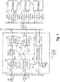
- Fig. 1 depicts an exemplary SPI controller 100, configured to manage communication between the SPI controller 100 (which is an SPI master device and at least one SPI slave device 102 (shown with n SPI slave devices).
- the SPI controller 100 can be coupled to a host computing device via a host bus 104, and the SPI slave devices 102 can be coupled to the SPI controller via an SPI bus 106.
- the terms "host computing device,” “slave device,” “device,” and/or “peripheral device” are meant to be broadly construed to include any type of physical entity that the SPI controller 100 is coupled to.
- peripheral devices using SPIs may include, but are not limited to, various types of sensors (temperature, pressure, etc.) with analog or digital outputs, motor controllers, signal mixers, encoders, potentiometers, power transistors, LCD controllers, accelerometers, CAN controllers, USB controllers, amplifiers, and memory devices, and for chip to chip communications.
- the SPI controller 100 includes a master message processing module 108, a read calibration controller module 110, a Read message processing module 112, a chip select index module 114, and a dynamic clock delay element 116.
- the master message processing module 108, read calibration controller module 110, message processing module 112, and chip select index module 114 can be implemented as hardware, firmware, software, or a combination thereof.
- one or more components of the SPI controller 100 can be implemented using an application specific programmable logic device, such as a field programmable gate array (FPGA), an application-specific integrated circuit (ASIC), a configurable logic block, a microcontroller, a digital signal processor, or the like.
- the embodiments that use hardware and/or firmware can use a hardware description language, such as Very High Speed Integrated Circuit (VHSIC) Hardware Description Language (VHDL) or Verilog.
- VHSIC Very High Speed Integrated Circuit
- VHDL Hardware Description Language
- Verilog Verilog.
- the microcontroller can execute software algorithms, software programs, or code residing on a computer useable medium.
- the SPI controller 100 controls synchronous serial communication with the SPI slave devices 102 so that the SPI controller 100 and electronic devices (not shown) associated with the SPI controller can communicate in a spatially and electronically distributed system with the SPI slave devices 102.
- the SPI controller 100 may be associated with or implemented in a host computing device (not shown), such as a fixed or mobile device, which can be any one or combination of a consumer electronic, communication, navigation, media, computing device, and/or other type of electronic device.
- the SPI controller 100 can be integrated with the host computing device by host bus 104, electronic circuitry, input-output (I/O) logic control, communication interfaces and components, as well as other hardware, firmware, and/or software.
- the slave devices 102 can be implemented in the host computing device or as peripheral devices to the host computing device.
- the SPI controller 100 can include an internal memory 120 and external memory 122
- the internal memory 120 and external memory 122 can include any form of data or information storage means, for example, volatile or non-volatile memory, solid state storage devices, magnetic devices, etc.
- the host computing device can transmit a read request for data from an SPI slave device 102 by transmitting the read request via host bus 104.
- the read request is transmitted from the host bus 104 to the master message processing module 108 via signal line 124.
- the read request includes a chip select index that identifies the SPI slave device from which the data is being requested, and a description of the data requested.
- the master message processing module 108 responds to the read request by requesting the data from the appropriate SPI slave device 102, following SPI protocol, by sending to the SPI bus 106 a SCLK (serial clock) via signal line 126 and Output Data (master-out slave-in (MOSI)) via signal line 128 that includes the description of the data requested.
- the master message processing module 108 further sends the chip select index via signal line 130 to the chip select index module 114.
- the chip select module 114 sends the index via signal line 132 to the SPI bus 106.
- the chip select index module 114 transmits the retrieved phase offset value via signal line 136 to the dynamic clock delay element 116.
- the SPI slave devices 102 receive the SCLK, and MOSI signals via respective signal lines 140 and 142. Only the SPI slave device 102 selected by the chip select index processes the MOSI data and responds by transmitting the requested data (master-in slave-out (MISO)) via signal line 144 to the SPI bus 106.
- the MISO data is transmitted one bit per clock edge of the SCLK signal.
- the MISO is transmitted with an inherent delay. The delay can be caused, for example, by the length of signal lines 138-144, environmental conditions (e.g., temperature), electrical isolation, e.g., across multiple ground planes.
- the delay can be estimated, the actual delay is unknown, unless it is measured. Additionally, the delay can change, such as due to changes to elements that form the SPI bus 106, for example a change to the length of one of signal lines 138-144 or the addition of circuitry. If the delay is not compensated for before providing the requested MISO data to the host bus 104, the data can become misaligned relative to SCLK, causing possible data corruption. In accordance with the disclosure, the delay is compensated for by the dynamic clock delay element 116.
- the chip select index module 114 accesses a data structure 134 using the index to retrieve a phase offset value that is stored in the data structure 134 in association with the index.
- the data structure 134 can be a look-up-table or the like that stores a predefined phase offset value in association with each respective index that identifies the SPI slave devices 1-n.
- the data structure 134 can be stored in internal memory 120 or external memory 122.
- the dynamic clock delay element 116 receives the MISO data via signal line 146.
- the dynamic clock delay element 116 further applies the phase offset value received via signal line 136 to the MISO data to realign the MISO data.
- the realigned MISO data is transmitted via signal line 148 by the dynamic clock delay element 116 to the read message processing module 112.
- the read message processing module 112 transmits the realigned MISO data to the host bus 104, providing the response to the read request.
- the dynamic clock delay element 116 can be implemented using a plurality of delay taps.
- the delay taps and logic for selecting the delay taps can be implemented by one or more of hardware, firmware, or software. If the phase offset value indicates that realignment should be performed, one or more delay taps are selected based on the phase offset value to provide an appropriate phase offset to realign the MISO data.
- FIGS. 2 and 3 shown is a flowchart demonstrating implementation of the various exemplary embodiments. It is noted that the order of steps shown in FIGS. 2 and 3 is not required, so in principle, the various steps may be performed out of the illustrated order. Also certain steps may be skipped, different steps may be added or substituted, or selected steps or groups of steps may be performed in a separate application following the embodiments described herein.
- FIG. 2 is a flowchart showing the operations performed during a read operation.
- a read request is received for described data from an SPI slave device 102 having an index i.
- the data is requested from the indexed SPI slave device 102 using SPI protocol.
- the phase offset value that corresponds to the indexed SPI slave device 102 is determined.
- the requested data is received from the indexed SPI slave device 102.
- the read data received from the indexed SPI slave device 102 is realigned using the phase offset value.
- the realigned read data is processed.
- the processed, realigned read data is sent to the requesting host computing device via the host bus 104.
- the SPI controller 100 can be calibrated to reduce or eliminate leading bit errors and/or trailing bit errors, and to increase the amount of valid read data that is transmitted to the host bus 104.
- a tuning window of phase delay values can be defined by a range that will achieve realignment so that the read data is valid defines a tuning window.
- the center point of the tuning window can be an optimum sampling point for performing calibration.
- the calibration controller module 110 can begin a calibration operation upon the occurrence of an event or satisfaction of a condition, such as at regular time intervals, upon request from the host computing device, in response to a sensor outputting a value that exceeds a threshold value, or upon occurrence of an error condition, such as during processing of the realigned MISO data by the read message processing module 112.
- a calibration operation can be configured to calibrate the phase offset value associated with a selected one or more of the SPI slave devices 102, or to calibrate all of the SPI slave devices 102.
- the calibration controller module 110 can be included with the SPI controller 100 or can be external to the SPI controller 100 and included with the host computing device.
- a user interface module 156 can be provided that permits a user to interact with the calibration controller module 110, such as to initiate a calibration operation and to select which SPI slave devices 102 to calibrate during a calibration operation.
- the user interface module 156 can communicate with the calibration controller module 110 via signal lines 152 and 154.
- the user interface module 156 can be executable by a processor of the host computing device or SPI controller 100.
- the calibration controller module 110 transmits a request for predetermined test data and an index to the master message processing module 108 via signal line 162 for a selected SPI slave device 102 that is to be calibrated during a first iteration.
- the calibration controller module 110 stores original test data that includes the same test pattern used in the predetermined test data requested. Additional iterations will be performed for each SPI slave device 102 that is intended to be calibrated during the calibration operation.
- the master message processing module 108 When the master message processing module 108 receives the request for test data and index, the master message processing module 108 proceeds in a similar fashion to a read operation and transmits the request for test data as MOSI data and SCLK to the SPI bus 106. Additionally, the master message processing module 108 sends the index to the chip select index module 114. The chip select index module 114 then transmits the index to the SPI bus 106. The selected SPI slave device 102 receives the index, SCLK, and request for test data (MOSI signals) and responds by transmitting the requested test data as MISO data via signal line 144 to the SPI bus 106.
- MOSI signals request for test data
- the chip select index 114 consults the data structure 134 to determine the current phase offset value associated with the index and transmits the current phase offset value to the calibration controller module 110 via signal line 164.
- the calibration controller module 110 uses the current phase offset value to select a test offset phase value and provides the test offset phase value to the dynamic clock delay element 116 via signal line 166.
- the dynamic clock delay element 116 receives the requested test data via signal line 146.
- the dynamic clock delay element 116 uses the test phase offset value from the calibration controller module 110 to realign the MISO data.
- the realigned test data is transmitted via signal line 168 by the dynamic clock delay element 116 to the calibration controller module 110.
- the calibration controller module 110 compares the realigned MISO data with the original test data and determines whether the realigned test data is valid, there was a leading bit error, or there was a trailing bit error and generates corresponding test result data. The comparison can be performed serially or in parallel.
- the calibration controller module 110 uses the test result data to iteratively continue calibrating the selected SPI slave device 102 by requesting test data from the selected SPI slave device 102 using different test phase offset values.
- the calibration controller module 110 determines a range of test phase offset values that define a tuning range window for the selected SPI slave device 102.
- the tuning range window includes test phase offset values that cause the realigned MISO data to be valid data, and which are bounded by the test phase offset values that cause occurrences of leading bit errors and trailing bit errors.
- the calibration controller module 110 selects the center point of the tuning range window to be stored in the data structure 134 as the phase offset value associated with the selected SPI slave device 102.
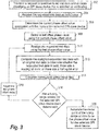
- FIG. 3 is a flowchart showing the operations performed during a calibration operation of a selected SPI slave device 102.
- a request for predetermined test data and an index identifying an SPI slave device 102 that is selected for calibrating is transmitted to the selected SPI slave device 102.
- the requested test data is received as MISO data from the selected SPI device.
- the current phase offset value associated with the index of the selected SPI slave device is determined.
- a test offset phase value is selected using the current phase offset value.
- the requested test data is realigned using the test phase offset value from the calibration controller module 110.
- the realigned requested test data is compared with original test data that corresponds to the predetermined test data to determine whether the requested test data is valid, or there was a leading bit error, or there was a trailing bit error.
- test result data corresponding to the determination of validity/error is generated.
- advantages of some of the embodiments illustrated herein include that multiple SPI slave devices can be associated with different respective phase offset values.
- the phase offset values can be calibrated while the SPI master device (e.g., SPI controller) and SPI slave device are coupled to one another for exchanging messages and even while such messages are being exchanged, e.g., in between messaging processing functions.
- the phase offset value can be calibrated during operation of the SPI master and slave devices, including in real time, in response to conditions such as a sensed change, e.g., a change in temperature, a change in SPI mode, or surpassing a threshold level of allowed read errors.
Landscapes
- Engineering & Computer Science (AREA)
- Theoretical Computer Science (AREA)
- Physics & Mathematics (AREA)
- General Engineering & Computer Science (AREA)
- General Physics & Mathematics (AREA)
- Information Transfer Systems (AREA)
Claims (15)
- Steuerung für eine serielle Peripherieschnittstelle (SPI) zur Verwendung innerhalb eines Computersystems, wobei die SPI-Steuerung Folgendes umfasst:einen Taktgeber, der Systemtaktsignale generiert, die einen Datenübertragungsvorgang synchronisieren;ein dynamisches Taktverzögerungselement (116), das die Taktsignale mit einem Verzögerungsabstand phasenverschiebt und Lesedaten ausgibt, die während eines Lesevorgangs von einer SPI-Slave-Vorrichtung mit den phasenverschobenen Taktsignalen empfangen wurden; dadurch gekennzeichnet, dassdie SPI-Steuerung mit einer Vielzahl von SPI-Slave-Vorrichtungen (102) gekoppelt ist,die SPI-Steuerung ferner eine Datenstruktur umfasst, die einen Index, der die entsprechenden SPI-Slave-Vorrichtungen identifiziert, und einen Verzögerungsabstand speichert, der jedem Index zugeordnet und für die zugeordnete SPI-Slave-Vorrichtung konfiguriert ist.
- SPI-Steuerung nach Anspruch 1, wobei die Verzögerung auf einer Bedingung basierend eingestellt ist.
- SPI-Steuerung nach Anspruch 2, wobei das dynamische Taktverzögerungselement Lesedaten von einer Vielzahl von SPI-Slave-Vorrichtungen während einer Vielzahl von Lesevorgängen empfängt und die Bedingung eine Identifikation der Slave-Vorrichtung ist, von welcher die Lesedaten während des Lesevorgangs empfangen werden.
- SPI-Steuerung nach Anspruch 2, wobei die Bedingung eine Umgebungsbedingung ist.
- SPI-Steuerung nach einem der vorstehenden Ansprüche, ferner eine Kalibrierungssteuerung (110) umfassend, die eine Verzögerung misst, die Lesedaten von der Slave-Vorrichtung zugeordnet ist, und die den Phasenabstand für die Slave-Vorrichtung basierend auf der gemessenen Verzögerung bestimmt.
- SPI-Steuerung nach Anspruch 1, ferner eine Kalibrierungssteuerung umfassend, die die SPI-Steuerung durch Bestimmen einer Übertragungsverzögerung, die der Slave-Vorrichtung zugeordnet ist, kalibriert, wenn die Slave-Vorrichtung ein bekanntes Muster von Lesedaten an die SPI-Steuerung übermittelt, und die Kalibrierungssteuerung der Slave-Vorrichtung basierend auf der bestimmten Verzögerung einen Verzögerungsabstand zuweist.
- SPI-Steuerung nach Anspruch 1, wobei die Kalibrierungssteuerung die SPI-Steuerung kalibriert, während die SPI-Steuerung und SPI-Slave-Vorrichtungen durch Austauschen von Datenübertragung kommunizieren.
- Verfahren zum Lesen von Daten unter Verwendung eines Managementsystems für eine serielle Peripherieschnittstelle (SPI), wobei das Verfahren Folgendes umfasst:Generieren von Systemtaktsignalen, die einen Datenübertragungsvorgang synchronisieren;Phasenverschieben der Taktsignale mit einem Verzögerungsabstand;Ausgeben von Lesedaten, die während eines Lesevorgangs von einer SPI-Slave-Vorrichtung mit den phasenverschobenen Taktsignalen empfangen wurden;dadurch gekennzeichnet, dass es ferner Folgendes umfasst:Koppeln der SPI-Steuerung mit einer Vielzahl von SPI-Slave-Vorrichtungen;Speichern von Indizes, die die entsprechenden SPI-Slave-Vorrichtungen identifizieren; undSpeichern eines Verzögerungsabstandes, der jedem Index zugeordnet ist, wobei der Verzögerungsabstand für die zugeordnete SPI-Slave-Vorrichtung konfiguriert ist.
- Verfahren nach Anspruch 8, das Einstellen der Verzögerung basierend auf einer Bedingung umfassend.
- Verfahren nach Anspruch 9, ferner das Empfangen von Lesedaten von einer Vielzahl von SPI-Slave-Vorrichtungen während einer Vielzahl von Lesevorgängen umfassend, wobei die dem Lesen zugeordnete Bedingung eine Identifikation der Slave-Vorrichtung ist, von welcher die Lesedaten während des Lesevorgangs empfangen werden.
- Verfahren nach Anspruch 9, wobei die Bedingung eine Umgebungsbedingung ist.
- Verfahren nach einem der Ansprüche 8 bis 11, ferner Folgendes umfassend:Bestimmen einer Verzögerung, die Lesedaten zugeordnet ist, die von der Slave-Vorrichtung gelesen wurden; undBestimmen des Phasenabstands für die Slave-Vorrichtung, basierend auf der gemessenen Verzögerung.
- Verfahren nach Anspruch 8, ferner das Kalibrieren der SPI-Steuerung umfassend, Folgendes umfassend:
Bestimmen einer Übertragungsverzögerung, die der Slave-Vorrichtung zugeordnet ist, wenn die Slave-Vorrichtung ein bekanntes Muster von Lesedaten an die SPI-Steuerung übermittelt; und Zuweisen eines Verzögerungsabstands für die Slave-Vorrichtung, basierend auf der bestimmten Verzögerung. - SPI-Steuerung nach Anspruch 1, wobei der Verzögerungsabstand auf einer inhärenten Verzögerung der Übermittlung der Lesedaten basiert.
- Verfahren nach Anspruch 8, wobei der Verzögerungsabstand auf einer inhärenten Verzögerung der Übermittlung der Lesedaten basiert.
Applications Claiming Priority (1)
| Application Number | Priority Date | Filing Date | Title |
|---|---|---|---|
| US14/728,451 US9829913B2 (en) | 2015-06-02 | 2015-06-02 | System and method of realignment of read data by SPI controller |
Publications (2)
| Publication Number | Publication Date |
|---|---|
| EP3101552A1 EP3101552A1 (de) | 2016-12-07 |
| EP3101552B1 true EP3101552B1 (de) | 2019-05-15 |
Family
ID=56098121
Family Applications (1)
| Application Number | Title | Priority Date | Filing Date |
|---|---|---|---|
| EP16172711.0A Active EP3101552B1 (de) | 2015-06-02 | 2016-06-02 | System und verfahren zur neuausrichtung von lesedaten durch spi-steuerung |
Country Status (2)
| Country | Link |
|---|---|
| US (1) | US9829913B2 (de) |
| EP (1) | EP3101552B1 (de) |
Families Citing this family (8)
| Publication number | Priority date | Publication date | Assignee | Title |
|---|---|---|---|---|
| KR102389820B1 (ko) * | 2015-09-22 | 2022-04-22 | 삼성전자주식회사 | 트레이닝 동작을 제어하는 메모리 컨트롤러, 메모리 시스템 및 그의 동작방법 |
| SG11201900499SA (en) * | 2016-07-29 | 2019-02-27 | Razer Asia Pacific Pte Ltd | Interface devices, methods for controlling an interface device, and computer-readable media |
| FR3068797B1 (fr) * | 2017-07-04 | 2019-07-19 | STMicroelectronics (Grand Ouest) SAS | Procede de communication entre un dispositif maitre et n dispositifs esclaves connectes sur un bus de donnees synchrone du type spi et dispositif correspondant |
| US10965442B2 (en) * | 2018-10-02 | 2021-03-30 | Qualcomm Incorporated | Low-power, low-latency time-to-digital-converter-based serial link |
| CN114690849B (zh) * | 2020-12-30 | 2024-06-25 | 华为技术有限公司 | 时钟偏移确定方法、装置及存储介质 |
| CN116303178B (zh) * | 2023-02-28 | 2025-07-25 | 西安思丹德信息技术有限公司 | 一种自适应spi接口装置及自适应时序校准方法 |
| WO2025212910A1 (en) * | 2024-04-03 | 2025-10-09 | Microchip Technology Incorporated | Method and apparatus for training spi controller for high-frequency operation |
| CN119336666B (zh) * | 2024-09-30 | 2025-09-23 | 合肥大唐存储科技有限公司 | 一种串行外设接口的主机接收器 |
Family Cites Families (20)
| Publication number | Priority date | Publication date | Assignee | Title |
|---|---|---|---|---|
| US5627716A (en) | 1990-12-28 | 1997-05-06 | Eaton Corporation | Overcurrent protection device |
| US5572722A (en) * | 1992-05-28 | 1996-11-05 | Texas Instruments Incorporated | Time skewing arrangement for operating random access memory in synchronism with a data processor |
| US6424198B1 (en) | 2001-08-09 | 2002-07-23 | International Business Machines Corporation | Memory clock generation with configurable phase advance and delay capability |
| CA2364506A1 (en) | 2001-12-07 | 2003-06-07 | John W. Bogdan | Integrated timing systems and circuits |
| US6600681B1 (en) * | 2002-06-10 | 2003-07-29 | Lsi Logic Corporation | Method and apparatus for calibrating DQS qualification in a memory controller |
| KR100614638B1 (ko) * | 2003-02-26 | 2006-08-23 | 삼성전자주식회사 | 고속의 무선 통신에 적합한 하이브리드형 직렬 주변 장치 인터페이스 회로 및 그 방법 |
| US8121237B2 (en) * | 2006-03-16 | 2012-02-21 | Rambus Inc. | Signaling system with adaptive timing calibration |
| US20080112255A1 (en) * | 2006-11-15 | 2008-05-15 | Aaron John Nygren | Training of signal transfer channels between memory controller and memory device |
| EP2153525B1 (de) * | 2007-05-29 | 2017-04-05 | Rambus Inc. | Einstellung von taktfehlern an einer schaltkreisschnittstelle |
| US8103936B2 (en) | 2007-10-17 | 2012-01-24 | Micron Technology, Inc. | System and method for data read of a synchronous serial interface NAND |
| DE102009004565B4 (de) | 2009-01-14 | 2015-04-02 | Texas Instruments Deutschland Gmbh | Vorrichtung und Verfahren zum Zwischenspeichern von Daten zwischen Speichercontroller und DRAM |
| US8683164B2 (en) * | 2009-02-04 | 2014-03-25 | Micron Technology, Inc. | Stacked-die memory systems and methods for training stacked-die memory systems |
| US8234422B2 (en) * | 2009-09-11 | 2012-07-31 | Avago Technologies Enterprise IP (Singapore) Pte. Ltd | Interfaces, circuits, and methods for communicating with a double data rate memory device |
| JP5570619B2 (ja) * | 2010-02-23 | 2014-08-13 | ラムバス・インコーポレーテッド | 異なるメモリ種類にアクセスする異なる速度での時分割多重化 |
| US8433838B2 (en) | 2010-09-17 | 2013-04-30 | International Business Machines Corporation | Remote multiplexing devices on a serial peripheral interface bus |
| US9619409B2 (en) * | 2013-01-08 | 2017-04-11 | Taiwan Semiconductor Manufacturing Co., Ltd. | Data sampling alignment method for memory inferface |
| US9813129B2 (en) | 2013-01-28 | 2017-11-07 | Tubis Technology | Hierarchically elaborated phased-array antenna modules and faster beam steering method of operation |
| US8928383B2 (en) | 2013-03-15 | 2015-01-06 | Analog Devices, Inc. | Integrated delayed clock for high speed isolated SPI communication |
| US9361117B2 (en) * | 2014-04-30 | 2016-06-07 | Stmicroelectronics (Grenoble 2) Sas | Tag-based implementations enabling high speed data capture and transparent pre-fetch from a NOR flash |
| KR102333738B1 (ko) * | 2015-02-03 | 2021-12-01 | 삼성전자주식회사 | 불휘발성 메모리 장치 및 불휘발성 메모리 장치의 동작 방법 |
-
2015
- 2015-06-02 US US14/728,451 patent/US9829913B2/en active Active
-
2016
- 2016-06-02 EP EP16172711.0A patent/EP3101552B1/de active Active
Non-Patent Citations (1)
| Title |
|---|
| None * |
Also Published As
| Publication number | Publication date |
|---|---|
| EP3101552A1 (de) | 2016-12-07 |
| US9829913B2 (en) | 2017-11-28 |
| US20160357217A1 (en) | 2016-12-08 |
Similar Documents
| Publication | Publication Date | Title |
|---|---|---|
| EP3101552B1 (de) | System und verfahren zur neuausrichtung von lesedaten durch spi-steuerung | |
| US9275706B2 (en) | Auto-calibration for high speed input/output | |
| US8886988B2 (en) | Method of calibrating signal skews in MIPI and related transmission system | |
| US7246274B2 (en) | Method and apparatus for estimating random jitter (RJ) and deterministic jitter (DJ) from bit error rate (BER) | |
| TW200935236A (en) | Method and apparatus for training the reference voltage level and data sample timing in a receiver | |
| JP7119437B2 (ja) | 車両用マスタ電子制御装置、車両用スレーブ電子制御装置、車両用ログ収集システム及び車両用ログ収集プログラム | |
| JP7189279B2 (ja) | 選択的な遅延クロック信号を用いてバストランザクションを監視することによるセキュリティ保護された通信 | |
| WO2022127815A1 (zh) | 信号采样方法、信号采样装置及计算机可读存储介质 | |
| CN105515893A (zh) | 一种确定采样点位置的方法 | |
| CN109640013B (zh) | 一种时序校准方法及芯片测试机 | |
| CN113115429B (zh) | 一种晶振频偏确定方法、装置及通信系统 | |
| CN115842251B (zh) | 天线采样补偿方法、装置和相控阵平板天线 | |
| CN109213704B (zh) | 用于闪存芯片的信号校准方法及闪存控制器 | |
| US20160254872A1 (en) | Systems and methods for measurement of electrical channel loss | |
| CN111343062B (zh) | 一种车内电子控制单元鉴别方法、系统及存储介质 | |
| CN109167705B (zh) | 获取存储模块内部延时阶梯时间的方法及系统 | |
| CN109359067B (zh) | 获取存储模块内部延时阶梯时间的方法及系统 | |
| US20110060936A1 (en) | Method and apparatus for correction of digitally transmitted information | |
| CN114285509B (zh) | Aau群时延波动补偿方法、装置、电子设备及存储介质 | |
| CN103973299A (zh) | 数据及时钟恢复装置 | |
| TW200303676A (en) | System for providing a calibrated clock and methods thereof | |
| CN114928378A (zh) | 一种单线信号的传输方法、装置及电子设备 | |
| CN121841322A (zh) | 时钟校准电路和时钟校准方法 | |
| JP4462371B2 (ja) | データ受信装置およびマイクロコンピュータ | |
| CN109284239B (zh) | 获取存储模块内部延时阶梯时间的方法及系统 |
Legal Events
| Date | Code | Title | Description |
|---|---|---|---|
| PUAI | Public reference made under article 153(3) epc to a published international application that has entered the european phase |
Free format text: ORIGINAL CODE: 0009012 |
|
| STAA | Information on the status of an ep patent application or granted ep patent |
Free format text: STATUS: THE APPLICATION HAS BEEN PUBLISHED |
|
| AK | Designated contracting states |
Kind code of ref document: A1 Designated state(s): AL AT BE BG CH CY CZ DE DK EE ES FI FR GB GR HR HU IE IS IT LI LT LU LV MC MK MT NL NO PL PT RO RS SE SI SK SM TR |
|
| AX | Request for extension of the european patent |
Extension state: BA ME |
|
| STAA | Information on the status of an ep patent application or granted ep patent |
Free format text: STATUS: REQUEST FOR EXAMINATION WAS MADE |
|
| 17P | Request for examination filed |
Effective date: 20170530 |
|
| RBV | Designated contracting states (corrected) |
Designated state(s): AL AT BE BG CH CY CZ DE DK EE ES FI FR GB GR HR HU IE IS IT LI LT LU LV MC MK MT NL NO PL PT RO RS SE SI SK SM TR |
|
| GRAP | Despatch of communication of intention to grant a patent |
Free format text: ORIGINAL CODE: EPIDOSNIGR1 |
|
| STAA | Information on the status of an ep patent application or granted ep patent |
Free format text: STATUS: GRANT OF PATENT IS INTENDED |
|
| RIC1 | Information provided on ipc code assigned before grant |
Ipc: G06F 13/42 20060101AFI20180607BHEP |
|
| INTG | Intention to grant announced |
Effective date: 20180703 |
|
| GRAJ | Information related to disapproval of communication of intention to grant by the applicant or resumption of examination proceedings by the epo deleted |
Free format text: ORIGINAL CODE: EPIDOSDIGR1 |
|
| STAA | Information on the status of an ep patent application or granted ep patent |
Free format text: STATUS: REQUEST FOR EXAMINATION WAS MADE |
|
| GRAP | Despatch of communication of intention to grant a patent |
Free format text: ORIGINAL CODE: EPIDOSNIGR1 |
|
| STAA | Information on the status of an ep patent application or granted ep patent |
Free format text: STATUS: GRANT OF PATENT IS INTENDED |
|
| INTC | Intention to grant announced (deleted) | ||
| INTG | Intention to grant announced |
Effective date: 20181207 |
|
| GRAS | Grant fee paid |
Free format text: ORIGINAL CODE: EPIDOSNIGR3 |
|
| GRAA | (expected) grant |
Free format text: ORIGINAL CODE: 0009210 |
|
| STAA | Information on the status of an ep patent application or granted ep patent |
Free format text: STATUS: THE PATENT HAS BEEN GRANTED |
|
| AK | Designated contracting states |
Kind code of ref document: B1 Designated state(s): AL AT BE BG CH CY CZ DE DK EE ES FI FR GB GR HR HU IE IS IT LI LT LU LV MC MK MT NL NO PL PT RO RS SE SI SK SM TR |
|
| REG | Reference to a national code |
Ref country code: CH Ref legal event code: EP |
|
| REG | Reference to a national code |
Ref country code: DE Ref legal event code: R096 Ref document number: 602016013874 Country of ref document: DE |
|
| REG | Reference to a national code |
Ref country code: IE Ref legal event code: FG4D |
|
| REG | Reference to a national code |
Ref country code: NL Ref legal event code: MP Effective date: 20190515 |
|
| REG | Reference to a national code |
Ref country code: LT Ref legal event code: MG4D |
|
| PG25 | Lapsed in a contracting state [announced via postgrant information from national office to epo] |
Ref country code: LT Free format text: LAPSE BECAUSE OF FAILURE TO SUBMIT A TRANSLATION OF THE DESCRIPTION OR TO PAY THE FEE WITHIN THE PRESCRIBED TIME-LIMIT Effective date: 20190515 Ref country code: HR Free format text: LAPSE BECAUSE OF FAILURE TO SUBMIT A TRANSLATION OF THE DESCRIPTION OR TO PAY THE FEE WITHIN THE PRESCRIBED TIME-LIMIT Effective date: 20190515 Ref country code: NL Free format text: LAPSE BECAUSE OF FAILURE TO SUBMIT A TRANSLATION OF THE DESCRIPTION OR TO PAY THE FEE WITHIN THE PRESCRIBED TIME-LIMIT Effective date: 20190515 Ref country code: NO Free format text: LAPSE BECAUSE OF FAILURE TO SUBMIT A TRANSLATION OF THE DESCRIPTION OR TO PAY THE FEE WITHIN THE PRESCRIBED TIME-LIMIT Effective date: 20190815 Ref country code: SE Free format text: LAPSE BECAUSE OF FAILURE TO SUBMIT A TRANSLATION OF THE DESCRIPTION OR TO PAY THE FEE WITHIN THE PRESCRIBED TIME-LIMIT Effective date: 20190515 Ref country code: FI Free format text: LAPSE BECAUSE OF FAILURE TO SUBMIT A TRANSLATION OF THE DESCRIPTION OR TO PAY THE FEE WITHIN THE PRESCRIBED TIME-LIMIT Effective date: 20190515 Ref country code: AL Free format text: LAPSE BECAUSE OF FAILURE TO SUBMIT A TRANSLATION OF THE DESCRIPTION OR TO PAY THE FEE WITHIN THE PRESCRIBED TIME-LIMIT Effective date: 20190515 Ref country code: PT Free format text: LAPSE BECAUSE OF FAILURE TO SUBMIT A TRANSLATION OF THE DESCRIPTION OR TO PAY THE FEE WITHIN THE PRESCRIBED TIME-LIMIT Effective date: 20190915 Ref country code: ES Free format text: LAPSE BECAUSE OF FAILURE TO SUBMIT A TRANSLATION OF THE DESCRIPTION OR TO PAY THE FEE WITHIN THE PRESCRIBED TIME-LIMIT Effective date: 20190515 |
|
| PG25 | Lapsed in a contracting state [announced via postgrant information from national office to epo] |
Ref country code: GR Free format text: LAPSE BECAUSE OF FAILURE TO SUBMIT A TRANSLATION OF THE DESCRIPTION OR TO PAY THE FEE WITHIN THE PRESCRIBED TIME-LIMIT Effective date: 20190816 Ref country code: BG Free format text: LAPSE BECAUSE OF FAILURE TO SUBMIT A TRANSLATION OF THE DESCRIPTION OR TO PAY THE FEE WITHIN THE PRESCRIBED TIME-LIMIT Effective date: 20190815 Ref country code: LV Free format text: LAPSE BECAUSE OF FAILURE TO SUBMIT A TRANSLATION OF THE DESCRIPTION OR TO PAY THE FEE WITHIN THE PRESCRIBED TIME-LIMIT Effective date: 20190515 Ref country code: RS Free format text: LAPSE BECAUSE OF FAILURE TO SUBMIT A TRANSLATION OF THE DESCRIPTION OR TO PAY THE FEE WITHIN THE PRESCRIBED TIME-LIMIT Effective date: 20190515 |
|
| REG | Reference to a national code |
Ref country code: AT Ref legal event code: MK05 Ref document number: 1134262 Country of ref document: AT Kind code of ref document: T Effective date: 20190515 |
|
| REG | Reference to a national code |
Ref country code: DE Ref legal event code: R119 Ref document number: 602016013874 Country of ref document: DE |
|
| PG25 | Lapsed in a contracting state [announced via postgrant information from national office to epo] |
Ref country code: EE Free format text: LAPSE BECAUSE OF FAILURE TO SUBMIT A TRANSLATION OF THE DESCRIPTION OR TO PAY THE FEE WITHIN THE PRESCRIBED TIME-LIMIT Effective date: 20190515 Ref country code: DK Free format text: LAPSE BECAUSE OF FAILURE TO SUBMIT A TRANSLATION OF THE DESCRIPTION OR TO PAY THE FEE WITHIN THE PRESCRIBED TIME-LIMIT Effective date: 20190515 Ref country code: AT Free format text: LAPSE BECAUSE OF FAILURE TO SUBMIT A TRANSLATION OF THE DESCRIPTION OR TO PAY THE FEE WITHIN THE PRESCRIBED TIME-LIMIT Effective date: 20190515 Ref country code: CZ Free format text: LAPSE BECAUSE OF FAILURE TO SUBMIT A TRANSLATION OF THE DESCRIPTION OR TO PAY THE FEE WITHIN THE PRESCRIBED TIME-LIMIT Effective date: 20190515 Ref country code: SK Free format text: LAPSE BECAUSE OF FAILURE TO SUBMIT A TRANSLATION OF THE DESCRIPTION OR TO PAY THE FEE WITHIN THE PRESCRIBED TIME-LIMIT Effective date: 20190515 |
|
| REG | Reference to a national code |
Ref country code: CH Ref legal event code: PL |
|
| PG25 | Lapsed in a contracting state [announced via postgrant information from national office to epo] |
Ref country code: SM Free format text: LAPSE BECAUSE OF FAILURE TO SUBMIT A TRANSLATION OF THE DESCRIPTION OR TO PAY THE FEE WITHIN THE PRESCRIBED TIME-LIMIT Effective date: 20190515 Ref country code: IT Free format text: LAPSE BECAUSE OF FAILURE TO SUBMIT A TRANSLATION OF THE DESCRIPTION OR TO PAY THE FEE WITHIN THE PRESCRIBED TIME-LIMIT Effective date: 20190515 Ref country code: MC Free format text: LAPSE BECAUSE OF FAILURE TO SUBMIT A TRANSLATION OF THE DESCRIPTION OR TO PAY THE FEE WITHIN THE PRESCRIBED TIME-LIMIT Effective date: 20190515 |
|
| PLBE | No opposition filed within time limit |
Free format text: ORIGINAL CODE: 0009261 |
|
| STAA | Information on the status of an ep patent application or granted ep patent |
Free format text: STATUS: NO OPPOSITION FILED WITHIN TIME LIMIT |
|
| REG | Reference to a national code |
Ref country code: BE Ref legal event code: MM Effective date: 20190630 |
|
| PG25 | Lapsed in a contracting state [announced via postgrant information from national office to epo] |
Ref country code: TR Free format text: LAPSE BECAUSE OF FAILURE TO SUBMIT A TRANSLATION OF THE DESCRIPTION OR TO PAY THE FEE WITHIN THE PRESCRIBED TIME-LIMIT Effective date: 20190515 |
|
| 26N | No opposition filed |
Effective date: 20200218 |
|
| PG25 | Lapsed in a contracting state [announced via postgrant information from national office to epo] |
Ref country code: PL Free format text: LAPSE BECAUSE OF FAILURE TO SUBMIT A TRANSLATION OF THE DESCRIPTION OR TO PAY THE FEE WITHIN THE PRESCRIBED TIME-LIMIT Effective date: 20190515 Ref country code: DE Free format text: LAPSE BECAUSE OF NON-PAYMENT OF DUE FEES Effective date: 20200101 Ref country code: IE Free format text: LAPSE BECAUSE OF NON-PAYMENT OF DUE FEES Effective date: 20190602 |
|
| PG25 | Lapsed in a contracting state [announced via postgrant information from national office to epo] |
Ref country code: LU Free format text: LAPSE BECAUSE OF NON-PAYMENT OF DUE FEES Effective date: 20190602 Ref country code: SI Free format text: LAPSE BECAUSE OF FAILURE TO SUBMIT A TRANSLATION OF THE DESCRIPTION OR TO PAY THE FEE WITHIN THE PRESCRIBED TIME-LIMIT Effective date: 20190515 Ref country code: BE Free format text: LAPSE BECAUSE OF NON-PAYMENT OF DUE FEES Effective date: 20190630 Ref country code: CH Free format text: LAPSE BECAUSE OF NON-PAYMENT OF DUE FEES Effective date: 20190630 Ref country code: LI Free format text: LAPSE BECAUSE OF NON-PAYMENT OF DUE FEES Effective date: 20190630 |
|
| PG25 | Lapsed in a contracting state [announced via postgrant information from national office to epo] |
Ref country code: RO Free format text: LAPSE BECAUSE OF FAILURE TO SUBMIT A TRANSLATION OF THE DESCRIPTION OR TO PAY THE FEE WITHIN THE PRESCRIBED TIME-LIMIT Effective date: 20190515 |
|
| PG25 | Lapsed in a contracting state [announced via postgrant information from national office to epo] |
Ref country code: CY Free format text: LAPSE BECAUSE OF FAILURE TO SUBMIT A TRANSLATION OF THE DESCRIPTION OR TO PAY THE FEE WITHIN THE PRESCRIBED TIME-LIMIT Effective date: 20190515 |
|
| PG25 | Lapsed in a contracting state [announced via postgrant information from national office to epo] |
Ref country code: IS Free format text: LAPSE BECAUSE OF FAILURE TO SUBMIT A TRANSLATION OF THE DESCRIPTION OR TO PAY THE FEE WITHIN THE PRESCRIBED TIME-LIMIT Effective date: 20190915 |
|
| PG25 | Lapsed in a contracting state [announced via postgrant information from national office to epo] |
Ref country code: MT Free format text: LAPSE BECAUSE OF FAILURE TO SUBMIT A TRANSLATION OF THE DESCRIPTION OR TO PAY THE FEE WITHIN THE PRESCRIBED TIME-LIMIT Effective date: 20190515 Ref country code: HU Free format text: LAPSE BECAUSE OF FAILURE TO SUBMIT A TRANSLATION OF THE DESCRIPTION OR TO PAY THE FEE WITHIN THE PRESCRIBED TIME-LIMIT; INVALID AB INITIO Effective date: 20160602 |
|
| PG25 | Lapsed in a contracting state [announced via postgrant information from national office to epo] |
Ref country code: MK Free format text: LAPSE BECAUSE OF FAILURE TO SUBMIT A TRANSLATION OF THE DESCRIPTION OR TO PAY THE FEE WITHIN THE PRESCRIBED TIME-LIMIT Effective date: 20190515 |
|
| P01 | Opt-out of the competence of the unified patent court (upc) registered |
Effective date: 20230522 |
|
| PGFP | Annual fee paid to national office [announced via postgrant information from national office to epo] |
Ref country code: GB Payment date: 20250520 Year of fee payment: 10 |
|
| PGFP | Annual fee paid to national office [announced via postgrant information from national office to epo] |
Ref country code: FR Payment date: 20250520 Year of fee payment: 10 |