EP3091396B1 - Focusing leveling device - Google Patents
Focusing leveling device Download PDFInfo
- Publication number
- EP3091396B1 EP3091396B1 EP14876090.3A EP14876090A EP3091396B1 EP 3091396 B1 EP3091396 B1 EP 3091396B1 EP 14876090 A EP14876090 A EP 14876090A EP 3091396 B1 EP3091396 B1 EP 3091396B1
- Authority
- EP
- European Patent Office
- Prior art keywords
- sub
- lens group
- beams
- unit
- group
- Prior art date
- Legal status (The legal status is an assumption and is not a legal conclusion. Google has not performed a legal analysis and makes no representation as to the accuracy of the status listed.)
- Active
Links
Images


Classifications
-
- G—PHYSICS
- G03—PHOTOGRAPHY; CINEMATOGRAPHY; ANALOGOUS TECHNIQUES USING WAVES OTHER THAN OPTICAL WAVES; ELECTROGRAPHY; HOLOGRAPHY
- G03F—PHOTOMECHANICAL PRODUCTION OF TEXTURED OR PATTERNED SURFACES, e.g. FOR PRINTING, FOR PROCESSING OF SEMICONDUCTOR DEVICES; MATERIALS THEREFOR; ORIGINALS THEREFOR; APPARATUS SPECIALLY ADAPTED THEREFOR
- G03F9/00—Registration or positioning of originals, masks, frames, photographic sheets or textured or patterned surfaces, e.g. automatically
- G03F9/70—Registration or positioning of originals, masks, frames, photographic sheets or textured or patterned surfaces, e.g. automatically for microlithography
- G03F9/7003—Alignment type or strategy, e.g. leveling, global alignment
- G03F9/7023—Aligning or positioning in direction perpendicular to substrate surface
- G03F9/7026—Focusing
-
- G—PHYSICS
- G03—PHOTOGRAPHY; CINEMATOGRAPHY; ANALOGOUS TECHNIQUES USING WAVES OTHER THAN OPTICAL WAVES; ELECTROGRAPHY; HOLOGRAPHY
- G03F—PHOTOMECHANICAL PRODUCTION OF TEXTURED OR PATTERNED SURFACES, e.g. FOR PRINTING, FOR PROCESSING OF SEMICONDUCTOR DEVICES; MATERIALS THEREFOR; ORIGINALS THEREFOR; APPARATUS SPECIALLY ADAPTED THEREFOR
- G03F7/00—Photomechanical, e.g. photolithographic, production of textured or patterned surfaces, e.g. printing surfaces; Materials therefor, e.g. comprising photoresists; Apparatus specially adapted therefor
- G03F7/70—Microphotolithographic exposure; Apparatus therefor
- G03F7/70058—Mask illumination systems
- G03F7/70141—Illumination system adjustment, e.g. adjustments during exposure or alignment during assembly of illumination system
-
- G—PHYSICS
- G03—PHOTOGRAPHY; CINEMATOGRAPHY; ANALOGOUS TECHNIQUES USING WAVES OTHER THAN OPTICAL WAVES; ELECTROGRAPHY; HOLOGRAPHY
- G03F—PHOTOMECHANICAL PRODUCTION OF TEXTURED OR PATTERNED SURFACES, e.g. FOR PRINTING, FOR PROCESSING OF SEMICONDUCTOR DEVICES; MATERIALS THEREFOR; ORIGINALS THEREFOR; APPARATUS SPECIALLY ADAPTED THEREFOR
- G03F7/00—Photomechanical, e.g. photolithographic, production of textured or patterned surfaces, e.g. printing surfaces; Materials therefor, e.g. comprising photoresists; Apparatus specially adapted therefor
- G03F7/70—Microphotolithographic exposure; Apparatus therefor
- G03F7/70216—Mask projection systems
- G03F7/70275—Multiple projection paths, e.g. array of projection systems, microlens projection systems or tandem projection systems
-
- G—PHYSICS
- G03—PHOTOGRAPHY; CINEMATOGRAPHY; ANALOGOUS TECHNIQUES USING WAVES OTHER THAN OPTICAL WAVES; ELECTROGRAPHY; HOLOGRAPHY
- G03F—PHOTOMECHANICAL PRODUCTION OF TEXTURED OR PATTERNED SURFACES, e.g. FOR PRINTING, FOR PROCESSING OF SEMICONDUCTOR DEVICES; MATERIALS THEREFOR; ORIGINALS THEREFOR; APPARATUS SPECIALLY ADAPTED THEREFOR
- G03F7/00—Photomechanical, e.g. photolithographic, production of textured or patterned surfaces, e.g. printing surfaces; Materials therefor, e.g. comprising photoresists; Apparatus specially adapted therefor
- G03F7/70—Microphotolithographic exposure; Apparatus therefor
- G03F7/70483—Information management; Active and passive control; Testing; Wafer monitoring, e.g. pattern monitoring
- G03F7/70605—Workpiece metrology
- G03F7/70616—Monitoring the printed patterns
- G03F7/70641—Focus
-
- G—PHYSICS
- G03—PHOTOGRAPHY; CINEMATOGRAPHY; ANALOGOUS TECHNIQUES USING WAVES OTHER THAN OPTICAL WAVES; ELECTROGRAPHY; HOLOGRAPHY
- G03F—PHOTOMECHANICAL PRODUCTION OF TEXTURED OR PATTERNED SURFACES, e.g. FOR PRINTING, FOR PROCESSING OF SEMICONDUCTOR DEVICES; MATERIALS THEREFOR; ORIGINALS THEREFOR; APPARATUS SPECIALLY ADAPTED THEREFOR
- G03F7/00—Photomechanical, e.g. photolithographic, production of textured or patterned surfaces, e.g. printing surfaces; Materials therefor, e.g. comprising photoresists; Apparatus specially adapted therefor
- G03F7/70—Microphotolithographic exposure; Apparatus therefor
- G03F7/70483—Information management; Active and passive control; Testing; Wafer monitoring, e.g. pattern monitoring
- G03F7/70605—Workpiece metrology
- G03F7/70681—Metrology strategies
- G03F7/70683—Mark designs
-
- G—PHYSICS
- G03—PHOTOGRAPHY; CINEMATOGRAPHY; ANALOGOUS TECHNIQUES USING WAVES OTHER THAN OPTICAL WAVES; ELECTROGRAPHY; HOLOGRAPHY
- G03F—PHOTOMECHANICAL PRODUCTION OF TEXTURED OR PATTERNED SURFACES, e.g. FOR PRINTING, FOR PROCESSING OF SEMICONDUCTOR DEVICES; MATERIALS THEREFOR; ORIGINALS THEREFOR; APPARATUS SPECIALLY ADAPTED THEREFOR
- G03F7/00—Photomechanical, e.g. photolithographic, production of textured or patterned surfaces, e.g. printing surfaces; Materials therefor, e.g. comprising photoresists; Apparatus specially adapted therefor
- G03F7/70—Microphotolithographic exposure; Apparatus therefor
- G03F7/70483—Information management; Active and passive control; Testing; Wafer monitoring, e.g. pattern monitoring
- G03F7/70605—Workpiece metrology
- G03F7/706843—Metrology apparatus
- G03F7/706849—Irradiation branch, e.g. optical system details, illumination mode or polarisation control
-
- G—PHYSICS
- G03—PHOTOGRAPHY; CINEMATOGRAPHY; ANALOGOUS TECHNIQUES USING WAVES OTHER THAN OPTICAL WAVES; ELECTROGRAPHY; HOLOGRAPHY
- G03F—PHOTOMECHANICAL PRODUCTION OF TEXTURED OR PATTERNED SURFACES, e.g. FOR PRINTING, FOR PROCESSING OF SEMICONDUCTOR DEVICES; MATERIALS THEREFOR; ORIGINALS THEREFOR; APPARATUS SPECIALLY ADAPTED THEREFOR
- G03F7/00—Photomechanical, e.g. photolithographic, production of textured or patterned surfaces, e.g. printing surfaces; Materials therefor, e.g. comprising photoresists; Apparatus specially adapted therefor
- G03F7/70—Microphotolithographic exposure; Apparatus therefor
- G03F7/70483—Information management; Active and passive control; Testing; Wafer monitoring, e.g. pattern monitoring
- G03F7/70605—Workpiece metrology
- G03F7/706843—Metrology apparatus
- G03F7/706851—Detection branch, e.g. detector arrangements, polarisation control, wavelength control or dark/bright field detection
-
- G—PHYSICS
- G03—PHOTOGRAPHY; CINEMATOGRAPHY; ANALOGOUS TECHNIQUES USING WAVES OTHER THAN OPTICAL WAVES; ELECTROGRAPHY; HOLOGRAPHY
- G03F—PHOTOMECHANICAL PRODUCTION OF TEXTURED OR PATTERNED SURFACES, e.g. FOR PRINTING, FOR PROCESSING OF SEMICONDUCTOR DEVICES; MATERIALS THEREFOR; ORIGINALS THEREFOR; APPARATUS SPECIALLY ADAPTED THEREFOR
- G03F9/00—Registration or positioning of originals, masks, frames, photographic sheets or textured or patterned surfaces, e.g. automatically
- G03F9/70—Registration or positioning of originals, masks, frames, photographic sheets or textured or patterned surfaces, e.g. automatically for microlithography
- G03F9/7003—Alignment type or strategy, e.g. leveling, global alignment
- G03F9/7023—Aligning or positioning in direction perpendicular to substrate surface
- G03F9/7034—Leveling
-
- G—PHYSICS
- G03—PHOTOGRAPHY; CINEMATOGRAPHY; ANALOGOUS TECHNIQUES USING WAVES OTHER THAN OPTICAL WAVES; ELECTROGRAPHY; HOLOGRAPHY
- G03F—PHOTOMECHANICAL PRODUCTION OF TEXTURED OR PATTERNED SURFACES, e.g. FOR PRINTING, FOR PROCESSING OF SEMICONDUCTOR DEVICES; MATERIALS THEREFOR; ORIGINALS THEREFOR; APPARATUS SPECIALLY ADAPTED THEREFOR
- G03F9/00—Registration or positioning of originals, masks, frames, photographic sheets or textured or patterned surfaces, e.g. automatically
- G03F9/70—Registration or positioning of originals, masks, frames, photographic sheets or textured or patterned surfaces, e.g. automatically for microlithography
- G03F9/7065—Production of alignment light, e.g. light source, control of coherence, polarization, pulse length, wavelength
Definitions
- the present invention relates to photolithography and, more particularly, to an apparatus having a refractive unit for automatic focusing and leveling in a photolithography tool.
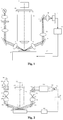
- FIG. 1 is a schematic illustration of such a focusing and leveling system used in a conventional projection photolithography tool.
- the focusing and leveling system includes a projection objective 19 and an optical measuring path extending on both sides of an optical axis of the projection objective 19.
- Disposed in the optical measuring path are an illuminating unit, a projecting unit, a detecting unit and a relay lens group arranged in this order.
- the illuminating unit is composed of an illumination light source 1, an illumination lens group 2 and fiber optics (not shown).
- the projecting unit is composed of projection slits 3, an upstream projection lens group 4, a reflector group 5 and a downstream projection lens group 6.
- Light exiting the illuminating unit passes sequentially through the projection slits 3, the upstream projection lens group 4, the reflector group 5 and the downstream projection lens group 6, and then forms light spots to be measured in an exposure area on the surface of the object 7 being measured.
- the detecting unit is composed of an upstream detection lens group 8, a reflector group 9 and a downstream detection lens group 10.
- the relaying unit is disposed downstream relative to the detecting unit and is made up of a relay reflector 11, a relay lens group 12, a detector 13, a focusing controller 14 and an arithmetic unit 15.
- a relay reflector 11 When travelling in the relaying unit, light forming the spots is received by the detector 13 and converted thereby to a light intensity signal indicative of the position and tilt of the surface of the object being measured.
- the U.S. Patent No. US5414515 provides a device with a single optical path and multiple light spots, in which, in order to achieve a measurement field of view having a required size, a plurality of charge-coupled devices (CCDs) is used.
- CCDs charge-coupled devices
- US6080990 discloses a position measuring apparatus comprising a detection unit with a refractive unit in order to configure the detected light beams in a linear array.
- a focusing and leveling apparatus includes: an illumination light source for emanating a light beam; and an illumination lens group, a projecting unit, an object being measured, a detecting unit, a refractive unit, a relay lens group and a photoelectric detector, disposed sequentially in this order in a transmission path of the light beam.
- the photoelectric detector is configured to convert the light beam that has exited the relay lens group and carries information about a level and a tilt of the surface of the object being measured to an electrical signal and pass the electrical signal on to an arithmetic unit and a focusing and leveling controller.
- the arithmetic unit is configured to produce a control signal for the focusing and leveling controller based on the received electrical signal such that the focusing and leveling controller controls a wafer stage that supports the object being measured so as to adjust the level and tilt of the surface of the object being measured.
- the projecting unit includes projection slits defining a plurality of non-linearly arranged marks, such that after passing sequentially through the illumination lens group, the projecting unit, the object being measured and the detecting unit, the light beam emanated by the illumination light source becomes a plurality of non-linearly arranged sub-beams corresponding to the plurality of marks.
- the refractive unit is so configured that after passing through the refractive unit, the plurality of sub-beams form a plurality of linearly arranged light spots.
- the projection slits define at least three non-linearly arranged marks.
- the projecting unit further comprises a double-prism group having two prisms sandwiching the projection slits therebetween.
- the refractive unit comprises a reflector group, a lens group and a prism group.
- the reflector group consists of n-1 pairs of reflectors
- the lens group consists of n lenses
- the prism group consists of n-1 prisms, where n corresponds to the number of the non-linearly arranged marks defined by the projection slits.
- the refractive unit further includes a parallel-sided plate, wherein a middle one of the plurality of sub-beams incident on the refractive unit passes through a corresponding one of the lenses and is then incident on the parallel-sided plate, with the remaining ones of the plurality of sub-beams traveling sequentially through corresponding pairs of the reflectors, corresponding ones of the lenses and prisms and then being incident, together with the middle sub-beam, on the relay lens group.
- the photoelectric detector is a single CCD linear array .
- the refractive unit includes two wedges disposed with their sloped faces facing each other.
- a first one of the two wedges defines first through-holes in its middle and lower parts at locations corresponding to incidence of the middle and lower ones of the plurality of sub-beams on the first wedge of the refractive unit
- a second one of the two wedges defines second through-holes in its middle and upper parts at locations corresponding to incidence of the middle and upper ones of the plurality of sub-beams on the second wedge of the refractive unit.
- the refractive unit further includes a parallel-sided plate so disposed that the middle one of the plurality of sub-beams passes through the first and second through-holes defined in the respective middle parts of the first and second wedges and is then incident on the parallel-sided plate.
- the present invention provides a novel structure for focusing and leveling sub-systems in projection photolithography tools, in which a refractive unit is introduced in an optical path, thereby satisfying the system requirements for a large field of view and multipoint measurement with a single optical path and a single CCD linear array and resulting in overall reductions in cost and footprint.
- FIG. 2 schematically shows a focusing and leveling apparatus having a refractive unit for use in a projection photolithography tool according to the present invention.
- the apparatus comprises an illumination light source 101, an illumination lens group 102, projection slits 103, a double-prism group 104, an upstream projection lens group 105, a projection diaphragm 106, a downstream projection lens group 107, a projection reflector 108, an object 109 being measured, an upstream detection reflector 110, an upstream detection lens group 111, a detection diaphragm 112, a downstream detection lens group 113, a downstream detection reflector 114, a refractive unit 115, a relay lens group 116, a CCD linear array 117, a focusing controller 118, and an arithmetic unit 119.
- a light beam from the illumination light source 101 passes through the illumination lens group 102 and is then incident on the projection slits 103 which is sandwiched between the two prisms of the double-prism group 104.
- sub-beams are generated and travel through the upstream projection lens group 105, the projection diaphragm 106 and the downstream projection lens group 107, and are then reflected by the projection reflector 108 onto the object 109.
- the object 109 then reflects the sub-beams onto the upstream detection reflector 110, which, in turn, reflects the sub-beams into the upstream detection lens group 111.
- the sub-beams After traveling through the upstream detection lens group 111, the sub-beams further propagate through the detection diaphragm 112 and the downstream detection lens group 113, and are then reflected by the downstream detection reflector 114 into the refractive unit 115. Upon exiting the refractive unit 115, the sub-beams form light spots distributed in a single linear field of view, and then further transmit through the relay lens group 116 and are received by the CCD linear array 117, where the light is subjected to photoelectric conversion and thereby results in a signal indicative of information about a level and a tilt of the surface of the object being measured. The signal is then passed by the focusing controller 118 on to the arithmetic unit 119, where the signal is processed to perform control over a wafer stage 120 such that the object 109 is adjusted in its surface level and tilt as desired.
- FIG. 3 shows a focusing and leveling apparatus having a refractive unit for use in a focusing and leveling sub-system of a projection photolithography tool, constructed in accordance with Embodiment 1 of the present invention.
- the apparatus is used for accurate and efficient measurement of the position of a wafer surface.
- the apparatus comprises an illumination light source 201, an illumination lens group 202, projection slits 203, a double-prism group 204, an upstream projection lens group 205, a projection diaphragm 206, a downstream projection lens group 207, a projection reflector 208, an object 209 being measured, an upstream detection reflector 210, an upstream detection lens group 211, a detection diaphragm 212, a downstream detection lens group 213, a downstream detection reflector 214, a reflector group 215 of the refractive unit, a lens group 216 of the refractive unit, a parallel-sided plate 217, a prism group 218 of the refractive unit, a relay lens group 219, a CCD linear array 220, a focusing controller 221 and an arithmetic unit 222.
- a light beam from the illumination light source 201 passes through the illumination lens group 202 and is then incident on the projection slits 203 which is sandwiched between the two prisms of the double-prism group 204.
- sub-beams are generated and travel through the upstream projection lens group 205, the projection diaphragm 206 and the downstream projection lens group 207, and are then reflected by the projection reflector 208 onto the object 209.
- the object 209 then reflects the sub-beams onto the upstream detection reflector 210, which, in turn, reflects the sub-beams into the upstream detection lens group 211.
- the sub-beams After traveling through the upstream detection lens group 211, the sub-beams further propagate through the detection diaphragm 212 and the downstream detection lens group 213, and are then reflected by the downstream detection reflector 214 onto the reflector group 215 (i.e., reflectors 215a-215h).
- the sub-beams After leaving the reflector group 215, the sub-beams travel through the lens group 216 (i.e., respectively through lens 216a-216e), and then a middle one of the sub-beams passes through the parallel-sided plate 217, with all the rest, peripheral ones of the sub-beams passing through the prism group 218 (i.e., respectively through prisms 218a-218d), wherein mark B corresponds to 215a, 215b, 216a and 218a, mark A to 215c, 215d, 216b and 218b, mark D to 215e, 215f, 216c and 218c, and mark E to 215g, 215h, 216d and 218d.
- mark B corresponds to 215a, 215b, 216a and 218a
- mark A to 215c, 215d, 216b and 218b mark D to 215e, 215f, 216c and 218c
- mark E to 215
- all the sub-beams transmit through the relay lens group 219 and are received by the CCD linear array 220, where they are subjected to photoelectric conversion and result in information about a level and a tilt of the surface of the object being measured.
- the information is then transferred by the focusing controller 221 to the arithmetic unit 222, in order to perform control over a wafer stage 223 such that the object 209 is adjusted in its surface level and tilt as desired.
- the sub-beams have been illustrated as being incident on the refractive unit in a horizontal orientation in this embodiment, the present invention is not limited to such horizontal incidence in practical applications.
- FIG. 4 is a partial view of the refractive unit having the reflectors. As shown in the figure, the refractive unit includes the reflector group 215, the lens group 216, the parallel-sided plate 217 and the prism group 218. After the sub-beams are reflected by the reflector group 215, they are incident on and travel through the lens group 216.
- the middle one of the sub-beams Upon exiting the lens group 216, the middle one of the sub-beams transmits through the parallel-sided plate 217, and the remaining four peripheral sub-beams all pass through the prism group 218. Thereafter, the peripheral sub-beams, together with the middle sub-beam, pass through the relay lens group 219 and are received by the CCD linear array 220.
- FIGs. 5A and 6A show two applicable layouts of the projection slits.
- the slits are disposed between the two prisms of the double-prism group 204 in a tilted configuration, and the marks A, B, C, D and E of the projection slits are arranged at the locations indicated in the respective figure.
- FIGs. 5B and 6B show spatially distributed light spots A', B', C', D' and E' formed on an image plane before the sub-beams pass through the refractive unit in cases of the respective layouts of the projection slits being used.
- 5C and 6C show linearly distributed light spots A", B", C", D" and E" formed on an image plane after the sub-beams have passed through the refractive unit in cases of the respective layouts of the projection slits being used.
- the sub-beams finally travel through the relay lens group 219 and are received by the CCD linear array 220, thereby converting the planar distribution of the light spots in the field of view to a desired linear distribution.
- FIG. 7 shows light spots formed by the sub-beams on the CCD linear array in both of the cases shown in FIGs. 5C and 6C , wherein the light spots appear as linearly arranged patterns A"', B"', C"', D"' and E"'.
- FIG. 8 is a schematic illustration of a focusing and leveling apparatus having a refractive unit with a wedge group for use in a focusing and leveling sub-system of a projection photolithography tool, constructed in accordance with Embodiment 2 of the present invention.
- the apparatus is used for accurate and efficient measurement of the position of a wafer surface.
- the apparatus comprises an illumination light source 301, an illumination lens group 302, projection slits 303, a double-prism group 304, an upstream projection lens group 305, a projection diaphragm 306, a downstream projection lens group 307, a projection reflector 308, an object 309 being measured, an upstream detection reflector 310, an upstream detection lens group 311, a detection diaphragm 312, a downstream detection lens group 313, a downstream detection reflector 314, a wedge group 315 of the refractive unit, a parallel-sided plate 316, a relay lens group 317, a CCD linear array 318, a focusing controller 319 and an arithmetic unit 320.
- a light beam from the illumination light source 301 passes through the illumination lens group 302 and is then incident on the projection slits 303 which is sandwiched between the two prisms of the double-prism group 304.
- sub-beams are generated and travel through the upstream projection lens group 305, the projection diaphragm 306 and the downstream projection lens group 307, and are reflected by the projection reflector 308 onto the object 309.
- the object 309 subsequently reflects the sub-beams onto the upstream detection reflector 310, which, in turn, reflects the sub-beams into the upstream detection lens group 311.
- the sub-beams After traveling through the upstream detection lens group 311, the sub-beams further propagate through the detection diaphragm 312 and the downstream detection lens group 313, and are then reflected by the downstream detection reflector 314 into the wedge group 315.
- a middle one of the sub-beams After exiting the wedge group 315, a middle one of the sub-beams passes through the parallel-sided plate 316, and then, together with the rest, peripheral ones of the sub-beams, transmits through the relay lens group 317 and is received by the CCD linear array 318, where the sub-beams are subjected to photoelectric conversion and result in information about a level and a tilt of the surface of the object being measured.
- the information is then transferred by the focusing controller 319 to the arithmetic unit 320, in order to perform control over a wafer stage 321 such that the object 309 is adjusted in its surface level and tilt as desired.
- FIG. 9 is a schematic illustration of the refractive unit having the wedge group.
- the refractive unit includes the parallel-sided plate 316 and the wedge group 315.
- the wedge group 315 is composed of two wedges disposed with their sharp corners opposite to each other. After being reflected by the downstream detection reflector 314, the sub-beams are imaged on a single image plane by the two wedges 315.
- the wedge 315a is disposed with its sharp corner oriented in the same direction as the orientation of the marks B and D (i.e., upward), and the sharp corner of the wedge 315b is oriented in the same direction as the orientation of the marks A and E (i.e., downward).
- the sub-beams are incident on a face of the upstream wedge 315a at an angle that is desired to be as near to 90° as possible, and is finally imaged on the CCD linear array 318 by the relay lens group 317.
- the wedge 315a defines two holes at locations corresponding to the incidence of the lower two of the aforementioned sub-beams, while the wedge 315b defines two holes at locations corresponding to the incidence of the upper two of the sub-beams that have been deflected by the wedge 315a.
- each of the wedges 315a and 315b further defines a hole corresponding to the incidence of a middle one of the sub-beams. All of these holes are through-holes without deflecting the sub-beams during their passage therethrough.
- the parallel-sided plate 316 is disposed to compensate for an optical path difference of the middle sub-beams, such that the planar distribution of the light spots is converted to a desired distribution after the sub-beams have passed through the wedge group 315, and the sub-beams then transmit through the relay lens group 317 and are finally received by the CCD linear array 320.
Landscapes
- Physics & Mathematics (AREA)
- General Physics & Mathematics (AREA)
- Exposure And Positioning Against Photoresist Photosensitive Materials (AREA)
- Exposure Of Semiconductors, Excluding Electron Or Ion Beam Exposure (AREA)
- Automatic Focus Adjustment (AREA)
Description
- The present invention relates to photolithography and, more particularly, to an apparatus having a refractive unit for automatic focusing and leveling in a photolithography tool.
- Current projection photolithography systems typically include an automatic focusing and leveling sub-system for accurately measuring a level and a tilt of the surface of an object.
FIG. 1 is a schematic illustration of such a focusing and leveling system used in a conventional projection photolithography tool. As shown inFIG. 1 , the focusing and leveling system includes aprojection objective 19 and an optical measuring path extending on both sides of an optical axis of theprojection objective 19. Disposed in the optical measuring path are an illuminating unit, a projecting unit, a detecting unit and a relay lens group arranged in this order. The illuminating unit is composed of an illumination light source 1, an illumination lens group 2 and fiber optics (not shown). Light emanated from the light source 1 is condensed by the illumination lens group 2 and directed through the fiber optics onto the projecting unit, thereby providing illuminating light to the whole measuring system. The projecting unit is composed of projection slits 3, an upstream projection lens group 4, areflector group 5 and a downstream projection lens group 6. Light exiting the illuminating unit passes sequentially through the projection slits 3, the upstream projection lens group 4, thereflector group 5 and the downstream projection lens group 6, and then forms light spots to be measured in an exposure area on the surface of theobject 7 being measured. The detecting unit is composed of an upstreamdetection lens group 8, a reflector group 9 and a downstreamdetection lens group 10. The relaying unit is disposed downstream relative to the detecting unit and is made up of a relay reflector 11, arelay lens group 12, adetector 13, a focusingcontroller 14 and anarithmetic unit 15. When travelling in the relaying unit, light forming the spots is received by thedetector 13 and converted thereby to a light intensity signal indicative of the position and tilt of the surface of the object being measured. - As disclosed in one of its embodiments, the
U.S. Patent No. US5414515 provides a device with a single optical path and multiple light spots, in which, in order to achieve a measurement field of view having a required size, a plurality of charge-coupled devices (CCDs) is used. This design is disadvantageous in that the use of multiple CCDs, as wells as, corresponding image capture cards and cables, leads to high cost and increased footprint constraints on the whole photolithography tool in which the device is employed. - A similar focussing and levelling apparatus is disclosed in
EP1349011 . - It is an objective of the present invention to provide a novel structure for focusing and leveling sub-systems in projection photolithography tools, in which a refractive unit is introduced in an optical path, thereby satisfying the system requirements for a large field of view and multipoint measurement with a single optical path and a single CCD linear array and resulting in overall reductions in cost and footprint.
-
US6080990 discloses a position measuring apparatus comprising a detection unit with a refractive unit in order to configure the detected light beams in a linear array. A focusing and leveling apparatus according to the present invention includes: an illumination light source for emanating a light beam; and an illumination lens group, a projecting unit, an object being measured, a detecting unit, a refractive unit, a relay lens group and a photoelectric detector, disposed sequentially in this order in a transmission path of the light beam. The photoelectric detector is configured to convert the light beam that has exited the relay lens group and carries information about a level and a tilt of the surface of the object being measured to an electrical signal and pass the electrical signal on to an arithmetic unit and a focusing and leveling controller. The arithmetic unit is configured to produce a control signal for the focusing and leveling controller based on the received electrical signal such that the focusing and leveling controller controls a wafer stage that supports the object being measured so as to adjust the level and tilt of the surface of the object being measured. The projecting unit includes projection slits defining a plurality of non-linearly arranged marks, such that after passing sequentially through the illumination lens group, the projecting unit, the object being measured and the detecting unit, the light beam emanated by the illumination light source becomes a plurality of non-linearly arranged sub-beams corresponding to the plurality of marks. The refractive unit is so configured that after passing through the refractive unit, the plurality of sub-beams form a plurality of linearly arranged light spots. - Preferably, the projection slits define at least three non-linearly arranged marks.
- Preferably, the projecting unit further comprises a double-prism group having two prisms sandwiching the projection slits therebetween.
- Preferably, the refractive unit comprises a reflector group, a lens group and a prism group.
- Preferably, the reflector group consists of n-1 pairs of reflectors, the lens group consists of n lenses, and the prism group consists of n-1 prisms, where n corresponds to the number of the non-linearly arranged marks defined by the projection slits.
- Preferably, the refractive unit further includes a parallel-sided plate, wherein a middle one of the plurality of sub-beams incident on the refractive unit passes through a corresponding one of the lenses and is then incident on the parallel-sided plate, with the remaining ones of the plurality of sub-beams traveling sequentially through corresponding pairs of the reflectors, corresponding ones of the lenses and prisms and then being incident, together with the middle sub-beam, on the relay lens group.
- Preferably, the photoelectric detector is a single CCD linear array .
- Preferably, the refractive unit includes two wedges disposed with their sloped faces facing each other.
- Preferably, a first one of the two wedges defines first through-holes in its middle and lower parts at locations corresponding to incidence of the middle and lower ones of the plurality of sub-beams on the first wedge of the refractive unit, and a second one of the two wedges defines second through-holes in its middle and upper parts at locations corresponding to incidence of the middle and upper ones of the plurality of sub-beams on the second wedge of the refractive unit.
- Preferably, the refractive unit further includes a parallel-sided plate so disposed that the middle one of the plurality of sub-beams passes through the first and second through-holes defined in the respective middle parts of the first and second wedges and is then incident on the parallel-sided plate.
- Differing from the two schemes commonly adopted in the prior art, i.e., a first scheme having multiple optical paths and producing multiple light spots to be measured, in which a plurality of CCD linear arrays are used to meet the requirement for a large measurement field of view, and a second scheme having a single optical path and producing multiple light spots to be measured, in which a single CCD planar array is used to achieve a large measurement field of view, the present invention provides a novel structure for focusing and leveling sub-systems in projection photolithography tools, in which a refractive unit is introduced in an optical path, thereby satisfying the system requirements for a large field of view and multipoint measurement with a single optical path and a single CCD linear array and resulting in overall reductions in cost and footprint.
- The advantages and spirit of the invention will be better understood from the following detailed description when considered with reference to the accompanying drawings, in which:
-
FIG. 1 is a schematic illustration of a focusing and leveling system of a projection photolithography tool; -
FIG. 2 schematically illustrates a focusing and leveling system having a refractive unit according to the present invention; -
FIG. 3 schematically shows a focusing and leveling apparatus having a refractive unit with a reflector group according to the present invention; -
FIG. 4 is a partial view of the refractive unit with a reflector group according to the present invention; -
FIG. 5A is a schematic illustrating projection slits in accordance with an embodiment of the present invention; -
FIG. 5B shows locations on an image plane where light spots are formed before a light beam passes through the refractive unit in accordance with an embodiment of the present invention; -
FIG. 5C shows locations on an image plane where light spots are formed after a light beam has passed through the refractive unit in accordance with an embodiment of the present invention; -
FIG. 6A is a schematic illustrating projection slits in accordance with another embodiment of the present invention; -
FIG. 5B shows locations on an image plane where light spots are formed before a light beam passes through the refractive unit in accordance with another embodiment of the present invention; -
FIG. 5C shows locations on an image plane where light spots are formed after a light beam has passed through the refractive unit in accordance with another embodiment of the present invention; -
FIG. 7 shows locations on a CCD linear array where light spots are formed by the light beams ofFIGs. 5C and 6C ; -
FIG. 8 is a schematic illustrating a focusing and leveling apparatus having a refractive unit with a wedge group according to the present invention; and -
FIG. 9 is a partial view of the refractive unit with a wedge group according to the present invention. - Some specific Embodiments of the present invention will be described below with reference to the accompanying drawings.
-
FIG. 2 schematically shows a focusing and leveling apparatus having a refractive unit for use in a projection photolithography tool according to the present invention. As illustrated, the apparatus comprises anillumination light source 101, anillumination lens group 102,projection slits 103, a double-prism group 104, an upstream projection lens group 105, aprojection diaphragm 106, a downstreamprojection lens group 107, aprojection reflector 108, anobject 109 being measured, anupstream detection reflector 110, an upstreamdetection lens group 111, adetection diaphragm 112, a downstreamdetection lens group 113, adownstream detection reflector 114, arefractive unit 115, arelay lens group 116, a CCDlinear array 117, a focusingcontroller 118, and anarithmetic unit 119. A light beam from theillumination light source 101 passes through theillumination lens group 102 and is then incident on theprojection slits 103 which is sandwiched between the two prisms of the double-prism group 104. After exiting the double-prism group 104, sub-beams are generated and travel through the upstream projection lens group 105, theprojection diaphragm 106 and the downstreamprojection lens group 107, and are then reflected by theprojection reflector 108 onto theobject 109. Theobject 109 then reflects the sub-beams onto theupstream detection reflector 110, which, in turn, reflects the sub-beams into the upstreamdetection lens group 111. After traveling through the upstreamdetection lens group 111, the sub-beams further propagate through thedetection diaphragm 112 and the downstreamdetection lens group 113, and are then reflected by thedownstream detection reflector 114 into therefractive unit 115. Upon exiting therefractive unit 115, the sub-beams form light spots distributed in a single linear field of view, and then further transmit through therelay lens group 116 and are received by the CCDlinear array 117, where the light is subjected to photoelectric conversion and thereby results in a signal indicative of information about a level and a tilt of the surface of the object being measured. The signal is then passed by the focusingcontroller 118 on to thearithmetic unit 119, where the signal is processed to perform control over awafer stage 120 such that theobject 109 is adjusted in its surface level and tilt as desired. -
FIG. 3 shows a focusing and leveling apparatus having a refractive unit for use in a focusing and leveling sub-system of a projection photolithography tool, constructed in accordance with Embodiment 1 of the present invention. The apparatus is used for accurate and efficient measurement of the position of a wafer surface. As illustrated, the apparatus comprises anillumination light source 201, anillumination lens group 202, projection slits 203, a double-prism group 204, an upstream projection lens group 205, aprojection diaphragm 206, a downstreamprojection lens group 207, aprojection reflector 208, anobject 209 being measured, anupstream detection reflector 210, an upstreamdetection lens group 211, adetection diaphragm 212, a downstreamdetection lens group 213, adownstream detection reflector 214, a reflector group 215 of the refractive unit, a lens group 216 of the refractive unit, a parallel-sided plate 217, a prism group 218 of the refractive unit, arelay lens group 219, a CCDlinear array 220, a focusing controller 221 and anarithmetic unit 222. A light beam from theillumination light source 201 passes through theillumination lens group 202 and is then incident on the projection slits 203 which is sandwiched between the two prisms of the double-prism group 204. After exiting the double-prism group 204, sub-beams are generated and travel through the upstream projection lens group 205, theprojection diaphragm 206 and the downstreamprojection lens group 207, and are then reflected by theprojection reflector 208 onto theobject 209. Theobject 209 then reflects the sub-beams onto theupstream detection reflector 210, which, in turn, reflects the sub-beams into the upstreamdetection lens group 211. After traveling through the upstreamdetection lens group 211, the sub-beams further propagate through thedetection diaphragm 212 and the downstreamdetection lens group 213, and are then reflected by thedownstream detection reflector 214 onto the reflector group 215 (i.e.,reflectors 215a-215h). After leaving the reflector group 215, the sub-beams travel through the lens group 216 (i.e., respectively throughlens 216a-216e), and then a middle one of the sub-beams passes through the parallel-sided plate 217, with all the rest, peripheral ones of the sub-beams passing through the prism group 218 (i.e., respectively throughprisms 218a-218d), wherein mark B corresponds to 215a, 215b, 216a and 218a, mark A to 215c, 215d, 216b and 218b, mark D to 215e, 215f, 216c and 218c, and mark E to 215g, 215h, 216d and 218d. Thereafter, all the sub-beams, including the middle one, transmit through therelay lens group 219 and are received by the CCDlinear array 220, where they are subjected to photoelectric conversion and result in information about a level and a tilt of the surface of the object being measured. The information is then transferred by the focusing controller 221 to thearithmetic unit 222, in order to perform control over awafer stage 223 such that theobject 209 is adjusted in its surface level and tilt as desired. While the sub-beams have been illustrated as being incident on the refractive unit in a horizontal orientation in this embodiment, the present invention is not limited to such horizontal incidence in practical applications. The reflector group 215 functions to separate the respective sub-beams, which form respective images after passing through the lens group 216, and are then refracted by the prism group 218 onto therelay lens group 219. Finally, the images formed by the sub-beams appear in a linear arrangement on the CCDlinear array 220.FIG. 4 is a partial view of the refractive unit having the reflectors. As shown in the figure, the refractive unit includes the reflector group 215, the lens group 216, the parallel-sided plate 217 and the prism group 218. After the sub-beams are reflected by the reflector group 215, they are incident on and travel through the lens group 216. Upon exiting the lens group 216, the middle one of the sub-beams transmits through the parallel-sided plate 217, and the remaining four peripheral sub-beams all pass through the prism group 218. Thereafter, the peripheral sub-beams, together with the middle sub-beam, pass through therelay lens group 219 and are received by the CCDlinear array 220. -
FIGs. 5A and 6A show two applicable layouts of the projection slits. In each case, the slits are disposed between the two prisms of the double-prism group 204 in a tilted configuration, and the marks A, B, C, D and E of the projection slits are arranged at the locations indicated in the respective figure.FIGs. 5B and 6B show spatially distributed light spots A', B', C', D' and E' formed on an image plane before the sub-beams pass through the refractive unit in cases of the respective layouts of the projection slits being used.FIGs. 5C and 6C show linearly distributed light spots A", B", C", D" and E" formed on an image plane after the sub-beams have passed through the refractive unit in cases of the respective layouts of the projection slits being used. In each case, the sub-beams finally travel through therelay lens group 219 and are received by the CCDlinear array 220, thereby converting the planar distribution of the light spots in the field of view to a desired linear distribution. -
FIG. 7 shows light spots formed by the sub-beams on the CCD linear array in both of the cases shown inFIGs. 5C and 6C , wherein the light spots appear as linearly arranged patterns A"', B"', C"', D"' and E"'. -
FIG. 8 is a schematic illustration of a focusing and leveling apparatus having a refractive unit with a wedge group for use in a focusing and leveling sub-system of a projection photolithography tool, constructed in accordance with Embodiment 2 of the present invention. The apparatus is used for accurate and efficient measurement of the position of a wafer surface. As illustrated, the apparatus comprises anillumination light source 301, anillumination lens group 302, projection slits 303, a double-prism group 304, an upstreamprojection lens group 305, aprojection diaphragm 306, a downstreamprojection lens group 307, aprojection reflector 308, anobject 309 being measured, anupstream detection reflector 310, an upstreamdetection lens group 311, adetection diaphragm 312, a downstreamdetection lens group 313, adownstream detection reflector 314, a wedge group 315 of the refractive unit, a parallel-sided plate 316, arelay lens group 317, a CCDlinear array 318, a focusingcontroller 319 and anarithmetic unit 320. A light beam from theillumination light source 301 passes through theillumination lens group 302 and is then incident on the projection slits 303 which is sandwiched between the two prisms of the double-prism group 304. After exiting the double-prism group 304, sub-beams are generated and travel through the upstreamprojection lens group 305, theprojection diaphragm 306 and the downstreamprojection lens group 307, and are reflected by theprojection reflector 308 onto theobject 309. Theobject 309 subsequently reflects the sub-beams onto theupstream detection reflector 310, which, in turn, reflects the sub-beams into the upstreamdetection lens group 311. After traveling through the upstreamdetection lens group 311, the sub-beams further propagate through thedetection diaphragm 312 and the downstreamdetection lens group 313, and are then reflected by thedownstream detection reflector 314 into the wedge group 315. After exiting the wedge group 315, a middle one of the sub-beams passes through the parallel-sided plate 316, and then, together with the rest, peripheral ones of the sub-beams, transmits through therelay lens group 317 and is received by the CCDlinear array 318, where the sub-beams are subjected to photoelectric conversion and result in information about a level and a tilt of the surface of the object being measured. The information is then transferred by the focusingcontroller 319 to thearithmetic unit 320, in order to perform control over awafer stage 321 such that theobject 309 is adjusted in its surface level and tilt as desired. -
FIG. 9 is a schematic illustration of the refractive unit having the wedge group. As shown in the figure, the refractive unit includes the parallel-sided plate 316 and the wedge group 315. The wedge group 315 is composed of two wedges disposed with their sharp corners opposite to each other. After being reflected by thedownstream detection reflector 314, the sub-beams are imaged on a single image plane by the two wedges 315. In the two wedges, thewedge 315a is disposed with its sharp corner oriented in the same direction as the orientation of the marks B and D (i.e., upward), and the sharp corner of thewedge 315b is oriented in the same direction as the orientation of the marks A and E (i.e., downward). The wedge group deflects the sub-beams by an angle given as: δ=α (n-1), where, n is the index of refraction of the wedges, and α is the angle of the sharp corners thereof which is less than 5°. The sub-beams are incident on a face of theupstream wedge 315a at an angle that is desired to be as near to 90° as possible, and is finally imaged on the CCDlinear array 318 by therelay lens group 317. Thewedge 315a defines two holes at locations corresponding to the incidence of the lower two of the aforementioned sub-beams, while thewedge 315b defines two holes at locations corresponding to the incidence of the upper two of the sub-beams that have been deflected by thewedge 315a. In addition, each of thewedges sided plate 316 is disposed to compensate for an optical path difference of the middle sub-beams, such that the planar distribution of the light spots is converted to a desired distribution after the sub-beams have passed through the wedge group 315, and the sub-beams then transmit through therelay lens group 317 and are finally received by the CCDlinear array 320. - Disclosed herein are merely several preferred embodiments of the present invention, which are presented only to illustrate rather than limit the invention in any way. The invention is as defined in the appended claims.
Claims (10)
- A focusing and leveling apparatus, comprising: an illumination light source (101, 201, 301) for emanating a light beam; and an illumination lens group, a projecting unit, an object being measured (109, 209, 309), a detecting unit, a refractive unit, a relay lens group (116, 219, 317) and a photoelectric detector (117, 220, 318), disposed sequentially in this order in a transmission path of the light beam, the photoelectric detector (117, 220, 318) configured to convert the light beam that has exited the relay lens group (116, 219, 317) and carries information about a level and a tilt of a surface of the object being measured (109, 209, 309) to an electrical signal and pass the electrical signal on to an arithmetic unit (119, 222, 320) and a focusing and leveling controller (118, 221, 319), the arithmetic unit configured to produce a control signal for the focusing and leveling controller based on the received electrical signal such that the focusing and leveling controller controls a wafer stage (120, 223, 321) that supports the object being measured to adjust the level and tilt of the surface of the object being measured,
wherein the projecting unit comprises projection slits (103, 203, 303) defining a plurality of non-linearly arranged marks (A, B, C, D, E), such that after passing sequentially through the illumination lens group, the projecting unit, the object being measured (109, 209, 309) and the detecting unit, the light beam emanated by the illumination light source becomes a plurality of non-linearly arranged sub-beams corresponding to the plurality of marks, and wherein the refractive unit is configured such that the plurality of sub-beams form a plurality of linearly arranged light spots (A", B", C", D", E") after passing through the refractive unit. - The apparatus according to claim 1, wherein the projection slits (103, 203, 303) define at least three non-linearly arranged marks.
- The apparatus according to claim 1, further comprising a double-prism group (104, 204, 304) having two prisms sandwiching the projection slits (103, 203, 303) therebetween.
- The apparatus according to claim 1, wherein the refractive unit comprises a reflector group (215), a lens group (216) and a prism group (218).
- The apparatus according to claim 4, wherein the reflector group (215) consists of n-1 pairs of reflectors (215a-215h), the lens group (216) consists of n lenses (216a-216e), and the prism group (218) consists of n-1 prisms (218a-218d), where n corresponds to a number of the non-linearly arranged marks (A, B, C, D, E) defined by the projection slits (203).
- The apparatus according to claim 5, wherein: the refractive unit further comprises a parallel-sided plate (217); a middle one of the plurality of sub-beams incident on the refractive unit passes through a corresponding one (216c) of the lenses and is then incident on the parallel-sided plate (217), and wherein remaining ones of the plurality of sub-beams travel sequentially through corresponding pairs of the reflectors (215a-215h), corresponding ones (216a, 216b, 216d, 216e) of the lenses and the prisms (218a-218d), and are then incident, together with the middle sub-beam, on the relay lens group (219).
- The apparatus according to claim 1, wherein the photoelectric detector (117, 220, 318) is a single CCD linear array.
- The apparatus according to claim 1, wherein the refractive unit comprises two wedges (315a, 315b) disposed with sloped faces thereof facing each other.
- The apparatus according to claim 8, wherein a first one (315a) of the two wedges defines first through-holes in middle and lower parts thereof at locations corresponding to incidence of a middle one and lower ones of the plurality of sub-beams on the first one of the two wedges of the refractive unit, and wherein a second one (315b) of the two wedges defines second through-holes in middle and upper parts thereof at locations corresponding to incidence of the middle one and upper ones of the plurality of sub-beams on the second one of the two wedges of the refractive unit.
- The apparatus according to claim 9, wherein the refractive unit further comprises a parallel-sided plate (316) arranged such that the middle one of the plurality of sub-beams passes through the first and second through-holes defined in the respective middle parts of the two wedges (315a, 315b) and is then incident on the parallel-sided plate (316).
Applications Claiming Priority (2)
| Application Number | Priority Date | Filing Date | Title |
|---|---|---|---|
| CN201310747393.8A CN104749901B (en) | 2013-12-31 | 2013-12-31 | A kind of focusing leveling device |
| PCT/CN2014/094771 WO2015101196A1 (en) | 2013-12-31 | 2014-12-24 | Focusing leveling device |
Publications (3)
| Publication Number | Publication Date |
|---|---|
| EP3091396A1 EP3091396A1 (en) | 2016-11-09 |
| EP3091396A4 EP3091396A4 (en) | 2017-02-22 |
| EP3091396B1 true EP3091396B1 (en) | 2018-09-19 |
Family
ID=53493194
Family Applications (1)
| Application Number | Title | Priority Date | Filing Date |
|---|---|---|---|
| EP14876090.3A Active EP3091396B1 (en) | 2013-12-31 | 2014-12-24 | Focusing leveling device |
Country Status (8)
| Country | Link |
|---|---|
| US (1) | US9857702B2 (en) |
| EP (1) | EP3091396B1 (en) |
| JP (1) | JP6383794B2 (en) |
| KR (1) | KR101823616B1 (en) |
| CN (1) | CN104749901B (en) |
| SG (1) | SG11201605101PA (en) |
| TW (1) | TWI553430B (en) |
| WO (1) | WO2015101196A1 (en) |
Families Citing this family (11)
| Publication number | Priority date | Publication date | Assignee | Title |
|---|---|---|---|---|
| CN107450287B (en) * | 2016-05-31 | 2019-10-25 | 上海微电子装备(集团)股份有限公司 | Focusing and leveling measurement apparatus and method |
| KR101987895B1 (en) * | 2017-02-02 | 2019-06-12 | 주식회사 투윈테크 | Test dummy for precision transfer position measurement using the semiconductor system or display system and precision transfer position measurement method using the test dummy |
| CN108490742B (en) * | 2018-03-30 | 2020-09-29 | 武汉华星光电技术有限公司 | Exposure apparatus and exposure method |
| CN111061128B (en) * | 2018-10-16 | 2021-09-10 | 上海微电子装备(集团)股份有限公司 | Focusing and leveling device, photoetching machine and focusing and leveling method |
| CN109443210B (en) * | 2018-12-13 | 2024-10-18 | 赫智科技(苏州)有限公司 | Optical position detection device and method |
| CN116325068A (en) * | 2020-10-01 | 2023-06-23 | Asml荷兰有限公司 | Inspection devices and methods |
| CN112649435B (en) * | 2020-12-01 | 2023-07-07 | 上海御微半导体技术有限公司 | A focal plane measurement device and defect detection equipment |
| CN112731773B (en) * | 2020-12-31 | 2024-04-16 | 中国科学院微电子研究所 | Electron beam exposure machine, focusing method and device |
| CN114415325B (en) * | 2022-02-22 | 2023-11-03 | 北京半导体专用设备研究所(中国电子科技集团公司第四十五研究所) | Focusing optical imaging system |
| WO2024198067A1 (en) * | 2023-03-28 | 2024-10-03 | 纳克微束(北京)有限公司 | Autofocus inspection system and method |
| CN118808884B (en) * | 2024-06-05 | 2025-10-31 | 济南邦德激光股份有限公司 | Focus offset compensation method, equipment and medium for laser cutting head |
Family Cites Families (20)
| Publication number | Priority date | Publication date | Assignee | Title |
|---|---|---|---|---|
| JPS5429977A (en) * | 1977-08-10 | 1979-03-06 | Hitachi Ltd | Detection system for position |
| JP2862311B2 (en) * | 1990-02-23 | 1999-03-03 | キヤノン株式会社 | Surface position detection device |
| JP2910327B2 (en) * | 1991-05-31 | 1999-06-23 | キヤノン株式会社 | Surface position detecting device and method of manufacturing semiconductor device using the same |
| JP3143514B2 (en) * | 1992-04-01 | 2001-03-07 | キヤノン株式会社 | Surface position detecting apparatus and exposure apparatus having the same |
| EP0585041B1 (en) * | 1992-08-19 | 2000-11-02 | Canon Kabushiki Kaisha | Registration method usable with a projection optical system, exposure apparatus therefor and method of manufacturing a semiconductor device by using such exposure apparatus |
| KR100254253B1 (en) * | 1994-12-20 | 2000-05-01 | 유무성 | Control device of stage focus and level of water and the method thereof |
| JP3713354B2 (en) * | 1997-03-21 | 2005-11-09 | 株式会社トプコン | Position measuring device |
| JP2001042223A (en) * | 1999-07-30 | 2001-02-16 | Nikon Corp | Optical device with high-precision fine adjustment function |
| TW552464B (en) * | 2000-09-06 | 2003-09-11 | Accent Optical Tech Inc | A method of measuring parameters relating to a lithography device |
| JP3780221B2 (en) * | 2002-03-26 | 2006-05-31 | キヤノン株式会社 | Exposure method and apparatus |
| SG124407A1 (en) * | 2005-02-03 | 2006-08-30 | Asml Netherlands Bv | Method of generating a photolithography patterningdevice, computer program, patterning device, meth od of determining the position of a target image on or proximate a substrate, measurement device, and lithographic apparatus |
| US7239371B2 (en) * | 2005-10-18 | 2007-07-03 | International Business Machines Corporation | Density-aware dynamic leveling in scanning exposure systems |
| JP2008021830A (en) * | 2006-07-13 | 2008-01-31 | Nikon Corp | Measuring method and apparatus, and exposure method and apparatus |
| US8068211B2 (en) * | 2007-07-06 | 2011-11-29 | Canon Kabushiki Kaisha | Exposure apparatus and method for manufacturing device |
| CN101169601B (en) | 2007-11-21 | 2010-09-15 | 上海微电子装备有限公司 | Focusing leveling measuring system |
| CN100592214C (en) * | 2007-11-30 | 2010-02-24 | 北京理工大学 | A device and method for focusing and leveling based on a microlens array |
| CN101710291B (en) | 2009-11-27 | 2012-12-12 | 中国科学院声学研究所 | Register allocation method for optimizing stack space |
| CN102207694A (en) * | 2010-03-31 | 2011-10-05 | 上海微电子装备有限公司 | Imaging adjustment unit and focusing and leveling control system using the unit |
| CN101950132A (en) * | 2010-08-17 | 2011-01-19 | 中国科学院光电技术研究所 | Nano-lithography mask silicon wafer gap measurement and leveling device |
| CN103149608B (en) * | 2013-01-29 | 2015-01-07 | 中国科学院光电技术研究所 | Alignment method of unmarked deep relief micro-lens array and detector |
-
2013
- 2013-12-31 CN CN201310747393.8A patent/CN104749901B/en active Active
-
2014
- 2014-12-24 SG SG11201605101PA patent/SG11201605101PA/en unknown
- 2014-12-24 EP EP14876090.3A patent/EP3091396B1/en active Active
- 2014-12-24 KR KR1020167020790A patent/KR101823616B1/en active Active
- 2014-12-24 WO PCT/CN2014/094771 patent/WO2015101196A1/en not_active Ceased
- 2014-12-24 US US15/108,886 patent/US9857702B2/en active Active
- 2014-12-24 JP JP2016543596A patent/JP6383794B2/en active Active
- 2014-12-29 TW TW103146044A patent/TWI553430B/en active
Non-Patent Citations (1)
| Title |
|---|
| None * |
Also Published As
| Publication number | Publication date |
|---|---|
| TWI553430B (en) | 2016-10-11 |
| US20160327875A1 (en) | 2016-11-10 |
| KR20160105473A (en) | 2016-09-06 |
| CN104749901A (en) | 2015-07-01 |
| JP2017503205A (en) | 2017-01-26 |
| JP6383794B2 (en) | 2018-08-29 |
| EP3091396A4 (en) | 2017-02-22 |
| SG11201605101PA (en) | 2016-07-28 |
| TW201531820A (en) | 2015-08-16 |
| US9857702B2 (en) | 2018-01-02 |
| WO2015101196A1 (en) | 2015-07-09 |
| EP3091396A1 (en) | 2016-11-09 |
| CN104749901B (en) | 2017-08-29 |
| KR101823616B1 (en) | 2018-01-30 |
Similar Documents
| Publication | Publication Date | Title |
|---|---|---|
| EP3091396A1 (en) | Focusing leveling device | |
| CN100587608C (en) | An alignment system for lithography equipment | |
| CN101114134B (en) | Alignment method and micro-device manufacturing method used for shadow cast scan photo-etching machine | |
| JP7124212B2 (en) | Apparatus and method for measuring mark position | |
| CN100526995C (en) | Marker for photo-etching machine aligning and aligning using the same | |
| US9094594B2 (en) | Solid-state imaging device | |
| US9030661B1 (en) | Alignment measurement system | |
| JP6576435B2 (en) | System and method for analyzing light beams derived from beam guidance optics | |
| KR20140027298A (en) | Lithography system for processing a target, such as a wafer, and a method for operating a lithography system for processing a target, such as a wafer | |
| KR102787080B1 (en) | Laser beam monitoring system | |
| JP2756331B2 (en) | Interval measuring device | |
| CN103365103A (en) | Focusing and leveling device and method | |
| TWI582449B (en) | Measurement configuration for determining the trajectory of a flying object | |
| US10788362B2 (en) | Light detection device | |
| CN102207694A (en) | Imaging adjustment unit and focusing and leveling control system using the unit | |
| US20230304891A1 (en) | Wavefront measuring apparatus and wavefront measuring method | |
| KR20100097465A (en) | Semiconductor apparatus including alignment tool | |
| CN105629668A (en) | Test apparatus, test system and test method | |
| CN109257595A (en) | A system for testing response non-uniformity within image sensor pixels | |
| KR102547422B1 (en) | Imaging device, imaging system comprising the same, imaging method using the imaging device and imaging system, a method for fabricating a semiconductor device using the imaging device and imaging system | |
| CN107290942A (en) | Alignment device | |
| CN104808447B (en) | A kind of vertical position measurement device | |
| KR20230149932A (en) | Apparatus and method for measuring a focal length | |
| US8422027B2 (en) | Imaging optical system for producing control information regarding lateral movement of an image plane or an object plane | |
| JP2015040699A (en) | Flatness measuring device |
Legal Events
| Date | Code | Title | Description |
|---|---|---|---|
| PUAI | Public reference made under article 153(3) epc to a published international application that has entered the european phase |
Free format text: ORIGINAL CODE: 0009012 |
|
| 17P | Request for examination filed |
Effective date: 20160718 |
|
| AK | Designated contracting states |
Kind code of ref document: A1 Designated state(s): AL AT BE BG CH CY CZ DE DK EE ES FI FR GB GR HR HU IE IS IT LI LT LU LV MC MK MT NL NO PL PT RO RS SE SI SK SM TR |
|
| AX | Request for extension of the european patent |
Extension state: BA ME |
|
| A4 | Supplementary search report drawn up and despatched |
Effective date: 20170119 |
|
| RIC1 | Information provided on ipc code assigned before grant |
Ipc: H01L 21/68 20060101ALI20170113BHEP Ipc: G03F 9/00 20060101AFI20170113BHEP Ipc: G03F 7/20 20060101ALI20170113BHEP |
|
| DAX | Request for extension of the european patent (deleted) | ||
| RAP1 | Party data changed (applicant data changed or rights of an application transferred) |
Owner name: SHANGHAI MICRO ELECTRONICS EQUIPMENT (GROUP) CO., |
|
| GRAP | Despatch of communication of intention to grant a patent |
Free format text: ORIGINAL CODE: EPIDOSNIGR1 |
|
| INTG | Intention to grant announced |
Effective date: 20180328 |
|
| GRAS | Grant fee paid |
Free format text: ORIGINAL CODE: EPIDOSNIGR3 |
|
| GRAA | (expected) grant |
Free format text: ORIGINAL CODE: 0009210 |
|
| AK | Designated contracting states |
Kind code of ref document: B1 Designated state(s): AL AT BE BG CH CY CZ DE DK EE ES FI FR GB GR HR HU IE IS IT LI LT LU LV MC MK MT NL NO PL PT RO RS SE SI SK SM TR |
|
| REG | Reference to a national code |
Ref country code: GB Ref legal event code: FG4D |
|
| REG | Reference to a national code |
Ref country code: CH Ref legal event code: EP |
|
| REG | Reference to a national code |
Ref country code: AT Ref legal event code: REF Ref document number: 1043941 Country of ref document: AT Kind code of ref document: T Effective date: 20181015 |
|
| REG | Reference to a national code |
Ref country code: IE Ref legal event code: FG4D |
|
| REG | Reference to a national code |
Ref country code: DE Ref legal event code: R096 Ref document number: 602014032811 Country of ref document: DE |
|
| REG | Reference to a national code |
Ref country code: NL Ref legal event code: FP |
|
| PG25 | Lapsed in a contracting state [announced via postgrant information from national office to epo] |
Ref country code: SE Free format text: LAPSE BECAUSE OF FAILURE TO SUBMIT A TRANSLATION OF THE DESCRIPTION OR TO PAY THE FEE WITHIN THE PRESCRIBED TIME-LIMIT Effective date: 20180919 Ref country code: BG Free format text: LAPSE BECAUSE OF FAILURE TO SUBMIT A TRANSLATION OF THE DESCRIPTION OR TO PAY THE FEE WITHIN THE PRESCRIBED TIME-LIMIT Effective date: 20181219 Ref country code: NO Free format text: LAPSE BECAUSE OF FAILURE TO SUBMIT A TRANSLATION OF THE DESCRIPTION OR TO PAY THE FEE WITHIN THE PRESCRIBED TIME-LIMIT Effective date: 20181219 Ref country code: FI Free format text: LAPSE BECAUSE OF FAILURE TO SUBMIT A TRANSLATION OF THE DESCRIPTION OR TO PAY THE FEE WITHIN THE PRESCRIBED TIME-LIMIT Effective date: 20180919 Ref country code: RS Free format text: LAPSE BECAUSE OF FAILURE TO SUBMIT A TRANSLATION OF THE DESCRIPTION OR TO PAY THE FEE WITHIN THE PRESCRIBED TIME-LIMIT Effective date: 20180919 Ref country code: LT Free format text: LAPSE BECAUSE OF FAILURE TO SUBMIT A TRANSLATION OF THE DESCRIPTION OR TO PAY THE FEE WITHIN THE PRESCRIBED TIME-LIMIT Effective date: 20180919 Ref country code: GR Free format text: LAPSE BECAUSE OF FAILURE TO SUBMIT A TRANSLATION OF THE DESCRIPTION OR TO PAY THE FEE WITHIN THE PRESCRIBED TIME-LIMIT Effective date: 20181220 |
|
| REG | Reference to a national code |
Ref country code: LT Ref legal event code: MG4D |
|
| PG25 | Lapsed in a contracting state [announced via postgrant information from national office to epo] |
Ref country code: HR Free format text: LAPSE BECAUSE OF FAILURE TO SUBMIT A TRANSLATION OF THE DESCRIPTION OR TO PAY THE FEE WITHIN THE PRESCRIBED TIME-LIMIT Effective date: 20180919 Ref country code: AL Free format text: LAPSE BECAUSE OF FAILURE TO SUBMIT A TRANSLATION OF THE DESCRIPTION OR TO PAY THE FEE WITHIN THE PRESCRIBED TIME-LIMIT Effective date: 20180919 Ref country code: LV Free format text: LAPSE BECAUSE OF FAILURE TO SUBMIT A TRANSLATION OF THE DESCRIPTION OR TO PAY THE FEE WITHIN THE PRESCRIBED TIME-LIMIT Effective date: 20180919 |
|
| REG | Reference to a national code |
Ref country code: AT Ref legal event code: MK05 Ref document number: 1043941 Country of ref document: AT Kind code of ref document: T Effective date: 20180919 |
|
| PG25 | Lapsed in a contracting state [announced via postgrant information from national office to epo] |
Ref country code: RO Free format text: LAPSE BECAUSE OF FAILURE TO SUBMIT A TRANSLATION OF THE DESCRIPTION OR TO PAY THE FEE WITHIN THE PRESCRIBED TIME-LIMIT Effective date: 20180919 Ref country code: CZ Free format text: LAPSE BECAUSE OF FAILURE TO SUBMIT A TRANSLATION OF THE DESCRIPTION OR TO PAY THE FEE WITHIN THE PRESCRIBED TIME-LIMIT Effective date: 20180919 Ref country code: PL Free format text: LAPSE BECAUSE OF FAILURE TO SUBMIT A TRANSLATION OF THE DESCRIPTION OR TO PAY THE FEE WITHIN THE PRESCRIBED TIME-LIMIT Effective date: 20180919 Ref country code: IS Free format text: LAPSE BECAUSE OF FAILURE TO SUBMIT A TRANSLATION OF THE DESCRIPTION OR TO PAY THE FEE WITHIN THE PRESCRIBED TIME-LIMIT Effective date: 20190119 Ref country code: ES Free format text: LAPSE BECAUSE OF FAILURE TO SUBMIT A TRANSLATION OF THE DESCRIPTION OR TO PAY THE FEE WITHIN THE PRESCRIBED TIME-LIMIT Effective date: 20180919 Ref country code: EE Free format text: LAPSE BECAUSE OF FAILURE TO SUBMIT A TRANSLATION OF THE DESCRIPTION OR TO PAY THE FEE WITHIN THE PRESCRIBED TIME-LIMIT Effective date: 20180919 Ref country code: AT Free format text: LAPSE BECAUSE OF FAILURE TO SUBMIT A TRANSLATION OF THE DESCRIPTION OR TO PAY THE FEE WITHIN THE PRESCRIBED TIME-LIMIT Effective date: 20180919 Ref country code: IT Free format text: LAPSE BECAUSE OF FAILURE TO SUBMIT A TRANSLATION OF THE DESCRIPTION OR TO PAY THE FEE WITHIN THE PRESCRIBED TIME-LIMIT Effective date: 20180919 |
|
| PG25 | Lapsed in a contracting state [announced via postgrant information from national office to epo] |
Ref country code: SK Free format text: LAPSE BECAUSE OF FAILURE TO SUBMIT A TRANSLATION OF THE DESCRIPTION OR TO PAY THE FEE WITHIN THE PRESCRIBED TIME-LIMIT Effective date: 20180919 Ref country code: SM Free format text: LAPSE BECAUSE OF FAILURE TO SUBMIT A TRANSLATION OF THE DESCRIPTION OR TO PAY THE FEE WITHIN THE PRESCRIBED TIME-LIMIT Effective date: 20180919 Ref country code: PT Free format text: LAPSE BECAUSE OF FAILURE TO SUBMIT A TRANSLATION OF THE DESCRIPTION OR TO PAY THE FEE WITHIN THE PRESCRIBED TIME-LIMIT Effective date: 20190119 |
|
| REG | Reference to a national code |
Ref country code: DE Ref legal event code: R097 Ref document number: 602014032811 Country of ref document: DE |
|
| PLBE | No opposition filed within time limit |
Free format text: ORIGINAL CODE: 0009261 |
|
| STAA | Information on the status of an ep patent application or granted ep patent |
Free format text: STATUS: NO OPPOSITION FILED WITHIN TIME LIMIT |
|
| PG25 | Lapsed in a contracting state [announced via postgrant information from national office to epo] |
Ref country code: DK Free format text: LAPSE BECAUSE OF FAILURE TO SUBMIT A TRANSLATION OF THE DESCRIPTION OR TO PAY THE FEE WITHIN THE PRESCRIBED TIME-LIMIT Effective date: 20180919 |
|
| REG | Reference to a national code |
Ref country code: CH Ref legal event code: PL |
|
| 26N | No opposition filed |
Effective date: 20190620 |
|
| PG25 | Lapsed in a contracting state [announced via postgrant information from national office to epo] |
Ref country code: MC Free format text: LAPSE BECAUSE OF FAILURE TO SUBMIT A TRANSLATION OF THE DESCRIPTION OR TO PAY THE FEE WITHIN THE PRESCRIBED TIME-LIMIT Effective date: 20180919 Ref country code: LU Free format text: LAPSE BECAUSE OF NON-PAYMENT OF DUE FEES Effective date: 20181224 |
|
| REG | Reference to a national code |
Ref country code: IE Ref legal event code: MM4A |
|
| REG | Reference to a national code |
Ref country code: BE Ref legal event code: MM Effective date: 20181231 |
|
| PG25 | Lapsed in a contracting state [announced via postgrant information from national office to epo] |
Ref country code: IE Free format text: LAPSE BECAUSE OF NON-PAYMENT OF DUE FEES Effective date: 20181224 Ref country code: SI Free format text: LAPSE BECAUSE OF FAILURE TO SUBMIT A TRANSLATION OF THE DESCRIPTION OR TO PAY THE FEE WITHIN THE PRESCRIBED TIME-LIMIT Effective date: 20180919 |
|
| PG25 | Lapsed in a contracting state [announced via postgrant information from national office to epo] |
Ref country code: BE Free format text: LAPSE BECAUSE OF NON-PAYMENT OF DUE FEES Effective date: 20181231 |
|
| PG25 | Lapsed in a contracting state [announced via postgrant information from national office to epo] |
Ref country code: CH Free format text: LAPSE BECAUSE OF NON-PAYMENT OF DUE FEES Effective date: 20181231 Ref country code: LI Free format text: LAPSE BECAUSE OF NON-PAYMENT OF DUE FEES Effective date: 20181231 |
|
| PG25 | Lapsed in a contracting state [announced via postgrant information from national office to epo] |
Ref country code: MT Free format text: LAPSE BECAUSE OF NON-PAYMENT OF DUE FEES Effective date: 20181224 |
|
| PG25 | Lapsed in a contracting state [announced via postgrant information from national office to epo] |
Ref country code: TR Free format text: LAPSE BECAUSE OF FAILURE TO SUBMIT A TRANSLATION OF THE DESCRIPTION OR TO PAY THE FEE WITHIN THE PRESCRIBED TIME-LIMIT Effective date: 20180919 |
|
| PG25 | Lapsed in a contracting state [announced via postgrant information from national office to epo] |
Ref country code: CY Free format text: LAPSE BECAUSE OF FAILURE TO SUBMIT A TRANSLATION OF THE DESCRIPTION OR TO PAY THE FEE WITHIN THE PRESCRIBED TIME-LIMIT Effective date: 20180919 Ref country code: MK Free format text: LAPSE BECAUSE OF NON-PAYMENT OF DUE FEES Effective date: 20180919 Ref country code: HU Free format text: LAPSE BECAUSE OF FAILURE TO SUBMIT A TRANSLATION OF THE DESCRIPTION OR TO PAY THE FEE WITHIN THE PRESCRIBED TIME-LIMIT; INVALID AB INITIO Effective date: 20141224 |
|
| REG | Reference to a national code |
Ref country code: DE Ref legal event code: R081 Ref document number: 602014032811 Country of ref document: DE Owner name: AMIES TECHNOLOGY CO., LTD., CN Free format text: FORMER OWNER: SHANGHAI MICRO ELECTRONICS EQUIPMENT (GROUP) CO., LTD., SHANGHAI, CN |
|
| REG | Reference to a national code |
Ref country code: NL Ref legal event code: PD Owner name: AMIES TECHNOLOGY CO., LTD.; CN Free format text: DETAILS ASSIGNMENT: CHANGE OF OWNER(S), ASSIGNMENT; FORMER OWNER NAME: SHANGHAI MICRO ELECTRONICS EQUIPMENT (GROUP) CO., LTD. Effective date: 20250922 |
|
| REG | Reference to a national code |
Ref country code: GB Ref legal event code: 732E Free format text: REGISTERED BETWEEN 20250918 AND 20250924 |
|
| PGFP | Annual fee paid to national office [announced via postgrant information from national office to epo] |
Ref country code: NL Payment date: 20251031 Year of fee payment: 12 |
|
| PGFP | Annual fee paid to national office [announced via postgrant information from national office to epo] |
Ref country code: GB Payment date: 20251027 Year of fee payment: 12 |
|
| PGFP | Annual fee paid to national office [announced via postgrant information from national office to epo] |
Ref country code: FR Payment date: 20251027 Year of fee payment: 12 |
|
| PGFP | Annual fee paid to national office [announced via postgrant information from national office to epo] |
Ref country code: DE Payment date: 20251222 Year of fee payment: 12 |