EP3086361A2 - Method for producing a substrate arrangement with a prefixing means, corresponding substrate arrangement, method for connecting an electronic component with a substrate arrangement using a prefixing means formed on the electronic component and/or the substrate arrangement and an electronic component bonded with a substrate arrangement - Google Patents
Method for producing a substrate arrangement with a prefixing means, corresponding substrate arrangement, method for connecting an electronic component with a substrate arrangement using a prefixing means formed on the electronic component and/or the substrate arrangement and an electronic component bonded with a substrate arrangement Download PDFInfo
- Publication number
- EP3086361A2 EP3086361A2 EP16161902.8A EP16161902A EP3086361A2 EP 3086361 A2 EP3086361 A2 EP 3086361A2 EP 16161902 A EP16161902 A EP 16161902A EP 3086361 A2 EP3086361 A2 EP 3086361A2
- Authority
- EP
- European Patent Office
- Prior art keywords
- substrate
- electronic component
- prefixing
- agent
- arrangement
- Prior art date
- Legal status (The legal status is an assumption and is not a legal conclusion. Google has not performed a legal analysis and makes no representation as to the accuracy of the status listed.)
- Withdrawn
Links
Images


Classifications
-
- H—ELECTRICITY
- H01—ELECTRIC ELEMENTS
- H01L—SEMICONDUCTOR DEVICES NOT COVERED BY CLASS H10
- H01L24/00—Arrangements for connecting or disconnecting semiconductor or solid-state bodies; Methods or apparatus related thereto
- H01L24/80—Methods for connecting semiconductor or other solid state bodies using means for bonding being attached to, or being formed on, the surface to be connected
- H01L24/83—Methods for connecting semiconductor or other solid state bodies using means for bonding being attached to, or being formed on, the surface to be connected using a layer connector
-
- H—ELECTRICITY
- H01—ELECTRIC ELEMENTS
- H01L—SEMICONDUCTOR DEVICES NOT COVERED BY CLASS H10
- H01L21/00—Processes or apparatus adapted for the manufacture or treatment of semiconductor or solid state devices or of parts thereof
- H01L21/67—Apparatus specially adapted for handling semiconductor or electric solid state devices during manufacture or treatment thereof; Apparatus specially adapted for handling wafers during manufacture or treatment of semiconductor or electric solid state devices or components ; Apparatus not specifically provided for elsewhere
- H01L21/683—Apparatus specially adapted for handling semiconductor or electric solid state devices during manufacture or treatment thereof; Apparatus specially adapted for handling wafers during manufacture or treatment of semiconductor or electric solid state devices or components ; Apparatus not specifically provided for elsewhere for supporting or gripping
- H01L21/6835—Apparatus specially adapted for handling semiconductor or electric solid state devices during manufacture or treatment thereof; Apparatus specially adapted for handling wafers during manufacture or treatment of semiconductor or electric solid state devices or components ; Apparatus not specifically provided for elsewhere for supporting or gripping using temporarily an auxiliary support
- H01L21/6836—Wafer tapes, e.g. grinding or dicing support tapes
-
- H—ELECTRICITY
- H01—ELECTRIC ELEMENTS
- H01L—SEMICONDUCTOR DEVICES NOT COVERED BY CLASS H10
- H01L23/00—Details of semiconductor or other solid state devices
- H01L23/48—Arrangements for conducting electric current to or from the solid state body in operation, e.g. leads, terminal arrangements ; Selection of materials therefor
- H01L23/488—Arrangements for conducting electric current to or from the solid state body in operation, e.g. leads, terminal arrangements ; Selection of materials therefor consisting of soldered or bonded constructions
- H01L23/495—Lead-frames or other flat leads
- H01L23/49503—Lead-frames or other flat leads characterised by the die pad
- H01L23/49513—Lead-frames or other flat leads characterised by the die pad having bonding material between chip and die pad
-
- H—ELECTRICITY
- H01—ELECTRIC ELEMENTS
- H01L—SEMICONDUCTOR DEVICES NOT COVERED BY CLASS H10
- H01L24/00—Arrangements for connecting or disconnecting semiconductor or solid-state bodies; Methods or apparatus related thereto
- H01L24/93—Batch processes
- H01L24/95—Batch processes at chip-level, i.e. with connecting carried out on a plurality of singulated devices, i.e. on diced chips
- H01L24/97—Batch processes at chip-level, i.e. with connecting carried out on a plurality of singulated devices, i.e. on diced chips the devices being connected to a common substrate, e.g. interposer, said common substrate being separable into individual assemblies after connecting
-
- H—ELECTRICITY
- H01—ELECTRIC ELEMENTS
- H01L—SEMICONDUCTOR DEVICES NOT COVERED BY CLASS H10
- H01L2221/00—Processes or apparatus adapted for the manufacture or treatment of semiconductor or solid state devices or of parts thereof covered by H01L21/00
- H01L2221/67—Apparatus for handling semiconductor or electric solid state devices during manufacture or treatment thereof; Apparatus for handling wafers during manufacture or treatment of semiconductor or electric solid state devices or components; Apparatus not specifically provided for elsewhere
- H01L2221/683—Apparatus for handling semiconductor or electric solid state devices during manufacture or treatment thereof; Apparatus for handling wafers during manufacture or treatment of semiconductor or electric solid state devices or components; Apparatus not specifically provided for elsewhere for supporting or gripping
- H01L2221/68304—Apparatus for handling semiconductor or electric solid state devices during manufacture or treatment thereof; Apparatus for handling wafers during manufacture or treatment of semiconductor or electric solid state devices or components; Apparatus not specifically provided for elsewhere for supporting or gripping using temporarily an auxiliary support
- H01L2221/68368—Apparatus for handling semiconductor or electric solid state devices during manufacture or treatment thereof; Apparatus for handling wafers during manufacture or treatment of semiconductor or electric solid state devices or components; Apparatus not specifically provided for elsewhere for supporting or gripping using temporarily an auxiliary support used in a transfer process involving at least two transfer steps, i.e. including an intermediate handle substrate
-
- H—ELECTRICITY
- H01—ELECTRIC ELEMENTS
- H01L—SEMICONDUCTOR DEVICES NOT COVERED BY CLASS H10
- H01L2224/00—Indexing scheme for arrangements for connecting or disconnecting semiconductor or solid-state bodies and methods related thereto as covered by H01L24/00
- H01L2224/01—Means for bonding being attached to, or being formed on, the surface to be connected, e.g. chip-to-package, die-attach, "first-level" interconnects; Manufacturing methods related thereto
- H01L2224/26—Layer connectors, e.g. plate connectors, solder or adhesive layers; Manufacturing methods related thereto
- H01L2224/27—Manufacturing methods
- H01L2224/273—Manufacturing methods by local deposition of the material of the layer connector
- H01L2224/2731—Manufacturing methods by local deposition of the material of the layer connector in liquid form
- H01L2224/27312—Continuous flow, e.g. using a microsyringe, a pump, a nozzle or extrusion
-
- H—ELECTRICITY
- H01—ELECTRIC ELEMENTS
- H01L—SEMICONDUCTOR DEVICES NOT COVERED BY CLASS H10
- H01L2224/00—Indexing scheme for arrangements for connecting or disconnecting semiconductor or solid-state bodies and methods related thereto as covered by H01L24/00
- H01L2224/01—Means for bonding being attached to, or being formed on, the surface to be connected, e.g. chip-to-package, die-attach, "first-level" interconnects; Manufacturing methods related thereto
- H01L2224/26—Layer connectors, e.g. plate connectors, solder or adhesive layers; Manufacturing methods related thereto
- H01L2224/27—Manufacturing methods
- H01L2224/273—Manufacturing methods by local deposition of the material of the layer connector
- H01L2224/2731—Manufacturing methods by local deposition of the material of the layer connector in liquid form
- H01L2224/2732—Screen printing, i.e. using a stencil
-
- H—ELECTRICITY
- H01—ELECTRIC ELEMENTS
- H01L—SEMICONDUCTOR DEVICES NOT COVERED BY CLASS H10
- H01L2224/00—Indexing scheme for arrangements for connecting or disconnecting semiconductor or solid-state bodies and methods related thereto as covered by H01L24/00
- H01L2224/01—Means for bonding being attached to, or being formed on, the surface to be connected, e.g. chip-to-package, die-attach, "first-level" interconnects; Manufacturing methods related thereto
- H01L2224/26—Layer connectors, e.g. plate connectors, solder or adhesive layers; Manufacturing methods related thereto
- H01L2224/27—Manufacturing methods
- H01L2224/273—Manufacturing methods by local deposition of the material of the layer connector
- H01L2224/2733—Manufacturing methods by local deposition of the material of the layer connector in solid form
- H01L2224/27334—Manufacturing methods by local deposition of the material of the layer connector in solid form using preformed layer
-
- H—ELECTRICITY
- H01—ELECTRIC ELEMENTS
- H01L—SEMICONDUCTOR DEVICES NOT COVERED BY CLASS H10
- H01L2224/00—Indexing scheme for arrangements for connecting or disconnecting semiconductor or solid-state bodies and methods related thereto as covered by H01L24/00
- H01L2224/01—Means for bonding being attached to, or being formed on, the surface to be connected, e.g. chip-to-package, die-attach, "first-level" interconnects; Manufacturing methods related thereto
- H01L2224/26—Layer connectors, e.g. plate connectors, solder or adhesive layers; Manufacturing methods related thereto
- H01L2224/27—Manufacturing methods
- H01L2224/274—Manufacturing methods by blanket deposition of the material of the layer connector
- H01L2224/2741—Manufacturing methods by blanket deposition of the material of the layer connector in liquid form
- H01L2224/27418—Spray coating
-
- H—ELECTRICITY
- H01—ELECTRIC ELEMENTS
- H01L—SEMICONDUCTOR DEVICES NOT COVERED BY CLASS H10
- H01L2224/00—Indexing scheme for arrangements for connecting or disconnecting semiconductor or solid-state bodies and methods related thereto as covered by H01L24/00
- H01L2224/01—Means for bonding being attached to, or being formed on, the surface to be connected, e.g. chip-to-package, die-attach, "first-level" interconnects; Manufacturing methods related thereto
- H01L2224/26—Layer connectors, e.g. plate connectors, solder or adhesive layers; Manufacturing methods related thereto
- H01L2224/27—Manufacturing methods
- H01L2224/278—Post-treatment of the layer connector
- H01L2224/27848—Thermal treatments, e.g. annealing, controlled cooling
-
- H—ELECTRICITY
- H01—ELECTRIC ELEMENTS
- H01L—SEMICONDUCTOR DEVICES NOT COVERED BY CLASS H10
- H01L2224/00—Indexing scheme for arrangements for connecting or disconnecting semiconductor or solid-state bodies and methods related thereto as covered by H01L24/00
- H01L2224/01—Means for bonding being attached to, or being formed on, the surface to be connected, e.g. chip-to-package, die-attach, "first-level" interconnects; Manufacturing methods related thereto
- H01L2224/26—Layer connectors, e.g. plate connectors, solder or adhesive layers; Manufacturing methods related thereto
- H01L2224/28—Structure, shape, material or disposition of the layer connectors prior to the connecting process
- H01L2224/29—Structure, shape, material or disposition of the layer connectors prior to the connecting process of an individual layer connector
- H01L2224/29001—Core members of the layer connector
- H01L2224/29005—Structure
- H01L2224/29007—Layer connector smaller than the underlying bonding area
-
- H—ELECTRICITY
- H01—ELECTRIC ELEMENTS
- H01L—SEMICONDUCTOR DEVICES NOT COVERED BY CLASS H10
- H01L2224/00—Indexing scheme for arrangements for connecting or disconnecting semiconductor or solid-state bodies and methods related thereto as covered by H01L24/00
- H01L2224/01—Means for bonding being attached to, or being formed on, the surface to be connected, e.g. chip-to-package, die-attach, "first-level" interconnects; Manufacturing methods related thereto
- H01L2224/26—Layer connectors, e.g. plate connectors, solder or adhesive layers; Manufacturing methods related thereto
- H01L2224/28—Structure, shape, material or disposition of the layer connectors prior to the connecting process
- H01L2224/29—Structure, shape, material or disposition of the layer connectors prior to the connecting process of an individual layer connector
- H01L2224/29001—Core members of the layer connector
- H01L2224/29099—Material
- H01L2224/291—Material with a principal constituent of the material being a metal or a metalloid, e.g. boron [B], silicon [Si], germanium [Ge], arsenic [As], antimony [Sb], tellurium [Te] and polonium [Po], and alloys thereof
-
- H—ELECTRICITY
- H01—ELECTRIC ELEMENTS
- H01L—SEMICONDUCTOR DEVICES NOT COVERED BY CLASS H10
- H01L2224/00—Indexing scheme for arrangements for connecting or disconnecting semiconductor or solid-state bodies and methods related thereto as covered by H01L24/00
- H01L2224/01—Means for bonding being attached to, or being formed on, the surface to be connected, e.g. chip-to-package, die-attach, "first-level" interconnects; Manufacturing methods related thereto
- H01L2224/26—Layer connectors, e.g. plate connectors, solder or adhesive layers; Manufacturing methods related thereto
- H01L2224/28—Structure, shape, material or disposition of the layer connectors prior to the connecting process
- H01L2224/29—Structure, shape, material or disposition of the layer connectors prior to the connecting process of an individual layer connector
- H01L2224/29001—Core members of the layer connector
- H01L2224/29099—Material
- H01L2224/2919—Material with a principal constituent of the material being a polymer, e.g. polyester, phenolic based polymer, epoxy
-
- H—ELECTRICITY
- H01—ELECTRIC ELEMENTS
- H01L—SEMICONDUCTOR DEVICES NOT COVERED BY CLASS H10
- H01L2224/00—Indexing scheme for arrangements for connecting or disconnecting semiconductor or solid-state bodies and methods related thereto as covered by H01L24/00
- H01L2224/01—Means for bonding being attached to, or being formed on, the surface to be connected, e.g. chip-to-package, die-attach, "first-level" interconnects; Manufacturing methods related thereto
- H01L2224/26—Layer connectors, e.g. plate connectors, solder or adhesive layers; Manufacturing methods related thereto
- H01L2224/28—Structure, shape, material or disposition of the layer connectors prior to the connecting process
- H01L2224/29—Structure, shape, material or disposition of the layer connectors prior to the connecting process of an individual layer connector
- H01L2224/29001—Core members of the layer connector
- H01L2224/29099—Material
- H01L2224/29198—Material with a principal constituent of the material being a combination of two or more materials in the form of a matrix with a filler, i.e. being a hybrid material, e.g. segmented structures, foams
- H01L2224/29199—Material of the matrix
- H01L2224/2929—Material of the matrix with a principal constituent of the material being a polymer, e.g. polyester, phenolic based polymer, epoxy
-
- H—ELECTRICITY
- H01—ELECTRIC ELEMENTS
- H01L—SEMICONDUCTOR DEVICES NOT COVERED BY CLASS H10
- H01L2224/00—Indexing scheme for arrangements for connecting or disconnecting semiconductor or solid-state bodies and methods related thereto as covered by H01L24/00
- H01L2224/01—Means for bonding being attached to, or being formed on, the surface to be connected, e.g. chip-to-package, die-attach, "first-level" interconnects; Manufacturing methods related thereto
- H01L2224/26—Layer connectors, e.g. plate connectors, solder or adhesive layers; Manufacturing methods related thereto
- H01L2224/28—Structure, shape, material or disposition of the layer connectors prior to the connecting process
- H01L2224/29—Structure, shape, material or disposition of the layer connectors prior to the connecting process of an individual layer connector
- H01L2224/29001—Core members of the layer connector
- H01L2224/29099—Material
- H01L2224/29198—Material with a principal constituent of the material being a combination of two or more materials in the form of a matrix with a filler, i.e. being a hybrid material, e.g. segmented structures, foams
- H01L2224/29199—Material of the matrix
- H01L2224/29294—Material of the matrix with a principal constituent of the material being a liquid not provided for in groups H01L2224/292 - H01L2224/29291
-
- H—ELECTRICITY
- H01—ELECTRIC ELEMENTS
- H01L—SEMICONDUCTOR DEVICES NOT COVERED BY CLASS H10
- H01L2224/00—Indexing scheme for arrangements for connecting or disconnecting semiconductor or solid-state bodies and methods related thereto as covered by H01L24/00
- H01L2224/01—Means for bonding being attached to, or being formed on, the surface to be connected, e.g. chip-to-package, die-attach, "first-level" interconnects; Manufacturing methods related thereto
- H01L2224/26—Layer connectors, e.g. plate connectors, solder or adhesive layers; Manufacturing methods related thereto
- H01L2224/28—Structure, shape, material or disposition of the layer connectors prior to the connecting process
- H01L2224/29—Structure, shape, material or disposition of the layer connectors prior to the connecting process of an individual layer connector
- H01L2224/29001—Core members of the layer connector
- H01L2224/29099—Material
- H01L2224/29198—Material with a principal constituent of the material being a combination of two or more materials in the form of a matrix with a filler, i.e. being a hybrid material, e.g. segmented structures, foams
- H01L2224/29298—Fillers
- H01L2224/29299—Base material
- H01L2224/293—Base material with a principal constituent of the material being a metal or a metalloid, e.g. boron [B], silicon [Si], germanium [Ge], arsenic [As], antimony [Sb], tellurium [Te] and polonium [Po], and alloys thereof
- H01L2224/29338—Base material with a principal constituent of the material being a metal or a metalloid, e.g. boron [B], silicon [Si], germanium [Ge], arsenic [As], antimony [Sb], tellurium [Te] and polonium [Po], and alloys thereof the principal constituent melting at a temperature of greater than or equal to 950°C and less than 1550°C
- H01L2224/29339—Silver [Ag] as principal constituent
-
- H—ELECTRICITY
- H01—ELECTRIC ELEMENTS
- H01L—SEMICONDUCTOR DEVICES NOT COVERED BY CLASS H10
- H01L2224/00—Indexing scheme for arrangements for connecting or disconnecting semiconductor or solid-state bodies and methods related thereto as covered by H01L24/00
- H01L2224/01—Means for bonding being attached to, or being formed on, the surface to be connected, e.g. chip-to-package, die-attach, "first-level" interconnects; Manufacturing methods related thereto
- H01L2224/26—Layer connectors, e.g. plate connectors, solder or adhesive layers; Manufacturing methods related thereto
- H01L2224/31—Structure, shape, material or disposition of the layer connectors after the connecting process
- H01L2224/32—Structure, shape, material or disposition of the layer connectors after the connecting process of an individual layer connector
- H01L2224/3201—Structure
- H01L2224/32012—Structure relative to the bonding area, e.g. bond pad
- H01L2224/32014—Structure relative to the bonding area, e.g. bond pad the layer connector being smaller than the bonding area, e.g. bond pad
-
- H—ELECTRICITY
- H01—ELECTRIC ELEMENTS
- H01L—SEMICONDUCTOR DEVICES NOT COVERED BY CLASS H10
- H01L2224/00—Indexing scheme for arrangements for connecting or disconnecting semiconductor or solid-state bodies and methods related thereto as covered by H01L24/00
- H01L2224/01—Means for bonding being attached to, or being formed on, the surface to be connected, e.g. chip-to-package, die-attach, "first-level" interconnects; Manufacturing methods related thereto
- H01L2224/26—Layer connectors, e.g. plate connectors, solder or adhesive layers; Manufacturing methods related thereto
- H01L2224/31—Structure, shape, material or disposition of the layer connectors after the connecting process
- H01L2224/32—Structure, shape, material or disposition of the layer connectors after the connecting process of an individual layer connector
- H01L2224/321—Disposition
- H01L2224/32151—Disposition the layer connector connecting between a semiconductor or solid-state body and an item not being a semiconductor or solid-state body, e.g. chip-to-substrate, chip-to-passive
- H01L2224/32221—Disposition the layer connector connecting between a semiconductor or solid-state body and an item not being a semiconductor or solid-state body, e.g. chip-to-substrate, chip-to-passive the body and the item being stacked
- H01L2224/32225—Disposition the layer connector connecting between a semiconductor or solid-state body and an item not being a semiconductor or solid-state body, e.g. chip-to-substrate, chip-to-passive the body and the item being stacked the item being non-metallic, e.g. insulating substrate with or without metallisation
- H01L2224/32227—Disposition the layer connector connecting between a semiconductor or solid-state body and an item not being a semiconductor or solid-state body, e.g. chip-to-substrate, chip-to-passive the body and the item being stacked the item being non-metallic, e.g. insulating substrate with or without metallisation the layer connector connecting to a bond pad of the item
-
- H—ELECTRICITY
- H01—ELECTRIC ELEMENTS
- H01L—SEMICONDUCTOR DEVICES NOT COVERED BY CLASS H10
- H01L2224/00—Indexing scheme for arrangements for connecting or disconnecting semiconductor or solid-state bodies and methods related thereto as covered by H01L24/00
- H01L2224/01—Means for bonding being attached to, or being formed on, the surface to be connected, e.g. chip-to-package, die-attach, "first-level" interconnects; Manufacturing methods related thereto
- H01L2224/26—Layer connectors, e.g. plate connectors, solder or adhesive layers; Manufacturing methods related thereto
- H01L2224/31—Structure, shape, material or disposition of the layer connectors after the connecting process
- H01L2224/32—Structure, shape, material or disposition of the layer connectors after the connecting process of an individual layer connector
- H01L2224/321—Disposition
- H01L2224/32151—Disposition the layer connector connecting between a semiconductor or solid-state body and an item not being a semiconductor or solid-state body, e.g. chip-to-substrate, chip-to-passive
- H01L2224/32221—Disposition the layer connector connecting between a semiconductor or solid-state body and an item not being a semiconductor or solid-state body, e.g. chip-to-substrate, chip-to-passive the body and the item being stacked
- H01L2224/32245—Disposition the layer connector connecting between a semiconductor or solid-state body and an item not being a semiconductor or solid-state body, e.g. chip-to-substrate, chip-to-passive the body and the item being stacked the item being metallic
-
- H—ELECTRICITY
- H01—ELECTRIC ELEMENTS
- H01L—SEMICONDUCTOR DEVICES NOT COVERED BY CLASS H10
- H01L2224/00—Indexing scheme for arrangements for connecting or disconnecting semiconductor or solid-state bodies and methods related thereto as covered by H01L24/00
- H01L2224/74—Apparatus for manufacturing arrangements for connecting or disconnecting semiconductor or solid-state bodies and for methods related thereto
- H01L2224/75—Apparatus for connecting with bump connectors or layer connectors
- H01L2224/7525—Means for applying energy, e.g. heating means
- H01L2224/75272—Oven
-
- H—ELECTRICITY
- H01—ELECTRIC ELEMENTS
- H01L—SEMICONDUCTOR DEVICES NOT COVERED BY CLASS H10
- H01L2224/00—Indexing scheme for arrangements for connecting or disconnecting semiconductor or solid-state bodies and methods related thereto as covered by H01L24/00
- H01L2224/74—Apparatus for manufacturing arrangements for connecting or disconnecting semiconductor or solid-state bodies and for methods related thereto
- H01L2224/75—Apparatus for connecting with bump connectors or layer connectors
- H01L2224/757—Means for aligning
- H01L2224/75743—Suction holding means
- H01L2224/75745—Suction holding means in the upper part of the bonding apparatus, e.g. in the bonding head
-
- H—ELECTRICITY
- H01—ELECTRIC ELEMENTS
- H01L—SEMICONDUCTOR DEVICES NOT COVERED BY CLASS H10
- H01L2224/00—Indexing scheme for arrangements for connecting or disconnecting semiconductor or solid-state bodies and methods related thereto as covered by H01L24/00
- H01L2224/80—Methods for connecting semiconductor or other solid state bodies using means for bonding being attached to, or being formed on, the surface to be connected
- H01L2224/83—Methods for connecting semiconductor or other solid state bodies using means for bonding being attached to, or being formed on, the surface to be connected using a layer connector
- H01L2224/83001—Methods for connecting semiconductor or other solid state bodies using means for bonding being attached to, or being formed on, the surface to be connected using a layer connector involving a temporary auxiliary member not forming part of the bonding apparatus
- H01L2224/83002—Methods for connecting semiconductor or other solid state bodies using means for bonding being attached to, or being formed on, the surface to be connected using a layer connector involving a temporary auxiliary member not forming part of the bonding apparatus being a removable or sacrificial coating
-
- H—ELECTRICITY
- H01—ELECTRIC ELEMENTS
- H01L—SEMICONDUCTOR DEVICES NOT COVERED BY CLASS H10
- H01L2224/00—Indexing scheme for arrangements for connecting or disconnecting semiconductor or solid-state bodies and methods related thereto as covered by H01L24/00
- H01L2224/80—Methods for connecting semiconductor or other solid state bodies using means for bonding being attached to, or being formed on, the surface to be connected
- H01L2224/83—Methods for connecting semiconductor or other solid state bodies using means for bonding being attached to, or being formed on, the surface to be connected using a layer connector
- H01L2224/83007—Methods for connecting semiconductor or other solid state bodies using means for bonding being attached to, or being formed on, the surface to be connected using a layer connector involving a permanent auxiliary member being left in the finished device, e.g. aids for holding or protecting the layer connector during or after the bonding process
-
- H—ELECTRICITY
- H01—ELECTRIC ELEMENTS
- H01L—SEMICONDUCTOR DEVICES NOT COVERED BY CLASS H10
- H01L2224/00—Indexing scheme for arrangements for connecting or disconnecting semiconductor or solid-state bodies and methods related thereto as covered by H01L24/00
- H01L2224/80—Methods for connecting semiconductor or other solid state bodies using means for bonding being attached to, or being formed on, the surface to be connected
- H01L2224/83—Methods for connecting semiconductor or other solid state bodies using means for bonding being attached to, or being formed on, the surface to be connected using a layer connector
- H01L2224/8319—Arrangement of the layer connectors prior to mounting
- H01L2224/83191—Arrangement of the layer connectors prior to mounting wherein the layer connectors are disposed only on the semiconductor or solid-state body
-
- H—ELECTRICITY
- H01—ELECTRIC ELEMENTS
- H01L—SEMICONDUCTOR DEVICES NOT COVERED BY CLASS H10
- H01L2224/00—Indexing scheme for arrangements for connecting or disconnecting semiconductor or solid-state bodies and methods related thereto as covered by H01L24/00
- H01L2224/80—Methods for connecting semiconductor or other solid state bodies using means for bonding being attached to, or being formed on, the surface to be connected
- H01L2224/83—Methods for connecting semiconductor or other solid state bodies using means for bonding being attached to, or being formed on, the surface to be connected using a layer connector
- H01L2224/8319—Arrangement of the layer connectors prior to mounting
- H01L2224/83192—Arrangement of the layer connectors prior to mounting wherein the layer connectors are disposed only on another item or body to be connected to the semiconductor or solid-state body
-
- H—ELECTRICITY
- H01—ELECTRIC ELEMENTS
- H01L—SEMICONDUCTOR DEVICES NOT COVERED BY CLASS H10
- H01L2224/00—Indexing scheme for arrangements for connecting or disconnecting semiconductor or solid-state bodies and methods related thereto as covered by H01L24/00
- H01L2224/80—Methods for connecting semiconductor or other solid state bodies using means for bonding being attached to, or being formed on, the surface to be connected
- H01L2224/83—Methods for connecting semiconductor or other solid state bodies using means for bonding being attached to, or being formed on, the surface to be connected using a layer connector
- H01L2224/8319—Arrangement of the layer connectors prior to mounting
- H01L2224/83193—Arrangement of the layer connectors prior to mounting wherein the layer connectors are disposed on both the semiconductor or solid-state body and another item or body to be connected to the semiconductor or solid-state body
-
- H—ELECTRICITY
- H01—ELECTRIC ELEMENTS
- H01L—SEMICONDUCTOR DEVICES NOT COVERED BY CLASS H10
- H01L2224/00—Indexing scheme for arrangements for connecting or disconnecting semiconductor or solid-state bodies and methods related thereto as covered by H01L24/00
- H01L2224/80—Methods for connecting semiconductor or other solid state bodies using means for bonding being attached to, or being formed on, the surface to be connected
- H01L2224/83—Methods for connecting semiconductor or other solid state bodies using means for bonding being attached to, or being formed on, the surface to be connected using a layer connector
- H01L2224/832—Applying energy for connecting
- H01L2224/83201—Compression bonding
-
- H—ELECTRICITY
- H01—ELECTRIC ELEMENTS
- H01L—SEMICONDUCTOR DEVICES NOT COVERED BY CLASS H10
- H01L2224/00—Indexing scheme for arrangements for connecting or disconnecting semiconductor or solid-state bodies and methods related thereto as covered by H01L24/00
- H01L2224/80—Methods for connecting semiconductor or other solid state bodies using means for bonding being attached to, or being formed on, the surface to be connected
- H01L2224/83—Methods for connecting semiconductor or other solid state bodies using means for bonding being attached to, or being formed on, the surface to be connected using a layer connector
- H01L2224/832—Applying energy for connecting
- H01L2224/8321—Applying energy for connecting using a reflow oven
-
- H—ELECTRICITY
- H01—ELECTRIC ELEMENTS
- H01L—SEMICONDUCTOR DEVICES NOT COVERED BY CLASS H10
- H01L2224/00—Indexing scheme for arrangements for connecting or disconnecting semiconductor or solid-state bodies and methods related thereto as covered by H01L24/00
- H01L2224/80—Methods for connecting semiconductor or other solid state bodies using means for bonding being attached to, or being formed on, the surface to be connected
- H01L2224/83—Methods for connecting semiconductor or other solid state bodies using means for bonding being attached to, or being formed on, the surface to be connected using a layer connector
- H01L2224/838—Bonding techniques
- H01L2224/83801—Soldering or alloying
- H01L2224/83815—Reflow soldering
-
- H—ELECTRICITY
- H01—ELECTRIC ELEMENTS
- H01L—SEMICONDUCTOR DEVICES NOT COVERED BY CLASS H10
- H01L2224/00—Indexing scheme for arrangements for connecting or disconnecting semiconductor or solid-state bodies and methods related thereto as covered by H01L24/00
- H01L2224/80—Methods for connecting semiconductor or other solid state bodies using means for bonding being attached to, or being formed on, the surface to be connected
- H01L2224/83—Methods for connecting semiconductor or other solid state bodies using means for bonding being attached to, or being formed on, the surface to be connected using a layer connector
- H01L2224/838—Bonding techniques
- H01L2224/8384—Sintering
-
- H—ELECTRICITY
- H01—ELECTRIC ELEMENTS
- H01L—SEMICONDUCTOR DEVICES NOT COVERED BY CLASS H10
- H01L2224/00—Indexing scheme for arrangements for connecting or disconnecting semiconductor or solid-state bodies and methods related thereto as covered by H01L24/00
- H01L2224/80—Methods for connecting semiconductor or other solid state bodies using means for bonding being attached to, or being formed on, the surface to be connected
- H01L2224/83—Methods for connecting semiconductor or other solid state bodies using means for bonding being attached to, or being formed on, the surface to be connected using a layer connector
- H01L2224/83905—Combinations of bonding methods provided for in at least two different groups from H01L2224/838 - H01L2224/83904
- H01L2224/83907—Intermediate bonding, i.e. intermediate bonding step for temporarily bonding the semiconductor or solid-state body, followed by at least a further bonding step
-
- H—ELECTRICITY
- H01—ELECTRIC ELEMENTS
- H01L—SEMICONDUCTOR DEVICES NOT COVERED BY CLASS H10
- H01L2224/00—Indexing scheme for arrangements for connecting or disconnecting semiconductor or solid-state bodies and methods related thereto as covered by H01L24/00
- H01L2224/80—Methods for connecting semiconductor or other solid state bodies using means for bonding being attached to, or being formed on, the surface to be connected
- H01L2224/83—Methods for connecting semiconductor or other solid state bodies using means for bonding being attached to, or being formed on, the surface to be connected using a layer connector
- H01L2224/83986—Specific sequence of steps, e.g. repetition of manufacturing steps, time sequence
-
- H—ELECTRICITY
- H01—ELECTRIC ELEMENTS
- H01L—SEMICONDUCTOR DEVICES NOT COVERED BY CLASS H10
- H01L2224/00—Indexing scheme for arrangements for connecting or disconnecting semiconductor or solid-state bodies and methods related thereto as covered by H01L24/00
- H01L2224/93—Batch processes
- H01L2224/95—Batch processes at chip-level, i.e. with connecting carried out on a plurality of singulated devices, i.e. on diced chips
- H01L2224/97—Batch processes at chip-level, i.e. with connecting carried out on a plurality of singulated devices, i.e. on diced chips the devices being connected to a common substrate, e.g. interposer, said common substrate being separable into individual assemblies after connecting
-
- H—ELECTRICITY
- H01—ELECTRIC ELEMENTS
- H01L—SEMICONDUCTOR DEVICES NOT COVERED BY CLASS H10
- H01L23/00—Details of semiconductor or other solid state devices
- H01L23/34—Arrangements for cooling, heating, ventilating or temperature compensation ; Temperature sensing arrangements
- H01L23/36—Selection of materials, or shaping, to facilitate cooling or heating, e.g. heatsinks
- H01L23/373—Cooling facilitated by selection of materials for the device or materials for thermal expansion adaptation, e.g. carbon
- H01L23/3735—Laminates or multilayers, e.g. direct bond copper ceramic substrates
-
- H—ELECTRICITY
- H01—ELECTRIC ELEMENTS
- H01L—SEMICONDUCTOR DEVICES NOT COVERED BY CLASS H10
- H01L24/00—Arrangements for connecting or disconnecting semiconductor or solid-state bodies; Methods or apparatus related thereto
- H01L24/01—Means for bonding being attached to, or being formed on, the surface to be connected, e.g. chip-to-package, die-attach, "first-level" interconnects; Manufacturing methods related thereto
- H01L24/26—Layer connectors, e.g. plate connectors, solder or adhesive layers; Manufacturing methods related thereto
- H01L24/27—Manufacturing methods
-
- H—ELECTRICITY
- H01—ELECTRIC ELEMENTS
- H01L—SEMICONDUCTOR DEVICES NOT COVERED BY CLASS H10
- H01L24/00—Arrangements for connecting or disconnecting semiconductor or solid-state bodies; Methods or apparatus related thereto
- H01L24/01—Means for bonding being attached to, or being formed on, the surface to be connected, e.g. chip-to-package, die-attach, "first-level" interconnects; Manufacturing methods related thereto
- H01L24/26—Layer connectors, e.g. plate connectors, solder or adhesive layers; Manufacturing methods related thereto
- H01L24/28—Structure, shape, material or disposition of the layer connectors prior to the connecting process
- H01L24/29—Structure, shape, material or disposition of the layer connectors prior to the connecting process of an individual layer connector
-
- H—ELECTRICITY
- H01—ELECTRIC ELEMENTS
- H01L—SEMICONDUCTOR DEVICES NOT COVERED BY CLASS H10
- H01L24/00—Arrangements for connecting or disconnecting semiconductor or solid-state bodies; Methods or apparatus related thereto
- H01L24/01—Means for bonding being attached to, or being formed on, the surface to be connected, e.g. chip-to-package, die-attach, "first-level" interconnects; Manufacturing methods related thereto
- H01L24/26—Layer connectors, e.g. plate connectors, solder or adhesive layers; Manufacturing methods related thereto
- H01L24/31—Structure, shape, material or disposition of the layer connectors after the connecting process
- H01L24/32—Structure, shape, material or disposition of the layer connectors after the connecting process of an individual layer connector
-
- H—ELECTRICITY
- H01—ELECTRIC ELEMENTS
- H01L—SEMICONDUCTOR DEVICES NOT COVERED BY CLASS H10
- H01L24/00—Arrangements for connecting or disconnecting semiconductor or solid-state bodies; Methods or apparatus related thereto
- H01L24/74—Apparatus for manufacturing arrangements for connecting or disconnecting semiconductor or solid-state bodies
- H01L24/75—Apparatus for connecting with bump connectors or layer connectors
-
- H—ELECTRICITY
- H05—ELECTRIC TECHNIQUES NOT OTHERWISE PROVIDED FOR
- H05K—PRINTED CIRCUITS; CASINGS OR CONSTRUCTIONAL DETAILS OF ELECTRIC APPARATUS; MANUFACTURE OF ASSEMBLAGES OF ELECTRICAL COMPONENTS
- H05K2203/00—Indexing scheme relating to apparatus or processes for manufacturing printed circuits covered by H05K3/00
- H05K2203/11—Treatments characterised by their effect, e.g. heating, cooling, roughening
- H05K2203/1131—Sintering, i.e. fusing of metal particles to achieve or improve electrical conductivity
-
- H—ELECTRICITY
- H05—ELECTRIC TECHNIQUES NOT OTHERWISE PROVIDED FOR
- H05K—PRINTED CIRCUITS; CASINGS OR CONSTRUCTIONAL DETAILS OF ELECTRIC APPARATUS; MANUFACTURE OF ASSEMBLAGES OF ELECTRICAL COMPONENTS
- H05K3/00—Apparatus or processes for manufacturing printed circuits
- H05K3/30—Assembling printed circuits with electric components, e.g. with resistor
- H05K3/303—Surface mounted components, e.g. affixing before soldering, aligning means, spacing means
-
- H—ELECTRICITY
- H05—ELECTRIC TECHNIQUES NOT OTHERWISE PROVIDED FOR
- H05K—PRINTED CIRCUITS; CASINGS OR CONSTRUCTIONAL DETAILS OF ELECTRIC APPARATUS; MANUFACTURE OF ASSEMBLAGES OF ELECTRICAL COMPONENTS
- H05K3/00—Apparatus or processes for manufacturing printed circuits
- H05K3/30—Assembling printed circuits with electric components, e.g. with resistor
- H05K3/32—Assembling printed circuits with electric components, e.g. with resistor electrically connecting electric components or wires to printed circuits
- H05K3/34—Assembling printed circuits with electric components, e.g. with resistor electrically connecting electric components or wires to printed circuits by soldering
Definitions
- the invention relates to a method for producing a substrate arrangement for connection to an electronic component. Furthermore, the invention relates to a substrate arrangement for connection to an electronic component. Moreover, the invention relates to a method for connecting an electronic component to a substrate arrangement. Furthermore, the invention relates to a method for connecting an electronic component to a substrate. Furthermore, the invention relates to an electronic component which is connected to a substrate arrangement.
- the components in particular electronic components
- the components are placed on the dried sintered paste with simultaneous heat application. It has been found that such a warm placement in a variety of electronic components only insufficient transport resistance causes because the adhesion due to curved components and / or dirty surfaces and / or unfavorable surfaces not sufficient to allow safe transport from the place of placement to the place of sintering. Therefore, it is known to fix the assembled, but not yet soldered or sintered electronic components by masks or shapes or to clamp consuming by springs.
- the object of the present invention to provide a method for producing a substrate arrangement for connection to an electronic component, so that a sufficient transport strength is generated during transport from the place of placement to the location of the sintering of the electronic components.
- this object is achieved with regard to the method for producing a substrate arrangement for connection to an electronic component by the subject of claim 1, with a view to the substrate arrangement by the subject of claim 7, with regard to the method for connecting an electronic component with a substrate arrangement the subject-matter of claim 12, with regard to the method for connecting an electronic component to a substrate by the subject-matter of claim 16 and with regard to the electronic component by the subject-matter of claim 19.
- a contacting material is applied in sections to the first side of the substrate, in particular before the application of the prefixing agent.
- the bonding material does not completely cover the first side of the substrate. Both the prefixing agent and the contacting material are applied on the first side of the substrate.
- the contacting material which is a sintering paste, in particular a silver-containing sintering paste, or a solder or a conductive adhesive or an adhesive film, serves for the actual bonding of the substrate to the electronic component.
- the prefixing agent serves only for prefixing or for temporarily adhering the substrate to the electronic component or the electronic component to the substrate. Due to the Vorfixierens or attachment sufficient transportability of the component from the place of placement is caused to the place of sintering.
- the prefixing agent is a temporary fixing agent.
- the prefixing agent is a fixing agent, which allows a temporary fixation of a substrate arrangement or a substrate with an electronic component.
- the prefixing agent may be a solder and / or an adhesive.
- the prefixing agent is an adhesive comprising 20 to 45% by weight of thermoplastic polymer and 40 to 70% by weight of organic solvent and 10 to 25% by weight of inorganic filler particles and 0 to 0.5% by weight of other additives ,
- the thermoplastic polymer of the prefixing agent has, for example, a glass transition temperature of 60 to 120 ° C.
- the determination of Glass transition temperature is carried out by means of DDK, namely by means of differential scanning calorimetry, or by means of DSC, namely differential scanning calorimetry, at a heating rate of 10 K / minute.
- the thermoplastic polymer may in particular be (meth) acrylic copolymers.
- the molecular weight range can be determined by gel permeation chromatography (GPC). For gel permeation chromatography, the following applies: polystyrene gel as the stationary phase, tetrahydrofuran as the mobile phase, polystyrene standards.
- the 40 to 70 wt .-% of organic solvents have 30 to 100 wt .-% terpineols.
- the 10 to 25 wt .-% inorganic filler particles have a particle size (d50) of 5 to 20 .mu.m, preferably from 5 to 10 .mu.m.
- These inorganic filler particles may be, for example, aluminum oxide and / or silicon dioxide.
- the determination of the particle size (d50) is preferably carried out by means of a laser diffraction method.
- the 0 to 0.5 wt .-% further additives may be, for example, wetting agent.
- an adhesive in particular with the aid of an adhesive having the specified composition or formulation, it is possible to produce uniform prefixing centers, in particular adhesive dots, with a calculable final height.
- the prefixing agent can be applied to the first side of the substrate by dispensing or dipping or jetting.
- the prefixing agent is applied in the form of hemispherical adhesive dots or hemispherical dots.
- the contacting material may be a sintering paste, in particular a silver-containing sintering paste, or a solder or a conductive adhesive or an adhesive film.
- the prefixing agent applied to the substrate in particular the prefixing agent applied to the substrate and the contacting material applied to the substrate, can be dried or can be dried.
- the substrate with the applied prefixing agent and / or the applied contacting material is subjected to a drying process.
- the drying can be carried out at 100 to 150 ° C object temperature for 2 to 30 minutes.
- the thickness of the applied prefixing agent is reduced after drying or predrying or drying.
- the prefixing agent may be applied to the first side of the substrate such that the prefixing agent is thicker than the contacting material. In other words, the prefixing agent projects over the contacting material in the vertical direction.
- the prefixing agent has a greater material thickness than the contacting material.
- the prefixer is thicker before optional drying or pre-drying than after drying or predrying.
- the substrate may be a DCB substrate or PCB substrate or a leadframe.
- the substrate may be a DCB substrate or a PCB substrate or a leadframe.
- the prefixing agent may be a solder and / or an adhesive.
- the prefixing agent is an adhesive comprising 20 to 45% by weight of thermoplastic polymer and 40 to 70% by weight of organic solvent and 10 to 25% by weight of inorganic filler particles and 0 to 0.5% by weight. % has further additives.
- a contacting material is preferably also applied in sections.
- a prefixing agent is used in a method for applying an electronic component to a prefixing of the electronic component on the substrate assembly.
- the contacting material serves for the actual fixation or for the actual and permanent connection of the substrate arrangement to the electronic component.
- the contacting material may be a sintering paste, in particular a silver-containing sintering paste, or a solder or a conductive adhesive or an adhesive film.
- the prefixing agent is preferably formed thicker than the contacting material. In other words, the prefixing agent protrudes vertically beyond the bonding material.
- the substrate arrangement has a carrier which is at least adhesively bonded to the prefixing agent and / or to the contacting material.
- the substrate is arranged in relation to the carrier such that the first side of the substrate is disposed facing the carrier.
- the carrier serves to transport the substrate arrangement from a first production site to a further production site or from a first production device to a further production device.
- the carrier may be, for example, a carrier film with a low adhesive force.
- the positioning of the substrate arrangement and of the electronic component relative to one another in such a way that one / the first side of the substrate is arranged facing the electronic component can on the one hand be carried out such that the substrate arrangement is placed on the electronic component.
- the electronic component is applied to the substrate arrangement.
- the substrate arrangement is prefixed to the electronic component.
- This prefixing is carried out with the aid of the prefixing agent applied in sections on the first side of the substrate.
- a heat application preferably a temperature of 100 to 150 ° C is applied, so that the prefixing agent is activated by the applied heat and thus the substrate assembly can be prefixed with the electronic component. Due to the prefixing, such transportability can be achieved with respect to the electronic component prefixed to the substrate arrangement such that the electronic component can no longer be shaken loose due to the advance of a conveyor belt. Rather, the electronic component remains in the prefixed position.
- the bonding of the substrate arrangement to the electronic component takes place.
- the bonding of the substrate arrangement to the electronic component can be effected, for example, by sintering or pressing or soldering.
- the substrate assembly is sintered with the electronic component.
- the substrate arrangement has a contacting material, in particular a sintering paste.
- prefixing agent in connection with the method according to the invention for connecting an electronic component to a substrate arrangement, reference is made to the explanations already given regarding the prefixing agent. Also with regard to the arrangement of the prefixing agent and the contacting material to each other, reference is made to the explanations already given.
- the substrate assembly fixed to the electronic component is transported to connect the substrate assembly to the electronic component in a process furnace.
- the process furnace can be, for example, a pressure sintering furnace or a reflow oven or a laminating oven.
- the organic and / or polymeric constituents of the prefixing agent volatilize as much as possible.
- the organic and / or polymeric constituents of the prefixing agent are vaporized and / or thermally decomposed.
- the connection of the prefixing agent to the electronic component is removed, in particular burned off and / or melted off.
- the inorganic filler of the prefixing agent After connecting the substrate assembly to the electronic component, in particular after sintering or pressure sintering and / or soldering and / or pressing, the inorganic filler of the prefixing agent is present on the first side of the substrate arrangement largely or exclusively. Thus, mostly or exclusively, the inorganic fillers of the prefixing agent remain.
- the described prefixing agent is a temporary fixing agent which is largely or completely removed after the actual bonding or actually permanent bonding of the substrate assembly to the electronic component.
- thermoplastic polymer having such a glass transition temperature is selected so that the glass transition temperature is lower than the temperature acting on the substrate assembly during pre-fixing, in particular less than heat application at temperatures of 100 up to 150 ° C.
- a contacting material may be applied in sections to the first side of the substrate and / or to the first side of the electronic component, in particular prior to the application of the prefixing agent.
- the bonding material does not completely cover the first side of the substrate and / or the first side of the electronic component. Both the prefixing agent and the contacting material may be applied to the first side of the contacting material.
- the contacting material which is a sintering paste, in particular a silver-containing sintering paste, or a solder or a conductive adhesive or an adhesive film, serves for the actual bonding of the substrate to the electronic component.
- the prefixing agent serves only for prefixing or for temporarily adhering the substrate to the electronic component or the electronic component to the substrate. Due to the Vorfixierens or attachment sufficient transportability of the component from the place of placement is caused to the place of sintering.
- the prefixing agent is a temporary fixing agent. In other words, the prefixing agent is a fixing agent that allows temporary fixing of a substrate with an electronic component.
- the 0 to 0.5 wt .-% further additives may be, for example, wetting agent.
- an adhesive in particular with the aid of an adhesive having the specified composition or formulation, it is possible to produce uniform prefixing centers, in particular adhesive dots, with a calculable final height.
- the prefixing agent can be applied to the first side of the electronic component and / or to the first side of the substrate by dispensing or dipping or jetting.
- the prefixing agent is applied in the form of hemispherical adhesive dots or hemispherical dots.
- the applied prefixing agent in particular the applied prefixing agent and the applied contacting material, can be dried or can be dried.
- the electronic component and / or the substrate with the applied prefixing agent and / or the applied contacting material is subjected to a drying process.
- the drying can be carried out at 100 to 150 ° C object temperature for 2 to 30 minutes.
- the prefixing agent can be applied at least in sections laterally to a contacting material on the first side of the electronic component and / or on the first side of the substrate.
- the prefixing agent can be applied to the side of the contacting material by means of dispensing, dipping or jetting.
- the prefixing agent can be applied as at least one adhesive point to the side of the contacting material.
- the prefixing agent is applied in the form of a beam to the side of the contacting material on the first side of the substrate. It is likewise possible for the contacting material to be surrounded by a prefixing agent on the full side.
- a prefixing of the electronic component to the substrate is performed.
- This prefixing is carried out with the aid of the prefixing agent applied in sections.
- a heat application preferably a heat application.
- heat can be applied.
- a temperature of 100 to 150 ° C is applied, so that the prefixing agent is activated by the applied heat and thus the electronic component can be prefixed to the substrate.
- the electronic component may be a semiconductor or a DCB substrate or a PCB substrate. After the pre-fixing, the electronic component is connected to the substrate.
- the bonding of the substrate to the electronic component can take place, for example, by sintering or pressing or soldering.
- the electronic component can be sintered or pressed or soldered to the substrate when it is connected to the substrate.
- the substrate is sintered with the electronic component.
- the substrate and / or the electronic component has or have a contacting material, in particular a sintering paste.
- the substrate fixed to the electronic component is transported to connect the electronic component to the substrate in a process furnace.
- the process furnace can be, for example, a pressure sintering furnace or a reflow oven or a laminating oven.
- the organic and / or polymeric constituents of the prefixing agent volatilize as much as possible.
- the organic and / or polymeric constituents of the prefixing agent are vaporized and / or thermally decomposed.
- the compound of the prefixing agent is removed, in particular burned off and / or melted off.
- the inorganic fillers of the prefixing agent After connecting the electronic component to the substrate, in particular after sintering and / or pressure sintering and / or soldering and / or pressing, the inorganic fillers of the prefixing agent are present on the first side of the substrate or on the first side of the electronic component largely or exclusively. Thus, mostly or exclusively, the inorganic fillers of the prefixing agent remain.
- the prefixing means described is a temporary fixing means which is largely or completely removed after the actual connection or actual permanent connection of the electronic component to the substrate.
- the prefixing agent will be used during bonding or after bonding, in particular during sintering and / or soldering and / or pressing, the substrate with the electronic component at least partially removed, in particular burned and / or melted.
- the prefixing agent it is preferable to use 20 to 45% by weight of the thermoplastic polymer having such a glass transition temperature, so that the glass transition temperature is lower than the temperature acting during the pre-fixing, in particular, less than the heat application at temperatures of 100 to 150 ° C.
- the invention is further based on the idea of specifying an electronic component which is connected to a substrate arrangement or a substrate.
- the substrate arrangement may be a substrate arrangement according to the invention or a substrate arrangement produced by means of a method according to the invention.
- the electronic component is connected to the substrate arrangement with the aid of a method according to the invention.
- the electronic component has been connected to a substrate by a method according to the invention.
- the substrate in particular the substrate of a Substratanordung, comprises a first side and a second side, wherein on the first side of the substrate and / or on the substrate facing the first side of the Eleketronikbauteils sections of a prefixing agent is formed, wherein the substrate assembly or the Substrate with the electronic component is connected such that the first side of the substrate is disposed facing the electronic component.
- On the first side of the substrate may further be applied in sections a contacting material.
- the substrate may be a DCB substrate or a PCB substrate or a leadframe.
- the electronic component may be a semiconductor or a DCB substrate or a PCB substrate.
- the remainder of the prefixing agent may be a solder and / or the remainder of an adhesive.
- the adhesive may be an original thermoplastic (meth) acrylic copolymer, wherein largely, in particular exclusively, the inorganic filler particles, in particular aluminum oxide and / or silicon dioxide, on the first side of the substrate and / or on the substrate side facing the electronic component are formed.
- the remainder of the prefixing agent can be a solder and / or the remainder of an adhesive, in particular an amount of inorganic filler particles.
- a substrate 20 is shown.
- the substrate 20 is structured, ie that individual substrate sections 21, 21 'are formed.
- the substrate may be, for example, a leadframe, a DCB substrate or a PCB substrate.
- the substrate 20 is coated on one or both sides.
- the coating may be, for example, a metal coating or a metal alloy coating.
- the substrate 20 has a first side 22 and a second side 23. The first side 22 of the substrate 20 is formed parallel to the opposite second side 23 of the substrate 20 in the illustrated example.
- a contacting material 25 is applied to the first side 22 of the substrate 20.
- the contacting material 25 may be a solder or a conductive adhesive or an adhesive film.
- the contacting material 25 is a sintering paste.
- the sintering paste contains silver or a silver alloy.
- the contacting material 25 can be applied to the first side 22 of the substrate 20 by printing, in particular screen printing and / or stencil printing, and / or doctoring and / or spraying and / or jetting and / or dispensing.
- the contacting material 25 serves for connection to an electronic component 50, 51.
- the contacting material 25 serves for the permanent connection of a substrate arrangement 10 with an electronic component 50, 51.
- the prefixing agent 30 may be applied to the first side 22 of the substrate 20 by dispensing, dipping or jetting.
- the prefixing agent 30 is applied to the first side 22 of the substrate 20 in the form of hemispherical adhesive dots.
- the thickness d VF1 of the prefixing agent 30 has a value greater than the thickness d KM of the contacting material 25.
- the thickness d VF1 of the prefixing agent 30 is greater than the thickness d KM of the contacting material 25.
- the prefixing agent 30 is in an undried or undried state.
- the substrate assembly 10 which in this process state comprises the substrate 20, the prefixing agent 30 and the contacting agent 25, is presented in a predried state.
- the drying of the prefixing agent 30 and the contacting material 25 preferably takes place at 100 to 150 ° C object temperature for 2 to 30 minutes.
- the thickness d VF1 of the pre- fixing agent 30 is smaller than the thickness d VF1 of the pre- fixing agent 30 before drying.
- the thickness d VF1 consequently decreases in the course of the drying process.
- the thickness d VF2 is preferably greater than the thickness d KM of the contacting material 25.
- a substrate assembly 10, like these in FIG Fig. 4 is an intermediate product that can be transported, for example, from a first production machine to another production machine. Furthermore, it is conceivable that this intermediate product can be transported to another production site or to a customer.
- the substrate arrangement 10 comprises a carrier 35.
- the carrier 35 can be, for example, a transfer element, in particular a transfer film.
- the substrate 20 is provided with the applied prefixing agent 30 and the applied Contacting material 25 is arranged to the carrier 35 such that the first side 22 of the substrate 20 is arranged facing the carrier 35. In other words, the first side 22 of the substrate 20 to the carrier 35.
- at least the prefixing agent 30 is adhesively bonded to the carrier 35. It is also possible that the contacting material 25 is also adhesively bonded to the carrier 35.
- the prefixing agent 30 and the carrier 35 acts such an adhesion force that the substrate assembly 10 is easy to transport, wherein the substrate 20 can not detach from the carrier 35 during transport.
- the adhesion force between the prefixing agent 30 and the carrier 35 is so small that the substrate 20 together with the prefixing agent 30 and the contacting material 25 can be detached from the carrier 35 if a component is to be connected to the substrate assembly 10.
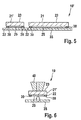
- a substrate assembly 10 is shown, which is released by means of a nozzle 40 from the carrier 35.
- the detachment of the substrate 20 together with the Vorfixierstoff 30 and the bonding material 25 from the carrier 35 can be performed for example in the context of a pick and place process using the nozzle 40.
- FIGS. 7 to 9 show a method for connecting an electronic component 50 to a substrate assembly 10 according to a first embodiment of the invention.
- the substrate assembly 10 is first removed by means of the nozzle 40 from a carrier 35.
- the substrate arrangement 10 is positioned with the aid of the nozzle 40 on the electronic component 50 such that the first side 22 of the substrate 20 is arranged facing the electronic component 50.
- the nozzle 40 acts on the second side 23 of the substrate 20.
- the substrate assembly 10 is placed on the electronic component 50, wherein only the Vorfixierstoff 30 touches the component 50 or only the Vorfixierstoff 30 is connected to the component 50.
- the illustrated component 50 may be, for example, a silicon semiconductor. Between the contacting material 25 and the component 50 is formed a distance, this distance being formed due to the different thicknesses of the prefixing agent and the contacting means.
- nozzle 40 is already removed from the substrate arrangement 10. There is a heat application at a temperature of 100 to 150 ° C. As a result, the prefixing agent 30 is activated so that a prefixing of the substrate assembly 10 to the electronic component 50 takes place.
- the prefixing is preferably an adhesive bond between the substrate 20, in particular the first side 22 of the substrate 20, and the electronic component 50, in particular the side 52 of the electronic component 50 facing the substrate 20, wherein the adhesive bond is produced on the basis of the prefixing means 30 is.
- the pre-drying or the drying step, as this in Fig. 4 is shown is optional. It is possible for the prefixing agent 30 to be applied to the first side 22 of the substrate 20, after which a prefixing of an electronic component 50, 51 to the substrate arrangement 10 takes place immediately thereafter. The formation of a carrier 35 is not necessary in this case. In this case, the prefixing agent 30 is applied to the substrate 20 immediately prior to placement on an electronic component 50, 51 or directly prior to placement on an electronic component 50, 51.
- the actual connection of the substrate assembly 10 takes place with the electronic component 50.
- the bonding can be done by soldering or pressing or sintering.
- the substrate assembly 10 is sintered to the electronic component 50.
- the organic / polymeric components of the prefixing agent 30 volatilize as much as possible. In other words, the prefixing agent 30 is at least partially removed, in particular burned off and / or melted off, during bonding or after bonding.
- residues 31 of the prefixing agent 30 are formed on the first side 52 of the electronic component.
- FIGS. 10 to 12 A method for connecting electronic components 50 and 51 to a substrate arrangement 10 according to a further exemplary embodiment is shown.
- a substrate arrangement 10 comprising two substrate sections 21 and 21 'is equipped with a first electronic component 50 and a second electronic component 51. Both the substrate section 21 and the substrate section 21 'comprise a contacting material 25 and prefixing means 30 formed laterally of the respective contacting material 25.
- Both the first electronic component 50 and the second electronic component 51 are positioned with the aid of nozzles 40 and 40 'to the substrate arrangement 10 such that the first side 22 of the substrate 20 is arranged facing the first electronic component 50 and the second electronic component 51.
- the first electronic component 50 may be a silicon semiconductor.
- the second electronic component 51 has a coating 54 both on the first side 52 and on the second side 53.
- FIG. 11 there is a prefixing of the substrate assembly 10 with the first electronic component 50 and the second electronic component 51 by the on the first side 22 of the substrate 20 partially applied Vorfixierstoff 30.
- Vorfixierstoffs 30 apply in connection with the FIGS. 1 to 9 listed explanations.
- the substrate arrangement 10 is joined together with the first electronic component 50 and the second electronic component 52 exposed to heat, especially at temperatures of 100 to 150 ° C.
- the result is an adhesive bond between the first electronic component 50 and the substrate 20, in particular between the first electronic component 50 and the first side 22 of the substrate 20.
- the substrate assembly 10 is connected to the first electronic component 50 and the second electronic component 51.
- the prefixing agent 30 is at least partially removed, in particular burned off and / or melted off.
- this remaining residue 31 of the prefixing agent 30 is the inorganic fillers of the original prefixing agent 30.
- the electronic component 50 and the second electronic component 51 are in Fig. 12 completely connected to the substrate assembly 10.
- the substrate assembly 10 includes a substrate 20 having a first side 22 and a second side 23. On the first side 22 of the substrate 20 is the remainder 31 of an original prefixing agent 30.
Abstract
Verfahren zum Herstellen einer Substratanordnung (10, 10') zur Verbindung mit einem Elektronikbauteil (50; 51), umfassend die Schritte: - Bereitstellen eines Substrates (20), insbesondere eines DCB-Substrats, eines PCB-Substrats oder eines Leadframes, mit einer ersten Seite (22) und einer zweiten Seite (23), - abschnittsweises Aufbringen eines Vorfixiermittels (30) auf die erste Seite (22) des Substrates (20). Die Erfindung betrifft auch eine entsprechende Substratanordnung (10, 10') sowie ein entsprechendes Verfahren zum Verbinden eines Elektronikbauteils (50, 51) mit der Substratanordnung (10, 10'). Durch die erfindungsgemäßen Maßnahmen wird beim Transport vom Ort des Bestückens der Substratanordnung (10, 10') mit dem Elektronikbauteil (50, 51') zum Ort des Verbindens eine ausreichende Transportfestigkeit erzeugt. Das Vorfixiermittel (30) kann auch alternativ oder zusätzlich auf die erste Seite (52) des Elektronikbauteils (50, 51) abschnittsweise aufgebracht werden. Auf die Substratanordnung (10, 10') und/oder auf das Elektronikbauteil (50, 51) kann vor dem Aufbringen des Vorfixiermittels (30) ein Kontaktierungsmaterial (25) aufgebracht werden. Das Vorfixiermittel (30) kann zumindest abschnittsweise seitlich des Kontaktierungsmaterials (25) aufgebracht werden, derart, dass das Vorfixiermittel (30) dicker als das Kontaktierungsmaterial (25) ist. Nach dem Verbinden kann auf der ersten Seite (22) des Substrates (20) und/oder auf der dem Substrat (20) zugewandten ersten Seite (52) des Elektronikbauteils (50, 51) abschnittsweise ein Rest (31) des Vorfixiermittels (30) ausgebildet sein.Method for producing a substrate arrangement (10, 10 ') for connection to an electronic component (50, 51), comprising the steps: Providing a substrate (20), in particular a DCB substrate, a PCB substrate or a leadframe, with a first side (22) and a second side (23), - Partial application of a Vorfixiermittels (30) on the first side (22) of the substrate (20). The invention also relates to a corresponding substrate arrangement (10, 10 ') and to a corresponding method for connecting an electronic component (50, 51) to the substrate arrangement (10, 10'). By means of the measures according to the invention, a sufficient transporting strength is generated during transport from the place of placement of the substrate arrangement (10, 10 ') with the electronic component (50, 51') to the place of connection. The prefixing means (30) may alternatively or additionally be applied in sections to the first side (52) of the electronic component (50, 51). A contacting material (25) can be applied to the substrate arrangement (10, 10 ') and / or to the electronic component (50, 51) before the application of the prefixing agent (30). The prefixing agent (30) can be applied at least in sections laterally of the contacting material (25) such that the prefixing agent (30) is thicker than the contacting material (25). After joining, a remainder (31) of the prefixing means (30) can be provided in sections on the first side (22) of the substrate (20) and / or on the first side (52) of the electronic component (50, 51) facing the substrate (20). be educated.
Description
Die Erfindung bezieht sich auf ein Verfahren zum Herstellen einer Substratanordnung zur Verbindung mit einem Elektronikbauteil. Des Weiteren betrifft die Erfindung eine Substratanordnung zur Verbindung mit einem Elektronikbauteil. Außerdem betrifft die Erfindung ein Verfahren zum Verbinden eines Elektronikbauteils mit einer Substratanordnung. Des Weiteren betrifft die Erfindung ein Verfahren zum Verbinden eines Elektronikbauteils mit einem Substrat. Ferner betrifft die Erfindung ein Elektronikbauteil, das mit einer Substratanordnung verbunden ist.The invention relates to a method for producing a substrate arrangement for connection to an electronic component. Furthermore, the invention relates to a substrate arrangement for connection to an electronic component. Moreover, the invention relates to a method for connecting an electronic component to a substrate arrangement. Furthermore, the invention relates to a method for connecting an electronic component to a substrate. Furthermore, the invention relates to an electronic component which is connected to a substrate arrangement.
In der Leistungselektronik ist es bekannt, Substrate oder Bauteile mit getrockneter Sinterpaste bereitzustellen, die beispielsweise von einem Kunden nur noch appliziert werden müssen. Innerhalb des Fertigungsprozesses können Bauteile, insbesondere Elektronikbauteile, die an ein Substrat mit vorgetrockneter Sinterpaste angeheftet sind, beim Transport vom Ort des Bestückens zum Ort des Sinterns verrutschen.In power electronics, it is known to provide substrates or components with dried sintering paste, which only have to be applied by a customer, for example. Within the manufacturing process, components, in particular electronic components, which are attached to a substrate with pre-dried sintering paste can slip during transport from the place of placement to the place of sintering.
Diesbezüglich ist es bekannt, dass die Bauteile, insbesondere Elektronikbauteile, auf die getrocknete Sinterpaste bei gleichzeitiger Wärmebeaufschlagung aufgesetzt werden. Es hat sich herausgestellt, dass ein derartiges warmes Bestücken bei einer Vielzahl von Elektronikbauteilen nur eine unzureichende Transportfestigkeit hervorruft, da die Adhäsion aufgrund gebogener Bauteile und/oder verschmutzter Oberflächen und/oder ungünstiger Oberflächen nicht ausreicht, um einen sicheren Transport vom Ort des Bestückens zum Ort des Sinterns zu ermöglichen. Daher ist es bekannt, die bestückten, aber noch nicht verlöteten bzw. versinterten Elektronikbauteile durch Masken oder Formen zu fixieren oder durch Federn aufwendig zu klemmen.In this regard, it is known that the components, in particular electronic components, are placed on the dried sintered paste with simultaneous heat application. It has been found that such a warm placement in a variety of electronic components only insufficient transport resistance causes because the adhesion due to curved components and / or dirty surfaces and / or unfavorable surfaces not sufficient to allow safe transport from the place of placement to the place of sintering. Therefore, it is known to fix the assembled, but not yet soldered or sintered electronic components by masks or shapes or to clamp consuming by springs.
Ausgehend von diesem Stand der Technik ist es die Aufgabe der vorliegenden Erfindung ein Verfahren zum Herstellen einer Substratanordnung zur Verbindung mit einem Elektronikbauteil anzugeben, sodass beim Transport vom Ort des Bestückens zum Ort des Sinterns der Elektronikbauteile eine ausreichende Transportfestigkeit erzeugt wird.Based on this prior art, it is the object of the present invention to provide a method for producing a substrate arrangement for connection to an electronic component, so that a sufficient transport strength is generated during transport from the place of placement to the location of the sintering of the electronic components.
Des Weiteren ist es Aufgabe der vorliegenden Erfindung eine Substratanordnung zur Verbindung mit einem Elektronikbauteil anzugeben, wobei die Substratanordnung derart ausgebildet ist, dass ein bestücktes, aber noch nicht verlötetes bzw. versintertes Bauteil auf der Substratanordnung eine ausreichende Transportfestigkeit aufweist.Furthermore, it is an object of the present invention to specify a substrate arrangement for connection to an electronic component, wherein the substrate arrangement is designed such that a populated, but not yet soldered or sintered component on the substrate arrangement has sufficient transport strength.
Des Weiteren ist es eine Aufgabe der vorliegenden Erfindung ein Verfahren zum Verbinden eines Elektronikbauteils mit einer Substratanordnung anzugeben. Ferner ist es Aufgabe der Erfindung, ein Elektronikbauteil das mit einer Substratanordnung verbunden ist, anzugeben.Furthermore, it is an object of the present invention to provide a method for connecting an electronic component to a substrate arrangement. It is a further object of the invention to specify an electronic component which is connected to a substrate arrangement.
Erfindungsgemäß wird diese Aufgabe mit Blick auf das Verfahren zum Herstellen einer Substratanordnung zur Verbindung mit einem Elektronikbauteil durch den Gegenstand des Anspruchs 1, mit Blick auf die Substratanordnung durch den Gegenstand des Anspruchs 7, mit Blick auf das Verfahren zum Verbinden eines Elektronikbauteils mit einer Substratanordnung durch den Gegenstand des Anspruchs 12, mit Blick auf das Verfahren zum Verbinden eines Elektronikbauteils mit einem Substrat durch den Gegenstand des Anspruchs 16 und mit Blick auf das Elektronikbauteil durch den Gegenstand des Anspruchs 19 gelöst.According to the invention, this object is achieved with regard to the method for producing a substrate arrangement for connection to an electronic component by the subject of claim 1, with a view to the substrate arrangement by the subject of claim 7, with regard to the method for connecting an electronic component with a substrate arrangement the subject-matter of claim 12, with regard to the method for connecting an electronic component to a substrate by the subject-matter of claim 16 and with regard to the electronic component by the subject-matter of claim 19.
Die Erfindung beruht auf dem Gedanken, ein Verfahren zum Herstellen einer Substratanordnung zur Verbindung mit einem Elektronikbauteil anzugeben, das folgende Schritte umfasst:
- Bereitstellen eines Substrates, insbesondere eines DCB-Substrats oder eines PCB-Substrats oder eines Leadframes, mit einer ersten Seite und einer zweiten Seite,
- abschnittsweises Aufbringen eines Vorfixiermittels auf die erste Seite des Substrates.
- Providing a substrate, in particular a DCB substrate or a PCB substrate or a leadframe, with a first side and a second side,
- section-wise application of a prefixing agent to the first side of the substrate.
Die mit Hilfe des erfindungsgemäßen Verfahrens hergestellte Substratanordnung dient zur nachfolgenden Verbindung mit einem Elektronikbauteil.The substrate arrangement produced with the aid of the method according to the invention serves for the subsequent connection to an electronic component.
In einer bevorzugten Ausführungsform des erfindungsgemäßen Verfahrens wird auf die erste Seite des Substrates, insbesondere vor dem Aufbringen des Vorfixiermittels, abschnittsweise ein Kontaktierungsmaterial aufgebracht. Das Kontaktierungsmaterial bedeckt die erste Seite des Substrates nicht vollständig. Sowohl das Vorfixiermittel als auch das Kontaktierungsmaterial sind auf der ersten Seite des Substrates aufgebracht.In a preferred embodiment of the method according to the invention, a contacting material is applied in sections to the first side of the substrate, in particular before the application of the prefixing agent. The bonding material does not completely cover the first side of the substrate. Both the prefixing agent and the contacting material are applied on the first side of the substrate.
Das Kontaktierungsmaterial, das eine Sinterpaste, insbesondere eine silberhaltige Sinterpaste, oder ein Lot oder ein Leitkleber oder eine Klebefolie ist, dient zum tatsächlichen Verbinden des Substrates mit dem Elektronikbauteil. Das Vorfixiermittel dient lediglich zur Vorfixierung bzw. zu einem vorübergehenden Anheften des Substrates an dem Elektronikbauteil oder des Elektronikbauteils an dem Substrat. Aufgrund des Vorfixierens bzw. Anheftens wird eine ausreichende Transportfähigkeit des Bauteils vom Ort des Bestückens zum Ort des Sinterns hervorgerufen. Das Vorfixiermittel ist ein temporäres Fixiermittel. Mit anderen Worten ist das Vorfixiermittel ein Fixiermittel, das eine vorübergehende Fixierung einer Substratanordnung bzw. eines Substrates mit einem Elektronikbauteil ermöglicht.The contacting material, which is a sintering paste, in particular a silver-containing sintering paste, or a solder or a conductive adhesive or an adhesive film, serves for the actual bonding of the substrate to the electronic component. The prefixing agent serves only for prefixing or for temporarily adhering the substrate to the electronic component or the electronic component to the substrate. Due to the Vorfixierens or attachment sufficient transportability of the component from the place of placement is caused to the place of sintering. The prefixing agent is a temporary fixing agent. In other words, the prefixing agent is a fixing agent, which allows a temporary fixation of a substrate arrangement or a substrate with an electronic component.
Bei dem Vorfixiermittel kann es sich um ein Lot und/oder um ein Klebemittel handeln. Insbesondere ist das Vorfixiermittel ein Klebemittel, das 20 bis 45 Gew.-% thermoplastisches Polymer und 40 bis 70 Gew.-% organisches Lösemittel und 10 bis 25 Gew.-% anorganische Füllstoffpartikel und 0 bis 0,5 Gew.-% weitere Additive aufweist.The prefixing agent may be a solder and / or an adhesive. In particular, the prefixing agent is an adhesive comprising 20 to 45% by weight of thermoplastic polymer and 40 to 70% by weight of organic solvent and 10 to 25% by weight of inorganic filler particles and 0 to 0.5% by weight of other additives ,
Das thermoplastische Polymer des Vorfixiermittels weist beispielsweise eine Glasübergangstemperatur von 60 bis 120 °C auf. Die Bestimmung der Glasübergangstemperatur wird mittels DDK, nämlich mittels dynamischer Differenzkalorimetrie, bzw. mittels DSC, nämlich differential scanning calorimetry, bei einer Aufheizrate von 10 K/Minute durchgeführt.
Bei dem thermoplastischen Polymer kann es sich insbesondere um (Meth)acrylcopolymere handeln. Der Molmassenbereich der thermoplastischen (Meth)acrylcopolymere kann 35.000 bis 70.000 g/mol betragen (Mw= 35.000 bis 70.000 g/mol). Der Molmassenbereich ist mittels Gelpermeationschromatographie (GPC) zu bestimmen. Für die Gelpermeationschromatographie gilt: Polystyrolgel als stationäre Phase, Tetrahydrofuran als mobile Phase, Polystyrolstandards.The thermoplastic polymer of the prefixing agent has, for example, a glass transition temperature of 60 to 120 ° C. The determination of Glass transition temperature is carried out by means of DDK, namely by means of differential scanning calorimetry, or by means of DSC, namely differential scanning calorimetry, at a heating rate of 10 K / minute.
The thermoplastic polymer may in particular be (meth) acrylic copolymers. The molecular weight range of the thermoplastic (meth) acrylic copolymers may be 35,000 to 70,000 g / mol (Mw = 35,000 to 70,000 g / mol). The molecular weight range can be determined by gel permeation chromatography (GPC). For gel permeation chromatography, the following applies: polystyrene gel as the stationary phase, tetrahydrofuran as the mobile phase, polystyrene standards.
Die 40 bis 70 Gew.-% organische Lösemittel weisen 30 bis 100 Gew.-% Terpineole auf.The 40 to 70 wt .-% of organic solvents have 30 to 100 wt .-% terpineols.
Die 10 bis 25 Gew.-% anorganische Füllstoffpartikel weisen eine Teilchengröße (d50) von 5 bis 20 µm, bevorzugt von 5 bis 10 µm, auf. Bei diesen anorganischen Füllstoffpartikel kann es sich beispielsweise um Aluminiumoxid und/oder Siliziumdioxid handeln. Die Bestimmung der Teilchengröße (d50) erfolgt vorzugsweise mittels eines Laserbeugungsverfahrens.The 10 to 25 wt .-% inorganic filler particles have a particle size (d50) of 5 to 20 .mu.m, preferably from 5 to 10 .mu.m. These inorganic filler particles may be, for example, aluminum oxide and / or silicon dioxide. The determination of the particle size (d50) is preferably carried out by means of a laser diffraction method.
Bei den 0 bis 0,5 Gew.-% weitere Additive kann es sich beispielsweise um Benetzungsmittel handeln.The 0 to 0.5 wt .-% further additives may be, for example, wetting agent.
Mit Hilfe eines Klebemittels, insbesondere mit Hilfe eines Klebemittels mit angegebener Zusammensetzung bzw. mit angegebener Formulierung, können gleichmäßige Vorfixiermittelpunkte, insbesondere Klebepunkte, mit kalkulierbarer Endhöhe erzeugt werden.By means of an adhesive, in particular with the aid of an adhesive having the specified composition or formulation, it is possible to produce uniform prefixing centers, in particular adhesive dots, with a calculable final height.
Das Vorfixiermittel kann durch Dispensen oder Dippen oder Jetten auf die erste Seite des Substrates aufgebracht werden. Insbesondere wird das Vorfixiermittel in Form von halbkugelförmigen Klebepunkten bzw. halbkugelförmigen Punkten aufgebracht.The prefixing agent can be applied to the first side of the substrate by dispensing or dipping or jetting. In particular, the prefixing agent is applied in the form of hemispherical adhesive dots or hemispherical dots.
Das Kontaktierungsmaterial kann eine Sinterpaste, insbesondere eine silberhaltige Sinterpaste, oder ein Lot oder ein Leitkleber oder eine Klebefolie sein.The contacting material may be a sintering paste, in particular a silver-containing sintering paste, or a solder or a conductive adhesive or an adhesive film.
Das auf das Substrat aufgebrachte Vorfixiermittel, insbesondere das auf das Substrat aufgebrachte Vorfixiermittel und das auf das Substrat aufgebrachte Kontaktierungsmaterial, kann getrocknet werden bzw. können getrocknet werden. Mit anderen Worten wird das Substrat mit dem aufgebrachten Vorfixiermittel und/oder dem aufgebrachten Kontaktierungsmaterial einem Trocknungsprozess ausgesetzt. Das Trocknen kann bei 100 bis 150 °C Objekttemperatur für 2 bis 30 Minuten durchgeführt werden.The prefixing agent applied to the substrate, in particular the prefixing agent applied to the substrate and the contacting material applied to the substrate, can be dried or can be dried. In other words, the substrate with the applied prefixing agent and / or the applied contacting material is subjected to a drying process. The drying can be carried out at 100 to 150 ° C object temperature for 2 to 30 minutes.
Sofern ein Trocknen bzw. Vortrocknen durchgeführt wird, wird die Dicke des aufgebrachten Vorfixiermittels nach dem Trocknen bzw. Vortrocknen bzw. aufgrund des Trocknens bzw. Vortrocknens reduziert.If drying or predrying is carried out, the thickness of the applied prefixing agent is reduced after drying or predrying or drying.
In einer weiteren Ausführungsform der Erfindung kann das Substrat mit aufgebrachtem Vorfixiermittel, insbesondere mit aufgebrachten Vorfixiermittel und aufgebrachtem Kontaktierungsmaterial, auf einem Träger derart positioniert werden, dass die erste Seite des Substrates dem Träger zugewandt angeordnet ist, wobei das Vorfixiermittel und/oder das Kontaktierungsmaterial mit dem Träger zumindest haftverbunden wird bzw. werden. Das Substrat kann folglich auf einem Träger aufgebracht werden, sodass die Substratanordnung, die ein Substrat, ein Vorfixiermittel, optional ein Kontaktierungsmaterial und optional einen Träger umfasst, zu einer weiteren Produktionsstätte bzw. zu einer weiteren Verarbeitungsvorrichtung transportiert werden kann. Es ist möglich, dass lediglich das Vorfixiermittel mit dem Träger haftverbunden ist. Zwischen dem Träger und einem optional vorhandenen Kontaktierungsmaterial kann beispielsweise ein geringer Abstand bestehen.In a further embodiment of the invention, the substrate with the prefixing agent applied, in particular with applied prefixing agent and applied contacting material, can be positioned on a carrier such that the first side of the substrate faces the carrier, wherein the prefixing agent and / or the contacting material with the Carrier is at least adherent or will be. The substrate can consequently be applied to a carrier so that the substrate arrangement, which comprises a substrate, a prefixing agent, optionally a contacting material and optionally a carrier, can be transported to a further production facility or to a further processing apparatus. It is possible that only the prefixing agent is adhesively bonded to the carrier. For example, there may be a small distance between the carrier and an optional contacting material.
Das Vorfixiermittel ist zumindest abschnittsweise seitlich des Kontaktierungsmaterials auf die erste Seite des Substrates aufgebracht. Das Vorfixiermittel kann seitlich des Kontaktierungsmaterials mittels Dispensen, Dippen oder Jetten aufgebracht werden. Beispielsweise kann das Vorfixiermittel als mindestens ein Klebepunkt seitlich des Kontaktierungsmaterials aufgebracht werden. Des Weiteren ist es denkbar, dass das Vorfixiermittel balkenförmig seitlich des Kontaktierungsmaterials auf die erste Seite des Substrates aufgebracht wird. Ebenso ist es möglich, dass das Kontaktierungsmaterial vollseitenumfänglich von einem Vorfixiermittel umgeben ist.The prefixing agent is applied at least in sections laterally of the contacting material on the first side of the substrate. The prefixing agent can be applied to the side of the contacting material by means of dispensing, dipping or jetting. By way of example, the prefixing agent can be applied as at least one adhesive point to the side of the contacting material. Furthermore, it is conceivable that the prefixing agent is applied in the form of a beam to the side of the contacting material on the first side of the substrate. It is likewise possible for the contacting material to be surrounded by a prefixing agent on the full side.
Das Vorfixiermittel kann derart auf die erste Seite des Substrates aufgebracht werden, dass das Vorfixiermittel dicker als das Kontaktierungsmaterial ist. Mit anderen Worten steht das Vorfixiermittel in vertikaler Richtung über das Kontaktierungsmaterial über. Das Vorfixiermittel weist eine größere Materialdicke als das Kontaktierungsmaterial auf. Das Vorfixiermittel ist vor einem optionalen Trocknen bzw. Vortrocknen dicker als nach dem Trocknen bzw. Vortrocknen.The prefixing agent may be applied to the first side of the substrate such that the prefixing agent is thicker than the contacting material. In other words, the prefixing agent projects over the contacting material in the vertical direction. The prefixing agent has a greater material thickness than the contacting material. The prefixer is thicker before optional drying or pre-drying than after drying or predrying.
Die Erfindung beruht des Weiteren auf dem Gedanken, eine Substratanordnung zur Verbindung mit einem Elektronikbauteil anzugeben, wobei die Substratanordnung vorzugsweise mit einem vorerwähnten erfindungsgemäßen Verfahren hergestellt ist. Die erfindungsgemäße Substratanordnung umfasst ein Substrat mit einer ersten Seite und einer zweiten Seite, wobei auf der ersten Seite des Substrats abschnittsweise ein Vorfixiermittel aufgebracht ist.The invention is further based on the idea of specifying a substrate arrangement for connection to an electronic component, wherein the substrate arrangement is preferably produced by a method according to the invention mentioned above. The substrate arrangement according to the invention comprises a substrate having a first side and a second side, wherein a prefixing agent is applied in sections on the first side of the substrate.
Bei dem Substrat kann es sich um ein DCB-Substrat oder PCB-Substrat oder einen Leadframe handeln. Mit anderen Worten kann das Substrat ein DCB-Substrat oder ein PCB-Substrat oder ein Leadframe sein.The substrate may be a DCB substrate or PCB substrate or a leadframe. In other words, the substrate may be a DCB substrate or a PCB substrate or a leadframe.
Das Vorfixiermittel kann ein Lot und/oder ein Klebemittel sein. Insbesondere handelt es sich bei dem Vorfixiermittel um ein Klebemittel, das 20 bis 45 Gew.-% thermoplastisches Polymer und 40 bis 70 Gew.-% organisches Lösemittel und 10 bis 25 Gew.-% anorganische Füllstoffpartikel und 0 bis 0,5 Gew.-% weitere Additive aufweist. Bezüglich des Klebemittels und der Zusammensetzung sowie hinsichtlich der Verfahren zur Bestimmung einzelner Parameter des Klebemittels wird auf die bereits angeführten Erläuterungen im Zusammenhang mit dem vorerwähnten Verfahren verwiesen. Diese Erläuterungen gelten auch für die Substratanordnung.The prefixing agent may be a solder and / or an adhesive. In particular, the prefixing agent is an adhesive comprising 20 to 45% by weight of thermoplastic polymer and 40 to 70% by weight of organic solvent and 10 to 25% by weight of inorganic filler particles and 0 to 0.5% by weight. % has further additives. With regard to the adhesive and the composition and with regard to the methods for determining individual parameters of the adhesive, reference is made to the explanations already given in connection with the aforementioned method. These explanations also apply to the substrate arrangement.
Auf der ersten Seite des Substrates ist vorzugsweise außerdem abschnittsweise ein Kontaktierungsmaterial aufgebracht. Auf der ersten Seite des Substrates kann somit sowohl ein Vorfixiermittel als auch ein Kontaktierungsmaterial aufgebracht sein. Das Vorfixiermittel dient in einem Verfahren zum Aufbringen eines Elektronikbauteils zu einer Vorfixierung des Elektronikbauteils auf der Substratanordnung. Das Kontaktierungsmaterial dient hingegen zur tatsächlichen Fixierung bzw. zum tatsächlichen und dauerhaften Verbinden der Substratanordnung mit dem Elektronikbauteil.On the first side of the substrate, a contacting material is preferably also applied in sections. Thus, both a prefixing agent and a contacting material can be applied to the first side of the substrate. The prefixing agent is used in a method for applying an electronic component to a prefixing of the electronic component on the substrate assembly. The contacting material, however, serves for the actual fixation or for the actual and permanent connection of the substrate arrangement to the electronic component.
Das Kontaktierungsmaterial kann eine Sinterpaste, insbesondere eine silberhaltige Sinterpaste, oder ein Lot oder ein Leitkleber oder eine Klebefolie sein.The contacting material may be a sintering paste, in particular a silver-containing sintering paste, or a solder or a conductive adhesive or an adhesive film.
Das Vorfixiermittel ist zumindest abschnittsweise seitlich des Kontaktierungsmaterials auf der ersten Seite des Substrates aufgebracht. Das Vorfixiermittel kann tropfenförmig, halbkugelförmig oder balkenförmig seitlich des Kontaktierungsmaterials ausgebildet sein. In einer Ausführungsform der Erfindung ist es möglich, dass das Kontaktierungsmaterial voll seitenumfänglich von dem Vorfixiermittel umrandet bzw. umgeben ist.The prefixing agent is applied at least in sections laterally of the contacting material on the first side of the substrate. The prefixing agent may be formed drop-shaped, hemispherical or bar-shaped laterally of the contacting material. In one embodiment of the invention, it is possible for the contacting material to be surrounded or surrounded by the prefixing means to the full extent of the side.
Das Vorfixiermittel ist vorzugsweise dicker als das Kontaktierungsmaterial ausgebildet. Mit anderen Worten steht das Vorfixiermittel in vertikaler Richtung über das Kontaktierungsmaterial hinaus.The prefixing agent is preferably formed thicker than the contacting material. In other words, the prefixing agent protrudes vertically beyond the bonding material.
In einer weiteren Ausführungsform weist die Substratanordnung einen Träger auf, der mit dem Vorfixiermittel und/oder mit dem Kontaktierungsmaterial zumindest haftverbunden ist. Das Substrat ist in Relation zu dem Träger derart angeordnet, dass die erste Seite des Substrates dem Träger zugewandt angeordnet ist. Der Träger dient dazu, dass die Substratanordnung von einer ersten Produktionsstätte zu einer weiteren Produktionsstätte bzw. von einer ersten Fertigungsvorrichtung zu einer weiteren Fertigungsvorrichtung transportiert werden kann. Bei dem Träger kann es sich beispielsweise um eine Trägerfolie mit geringer Adhäsionskraft handeln.In a further embodiment, the substrate arrangement has a carrier which is at least adhesively bonded to the prefixing agent and / or to the contacting material. The substrate is arranged in relation to the carrier such that the first side of the substrate is disposed facing the carrier. The carrier serves to transport the substrate arrangement from a first production site to a further production site or from a first production device to a further production device. The carrier may be, for example, a carrier film with a low adhesive force.
Die Erfindung beruht des Weiteren auf dem Gedanken, ein Verfahren zum Verbinden eines Elektronikbauteils mit einer Substratanordnung anzugeben. Bei der Substratanordnung kann es sich insbesondere um eine erfindungsgemäße Substratanordnung und/oder um eine Substratanordnung, die mit Hilfe des beschriebenen erfindungsgemäßen Verfahrens hergestellt wurde, handeln. Das erfindungsgemäße Verfahren zum Verbinden eines Elektronikbauteils mit einer Substratanordnung umfasst die Schritte:
- Positionieren der Substratanordnung und des Elektronikbauteil zueinander derart, dass eine/die erste Seite des Substrates dem Elektronikbauteil zugewandt angeordnet ist,
- Vorfixieren der Substratanordnung auf dem Elektronikbauteil durch ein/das auf der ersten Seite des Substrates abschnittsweise aufgebrachte(s) Vorfixiermittel,
- Verbinden der Substratanordnung mit dem Elektronikbauteil.
- Positioning the substrate arrangement and the electronic component relative to one another in such a way that one / the first side of the substrate is arranged facing the electronic component,
- Prefixing the substrate assembly on the electronic component by / on the first side of the substrate partially applied (s) prefixing,
- Connecting the substrate assembly to the electronic component.
Das Positionieren der Substratanordnung und des Elektronikbauteils zueinander derart, dass eine/die erste Seite des Substrates dem Elektronikbauteil zugewandt angeordnet ist, kann zum einen derart ausgeführt werden, dass die Substratanordnung auf das Elektronikbauteil aufgesetzt wird. In einer weiteren Ausführungsform ist es denkbar, dass das Elektronikbauteil auf der Substratanordnung aufgebracht wird.The positioning of the substrate arrangement and of the electronic component relative to one another in such a way that one / the first side of the substrate is arranged facing the electronic component can on the one hand be carried out such that the substrate arrangement is placed on the electronic component. In a further embodiment, it is conceivable that the electronic component is applied to the substrate arrangement.
Nach dem Positionieren der Substratanordnung und dem Elektronikbauteil zueinander wird ein Vorfixieren der Substratanordnung mit dem Elektronikbauteil vorgenommen. Dieses Vorfixieren wird mit Hilfe des auf der ersten Seite des Substrates abschnittsweise aufgebrachten Vorfixiermittels durchgeführt. Hierzu erfolgt vorzugsweise eine Wärmebeaufschlagung. Vorzugsweise wird eine Temperatur von 100 bis 150 °C aufgebracht, sodass das Vorfixiermittel über die aufgebrachte Wärme aktiviert wird und somit die Substratanordnung mit dem Elektronikbauteil vorfixiert werden kann. Aufgrund des Vorfixierens kann eine derartige Transportfestigkeit hinsichtlich des mit der Substratanordnung vorfixiert verbundenen Elektronikbauteils erzielt werden, dass das Elektronikbauteil nicht mehr aufgrund des Vorschubs eines Transportbandes losgeschüttelt werden kann. Vielmehr bleibt das Elektronikbauteil in der vorfixierten Lage.After the positioning of the substrate arrangement and the electronic component relative to one another, the substrate arrangement is prefixed to the electronic component. This prefixing is carried out with the aid of the prefixing agent applied in sections on the first side of the substrate. For this purpose, preferably a heat application. Preferably, a temperature of 100 to 150 ° C is applied, so that the prefixing agent is activated by the applied heat and thus the substrate assembly can be prefixed with the electronic component. Due to the prefixing, such transportability can be achieved with respect to the electronic component prefixed to the substrate arrangement such that the electronic component can no longer be shaken loose due to the advance of a conveyor belt. Rather, the electronic component remains in the prefixed position.
Bei dem Elektronikbauteil kann es sich um einen Halbleiter oder ein DCB-Substrat oder ein PCB-Substrat handeln. Mit anderen Worten kann das Elektronikbauteil ein Halbleiter oder ein DCB-Substrat oder ein PCB-Substrat sein.The electronic component may be a semiconductor or a DCB substrate or a PCB substrate. In other words, the electronic component may be a semiconductor or a DCB substrate or a PCB substrate.
Zeitlich nach dem Vorfixieren erfolgt das Verbinden der Substratanordnung mit dem Elektronikbauteil. Das Verbinden der Substratanordnung mit dem Elektronikbauteil kann beispielsweise mittels Versintern oder Verpressen oder Verlöten erfolgen. Vorzugsweise wird die Substratanordnung mit dem Elektronikbauteil versintert. Hierzu weist die Substratanordnung ein Kontaktierungsmaterial, insbesondere eine Sinterpaste, auf.After the prefixing, the bonding of the substrate arrangement to the electronic component takes place. The bonding of the substrate arrangement to the electronic component can be effected, for example, by sintering or pressing or soldering. Preferably, the substrate assembly is sintered with the electronic component. For this purpose, the substrate arrangement has a contacting material, in particular a sintering paste.
Bezüglich des Vorfixiermittels im Zusammenhang mit dem erfindungsgemäßen Verfahren zum Verbinden eines Elektronikbauteils mit einer Substratanordnung wird auf die bereits aufgeführten Erläuterungen hinsichtlich des Vorfixiermittels verwiesen. Auch hinsichtlich der Anordnung des Vorfixiermittels und des Kontaktierungsmaterials zueinander wird auf die bereits aufgeführten Erläuterungen verwiesen.With regard to the prefixing agent in connection with the method according to the invention for connecting an electronic component to a substrate arrangement, reference is made to the explanations already given regarding the prefixing agent. Also with regard to the arrangement of the prefixing agent and the contacting material to each other, reference is made to the explanations already given.
Vorzugsweise wird die mit dem Elektronikbauteil fixierte Substratanordnung zum Verbinden der Substratanordnung mit dem Elektronikbauteil in einen Prozessofen transportiert. Bei dem Prozessofen kann es sich beispielsweise um einen Drucksinterofen oder einen Reflowofen oder einen Laminierofen handeln. Während des Sinterns oder während des Drucksinterns verflüchtigen sich die organischen und/oder polymeren Bestandteile des Vorfixiermittels weitestgehend. Die organischen und/oder polymeren Bestandteile des Vorfixiermittels werden verdampft und/oder thermisch zersetzt. Während des Verbindens der Substratanordnung mit dem Elektronikbauteil wird die Verbindung des Vorfixiermittels zum Elektronikbauteil entfernt, insbesondere abgebrannt und/oder abgeschmolzen.Preferably, the substrate assembly fixed to the electronic component is transported to connect the substrate assembly to the electronic component in a process furnace. The process furnace can be, for example, a pressure sintering furnace or a reflow oven or a laminating oven. During sintering or during pressure sintering, the organic and / or polymeric constituents of the prefixing agent volatilize as much as possible. The organic and / or polymeric constituents of the prefixing agent are vaporized and / or thermally decomposed. During the bonding of the substrate arrangement to the electronic component, the connection of the prefixing agent to the electronic component is removed, in particular burned off and / or melted off.
Nach dem Verbinden der Substratanordnung mit dem Elektronikbauteil, insbesondere nach dem Versintern oder Drucksintern und/oder Verlöten und/oder Verspressen, sind auf der ersten Seite der Substratanordnung größtenteils oder ausschließlich die anorganischen Füllstoffe des Vorfixiermittels vorhanden. Es verbleiben somit größtenteils oder ausschließlich die anorganischen Füllstoffe des Vorfixiermittels. Bei dem beschriebenen Vorfixiermittel handelt es sich mit anderen Worten um ein temporäres Fixierungsmittel, das nach dem tatsächlichen Verbinden bzw. tatsächlich dauerhaften Verbinden der Substratanordnung mit dem Elektronikbauteil größtenteils oder vollständig entfernt ist.After connecting the substrate assembly to the electronic component, in particular after sintering or pressure sintering and / or soldering and / or pressing, the inorganic filler of the prefixing agent is present on the first side of the substrate arrangement largely or exclusively. Thus, mostly or exclusively, the inorganic fillers of the prefixing agent remain. In other words, the described prefixing agent is a temporary fixing agent which is largely or completely removed after the actual bonding or actually permanent bonding of the substrate assembly to the electronic component.
Bei der Zusammensetzung des Vorfixiermittels wird vorzugsweise 20 bis 45 Gew.-% thermoplastisches Polymer mit einer derartigen Glasübergangstemperatur gewählt, sodass die Glasübergangstemperatur geringer ist als die Temperatur, die während des Vorfixierens auf die Substratanordnung wirkt, insbesondere geringer ist als die Wärmebeaufschlagung bei Temperaturen von 100 bis 150 °C.In the composition of the prefixing agent, preferably, 20 to 45% by weight of thermoplastic polymer having such a glass transition temperature is selected so that the glass transition temperature is lower than the temperature acting on the substrate assembly during pre-fixing, in particular less than heat application at temperatures of 100 up to 150 ° C.
Ein weiterer Aspekt der Erfindung beruht auf einem Verfahren zum Verbinden eines Elektronikbauteils mit einem Substrat, insbesondere mit einem DCB-Substrat oder einem PCB-Substrat oder einem Leadframe, wobei das Substrat eine erste Seite und eine zweite Seite aufweist und das Verfahren folgende Schritte umfasst:
- Bereitstellen eines Elektronikbauteils mit einer ersten Seite und einer zweiten Seite,
- abschnittsweises Aufbringen eines Vorfixiermittels auf die erste Seite des Elektronikbauteils und/oder auf die erste Seite des Substrats.
- Providing an electronic component having a first side and a second side,
- partially applying a prefixing agent to the first side of the electronic component and / or to the first side of the substrate.
Es ist möglich, dass auf die erste Seite des Substrates und/oder auf die erste Seite des Elektronikbauteils, insbesondere vor dem Aufbringen des Vorfixiermittels, abschnittsweise ein Kontaktierungsmaterial aufgebracht wird. Das Kontaktierungsmaterial bedeckt die erste Seite des Substrates und/oder die erste Seite des Elektronikbauteils nicht vollständig. Sowohl das Vorfixiermittel als auch das Kontaktierungsmaterial können auf der ersten Seite des Kontaktierungsmaterials aufgebracht sein.It is possible for a contacting material to be applied in sections to the first side of the substrate and / or to the first side of the electronic component, in particular prior to the application of the prefixing agent. The bonding material does not completely cover the first side of the substrate and / or the first side of the electronic component. Both the prefixing agent and the contacting material may be applied to the first side of the contacting material.
Das Kontaktierungsmaterial, das eine Sinterpaste, insbesondere eine silberhaltige Sinterpaste, oder ein Lot oder ein Leitkleber oder eine Klebefolie ist, dient zum tatsächlichen Verbinden des Substrates mit dem Elektronikbauteil. Das Vorfixiermittel dient lediglich zur Vorfixierung bzw. zu einem vorübergehenden Anheften des Substrates an dem Elektronikbauteil oder des Elektronikbauteils an dem Substrat. Aufgrund des Vorfixierens bzw. Anheftens wird eine ausreichende Transportfähigkeit des Bauteils vom Ort des Bestückens zum Ort des Sinterns hervorgerufen. Das Vorfixiermittel ist ein temporäres Fixiermittel. Mit anderen Worten ist das Vorfixiermittel ein Fixiermittel, das eine vorübergehende Fixierung eines Substrates mit einem Elektronikbauteil ermöglicht.The contacting material, which is a sintering paste, in particular a silver-containing sintering paste, or a solder or a conductive adhesive or an adhesive film, serves for the actual bonding of the substrate to the electronic component. The prefixing agent serves only for prefixing or for temporarily adhering the substrate to the electronic component or the electronic component to the substrate. Due to the Vorfixierens or attachment sufficient transportability of the component from the place of placement is caused to the place of sintering. The prefixing agent is a temporary fixing agent. In other words, the prefixing agent is a fixing agent that allows temporary fixing of a substrate with an electronic component.
Bei dem Vorfixiermittel kann es sich um ein Lot und/oder um ein Klebemittel handeln. Insbesondere ist das Vorfixiermittel ein Klebemittel, das 20 bis 45 Gew.-% thermoplastisches Polymer und 40 bis 70 Gew.-% organisches Lösemittel und 10 bis 25 Gew.-% anorganische Füllstoffpartikel und 0 bis 0,5 Gew.-% weitere Additive aufweist.The prefixing agent may be a solder and / or an adhesive. In particular, the prefixing agent is an adhesive comprising 20 to 45% by weight of thermoplastic polymer and 40 to 70% by weight of organic solvent and 10 to 25% by weight of inorganic filler particles and 0 to 0.5% by weight of other additives ,
Das thermoplastische Polymer des Vorfixiermittels weist beispielsweise eine Glasübergangstemperatur von 60 bis 120 °C auf. Die Bestimmung der Glasübergangstemperatur wird mittels DDK, nämlich mittels dynamischer Differenzkalorimetrie, bzw. mittels DSC, nämlich differential scanning calorimetry, bei einer Aufheizrate von 10 K/Minute durchgeführt.
Bei dem thermoplastischen Polymer kann es sich insbesondere um (Meth)acrylcopolymere handeln. Der Molmassenbereich der thermoplastischen (Meth)acrylcopolymere kann 35.000 bis 70.000 g/mol betragen (Mw= 35.000 bis 70.000 g/mol). Der Molmassenbereich ist mittels Gelpermeationschromatographie (GPC) zu bestimmen. Für die Gelpermeationschromatographie gilt: Polystyrolgel als stationäre Phase, Tetrahydrofuran als mobile Phase, Polystyrolstandards.The thermoplastic polymer of the prefixing agent has, for example, a glass transition temperature of 60 to 120 ° C. The determination of the glass transition temperature is carried out by means of DDK, namely by means of differential scanning calorimetry, or by means of DSC, namely differential scanning calorimetry, at a heating rate of 10 K / minute.
The thermoplastic polymer may in particular be (meth) acrylic copolymers. The molecular weight range of the thermoplastic (meth) acrylic copolymers may be 35,000 to 70,000 g / mol (Mw = 35,000 to 70,000 g / mol). The molecular weight range can be determined by gel permeation chromatography (GPC). For gel permeation chromatography, the following applies: polystyrene gel as the stationary phase, tetrahydrofuran as the mobile phase, polystyrene standards.
Die 40 bis 70 Gew.-% organische Lösemittel weisen 30 bis 100 Gew.-% Terpineole auf.The 40 to 70 wt .-% of organic solvents have 30 to 100 wt .-% terpineols.
Die 10 bis 25 Gew.-% anorganische Füllstoffpartikel weisen eine Teilchengröße (d50) von 5 bis 20 µm, bevorzugt von 5 bis 10 µm, auf. Bei diesen anorganischen Füllstoffpartikeln kann es sich beispielsweise um Aluminiumoxid und/oder Siliziumdioxid handeln. Die Bestimmung der Teilchengröße (d50) erfolgt vorzugsweise mittels eines Laserbeugungsverfahrens.The 10 to 25 wt .-% inorganic filler particles have a particle size (d50) of 5 to 20 .mu.m, preferably from 5 to 10 .mu.m. These inorganic filler particles may, for example, be aluminum oxide and / or silicon dioxide. The determination of the particle size (d50) is preferably carried out by means of a laser diffraction method.
Bei den 0 bis 0,5 Gew.-% weitere Additive kann es sich beispielsweise um Benetzungsmittel handeln.The 0 to 0.5 wt .-% further additives may be, for example, wetting agent.
Mit Hilfe eines Klebemittels, insbesondere mit Hilfe eines Klebemittels mit angegebener Zusammensetzung bzw. mit angegebener Formulierung, können gleichmäßige Vorfixiermittelpunkte, insbesondere Klebepunkte, mit kalkulierbarer Endhöhe erzeugt werden.By means of an adhesive, in particular with the aid of an adhesive having the specified composition or formulation, it is possible to produce uniform prefixing centers, in particular adhesive dots, with a calculable final height.
Das Vorfixiermittel kann durch Dispensen oder Dippen oder Jetten auf die erste Seite des Elektronikbauteils und/oder auf die erste Seite des Substrats aufgebracht werden. Insbesondere wird das Vorfixiermittel in Form von halbkugelförmigen Klebepunkten bzw. halbkugelförmigen Punkten aufgebracht.The prefixing agent can be applied to the first side of the electronic component and / or to the first side of the substrate by dispensing or dipping or jetting. In particular, the prefixing agent is applied in the form of hemispherical adhesive dots or hemispherical dots.
Das aufgebrachte Vorfixiermittel, insbesondere das aufgebrachte Vorfixiermittel und das aufgebrachte Kontaktierungsmaterial, kann getrocknet werden bzw. können getrocknet werden. Mit anderen Worten wird das Elektronikbauteil und/oder das Substrat mit dem aufgebrachten Vorfixiermittel und/oder dem aufgebrachten Kontaktierungsmaterial einem Trocknungsprozess ausgesetzt. Das Trocknen kann bei 100 bis 150 °C Objekttemperatur für 2 bis 30 Minuten durchgeführt werden.The applied prefixing agent, in particular the applied prefixing agent and the applied contacting material, can be dried or can be dried. In other words, the electronic component and / or the substrate with the applied prefixing agent and / or the applied contacting material is subjected to a drying process. The drying can be carried out at 100 to 150 ° C object temperature for 2 to 30 minutes.
Sofern ein Trocknen bzw. Vortrocknen durchgeführt wird, wird die Dicke des aufgebrachten Vorfixiermittels nach dem Trocknen bzw. Vortrocknen bzw. aufgrund des Trocknens bzw. Vortrocknens reduziert.If drying or predrying is carried out, the thickness of the applied prefixing agent is reduced after drying or predrying or drying.
Das Vorfixiermittel kann zumindest abschnittsweise seitlich eines Kontaktierungsmaterials auf die erste Seite des Elektronikbauteils und/oder auf die erste Seite des Substrats aufgebracht sein. Das Vorfixiermittel kann seitlich des Kontaktierungsmaterials mittels Dispensen, Dippen oder Jetten aufgebracht werden. Beispielsweise kann das Vorfixiermittel als mindestens ein Klebepunkt seitlich des Kontaktierungsmaterials aufgebracht werden. Des Weiteren ist es denkbar, dass das Vorfixiermittel balkenförmig seitlich des Kontaktierungsmaterials auf die erste Seite des Substrates aufgebracht wird. Ebenso ist es möglich, dass das Kontaktierungsmaterial vollseitenumfänglich von einem Vorfixiermittel umgeben ist.The prefixing agent can be applied at least in sections laterally to a contacting material on the first side of the electronic component and / or on the first side of the substrate. The prefixing agent can be applied to the side of the contacting material by means of dispensing, dipping or jetting. By way of example, the prefixing agent can be applied as at least one adhesive point to the side of the contacting material. Furthermore, it is conceivable that the prefixing agent is applied in the form of a beam to the side of the contacting material on the first side of the substrate. It is likewise possible for the contacting material to be surrounded by a prefixing agent on the full side.
Das Vorfixiermittel kann derart auf die erste Seite des Elektronikbauteils und/oder des Substrats aufgebracht werden, dass das Vorfixiermittel dicker als das Kontaktierungsmaterial ist. Mit anderen Worten steht das Vorfixiermittel in vertikaler Richtung über das Kontaktierungsmaterial über. Das Vorfixiermittel weist eine größere Materialdicke als das Kontaktierungsmaterial auf. Das Vorfixiermittel ist vor einem optionalen Trocknen bzw. Vortrocknen dicker als nach dem Trocknen bzw. Vortrocknen.The prefixing agent may be applied to the first side of the electronic component and / or the substrate such that the prefixing agent is thicker than the contacting material. In other words, the prefixing agent projects over the contacting material in the vertical direction. The prefixing agent has a greater material thickness than the contacting material. The prefixer is thicker before optional drying or pre-drying than after drying or predrying.
In einer weiteren Ausführungsform der Erfindung können das Elektronikbauteil mit aufgebrachtem Vorfixiermittel, insbesondere mit aufgebrachten Vorfixiermittel und/oder aufgebrachtem Kontaktierungsmaterial, auf einem Träger derart positioniert werden, dass die erste Seite des Elektronikbauteils dem Träger zugewandt angeordnet ist, wobei das Vorfixiermittel und/oder das Kontaktierungsmaterial mit dem Träger zumindest haftverbunden wird bzw. werden. Das Elektronikbauteil kann folglich auf einem Träger aufgebracht werden, sodass diese Anordnung zu einer weiteren Produktionsstätte bzw. zu einer weiteren Verarbeitungsvorrichtung transportiert werden kann. Es ist möglich, dass lediglich das Vorfixiermittel mit dem Träger haftverbunden ist. Zwischen dem Träger und einem optional vorhandenen Kontaktierungsmaterial kann beispielsweise ein geringer Abstand bestehen.In a further embodiment of the invention, the electronic component with pre-fixing agent applied, in particular with applied prefixing agent and / or applied contacting material, can be positioned on a carrier such that the first side of the electronic component is arranged facing the carrier, wherein the prefixing agent and / or the contacting material at least sticks to the carrier or be. The electronic component can consequently be applied to a carrier be, so that this arrangement can be transported to another production facility or to a further processing device. It is possible that only the prefixing agent is adhesively bonded to the carrier. For example, there may be a small distance between the carrier and an optional contacting material.
Das Verfahren zum Verbinden eines Elektronikbauteils kann außerdem folgende Schritte umfassen:
- Positionieren des Elektronikbauteils und des Substrates zueinander derart, dass die erste Seite des Elektronikbauteils dem Substrat zugewandt angeordnet ist,
- Vorfixieren des Elektronikbauteil mit dem Substrat durch das abschnittsweise aufgebrachte Vorfixiermittel,
- Verbinden des Elektronikbauteils mit dem Substrat.
- Positioning the electronic component and the substrate to each other such that the first side of the electronic component is arranged facing the substrate,
- Prefixing of the electronic component with the substrate by the prefixing agent applied in sections,
- Connecting the electronic component to the substrate.
Das Positionieren des Elektronikbauteils und des Substrates zueinander kann zum einen derart ausgeführt werden, dass das Substrat auf das Elektronikbauteil aufgesetzt wird. In einer weiteren Ausführungsform ist es denkbar, dass das Elektronikbauteil auf das Substrat aufgebracht wird.The positioning of the electronic component and the substrate relative to one another can be carried out on the one hand such that the substrate is placed on the electronic component. In a further embodiment, it is conceivable that the electronic component is applied to the substrate.
Nach dem Positionieren des Substrates und des Elektronikbauteils zueinander wird ein Vorfixieren des Elektronikbauteils mit dem Substrat vorgenommen. Dieses Vorfixieren wird mit Hilfe des abschnittsweise aufgebrachten Vorfixiermittels durchgeführt. Hierzu erfolgt vorzugsweise eine Wärmebeaufschlagung. Mit anderen Worten kann beim Vorfixieren des Elektronikbauteils mit dem Substrat eine Wärmebeaufschlagung erfolgen. Vorzugsweise wird eine Temperatur von 100 bis 150 °C aufgebracht, sodass das Vorfixiermittel über die aufgebrachte Wärme aktiviert wird und somit das Elektronikbauteil mit dem Substrat vorfixiert werden kann.After positioning the substrate and the electronic component to each other, a prefixing of the electronic component to the substrate is performed. This prefixing is carried out with the aid of the prefixing agent applied in sections. For this purpose, preferably a heat application. In other words, when the electronic component is prefixed to the substrate, heat can be applied. Preferably, a temperature of 100 to 150 ° C is applied, so that the prefixing agent is activated by the applied heat and thus the electronic component can be prefixed to the substrate.
Aufgrund des Vorfixierens kann eine derartige Transportfestigkeit hinsichtlich des mit dem Substrat vorfixiert verbundenen Elektronikbauteils erzielt werden, dass das Elektronikbauteil und/oder das Substrat nicht mehr aufgrund des Vorschubs eines Transportbandes losgeschüttelt werden kann. Vielmehr bleibt bzw. bleiben das Elektronikbauteil und/oder das Substrat in der vorfixierten Lage.Due to the prefixing, such a transporting strength can be achieved with respect to the electronic component prefixed to the substrate such that the electronic component and / or the substrate can no longer be shaken loose due to the feed of a conveyor belt. Rather, the electronic component and / or the substrate remains or remain in the prefixed position.
Bei dem Elektronikbauteil kann es sich um einen Halbleiter oder ein DCB-Substrat oder ein PCB-Substrat handeln. Zeitlich nach dem Vorfixieren erfolgt das Verbinden des Elektronikbauteils mit dem Substrat. Das Verbinden des Substrats mit dem Elektronikbauteil kann beispielsweise mittels Versintern oder Verpressen oder Verlöten erfolgen. Mit anderen Worten kann das Elektronikbauteil beim Verbinden mit dem Substrat mit diesem versintert oder verpresst oder verlötet werden. Vorzugsweise wird das Substrat mit dem Elektronikbauteil versintert. Hierzu weist bzw. weisen das Substrat und/oder das Elektronikbauteil ein Kontaktierungsmaterial, insbesondere eine Sinterpaste, auf.The electronic component may be a semiconductor or a DCB substrate or a PCB substrate. After the pre-fixing, the electronic component is connected to the substrate. The bonding of the substrate to the electronic component can take place, for example, by sintering or pressing or soldering. In other words, the electronic component can be sintered or pressed or soldered to the substrate when it is connected to the substrate. Preferably, the substrate is sintered with the electronic component. For this purpose, the substrate and / or the electronic component has or have a contacting material, in particular a sintering paste.
Bezüglich des Vorfixiermittels im Zusammenhang mit dem erfindungsgemäßen Verfahren zum Verbinden eines Elektronikbauteils mit einem Substrat wird auf die bereits aufgeführten Erläuterungen hinsichtlich des Vorfixiermittels verwiesen.With regard to the prefixing agent in connection with the method according to the invention for connecting an electronic component to a substrate, reference is made to the explanations already given regarding the prefixing agent.
Vorzugsweise wird das mit dem Elektronikbauteil fixierte Substrat zum Verbinden des Elektronikbauteils mit dem Substrat in einen Prozessofen transportiert. Bei dem Prozessofen kann es sich beispielsweise um einen Drucksinterofen oder einen Reflowofen oder einen Laminierofen handeln. Während des Sinterns oder während des Drucksinterns verflüchtigen sich die organischen und/oder polymeren Bestandteile des Vorfixiermittels weitestgehend. Die organischen und/oder polymeren Bestandteile des Vorfixiermittels werden verdampft und/oder thermisch zersetzt. Während des Verbindens des Elektronikbauteils mit dem Substrat wird die Verbindung des Vorfixiermittels entfernt, insbesondere abgebrannt und/oder abgeschmolzen.Preferably, the substrate fixed to the electronic component is transported to connect the electronic component to the substrate in a process furnace. The process furnace can be, for example, a pressure sintering furnace or a reflow oven or a laminating oven. During sintering or during pressure sintering, the organic and / or polymeric constituents of the prefixing agent volatilize as much as possible. The organic and / or polymeric constituents of the prefixing agent are vaporized and / or thermally decomposed. During connection of the electronic component to the substrate, the compound of the prefixing agent is removed, in particular burned off and / or melted off.
Nach dem Verbinden des Elektronikbauteils mit dem Substrat, insbesondere nach dem Versintern und/oder Drucksintern und/oder Verlöten und/oder Verpressen, sind auf der ersten Seite der Substrats oder auf der ersten Seite des Elektronikbauteils größtenteils oder ausschließlich die anorganischen Füllstoffe des Vorfixiermittels vorhanden. Es verbleiben somit größtenteils oder ausschließlich die anorganischen Füllstoffe des Vorfixiermittels. Bei dem beschriebenen Vorfixiermittel handelt es sich mit anderen Worten um ein temporäres Fixierungsmittel, das nach dem tatsächlichen Verbinden bzw. tatsächlich dauerhaften Verbinden des Elektronikbauteils mit dem Substrat größtenteils oder vollständig entfernt ist. Mit anderen Worten wird das Vorfixiermittel während des Verbindens oder nach dem Verbinden, insbesondere während des Versinterns und/oder des Verlötens und/oder des Verpressens, des Substrates mit dem Elektronikbauteil zumindest teilweise entfernt, insbesondere abgebrannt und/oder abgeschmolzen.After connecting the electronic component to the substrate, in particular after sintering and / or pressure sintering and / or soldering and / or pressing, the inorganic fillers of the prefixing agent are present on the first side of the substrate or on the first side of the electronic component largely or exclusively. Thus, mostly or exclusively, the inorganic fillers of the prefixing agent remain. In other words, the prefixing means described is a temporary fixing means which is largely or completely removed after the actual connection or actual permanent connection of the electronic component to the substrate. In other words, the prefixing agent will be used during bonding or after bonding, in particular during sintering and / or soldering and / or pressing, the substrate with the electronic component at least partially removed, in particular burned and / or melted.
Bei der Zusammensetzung des Vorfixiermittels wird vorzugsweise 20 bis 45 Gew.-% thermoplastisches Polymer mit einer derartigen Glasübergangstemperatur gewählt, sodass die Glasübergangstemperatur geringer ist als die Temperatur, die während des Vorfixierens wirkt, insbesondere geringer ist als die Wärmebeaufschlagung bei Temperaturen von 100 bis 150 °C.In the composition of the prefixing agent, it is preferable to use 20 to 45% by weight of the thermoplastic polymer having such a glass transition temperature, so that the glass transition temperature is lower than the temperature acting during the pre-fixing, in particular, less than the heat application at temperatures of 100 to 150 ° C.
Die Erfindung beruht des Weiteren auf dem Gedanken, ein Elektronikbauteil, das mit einer Substratanordnung oder einem Substrat verbunden ist, anzugeben. Bei der Substratanordnung kann es sich um eine erfindungsgemäße Substratanordnung handeln bzw. um eine derartige Substratanordnung, die mit Hilfe eines erfindungsgemäßen Verfahrens hergestellt ist. Insbesondere ist das Elektronikbauteil mit Hilfe eines erfindungsgemäßen Verfahrens mit der Substratanordnung verbunden. Alternativ ist das Elektronikbauteil mit einem Substrat nach einem erfindungsgemäßen Verfahren verbunden worden.The invention is further based on the idea of specifying an electronic component which is connected to a substrate arrangement or a substrate. The substrate arrangement may be a substrate arrangement according to the invention or a substrate arrangement produced by means of a method according to the invention. In particular, the electronic component is connected to the substrate arrangement with the aid of a method according to the invention. Alternatively, the electronic component has been connected to a substrate by a method according to the invention.
Das Substrat, insbesondere das Substrat einer Substratanordung, umfasst eine erste Seite und eine zweite Seite, wobei auf der ersten Seite des Substrates und/oder auf der dem Substrat zugewandten ersten Seite des Eleketronikbauteils abschnittsweise ein Rest eines Vorfixiermittel ausgebildet ist, wobei die Substratanordnung oder das Substrat mit dem Elektronikbauteil derart verbunden ist, dass die erste Seite des Substrates dem Elektronikbauteil zugewandt angeordnet ist. Auf der ersten Seite des Substrates kann des Weiteren abschnittsweise ein Kontaktierungsmaterial aufgebracht sein.The substrate, in particular the substrate of a Substratanordung, comprises a first side and a second side, wherein on the first side of the substrate and / or on the substrate facing the first side of the Eleketronikbauteils sections of a prefixing agent is formed, wherein the substrate assembly or the Substrate with the electronic component is connected such that the first side of the substrate is disposed facing the electronic component. On the first side of the substrate may further be applied in sections a contacting material.
Das Substrat kann ein DCB-Substrat oder ein PCB-Substrat oder ein Leadframe sein. Das Elektronikbauteil kann ein Halbleiter oder ein DCB-Substrat oder ein PCB-Substrat sein. Der Rest des Vorfixiermittels kann ein Lot und/oder der Rest eines Klebemittels sein. Bei dem Klebemittel kann es sich um ein ursprüngliches thermoplastisches (Meth)acrylcopolymer handeln, wobei größtenteils, insbesondere ausschließlich, die anorganischen Füllstoffpartikel, insbesondere Aluminiumoxid und/oder Siliziumdioxid, auf der ersten Seite des Substrates und/oder auf der dem Substrat zugewandten Seite des Elektronikbauteils ausgebildet sind. Mit anderen Worten kann der Rest des Vorfixiermittels ein Lot und/oder der Rest eines Klebemittels, insbesondere eine Menge von anorganischen Füllstoffpartikeln, sein.The substrate may be a DCB substrate or a PCB substrate or a leadframe. The electronic component may be a semiconductor or a DCB substrate or a PCB substrate. The remainder of the prefixing agent may be a solder and / or the remainder of an adhesive. The adhesive may be an original thermoplastic (meth) acrylic copolymer, wherein largely, in particular exclusively, the inorganic filler particles, in particular aluminum oxide and / or silicon dioxide, on the first side of the substrate and / or on the substrate side facing the electronic component are formed. In other words, the remainder of the prefixing agent can be a solder and / or the remainder of an adhesive, in particular an amount of inorganic filler particles.
Die Erfindung wird nachfolgend mit weiteren Einzelheiten unter Bezugnahme auf die beigefügten schematischen Zeichnungen anhand von Ausführungsbeispielen näher erläutert. In diesen zeigen:
- Fig. 1 - 4:
- einzelne Schritte des Verfahrens zum Herstellen einer Substratanordnung;
- Fig. 5 - 6:
- weitere optionale Schritte zum Herstellen einer Substratanordnung;
- Fig. 7 - 9:
- einzelne Schritte eines erfindungsgemäßen Verfahrens zum Verbinden eines Elektronikbauteils mit einer Substratanordnung gemäß einer ersten Ausführungsform; und
- Fig. 10 - 12:
- einzelne Schritte eines erfindungsgemäßen Verfahrens zum Verbinden eines Elektronikbauteils mit einer Substratanordnung gemäß einer weiteren Ausführungsform.
- Fig. 1 - 4:
- individual steps of the method of manufacturing a substrate assembly;
- Fig. 5 - 6:
- further optional steps for producing a substrate assembly;
- Fig. 7 - 9:
- individual steps of a method according to the invention for connecting an electronic component to a substrate arrangement according to a first embodiment; and
- Fig. 10 - 12:
- individual steps of a method according to the invention for connecting an electronic component with a substrate arrangement according to a further embodiment.
Im Folgenden werden für gleiche und gleichwirkende Teile gleiche Bezugsziffern verwendet.Hereinafter, like reference numerals are used for like and equivalent parts.
In
In
Das Kontaktierungsmaterial 25 dient im Rahmen der herzustellenden Substratanordnung 10 zur Verbindung mit einem Elektronikbauteil 50, 51. Insbesondere dient das Kontaktierungsmaterial 25 zur dauerhaften Verbindung einer Substratanordnung 10 mit einem Elektronikbauteil 50, 51.In the context of the
In
- 20 bis 45 Gew.-% thermoplastisches Polymer, insbesondere thermoplastisches (Meth)acrylcopolymer mit einer Glasübergangstemperatur von beispielsweise 60 °C bis 120 °C.
- 40 bis 70 Gew.-% organisches Lösemittel, wobei dieses organische Lösungsmittel vorzugsweise 30 bis 100 Gew.-% Terpineole aufweist.
- 10
bis 25 Gew.-% anorganische Füllstoffpartikel mit einer Teilchengröße (d50) von 5bis 20 µm, insbesondere von 5bis 10 µm. Vorzugsweise handelt es sich bei den anorganischen Füllstoffpartikeln um Aluminiumoxid und/oder Siliziumdioxid. - 0 bis 0,5 Gew.-% weitere Additive, z. B. Benetzungsmittel.
- 20 to 45 wt .-% thermoplastic polymer, in particular thermoplastic (meth) acrylic copolymer having a glass transition temperature of for example 60 ° C to 120 ° C.
- 40 to 70 wt .-% organic solvent, said organic solvent preferably 30 to 100 wt .-% terpineols.
- 10 to 25 wt .-% of inorganic filler particles having a particle size (d50) of 5 to 20 .mu.m, in particular from 5 to 10 microns. Preferably, the inorganic filler particles are alumina and / or silica.
- 0 to 0.5 wt .-% further additives, for. B. Wetting agent.
Das Vorfixiermittel 30 kann durch Dispensen, Dippen oder Jetten auf die erste Seite 22 des Substrates 20 aufgebracht werden. Vorzugsweise ist das Vorfixiermittel 30 in Form halbkugelförmiger Klebepunkte auf die erste Seite 22 des Substrates 20 aufgebracht. Die Dicke dVF1 des Vorfixiermittels 30 weist einen größeren Wert als die Dicke dKM des Kontaktierungsmaterials 25 auf. Mit anderen Worten ist die Dicke dVF1 des Vorfixiermittels 30 größer als die Dicke dKM des Kontaktierungsmaterials 25. In
In
Eine Substratanordnung 10, wie diese in
Gemäß
Zwischen dem Vorfixiermittel 30 und dem Träger 35 wirkt eine derartige Adhäsionskraft, dass die Substratanordnung 10 einfach zu transportieren ist, wobei sich das Substrat 20 nicht vom Träger 35 während des Transportes ablösen kann. Die Adhäsionskraft zwischen dem Vorfixiermittel 30 und dem Träger 35 ist allerdings derart gering, dass das Substrat 20 zusammen mit dem Vorfixiermittel 30 und dem Kontaktierungsmaterial 25 vom Träger 35 abgelöst werden kann, sofern ein Bauteil mit der Substratanordnung 10 verbunden werden soll. Auf dem Träger 35 sind sowohl der Substratabschnitt 21 als auch der Substratabschnitt 21' angeordnet. Mit anderen Worten können auf einem Träger 35 mehrere Substratabschnitte 21, 21' mit entsprechenden Vorfixiermitteln 30 und Kontaktierungsmaterialien 25 angeordnet sein.Between the prefixing
In
Die
In
An dieser Stelle wird darauf hingewiesen, dass das Vortrocknen bzw. der Trocknungsschritt, wie dieser in
Nach dem Vorfixieren, wie dies in
Auf dem Elektronikbauteil 50 und/oder auf dem Substrat 20, insbesondere auf der ersten Seite 22 des Substrates 20 sind größtenteils oder vorzugsweise ausschließlich nur noch Reste 31, insbesondere die anorganischen Füllstoffe, des ursprünglichen Vorfixiermittels 30 ausgebildet. Im dargestellten Beispiel sind auf der ersten Seite 52 des Elektronikbauteils 50 Reste 31 des Vorfixiermittels 30 ausgebildet.On the
In den
In
Sowohl das erste Elektronikbauteil 50 als auch das zweite Elektronikbauteil 51 werden mit Hilfe von Düsen 40 und 40' derart zu der Substratanordnung 10 positioniert, dass die erste Seite 22 des Substrates 20 dem ersten Elektronikbauteil 50 und dem zweiten Elektronikbauteil 51 zugewandt angeordnet ist. Bei dem ersten Elektronikbauteil 50 kann es sich um einen Silizium-Halbleiter handeln. Das zweite Elektronikbauteil 51 weist sowohl auf der ersten Seite 52 als auch auf der zweiten Seite 53 eine Beschichtung 54 auf.Both the first
Wie in
Nach dem Vorfixieren erfolgt das Verbinden der Substratanordnung 10 mit dem ersten Elektronikbauteil 50 und dem zweiten Elektronikbauteil 51. Beim Verbinden, vorzugsweise Versintern, wird das Vorfixiermittel 30 zumindest abschnittsweise entfernt, insbesondere abgebrannt und/oder abgeschmolzen.After prefixing, the
Wie in
Das Elektronikbauteil 50 sowie das zweite Elektronikbauteil 51 ist in
An dieser Stelle sei darauf hingewiesen, dass alle oben im Zusammenhang mit den Ausführungsformen gemäß
- 10, 10'10, 10 '
- Substratanordnungsubstrate assembly
- 2020
- Substratsubstratum
- 21, 21'21, 21 '
- Substratabschnittsubstrate section
- 2222
- erste Seite Substratfirst side substrate
- 2323
- zweite Seite Substratsecond side substrate
- 2525
- Kontaktierungsmaterialcontacting material
- 2626
- Seitenkanteside edge
- 3030
- VorfixiermittelVorfixiermittel
- 3535
- Trägercarrier
- 40, 40'40, 40 '
- Düsejet
- 5050
- Elektronikbauteilelectronic component
- 5151
- Elektronikbauteilelectronic component
- 5252
- erste Seite Elektronikbauteilfirst page electronic component
- 5353
- zweite Seite Elektronikbauteilsecond side electronic component
- 5454
- Beschichtungcoating
- dVF1 d VF1
- Dicke Vorfixiermittel vor TrocknungThick prefixing agent before drying
- dVF2 d VF2
- Dicke Vorfixiermittel nach TrocknungThick prefixing agent after drying
- dKM d KM
- Dicke KontaktierungsmaterialThick contacting material
Claims (19)
gekennzeichnet durch
abschnittsweises Aufbringen eines Kontaktierungsmaterials (25) auf die erste Seite (22) des Substrates (20), insbesondere vor dem Aufbringen des Vorfixiermittels (30).Method according to claim 1,
marked by
section-wise application of a contacting material (25) on the first side (22) of the substrate (20), in particular before the application of the prefixing agent (30).
dadurch gekennzeichnet, dass
das Vorfixiermittel (30) ein Lot und/oder ein Klebemittel, insbesondere ein Klebemittel das 20 - 45 Gew.-% thermoplastisches Polymer und 40 - 70 Gew.-% organisches Lösemittel und 10 - 25 Gew.-% anorganische Füllstoffpartikel und 0 - 0,5 Gew.-% weitere Additive aufweist, ist.Method according to claim 1 or 2,
characterized in that
the prefixing agent (30) is a solder and / or an adhesive, in particular an adhesive which comprises 20-45% by weight of thermoplastic polymer and 40-70% by weight of organic solvent and 10-25% by weight of inorganic filler particles and 0-0 , 5 wt .-% further additives, is.
gekennzeichnet durch
Positionieren des Substrates (20) mit aufgebrachtem Vorfixiermittel (30), insbesondere mit aufgebrachtem Vorfixiermittel (30) und aufgebrachtem Kontaktierungsmaterial (25), auf einem Träger (35) derart, dass die erste Seite (22) des Substrates (20) dem Träger (35) zugewandt angeordnet ist, wobei das Vorfixiermittel (30) und/oder das Kontaktierungsmaterial (25) mit dem Träger (35) zumindest haftverbunden wird/werden.Method according to one of the preceding claims, in particular according to one of claims 2 to 3,
marked by
Positioning the substrate (20) with prefixing agent (30) applied, in particular with applied prefixing agent (30) and applied contacting material (25), on a carrier (35) such that the first side (22) of the substrate (20) 35), the prefixing agent (30) and / or the contacting material (25) being at least adhesively bonded to the carrier (35).
dadurch gekennzeichnet, dass
das Vorfixiermittel (30) zumindest abschnittsweise seitlich des Kontaktierungsmaterials (25) auf die erste Seite (22) des Substrates (20) aufgebracht wird.Method according to one of the preceding claims, in particular according to one of claims 2 to 4,
characterized in that
the prefixing agent (30) is applied at least in sections laterally of the contacting material (25) to the first side (22) of the substrate (20).
dadurch gekennzeichnet, dass
das Vorfixiermittel (30) derart auf die erste Seite (22) des Substrates (20) aufgebracht wird, dass das Vorfixiermittel (30) dicker als das Kontaktierungsmaterial (25) ist.Method according to one of the preceding claims, in particular according to one of claims 2 to 5,
characterized in that
the pre-fixing agent (30) is applied to the first side (22) of the substrate (20) such that the pre-fixing agent (30) is thicker than the contacting material (25).
dadurch gekennzeichnet, dass
das Vorfixiermittel (30) ein Lot und/oder ein Klebemittel, insbesondere ein Klebemittel das 20 - 45 Gew.-% thermoplastisches Polymer und 40 - 70 Gew.-% organisches Lösemittel und 10 - 25 Gew.-% anorganische Füllstoffpartikel und 0 - 0,5 Gew.-% weitere Additive aufweist, ist.Substrate arrangement (10) according to claim 7,
characterized in that
the prefixing agent (30) is a solder and / or an adhesive, in particular an adhesive which comprises 20-45% by weight of thermoplastic polymer and 40-70% by weight of organic solvent and 10-25% by weight of inorganic filler particles and 0-0 , 5 wt .-% further additives, is.
dadurch gekennzeichnet, dass
auf der ersten Seite (22) des Substrates (20) abschnittsweise ein Kontaktierungsmaterial (25) aufgebracht ist.Substrate arrangement (10) according to claim 7 or 8,
characterized in that
on the first side (22) of the substrate (20) in sections a contacting material (25) is applied.
dadurch gekennzeichnet, dass
das Vorfixiermittel (30) zumindest abschnittsweise seitlich des Kontaktierungsmaterials (25) auf der ersten Seite (22) des Substrates (20) aufgebracht ist.Substrate arrangement (10) according to claim 9,
characterized in that
the prefixing agent (30) is applied at least in sections laterally of the contacting material (25) on the first side (22) of the substrate (20).
dadurch gekennzeichnet, dass
das Vorfixiermittel (30) dicker als das Kontaktierungsmaterial (25) ist.Substrate arrangement (10) according to one of claims 9 to 10,
characterized in that
the prefixing agent (30) is thicker than the contacting material (25).
dadurch gekennzeichnet, dass
beim Vorfixieren der Substratanordnung (10; 10') mit dem Elektronikbauteil (50; 51) eine Wärmebeaufschlagung erfolgt.Method according to claim 12,
characterized in that
during pre-fixing of the substrate arrangement (10, 10 ') with the electronic component (50, 51) heat is applied.
dadurch gekennzeichnet, dass
die Substratanordnung (10; 10') beim Verbinden mit dem Elektronikbauteil (50; 51) mit diesem versintert oder verpresst oder verlötet wird.Method according to one of claims 12 to 13,
characterized in that
the substrate assembly (10; 10 ') is sintered or pressed or soldered thereto when it is connected to the electronic component (50; 51).
dadurch gekennzeichnet, dass
das Vorfixiermittel (30) während des Verbindens oder nach dem Verbinden, insbesondere während des Versinterns und/oder des Verlötens und/oder des Verpressens, der Substratanordnung (10; 10') mit dem Elektronikbauteil (50; 51), zumindest teilweise entfernt, insbesondere abgebrannt und/oder abgeschmolzen, wird.Method according to one of claims 12 to 14, in particular according to claim 14,
characterized in that
the prefixing means (30), during bonding or after bonding, in particular during sintering and / or soldering and / or pressing, the substrate assembly (10; 10 ') to the electronic component (50; 51), at least partially removed, in particular burned off and / or melted off.
umfassend die Schritte:
comprising the steps:
gekennzeichnet durch
abschnittsweises Aufbringen eines Kontaktierungsmaterials (25) auf die erste Seite (52) des Elektronikbauteils (50; 51) und/oder auf die erste Seite (22) des Substrats (20), insbesondere vor dem Aufbringen des Vorfixiermittels (30).Method according to claim 16,
marked by
applying a contacting material (25) in sections to the first side (52) of the electronic component (50; 51) and / or to the first side (22) of the substrate (20), in particular before applying the prefixing agent (30).
dadurch gekennzeichnet, dass
das Vorfixiermittel (30) ein Lot und/oder ein Klebemittel, insbesondere ein Klebemittel das 20 - 45 Gew.-% thermoplastisches Polymer und 40 - 70 Gew.-% organisches Lösemittel und 10 - 25 Gew.-% anorganische Füllstoffpartikel und 0 - 0,5 Gew.-% weitere Additive aufweist, ist.Method according to claim 16 or 17,
characterized in that
the prefixing agent (30) is a solder and / or an adhesive, in particular an adhesive which comprises 20-45% by weight of thermoplastic polymer and 40-70% by weight of organic solvent and 10-25% by weight of inorganic filler particles and 0-0 , 5 wt .-% further additives, is.
Priority Applications (1)
| Application Number | Priority Date | Filing Date | Title |
|---|---|---|---|
| EP17182111.9A EP3276652A3 (en) | 2015-04-02 | 2016-03-23 | Method for producing a substrate arrangement with a glue prefixing means, corresponding substrate arrangement, method for connecting an electronic component with a substrate arrangement using a glue prefixing means formed on the electronic component and/or the substrate arrangement and an electronic component bonded with a substrate arrangement |
Applications Claiming Priority (2)
| Application Number | Priority Date | Filing Date | Title |
|---|---|---|---|
| DE102015105127 | 2015-04-02 | ||
| DE102015107724.8A DE102015107724B4 (en) | 2015-04-02 | 2015-05-18 | Method for producing a substrate arrangement, substrate arrangement, method for connecting an electronic component to a substrate arrangement and electronic component |
Related Child Applications (1)
| Application Number | Title | Priority Date | Filing Date |
|---|---|---|---|
| EP17182111.9A Division EP3276652A3 (en) | 2015-04-02 | 2016-03-23 | Method for producing a substrate arrangement with a glue prefixing means, corresponding substrate arrangement, method for connecting an electronic component with a substrate arrangement using a glue prefixing means formed on the electronic component and/or the substrate arrangement and an electronic component bonded with a substrate arrangement |
Publications (2)
| Publication Number | Publication Date |
|---|---|
| EP3086361A2 true EP3086361A2 (en) | 2016-10-26 |
| EP3086361A3 EP3086361A3 (en) | 2017-01-25 |
Family
ID=55589738
Family Applications (2)
| Application Number | Title | Priority Date | Filing Date |
|---|---|---|---|
| EP17182111.9A Withdrawn EP3276652A3 (en) | 2015-04-02 | 2016-03-23 | Method for producing a substrate arrangement with a glue prefixing means, corresponding substrate arrangement, method for connecting an electronic component with a substrate arrangement using a glue prefixing means formed on the electronic component and/or the substrate arrangement and an electronic component bonded with a substrate arrangement |
| EP16161902.8A Withdrawn EP3086361A3 (en) | 2015-04-02 | 2016-03-23 | Method for producing a substrate arrangement with a prefixing means, corresponding substrate arrangement, method for connecting an electronic component with a substrate arrangement using a prefixing means formed on the electronic component and/or the substrate arrangement and an electronic component bonded with a substrate arrangement |
Family Applications Before (1)
| Application Number | Title | Priority Date | Filing Date |
|---|---|---|---|
| EP17182111.9A Withdrawn EP3276652A3 (en) | 2015-04-02 | 2016-03-23 | Method for producing a substrate arrangement with a glue prefixing means, corresponding substrate arrangement, method for connecting an electronic component with a substrate arrangement using a glue prefixing means formed on the electronic component and/or the substrate arrangement and an electronic component bonded with a substrate arrangement |
Country Status (1)
| Country | Link |
|---|---|
| EP (2) | EP3276652A3 (en) |
Cited By (3)
| Publication number | Priority date | Publication date | Assignee | Title |
|---|---|---|---|---|
| EP3611761A1 (en) * | 2018-08-13 | 2020-02-19 | Heraeus Deutschland GmbH & Co KG | Method and metal substrate for contacting a power semiconductor by a contact means with at least one area free of the contact means as a stress reducing structure |
| EP3690936A1 (en) * | 2019-01-29 | 2020-08-05 | Heraeus Deutschland GmbH & Co KG | Method for manufacturing a spacer system with a chip recess, corresponding spacer system and its use for contacting a chip with a substrate by sintering |
| WO2023280444A1 (en) * | 2021-07-09 | 2023-01-12 | Heraeus Deutschland GmbH & Co. KG | Composition usable as temporary fixative |
Families Citing this family (1)
| Publication number | Priority date | Publication date | Assignee | Title |
|---|---|---|---|---|
| EP3644348A1 (en) * | 2018-10-23 | 2020-04-29 | Heraeus Deutschland GmbH & Co. KG | Method for manufacturing a substrate |
Family Cites Families (22)
| Publication number | Priority date | Publication date | Assignee | Title |
|---|---|---|---|---|
| JPS6369785A (en) * | 1986-09-12 | 1988-03-29 | 株式会社日立製作所 | Metallizing paste for silicon carbide sintered body and semiconductor facilities |
| DK54988A (en) * | 1987-11-25 | 1989-05-26 | Du Pont | MATERIALS FOR BINDING INTEGRATED CIRCUITS TO INORGANIC, DIELECTRIC SURFACES |
| JP2932840B2 (en) * | 1992-08-06 | 1999-08-09 | 日本電気株式会社 | Semiconductor device bonding method |
| JPH06196513A (en) * | 1992-12-22 | 1994-07-15 | Hitachi Chem Co Ltd | Adhesive and semiconductor device |
| JP3464826B2 (en) * | 1994-07-21 | 2003-11-10 | 株式会社東芝 | Semiconductor device |
| US5906310A (en) * | 1994-11-10 | 1999-05-25 | Vlt Corporation | Packaging electrical circuits |
| JP3243988B2 (en) * | 1995-12-27 | 2002-01-07 | 松下電器産業株式会社 | Method for manufacturing semiconductor device |
| JPH1154550A (en) * | 1997-07-31 | 1999-02-26 | Nec Kansai Ltd | Semiconductor device and manufacture thereof |
| WO2001057112A1 (en) * | 2000-02-01 | 2001-08-09 | Nippon Steel Chemical Co., Ltd. | Adhesive polyimide resin and adhesive laminate |
| JP2002111191A (en) * | 2000-10-04 | 2002-04-12 | Hitachi Ltd | Solder joining method and electronic circuit device using the same |
| US6946740B2 (en) * | 2002-07-15 | 2005-09-20 | International Rectifier Corporation | High power MCM package |
| WO2009081648A1 (en) * | 2007-12-21 | 2009-07-02 | Murata Manufacturing Co., Ltd. | Method for manufacturing element mounting substrate |
| DE102007063308A1 (en) * | 2007-12-28 | 2009-07-02 | Robert Bosch Gmbh | diode |
| DE102010021764B4 (en) * | 2010-05-27 | 2014-09-25 | Semikron Elektronik Gmbh & Co. Kg | Method for low-temperature pressure sintering of two connection partners |
| JP5676155B2 (en) * | 2010-06-23 | 2015-02-25 | 日立アロカメディカル株式会社 | Radiation detector manufacturing method and radiation detector |
| JP5807221B2 (en) * | 2010-06-28 | 2015-11-10 | アユミ工業株式会社 | Bonded structure manufacturing method, heat-melt treatment method, and system thereof |
| JP5091296B2 (en) * | 2010-10-18 | 2012-12-05 | 東京エレクトロン株式会社 | Joining device |
| JP6011074B2 (en) * | 2012-01-20 | 2016-10-19 | 富士通株式会社 | Electronic device manufacturing method and electronic device manufacturing apparatus |
| US20140224409A1 (en) * | 2013-02-11 | 2014-08-14 | International Rectifier Corporation | Sintering Utilizing Non-Mechanical Pressure |
| JP6542504B2 (en) * | 2013-02-20 | 2019-07-10 | 日東電工株式会社 | Film adhesive, dicing tape with film adhesive, method of manufacturing semiconductor device, and semiconductor device |
| JP5664679B2 (en) * | 2013-03-07 | 2015-02-04 | 三菱マテリアル株式会社 | Power module substrate manufacturing method |
| DE102013208387A1 (en) * | 2013-05-07 | 2014-11-13 | Robert Bosch Gmbh | Silver composite sintered pastes for low temperature sintered joints |
-
2016
- 2016-03-23 EP EP17182111.9A patent/EP3276652A3/en not_active Withdrawn
- 2016-03-23 EP EP16161902.8A patent/EP3086361A3/en not_active Withdrawn
Non-Patent Citations (1)
| Title |
|---|
| None |
Cited By (3)
| Publication number | Priority date | Publication date | Assignee | Title |
|---|---|---|---|---|
| EP3611761A1 (en) * | 2018-08-13 | 2020-02-19 | Heraeus Deutschland GmbH & Co KG | Method and metal substrate for contacting a power semiconductor by a contact means with at least one area free of the contact means as a stress reducing structure |
| EP3690936A1 (en) * | 2019-01-29 | 2020-08-05 | Heraeus Deutschland GmbH & Co KG | Method for manufacturing a spacer system with a chip recess, corresponding spacer system and its use for contacting a chip with a substrate by sintering |
| WO2023280444A1 (en) * | 2021-07-09 | 2023-01-12 | Heraeus Deutschland GmbH & Co. KG | Composition usable as temporary fixative |
Also Published As
| Publication number | Publication date |
|---|---|
| EP3276652A2 (en) | 2018-01-31 |
| EP3276652A3 (en) | 2018-04-25 |
| EP3086361A3 (en) | 2017-01-25 |
Similar Documents
| Publication | Publication Date | Title |
|---|---|---|
| DE102015107724B4 (en) | Method for producing a substrate arrangement, substrate arrangement, method for connecting an electronic component to a substrate arrangement and electronic component | |
| DE102013216633B4 (en) | Pre-sintered semiconductor chip structure and method of manufacture | |
| DE102004019567B3 (en) | Securing electronic components to substrate by subjecting the electronic component, supporting film and paste-like layer to pressure and connecting the substrate and the component by sintering | |
| EP3086361A2 (en) | Method for producing a substrate arrangement with a prefixing means, corresponding substrate arrangement, method for connecting an electronic component with a substrate arrangement using a prefixing means formed on the electronic component and/or the substrate arrangement and an electronic component bonded with a substrate arrangement | |
| DE1591186B1 (en) | Process for the simultaneous production of supply connections by means of contact bridges on solid components with the aid of transfer-like devices | |
| DE19848834A1 (en) | Applying integrated circuit flip-chip to substrate | |
| EP3103138A1 (en) | Method for mounting an electrical component in which a hood is used, and a hood that is suitable for use in this method | |
| EP3970210A1 (en) | Method for producing a display having a carrier substrate, a carrier substrate produced according to said method, and a cover glass intended for a flexible display | |
| EP3940758A2 (en) | Method for connecting a substrate arrangement with an electronic component by sintering using a pre-fixing agent on a sintering contact material layer, corresponding substrate arrangement and method of manufacturing thereof | |
| DE10250778B3 (en) | Semiconductor chip used in flip-chip technology for producing circuit boards has a buffer body with a protective layer made from a damping material arranged between a contact surfaces and above a semiconductor component structures | |
| DE102009018541A1 (en) | Contacting unit for electronic component, is porous metallic layered structure, and contact surface of electronic component and layered structure geometrically fit to each other, where thickness of layer is ten micrometers | |
| EP2928630A1 (en) | Method for connecting at least two components using a sintering process | |
| DE102009050743A1 (en) | Semiconductor device and manufacturing method | |
| DE102014109766B3 (en) | Method for producing a substrate adapter, substrate adapter and method for contacting a semiconductor element | |
| DE60210445T2 (en) | METHOD FOR PRODUCING A CERAMIC MULTILAYER CONDUCTOR PLATE | |
| DE10303588B3 (en) | Vertical assembly process for semiconductor devices | |
| EP3762171B1 (en) | Method for producing a sandwich arrangement | |
| DE102014220204A1 (en) | Method for producing a solder joint and component assembly | |
| DE102019111437B4 (en) | Method for producing an electronic intermediate product and method for producing an electronic component | |
| WO2015091260A1 (en) | Method for securing a component to a substrate | |
| EP3675153A1 (en) | Method for producing a substrate adapter and substrate adapter for connecting to an electronics component | |
| WO2021032350A1 (en) | Method for producing a soldered connection | |
| DE102013102637A1 (en) | Metal-ceramic substrate and method for producing a metal-ceramic substrate | |
| WO2019170212A1 (en) | Method for producing a sandwich arrangement | |
| WO2019170211A1 (en) | Method for producing a sandwich arrangement |
Legal Events
| Date | Code | Title | Description |
|---|---|---|---|
| PUAI | Public reference made under article 153(3) epc to a published international application that has entered the european phase |
Free format text: ORIGINAL CODE: 0009012 |
|
| AK | Designated contracting states |
Kind code of ref document: A2 Designated state(s): AL AT BE BG CH CY CZ DE DK EE ES FI FR GB GR HR HU IE IS IT LI LT LU LV MC MK MT NL NO PL PT RO RS SE SI SK SM TR |
|
| AX | Request for extension of the european patent |
Extension state: BA ME |
|
| PUAL | Search report despatched |
Free format text: ORIGINAL CODE: 0009013 |
|
| AK | Designated contracting states |
Kind code of ref document: A3 Designated state(s): AL AT BE BG CH CY CZ DE DK EE ES FI FR GB GR HR HU IE IS IT LI LT LU LV MC MK MT NL NO PL PT RO RS SE SI SK SM TR |
|
| AX | Request for extension of the european patent |
Extension state: BA ME |
|
| RIC1 | Information provided on ipc code assigned before grant |
Ipc: H01L 21/58 20060101AFI20161219BHEP Ipc: H01L 23/498 20060101ALI20161219BHEP Ipc: H01L 23/373 20060101ALI20161219BHEP Ipc: H05K 3/34 20060101ALI20161219BHEP Ipc: H01L 21/683 20060101ALI20161219BHEP Ipc: H01L 23/495 20060101ALI20161219BHEP Ipc: H01L 21/60 20060101ALI20161219BHEP Ipc: H05K 3/32 20060101ALI20161219BHEP |
|
| STAA | Information on the status of an ep patent application or granted ep patent |
Free format text: STATUS: THE APPLICATION IS DEEMED TO BE WITHDRAWN |
|
| 18D | Application deemed to be withdrawn |
Effective date: 20170726 |