EP3690936A1 - Method for manufacturing a spacer system with a chip recess, corresponding spacer system and its use for contacting a chip with a substrate by sintering - Google Patents
Method for manufacturing a spacer system with a chip recess, corresponding spacer system and its use for contacting a chip with a substrate by sintering Download PDFInfo
- Publication number
- EP3690936A1 EP3690936A1 EP19154256.2A EP19154256A EP3690936A1 EP 3690936 A1 EP3690936 A1 EP 3690936A1 EP 19154256 A EP19154256 A EP 19154256A EP 3690936 A1 EP3690936 A1 EP 3690936A1
- Authority
- EP
- European Patent Office
- Prior art keywords
- spacer system
- contacting
- sintering paste
- metal element
- chip
- Prior art date
- Legal status (The legal status is an assumption and is not a legal conclusion. Google has not performed a legal analysis and makes no representation as to the accuracy of the status listed.)
- Pending
Links
- 238000005245 sintering Methods 0.000 title claims abstract description 94
- 125000006850 spacer group Chemical group 0.000 title claims abstract description 77
- 239000000758 substrate Substances 0.000 title claims abstract description 31
- 238000004519 manufacturing process Methods 0.000 title claims abstract description 13
- 238000000034 method Methods 0.000 title claims description 26
- 229910052751 metal Inorganic materials 0.000 claims abstract description 74
- 239000002184 metal Substances 0.000 claims abstract description 64
- 239000000463 material Substances 0.000 claims abstract description 22
- RYGMFSIKBFXOCR-UHFFFAOYSA-N Copper Chemical compound [Cu] RYGMFSIKBFXOCR-UHFFFAOYSA-N 0.000 claims abstract description 15
- 239000000853 adhesive Substances 0.000 claims abstract description 14
- 230000001070 adhesive effect Effects 0.000 claims abstract description 14
- 229910052802 copper Inorganic materials 0.000 claims abstract description 14
- 239000010949 copper Substances 0.000 claims abstract description 14
- 238000001035 drying Methods 0.000 claims abstract description 6
- BQCADISMDOOEFD-UHFFFAOYSA-N Silver Chemical compound [Ag] BQCADISMDOOEFD-UHFFFAOYSA-N 0.000 claims description 5
- 229910052709 silver Inorganic materials 0.000 claims description 5
- 239000004332 silver Substances 0.000 claims description 5
- 229910000881 Cu alloy Inorganic materials 0.000 claims description 3
- 239000002131 composite material Substances 0.000 claims description 3
- BLNMQJJBQZSYTO-UHFFFAOYSA-N copper molybdenum Chemical compound [Cu][Mo][Cu] BLNMQJJBQZSYTO-UHFFFAOYSA-N 0.000 claims description 3
- WUUZKBJEUBFVMV-UHFFFAOYSA-N copper molybdenum Chemical group [Cu].[Mo] WUUZKBJEUBFVMV-UHFFFAOYSA-N 0.000 claims description 3
- SBYXRAKIOMOBFF-UHFFFAOYSA-N copper tungsten Chemical group [Cu].[W] SBYXRAKIOMOBFF-UHFFFAOYSA-N 0.000 claims description 3
- 229910015269 MoCu Inorganic materials 0.000 claims description 2
- 239000003795 chemical substances by application Substances 0.000 abstract description 15
- 239000004065 semiconductor Substances 0.000 description 5
- 239000011248 coating agent Substances 0.000 description 4
- 238000000576 coating method Methods 0.000 description 4
- 239000013067 intermediate product Substances 0.000 description 3
- 239000011888 foil Substances 0.000 description 2
- 229920000642 polymer Polymers 0.000 description 2
- 239000000243 solution Substances 0.000 description 2
- 206010013786 Dry skin Diseases 0.000 description 1
- 229910052782 aluminium Inorganic materials 0.000 description 1
- 238000005452 bending Methods 0.000 description 1
- 230000015572 biosynthetic process Effects 0.000 description 1
- 238000005266 casting Methods 0.000 description 1
- 230000001427 coherent effect Effects 0.000 description 1
- 238000005260 corrosion Methods 0.000 description 1
- 230000007797 corrosion Effects 0.000 description 1
- 230000007423 decrease Effects 0.000 description 1
- 238000001514 detection method Methods 0.000 description 1
- 238000007606 doctor blade method Methods 0.000 description 1
- 238000004049 embossing Methods 0.000 description 1
- 239000000834 fixative Substances 0.000 description 1
- 238000005246 galvanizing Methods 0.000 description 1
- 238000001746 injection moulding Methods 0.000 description 1
- 238000000465 moulding Methods 0.000 description 1
- 230000003287 optical effect Effects 0.000 description 1
- 238000012805 post-processing Methods 0.000 description 1
- 230000009257 reactivity Effects 0.000 description 1
- 235000012773 waffles Nutrition 0.000 description 1
Images
Classifications
-
- H—ELECTRICITY
- H01—ELECTRIC ELEMENTS
- H01L—SEMICONDUCTOR DEVICES NOT COVERED BY CLASS H10
- H01L24/00—Arrangements for connecting or disconnecting semiconductor or solid-state bodies; Methods or apparatus related thereto
- H01L24/01—Means for bonding being attached to, or being formed on, the surface to be connected, e.g. chip-to-package, die-attach, "first-level" interconnects; Manufacturing methods related thereto
- H01L24/26—Layer connectors, e.g. plate connectors, solder or adhesive layers; Manufacturing methods related thereto
- H01L24/27—Manufacturing methods
-
- H—ELECTRICITY
- H01—ELECTRIC ELEMENTS
- H01L—SEMICONDUCTOR DEVICES NOT COVERED BY CLASS H10
- H01L24/00—Arrangements for connecting or disconnecting semiconductor or solid-state bodies; Methods or apparatus related thereto
- H01L24/01—Means for bonding being attached to, or being formed on, the surface to be connected, e.g. chip-to-package, die-attach, "first-level" interconnects; Manufacturing methods related thereto
- H01L24/26—Layer connectors, e.g. plate connectors, solder or adhesive layers; Manufacturing methods related thereto
- H01L24/28—Structure, shape, material or disposition of the layer connectors prior to the connecting process
- H01L24/29—Structure, shape, material or disposition of the layer connectors prior to the connecting process of an individual layer connector
-
- H—ELECTRICITY
- H01—ELECTRIC ELEMENTS
- H01L—SEMICONDUCTOR DEVICES NOT COVERED BY CLASS H10
- H01L24/00—Arrangements for connecting or disconnecting semiconductor or solid-state bodies; Methods or apparatus related thereto
- H01L24/01—Means for bonding being attached to, or being formed on, the surface to be connected, e.g. chip-to-package, die-attach, "first-level" interconnects; Manufacturing methods related thereto
- H01L24/26—Layer connectors, e.g. plate connectors, solder or adhesive layers; Manufacturing methods related thereto
- H01L24/31—Structure, shape, material or disposition of the layer connectors after the connecting process
- H01L24/32—Structure, shape, material or disposition of the layer connectors after the connecting process of an individual layer connector
-
- H—ELECTRICITY
- H01—ELECTRIC ELEMENTS
- H01L—SEMICONDUCTOR DEVICES NOT COVERED BY CLASS H10
- H01L24/00—Arrangements for connecting or disconnecting semiconductor or solid-state bodies; Methods or apparatus related thereto
- H01L24/01—Means for bonding being attached to, or being formed on, the surface to be connected, e.g. chip-to-package, die-attach, "first-level" interconnects; Manufacturing methods related thereto
- H01L24/26—Layer connectors, e.g. plate connectors, solder or adhesive layers; Manufacturing methods related thereto
- H01L24/31—Structure, shape, material or disposition of the layer connectors after the connecting process
- H01L24/33—Structure, shape, material or disposition of the layer connectors after the connecting process of a plurality of layer connectors
-
- H—ELECTRICITY
- H01—ELECTRIC ELEMENTS
- H01L—SEMICONDUCTOR DEVICES NOT COVERED BY CLASS H10
- H01L24/00—Arrangements for connecting or disconnecting semiconductor or solid-state bodies; Methods or apparatus related thereto
- H01L24/80—Methods for connecting semiconductor or other solid state bodies using means for bonding being attached to, or being formed on, the surface to be connected
- H01L24/83—Methods for connecting semiconductor or other solid state bodies using means for bonding being attached to, or being formed on, the surface to be connected using a layer connector
-
- H—ELECTRICITY
- H01—ELECTRIC ELEMENTS
- H01L—SEMICONDUCTOR DEVICES NOT COVERED BY CLASS H10
- H01L2224/00—Indexing scheme for arrangements for connecting or disconnecting semiconductor or solid-state bodies and methods related thereto as covered by H01L24/00
- H01L2224/01—Means for bonding being attached to, or being formed on, the surface to be connected, e.g. chip-to-package, die-attach, "first-level" interconnects; Manufacturing methods related thereto
- H01L2224/26—Layer connectors, e.g. plate connectors, solder or adhesive layers; Manufacturing methods related thereto
- H01L2224/2612—Auxiliary members for layer connectors, e.g. spacers
-
- H—ELECTRICITY
- H01—ELECTRIC ELEMENTS
- H01L—SEMICONDUCTOR DEVICES NOT COVERED BY CLASS H10
- H01L2224/00—Indexing scheme for arrangements for connecting or disconnecting semiconductor or solid-state bodies and methods related thereto as covered by H01L24/00
- H01L2224/01—Means for bonding being attached to, or being formed on, the surface to be connected, e.g. chip-to-package, die-attach, "first-level" interconnects; Manufacturing methods related thereto
- H01L2224/26—Layer connectors, e.g. plate connectors, solder or adhesive layers; Manufacturing methods related thereto
- H01L2224/27—Manufacturing methods
- H01L2224/271—Manufacture and pre-treatment of the layer connector preform
- H01L2224/2711—Shaping
-
- H—ELECTRICITY
- H01—ELECTRIC ELEMENTS
- H01L—SEMICONDUCTOR DEVICES NOT COVERED BY CLASS H10
- H01L2224/00—Indexing scheme for arrangements for connecting or disconnecting semiconductor or solid-state bodies and methods related thereto as covered by H01L24/00
- H01L2224/01—Means for bonding being attached to, or being formed on, the surface to be connected, e.g. chip-to-package, die-attach, "first-level" interconnects; Manufacturing methods related thereto
- H01L2224/26—Layer connectors, e.g. plate connectors, solder or adhesive layers; Manufacturing methods related thereto
- H01L2224/27—Manufacturing methods
- H01L2224/271—Manufacture and pre-treatment of the layer connector preform
- H01L2224/2712—Applying permanent coating
-
- H—ELECTRICITY
- H01—ELECTRIC ELEMENTS
- H01L—SEMICONDUCTOR DEVICES NOT COVERED BY CLASS H10
- H01L2224/00—Indexing scheme for arrangements for connecting or disconnecting semiconductor or solid-state bodies and methods related thereto as covered by H01L24/00
- H01L2224/01—Means for bonding being attached to, or being formed on, the surface to be connected, e.g. chip-to-package, die-attach, "first-level" interconnects; Manufacturing methods related thereto
- H01L2224/26—Layer connectors, e.g. plate connectors, solder or adhesive layers; Manufacturing methods related thereto
- H01L2224/27—Manufacturing methods
- H01L2224/273—Manufacturing methods by local deposition of the material of the layer connector
- H01L2224/2731—Manufacturing methods by local deposition of the material of the layer connector in liquid form
- H01L2224/27312—Continuous flow, e.g. using a microsyringe, a pump, a nozzle or extrusion
-
- H—ELECTRICITY
- H01—ELECTRIC ELEMENTS
- H01L—SEMICONDUCTOR DEVICES NOT COVERED BY CLASS H10
- H01L2224/00—Indexing scheme for arrangements for connecting or disconnecting semiconductor or solid-state bodies and methods related thereto as covered by H01L24/00
- H01L2224/01—Means for bonding being attached to, or being formed on, the surface to be connected, e.g. chip-to-package, die-attach, "first-level" interconnects; Manufacturing methods related thereto
- H01L2224/26—Layer connectors, e.g. plate connectors, solder or adhesive layers; Manufacturing methods related thereto
- H01L2224/27—Manufacturing methods
- H01L2224/274—Manufacturing methods by blanket deposition of the material of the layer connector
- H01L2224/2743—Manufacturing methods by blanket deposition of the material of the layer connector in solid form
- H01L2224/27436—Lamination of a preform, e.g. foil, sheet or layer
-
- H—ELECTRICITY
- H01—ELECTRIC ELEMENTS
- H01L—SEMICONDUCTOR DEVICES NOT COVERED BY CLASS H10
- H01L2224/00—Indexing scheme for arrangements for connecting or disconnecting semiconductor or solid-state bodies and methods related thereto as covered by H01L24/00
- H01L2224/01—Means for bonding being attached to, or being formed on, the surface to be connected, e.g. chip-to-package, die-attach, "first-level" interconnects; Manufacturing methods related thereto
- H01L2224/26—Layer connectors, e.g. plate connectors, solder or adhesive layers; Manufacturing methods related thereto
- H01L2224/28—Structure, shape, material or disposition of the layer connectors prior to the connecting process
- H01L2224/29—Structure, shape, material or disposition of the layer connectors prior to the connecting process of an individual layer connector
- H01L2224/29001—Core members of the layer connector
- H01L2224/29075—Plural core members
- H01L2224/2908—Plural core members being stacked
- H01L2224/29083—Three-layer arrangements
-
- H—ELECTRICITY
- H01—ELECTRIC ELEMENTS
- H01L—SEMICONDUCTOR DEVICES NOT COVERED BY CLASS H10
- H01L2224/00—Indexing scheme for arrangements for connecting or disconnecting semiconductor or solid-state bodies and methods related thereto as covered by H01L24/00
- H01L2224/01—Means for bonding being attached to, or being formed on, the surface to be connected, e.g. chip-to-package, die-attach, "first-level" interconnects; Manufacturing methods related thereto
- H01L2224/26—Layer connectors, e.g. plate connectors, solder or adhesive layers; Manufacturing methods related thereto
- H01L2224/28—Structure, shape, material or disposition of the layer connectors prior to the connecting process
- H01L2224/29—Structure, shape, material or disposition of the layer connectors prior to the connecting process of an individual layer connector
- H01L2224/29001—Core members of the layer connector
- H01L2224/29075—Plural core members
- H01L2224/2908—Plural core members being stacked
- H01L2224/29084—Four-layer arrangements
-
- H—ELECTRICITY
- H01—ELECTRIC ELEMENTS
- H01L—SEMICONDUCTOR DEVICES NOT COVERED BY CLASS H10
- H01L2224/00—Indexing scheme for arrangements for connecting or disconnecting semiconductor or solid-state bodies and methods related thereto as covered by H01L24/00
- H01L2224/01—Means for bonding being attached to, or being formed on, the surface to be connected, e.g. chip-to-package, die-attach, "first-level" interconnects; Manufacturing methods related thereto
- H01L2224/26—Layer connectors, e.g. plate connectors, solder or adhesive layers; Manufacturing methods related thereto
- H01L2224/28—Structure, shape, material or disposition of the layer connectors prior to the connecting process
- H01L2224/29—Structure, shape, material or disposition of the layer connectors prior to the connecting process of an individual layer connector
- H01L2224/29001—Core members of the layer connector
- H01L2224/29099—Material
- H01L2224/2919—Material with a principal constituent of the material being a polymer, e.g. polyester, phenolic based polymer, epoxy
-
- H—ELECTRICITY
- H01—ELECTRIC ELEMENTS
- H01L—SEMICONDUCTOR DEVICES NOT COVERED BY CLASS H10
- H01L2224/00—Indexing scheme for arrangements for connecting or disconnecting semiconductor or solid-state bodies and methods related thereto as covered by H01L24/00
- H01L2224/01—Means for bonding being attached to, or being formed on, the surface to be connected, e.g. chip-to-package, die-attach, "first-level" interconnects; Manufacturing methods related thereto
- H01L2224/26—Layer connectors, e.g. plate connectors, solder or adhesive layers; Manufacturing methods related thereto
- H01L2224/28—Structure, shape, material or disposition of the layer connectors prior to the connecting process
- H01L2224/29—Structure, shape, material or disposition of the layer connectors prior to the connecting process of an individual layer connector
- H01L2224/29001—Core members of the layer connector
- H01L2224/29099—Material
- H01L2224/29198—Material with a principal constituent of the material being a combination of two or more materials in the form of a matrix with a filler, i.e. being a hybrid material, e.g. segmented structures, foams
- H01L2224/29199—Material of the matrix
- H01L2224/29294—Material of the matrix with a principal constituent of the material being a liquid not provided for in groups H01L2224/292 - H01L2224/29291
-
- H—ELECTRICITY
- H01—ELECTRIC ELEMENTS
- H01L—SEMICONDUCTOR DEVICES NOT COVERED BY CLASS H10
- H01L2224/00—Indexing scheme for arrangements for connecting or disconnecting semiconductor or solid-state bodies and methods related thereto as covered by H01L24/00
- H01L2224/01—Means for bonding being attached to, or being formed on, the surface to be connected, e.g. chip-to-package, die-attach, "first-level" interconnects; Manufacturing methods related thereto
- H01L2224/26—Layer connectors, e.g. plate connectors, solder or adhesive layers; Manufacturing methods related thereto
- H01L2224/28—Structure, shape, material or disposition of the layer connectors prior to the connecting process
- H01L2224/29—Structure, shape, material or disposition of the layer connectors prior to the connecting process of an individual layer connector
- H01L2224/29001—Core members of the layer connector
- H01L2224/29099—Material
- H01L2224/29198—Material with a principal constituent of the material being a combination of two or more materials in the form of a matrix with a filler, i.e. being a hybrid material, e.g. segmented structures, foams
- H01L2224/29298—Fillers
- H01L2224/29299—Base material
- H01L2224/293—Base material with a principal constituent of the material being a metal or a metalloid, e.g. boron [B], silicon [Si], germanium [Ge], arsenic [As], antimony [Sb], tellurium [Te] and polonium [Po], and alloys thereof
- H01L2224/29338—Base material with a principal constituent of the material being a metal or a metalloid, e.g. boron [B], silicon [Si], germanium [Ge], arsenic [As], antimony [Sb], tellurium [Te] and polonium [Po], and alloys thereof the principal constituent melting at a temperature of greater than or equal to 950°C and less than 1550°C
- H01L2224/29339—Silver [Ag] as principal constituent
-
- H—ELECTRICITY
- H01—ELECTRIC ELEMENTS
- H01L—SEMICONDUCTOR DEVICES NOT COVERED BY CLASS H10
- H01L2224/00—Indexing scheme for arrangements for connecting or disconnecting semiconductor or solid-state bodies and methods related thereto as covered by H01L24/00
- H01L2224/01—Means for bonding being attached to, or being formed on, the surface to be connected, e.g. chip-to-package, die-attach, "first-level" interconnects; Manufacturing methods related thereto
- H01L2224/26—Layer connectors, e.g. plate connectors, solder or adhesive layers; Manufacturing methods related thereto
- H01L2224/31—Structure, shape, material or disposition of the layer connectors after the connecting process
- H01L2224/32—Structure, shape, material or disposition of the layer connectors after the connecting process of an individual layer connector
- H01L2224/3201—Structure
- H01L2224/32012—Structure relative to the bonding area, e.g. bond pad
- H01L2224/32013—Structure relative to the bonding area, e.g. bond pad the layer connector being larger than the bonding area, e.g. bond pad
-
- H—ELECTRICITY
- H01—ELECTRIC ELEMENTS
- H01L—SEMICONDUCTOR DEVICES NOT COVERED BY CLASS H10
- H01L2224/00—Indexing scheme for arrangements for connecting or disconnecting semiconductor or solid-state bodies and methods related thereto as covered by H01L24/00
- H01L2224/01—Means for bonding being attached to, or being formed on, the surface to be connected, e.g. chip-to-package, die-attach, "first-level" interconnects; Manufacturing methods related thereto
- H01L2224/26—Layer connectors, e.g. plate connectors, solder or adhesive layers; Manufacturing methods related thereto
- H01L2224/31—Structure, shape, material or disposition of the layer connectors after the connecting process
- H01L2224/32—Structure, shape, material or disposition of the layer connectors after the connecting process of an individual layer connector
- H01L2224/3201—Structure
- H01L2224/32012—Structure relative to the bonding area, e.g. bond pad
- H01L2224/32014—Structure relative to the bonding area, e.g. bond pad the layer connector being smaller than the bonding area, e.g. bond pad
-
- H—ELECTRICITY
- H01—ELECTRIC ELEMENTS
- H01L—SEMICONDUCTOR DEVICES NOT COVERED BY CLASS H10
- H01L2224/00—Indexing scheme for arrangements for connecting or disconnecting semiconductor or solid-state bodies and methods related thereto as covered by H01L24/00
- H01L2224/01—Means for bonding being attached to, or being formed on, the surface to be connected, e.g. chip-to-package, die-attach, "first-level" interconnects; Manufacturing methods related thereto
- H01L2224/26—Layer connectors, e.g. plate connectors, solder or adhesive layers; Manufacturing methods related thereto
- H01L2224/31—Structure, shape, material or disposition of the layer connectors after the connecting process
- H01L2224/32—Structure, shape, material or disposition of the layer connectors after the connecting process of an individual layer connector
- H01L2224/321—Disposition
- H01L2224/32151—Disposition the layer connector connecting between a semiconductor or solid-state body and an item not being a semiconductor or solid-state body, e.g. chip-to-substrate, chip-to-passive
- H01L2224/32221—Disposition the layer connector connecting between a semiconductor or solid-state body and an item not being a semiconductor or solid-state body, e.g. chip-to-substrate, chip-to-passive the body and the item being stacked
- H01L2224/32245—Disposition the layer connector connecting between a semiconductor or solid-state body and an item not being a semiconductor or solid-state body, e.g. chip-to-substrate, chip-to-passive the body and the item being stacked the item being metallic
- H01L2224/32257—Disposition the layer connector connecting between a semiconductor or solid-state body and an item not being a semiconductor or solid-state body, e.g. chip-to-substrate, chip-to-passive the body and the item being stacked the item being metallic the layer connector connecting to a bonding area disposed in a recess of the surface of the item
-
- H—ELECTRICITY
- H01—ELECTRIC ELEMENTS
- H01L—SEMICONDUCTOR DEVICES NOT COVERED BY CLASS H10
- H01L2224/00—Indexing scheme for arrangements for connecting or disconnecting semiconductor or solid-state bodies and methods related thereto as covered by H01L24/00
- H01L2224/01—Means for bonding being attached to, or being formed on, the surface to be connected, e.g. chip-to-package, die-attach, "first-level" interconnects; Manufacturing methods related thereto
- H01L2224/26—Layer connectors, e.g. plate connectors, solder or adhesive layers; Manufacturing methods related thereto
- H01L2224/31—Structure, shape, material or disposition of the layer connectors after the connecting process
- H01L2224/33—Structure, shape, material or disposition of the layer connectors after the connecting process of a plurality of layer connectors
- H01L2224/3301—Structure
- H01L2224/3303—Layer connectors having different sizes, e.g. different heights or widths
-
- H—ELECTRICITY
- H01—ELECTRIC ELEMENTS
- H01L—SEMICONDUCTOR DEVICES NOT COVERED BY CLASS H10
- H01L2224/00—Indexing scheme for arrangements for connecting or disconnecting semiconductor or solid-state bodies and methods related thereto as covered by H01L24/00
- H01L2224/01—Means for bonding being attached to, or being formed on, the surface to be connected, e.g. chip-to-package, die-attach, "first-level" interconnects; Manufacturing methods related thereto
- H01L2224/26—Layer connectors, e.g. plate connectors, solder or adhesive layers; Manufacturing methods related thereto
- H01L2224/31—Structure, shape, material or disposition of the layer connectors after the connecting process
- H01L2224/33—Structure, shape, material or disposition of the layer connectors after the connecting process of a plurality of layer connectors
- H01L2224/331—Disposition
- H01L2224/3318—Disposition being disposed on at least two different sides of the body, e.g. dual array
- H01L2224/33181—On opposite sides of the body
-
- H—ELECTRICITY
- H01—ELECTRIC ELEMENTS
- H01L—SEMICONDUCTOR DEVICES NOT COVERED BY CLASS H10
- H01L2224/00—Indexing scheme for arrangements for connecting or disconnecting semiconductor or solid-state bodies and methods related thereto as covered by H01L24/00
- H01L2224/80—Methods for connecting semiconductor or other solid state bodies using means for bonding being attached to, or being formed on, the surface to be connected
- H01L2224/83—Methods for connecting semiconductor or other solid state bodies using means for bonding being attached to, or being formed on, the surface to be connected using a layer connector
- H01L2224/83001—Methods for connecting semiconductor or other solid state bodies using means for bonding being attached to, or being formed on, the surface to be connected using a layer connector involving a temporary auxiliary member not forming part of the bonding apparatus
- H01L2224/83005—Methods for connecting semiconductor or other solid state bodies using means for bonding being attached to, or being formed on, the surface to be connected using a layer connector involving a temporary auxiliary member not forming part of the bonding apparatus being a temporary or sacrificial substrate
-
- H—ELECTRICITY
- H01—ELECTRIC ELEMENTS
- H01L—SEMICONDUCTOR DEVICES NOT COVERED BY CLASS H10
- H01L2224/00—Indexing scheme for arrangements for connecting or disconnecting semiconductor or solid-state bodies and methods related thereto as covered by H01L24/00
- H01L2224/80—Methods for connecting semiconductor or other solid state bodies using means for bonding being attached to, or being formed on, the surface to be connected
- H01L2224/83—Methods for connecting semiconductor or other solid state bodies using means for bonding being attached to, or being formed on, the surface to be connected using a layer connector
- H01L2224/8312—Aligning
- H01L2224/83121—Active alignment, i.e. by apparatus steering, e.g. optical alignment using marks or sensors
- H01L2224/83122—Active alignment, i.e. by apparatus steering, e.g. optical alignment using marks or sensors by detecting inherent features of, or outside, the semiconductor or solid-state body
-
- H—ELECTRICITY
- H01—ELECTRIC ELEMENTS
- H01L—SEMICONDUCTOR DEVICES NOT COVERED BY CLASS H10
- H01L2224/00—Indexing scheme for arrangements for connecting or disconnecting semiconductor or solid-state bodies and methods related thereto as covered by H01L24/00
- H01L2224/80—Methods for connecting semiconductor or other solid state bodies using means for bonding being attached to, or being formed on, the surface to be connected
- H01L2224/83—Methods for connecting semiconductor or other solid state bodies using means for bonding being attached to, or being formed on, the surface to be connected using a layer connector
- H01L2224/8319—Arrangement of the layer connectors prior to mounting
- H01L2224/83192—Arrangement of the layer connectors prior to mounting wherein the layer connectors are disposed only on another item or body to be connected to the semiconductor or solid-state body
-
- H—ELECTRICITY
- H01—ELECTRIC ELEMENTS
- H01L—SEMICONDUCTOR DEVICES NOT COVERED BY CLASS H10
- H01L2224/00—Indexing scheme for arrangements for connecting or disconnecting semiconductor or solid-state bodies and methods related thereto as covered by H01L24/00
- H01L2224/80—Methods for connecting semiconductor or other solid state bodies using means for bonding being attached to, or being formed on, the surface to be connected
- H01L2224/83—Methods for connecting semiconductor or other solid state bodies using means for bonding being attached to, or being formed on, the surface to be connected using a layer connector
- H01L2224/8338—Bonding interfaces outside the semiconductor or solid-state body
- H01L2224/83399—Material
- H01L2224/834—Material with a principal constituent of the material being a metal or a metalloid, e.g. boron [B], silicon [Si], germanium [Ge], arsenic [As], antimony [Sb], tellurium [Te] and polonium [Po], and alloys thereof
-
- H—ELECTRICITY
- H01—ELECTRIC ELEMENTS
- H01L—SEMICONDUCTOR DEVICES NOT COVERED BY CLASS H10
- H01L2224/00—Indexing scheme for arrangements for connecting or disconnecting semiconductor or solid-state bodies and methods related thereto as covered by H01L24/00
- H01L2224/80—Methods for connecting semiconductor or other solid state bodies using means for bonding being attached to, or being formed on, the surface to be connected
- H01L2224/83—Methods for connecting semiconductor or other solid state bodies using means for bonding being attached to, or being formed on, the surface to be connected using a layer connector
- H01L2224/838—Bonding techniques
- H01L2224/8384—Sintering
-
- H—ELECTRICITY
- H01—ELECTRIC ELEMENTS
- H01L—SEMICONDUCTOR DEVICES NOT COVERED BY CLASS H10
- H01L2224/00—Indexing scheme for arrangements for connecting or disconnecting semiconductor or solid-state bodies and methods related thereto as covered by H01L24/00
- H01L2224/80—Methods for connecting semiconductor or other solid state bodies using means for bonding being attached to, or being formed on, the surface to be connected
- H01L2224/83—Methods for connecting semiconductor or other solid state bodies using means for bonding being attached to, or being formed on, the surface to be connected using a layer connector
- H01L2224/83905—Combinations of bonding methods provided for in at least two different groups from H01L2224/838 - H01L2224/83904
- H01L2224/83907—Intermediate bonding, i.e. intermediate bonding step for temporarily bonding the semiconductor or solid-state body, followed by at least a further bonding step
-
- H—ELECTRICITY
- H01—ELECTRIC ELEMENTS
- H01L—SEMICONDUCTOR DEVICES NOT COVERED BY CLASS H10
- H01L2924/00—Indexing scheme for arrangements or methods for connecting or disconnecting semiconductor or solid-state bodies as covered by H01L24/00
- H01L2924/15—Details of package parts other than the semiconductor or other solid state devices to be connected
- H01L2924/151—Die mounting substrate
- H01L2924/1515—Shape
- H01L2924/15153—Shape the die mounting substrate comprising a recess for hosting the device
Definitions
- the invention relates to a method for producing a spacer system. Furthermore, the invention relates to a spacer system which is produced in particular by a method according to the invention. The invention also relates to the use of a spacer system. The invention further relates to a chip which is connected to at least one spacer system according to the invention.
- differences in height can be expected in the manufacture of power electronics modules for various chips or in the corresponding connection / contacting of chips and substrates. This requires a corresponding post-processing in the production of power electronics modules. The same applies in connection with differences in the range of the different coefficients of thermal expansion of different materials that are to be processed into a power electronics module.
- this object is achieved with a view to the method for producing a spacer system by the subject matter of claim 1, with a view to the spacer system for contacting at least one chip with a substrate, with a view to the use a spacer system for contacting at least one chip with a substrate by the subject matter of claim 12 and with a view of the chip by the subject matter of claim 14.
- the spacer system produced with the aid of the method according to the invention is used for the subsequent contacting of at least one chip with a substrate.
- the electrically conductive metal element can be in the form of a metal foil or a metal strip, in particular in the form of a metal foil section or in the form of a metal strip section.
- the electrically conductive metal element comprises copper. It is possible for the electrically conductive element to comprise at least one layer of pure copper. Furthermore, it is possible for the electrically conductive metal element to comprise a plurality of layers, at least one layer comprising copper and / or consisting of copper.
- the metal element is structured, a recess being formed at least on a first contacting side. It is also possible for at least one depression to be made on each of the two contacting sides or on the two opposite contacting sides of the metal element.
- a depression is to be understood in particular as a structure of this type which does not form a complete breakthrough or a hole. Rather, a depression is such a structure that has a bottom surface with side surfaces. The deepening can have different shapes.
- the base of the depression ie the bottom surface of the depression, can have an elongated shape. In particular, the bottom surface of the depression has a square or rectangular shape.
- the depressions are arranged congruently.
- One step of the method according to the invention comprises the application of sintering paste at least on the first contacting side, preferably on both contacting sides, the recess incorporated in a previous method step being filled with the sintering paste. It is possible that additional surfaces of the metal element, in particular the further contacting side, which may not have a depression, are also provided with sintering paste or corresponding sintering paste is applied there.
- the recess of the first contacting side is filled with sintering paste at least in sections. This means that the entire recess is not completely filled with sintering paste.
- the sintering paste is preferably introduced into the at least one depression in such a way that the entire bottom surface of the depression is coated with sintering paste.
- the deepening does not necessarily have to be complete, i.e. be filled with sinter paste over their entire depth.
- the depression is completely filled with sintering paste or the sintering paste is applied in such a way that the sintering paste introduced into the depression protrudes beyond the depression edge.
- the sintering paste can also protrude beyond the first contacting side in the region of the depression.
- the material thickness of the sintering paste applied is reduced accordingly.
- the sintering paste is preferably dried in such a way that the depression with the applied and dried sinter paste in turn releases lateral edge areas of the depression, so that the depression itself forms a cavity with the applied and dried sinter paste.
- a cavity can be formed which simplifies later placement of a chip.
- the structured metal element is metallized, in particular galvanized, before the sintering paste is applied.
- a temporary pre-fixing agent in a further embodiment of the method according to the invention, it is possible for a temporary pre-fixing agent to be applied to a contacting side, in particular on the second contacting side, at least in sections.
- the temporary pre-fixing agent is applied in particular to the contacting side of the metal element, which has no recess filled with sintering paste.
- the metal element which comprises dried sintering paste
- the metal element is applied to a temporary carrier.
- the metal element in this case is a plurality of coherent metal element parts which can be separated lying on the carrier. It is also possible for an already isolated metal element to be applied or placed on a temporary support.
- the metal element with the dried sintering paste is applied to the temporary carrier in such a way that the second contacting side faces the temporary carrier.
- the second contacting side is consequently the side of the metal element, which optionally has no depression, but possibly has a temporary pre-fixing agent.
- the temporary carrier can be a wafer frame or part of a wafer frame.
- This wafer frame preferably has a special film.
- the structured metal element can be removed from the temporary carrier again become.
- the intermediate product can already be provided with a chip.
- the chip is applied to the sintered material, which is formed at least in sections in the depression.
- the method according to the invention for producing a spacer system for contacting at least one chip with a substrate can be carried out extremely simply.
- the method according to the invention is suitable for a large number of different spacer systems.
- a spacer system for contacting at least one chip with a substrate is specified.
- it is a spacer system produced according to the invention.
- a spacer system is a spacer system.
- the spacer system comprises an electrically conductive metal element which comprises copper and has two contacting sides formed opposite one another, a recess being formed on at least one first contacting side and dried sintering paste being formed on both contacting sides.
- the recess is partially filled with dried sintering paste in such a way that the recess forms a cavity with the dried sintering paste, the spacer system being applied to a temporary carrier.
- the spacer system With regard to the spacer system, the explanations already given in connection with the method according to the invention apply.
- the electrically conductive metal element comprises at least one layer with copper or a copper alloy. In other words, at least one layer of the electrically conductive metal element has a copper material. Furthermore, the electrically conductive metal element can be a molybdenum-copper material (MoCu) and / or a tungsten-copper material (WCu) and / or a copper-molybdenum-copper composite material (CuMoCu).
- MoCu molybdenum-copper material
- WCu tungsten-copper material
- CuMoCu copper-molybdenum-copper composite material
- the sintering paste is preferably a silver sintering paste.
- the dried silver sintering paste preferably has a residual reactivity such that the already applied and dried, in particular pre-dried, silver sintering paste can produce a corresponding connection to a chip and / or a substrate when a subsequent sintering process is carried out.
- a temporary pre-fixing means in particular in the form of adhesive dots, is preferably formed on the second contacting side, at least in sections.
- the pre-fixing agent can, for example, be an adhesive. Furthermore, it is possible that the pre-fixing agent is a pressure-activatable adhesive.
- the prefixing agent prefixing agent to be applied in a flat manner, for example in the form of a strip, to at least one contacting side, in particular to the second contacting side.
- the prefixing agent is preferably applied to the side of the spacer system which has no recess with sintering paste material located therein.
- the temporary pre-fixing means is formed on the side of a sintering paste on the second contacting side. It is possible for a flat section, for example strip-shaped or square or rectangular, to be coated on the second contacting side with a sintering paste.
- the temporary pre-fixing means can accordingly be designed as a lateral border of this sintering paste or of the sintering paste section.
- the temporary pre-fixing means can be formed at a distance from the sintering paste section.
- the optionally designed temporary pre-fixing agent preferably has a greater material thickness than the sintering paste.
- the temporary pre-fixing means can protrude beyond the sintering paste, so that the metal element can be fixed to a further component, in particular to a temporary carrier and / or to a substrate.
- the at least one cavity of the spacer system can be formed by a dried sintering paste section and inside edges of the metal element.
- the inside edges of the metal element are sections of the inside edges of a recess made in the metal element.
- the cavity therefore serves as a fixing section.
- a semiconductor element, in particular a chip, which is introduced or placed in the cavity can no longer easily slip in such a cavity even before the actual sintering step.
- the structuring of the metal element in particular the formation or introduction of a depression on the first contacting side of the metal element, can in particular be carried out by an embossing process.
- the sintering paste can be introduced into the recess in a simple manner.
- the sintering paste can be introduced into the recess by means of a doctor blade process.
- the cavity of the spacer system is preferably designed in such a way that the cavity has such a height that an adhesive, for example a sintering adhesive or a polymer, can be introduced into the cavity before the cavity is populated with a chip.
- an adhesive for example a sintering adhesive or a polymer
- Such an adhesive can be introduced into the cavity, for example, by dispensing or jetting.
- the introduction of adhesive into the cavity has the advantage that no voids are formed between the chip and the metal element. A final molding and / or injection molding and / or casting can consequently take place without problems.
- the use according to the invention can further include the use of a second spacer system, the second spacer system being applied to the chip connected to a first spacer system and being sintered with the chip.
- top-side contacting can be produced simply and inexpensively using standard components.
- the spacer system can also be used to create additional space for bond wire connections. Bond wire connections of this type are possible in particular for gate contacting.
- the CTE (coefficient of thermal expansion) or the expansion coefficient can be adjusted by appropriate material selection.
- the spacer system as an intermediate product has the advantage that it can be removed directly from the carrier by a power electronics module manufacturer and further processed accordingly. This can be done at the same time as a die attach.
- Another aspect of the invention relates to a chip which is connected to a spacer system according to the invention.
- the chip is located in a cavity of the spacer system and is connected to the spacer system by means of the sintering paste and optionally further fixing means.
- each chip contacting side is connected to a spacer system according to the invention.
- the cavity forms a fixing aid and / or an assembly aid.
- a cavity can also serve as an assembly aid.
- Such a cavity can be easily detected by optical detection systems. This can be done using a laser scanner, for example.
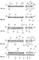
- Fig. 1a shows provided electrically conductive metal elements 10 and 10 ', each of which is used to produce spacer systems.
- the electrically conductive Metal elements 10 and 10 ' are metal elements of this type which comprise at least one layer with copper or a copper alloy.
- the electrically conductive metal elements it is possible for the electrically conductive metal elements to comprise a molybdenum-copper material and / or a tungsten-copper material and / or a copper-molybdenum-copper composite material.
- the metal element 10 has a depression 15 on the first contacting side 11.
- the metal element 10 ′ also has such a depression 15 on the first contacting side 11.
- the second contacting side 12 of the metal element 10 has no depression.
- the metal element 10 ' has a further depression 15' on the second contacting side 12.
- the depression 15 ′ of the second contacting side 12 is congruent with the depression 15 of the first contacting side 11.
- the depressions 15 and 15 ' are each formed by a bottom surface 16 and (inner) side edges 17.
- the metal elements 10 and 10 ' can be coated.
- the coating 20 is formed both on the contacting sides 11 and 12 and in the depressions 15 and 15 '. In connection with the depressions 15 and 15 ', this applies to both the bottom surfaces 16 and the side edges 17.
- the coating is preferably carried out as part of a galvanizing process.
- the coating 20 can, for example, provide corrosion resistance as well as an improved connection of a sintering paste to be applied later.
- a sintering paste 30 is applied to both sides 11 and 12 of the metal elements 10 and 10 '.
- the sintering paste 30 is in particular introduced into the depressions 15 and 15 '.
- the sintering paste 30 is also applied to the second contacting side 12.
- Sintering paste 30 is preferably a silver sintering paste.
- a doctor blade method can be used for application into the depressions 15 and 15 '.
- the sintering paste 30 can thus in the Depressions 15 and 15 'are coated with the aid of a doctor blade.
- the sintering paste 30 has such a material thickness that the recesses 15 and 15 'are completely filled with sintering paste 30.
- a pre-fixing means 31 is also applied to the second contacting side 12 of the metal element 10.
- the pre-fixing means 31 is, for example, an adhesive.
- the pre-fixing means 31 can be applied in the form of adhesive dots.
- the pre-fixing agent 31 is applied to the side of the sintering paste 30 on the second contacting side 12.
- Fig. 1d the metal elements 10 and 10 'are shown in a dried state. Due to the drying process, the material thickness of the sintering paste 30 decreases. Due to the reduction in thickness, cavities 40, 40 'are formed in connection with the depressions 15 and 15'. The cavities 40, 40 'are formed by the dried sintering paste 35 and the again exposed inside edges 41 of the depressions 15 and 15'.
- the pre-fixing means 31 applied in dot form are also reduced in connection with their height.
- the temporary pre-fixing agent has a greater material thickness than the dried sintering paste 35.
- Fig. 1d It is shown that the metal elements 10 and 10 ′, which comprise both dried sintering pastes 35 and a pre-fixing agent 31, are placed on a temporary carrier 45.
- the metal elements 10 and 10 'together with the temporary carrier 45 form a spacer system 100 and 110, respectively.
- the spacer systems 100 and 110 can be transported to a further production site or to a customer or manufacturer of Power electronics modules.
- the temporary carrier 45 is a film frame.
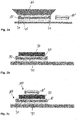
- both the spacer system 100 and the spacer system 110 are detached from the temporary carrier 45. This can be done using a nozzle 60.
- the spacer system 100 which has only one depression 15 on the first contacting side 11, is placed on a substrate 70.
- a chip 90 can then be placed in the cavity 40.
- the cavity 40 serves as an assembly aid or as a fixing aid. In the as-yet unsintered state, the chip 90 cannot slip at least laterally, so that the chip 90 is temporarily fixed in the cavity 40.
- the cavity Before the chip 90 is placed in the cavity 40, the cavity can additionally be filled with an adhesive, in particular a sintering adhesive or a polymer.
- An adhesive applied in this way can be applied, for example, by means of dispensing or jetting. This causes no voids to be formed between the chip 90 and the metal element 10.
- the chip 90 can, as shown in Fig. 2c is shown, then the spacer system 110 is placed.
- the second contacting side 12 with the recess 15 ′ formed therein is applied to the chip 90. Due to the sintering paste 35 formed in the recess 15 'and dried in the meantime, contacting, namely upper contacting, of the chip 90 can thus be carried out with the aid of the spacer system 110.
- the chip can be sintered together with the spacer systems 100 and 110 with the substrate.
- the method steps illustrated make it clear that with the aid of the spacer systems 100, 110 according to the invention and due to the use of these spacer systems 100 and 110 according to the invention, height differences between different elements of a power electronics module to be produced can be compensated in a simple manner.
Landscapes
- Engineering & Computer Science (AREA)
- Computer Hardware Design (AREA)
- Microelectronics & Electronic Packaging (AREA)
- Power Engineering (AREA)
- Manufacturing & Machinery (AREA)
- Die Bonding (AREA)
Abstract
Die Erfindung betrifft ein Verfahren zum Herstellen eines Spacer-Systems (100, 110) zur Kontaktierung mindestens eines Chips (90) mit einem Substrat (70), umfassend die Schritte:- Bereitstellen eines elektrisch leitenden Metallelements (10, 10'), das Kupfer umfasst, wobei das Metallelement (10, 10') zwei gegenüberliegend ausgebildete Kontaktierungsseiten (11, 12) aufweist,- Strukturieren des Metallelements (10, 10'), wobei zumindest auf einer ersten Kontaktierungsseite (11) eine Vertiefung (15) ausgebildet wird,- Auftragen von Sinterpaste (30) auf die mindestens erste Kontaktierungsseite (11), insbesondere auf beide Kontaktierungsseiten (11, 12), wobei die Vertiefung (15) der ersten Kontaktierungsseite (11) zumindest abschnittsweise mit Sinterpaste (30) gefüllt wird,- Trocknen der Sinterpaste (30), wobei die Materialdicke der aufgetragenen Sinterpaste (30) reduziert wird.Auf einer Kontaktierungsseite (11, 12) des Metallelements (10, 10'), insbesondere auf der zweiten Kontaktierungsseite (12), kann zumindest abschnittsweise ein temporäres Vorfixiermittel (31), insbesondere in Form von Klebepunkten, aufgebracht werden. Das Metallelement (10, 10'), das die getrocknete Sinterpaste (35) umfasst, kann auf einem temporären Träger (45) aufgebracht werden, insbesondere derart, dass die zweite Kontaktierungsseite (12) zu dem temporären Träger (45) weist.Die Erfindung betrifft auch ein entsprechendes Spacer-System (100, 110) und eine Verwendung des Spacer-Systems (100, 110) zur Kontaktierung mindestens eines Chips (90) mit einem Substrat (70), umfassend die Schritte:- Bereitstellen eines Substrats (70),- Optionales Ablösen des elektrisch leitenden Metallelements (10, 10') zusammen mit der getrockneten Sinterpaste (35) und optional ausgebildetem Vorfixiermittel (31) von dem temporären Träger (45),- Aufbringen des elektrisch leitenden Metallelements (10, 10') zusammen mit der getrockneten Sinterpaste (35) und optional ausgebildetem Vorfixiermittel (31) auf dem Substrat (70) derart, dass die zweite Kontaktierungsseite (12) zum Substrat (70) weisend positioniert ist,- Einsetzen mindestens eines Chips (90) in mindestens eine Kavität (15), die durch die Vertiefung (15) mit der getrockneten Sinterpaste (35) gebildet ist,- Sintern des Spacer-Systems (100, 110) mit dem Chip (90) und dem Substrat (70).Ein zweites Spacer-System (110) auf dem mit einem ersten Spacer-System (100) verbundenen Chip (90) kann aufgebracht und mit dem Chip (90) versintert werden.The invention relates to a method for producing a spacer system (100, 110) for contacting at least one chip (90) with a substrate (70), comprising the steps of: providing an electrically conductive metal element (10, 10 '), the copper comprises, the metal element (10, 10 ') having two oppositely formed contacting sides (11, 12), structuring of the metal element (10, 10'), a recess (15) being formed on at least one first contacting side (11), - Application of sintering paste (30) to the at least first contacting side (11), in particular to both contacting sides (11, 12), the recess (15) of the first contacting side (11) being at least partially filled with sintering paste (30), - drying the sintering paste (30), the material thickness of the applied sintering paste (30) being reduced. On a contacting side (11, 12) of the metal element (10, 10 '), in particular on the second contacting side e (12), a temporary pre-fixing agent (31), in particular in the form of adhesive dots, can be applied at least in sections. The metal element (10, 10 ') which comprises the dried sintering paste (35) can be applied to a temporary carrier (45), in particular in such a way that the second contacting side (12) faces the temporary carrier (45) also relates to a corresponding spacer system (100, 110) and a use of the spacer system (100, 110) for contacting at least one chip (90) with a substrate (70), comprising the steps: - providing a substrate (70) - Optional detachment of the electrically conductive metal element (10, 10 ') together with the dried sintering paste (35) and optionally formed prefixing agent (31) from the temporary carrier (45), - Application of the electrically conductive metal element (10, 10') together with the dried sintering paste (35) and optionally formed pre-fixing means (31) on the substrate (70) in such a way that the second contacting side (12) is positioned facing the substrate (70), - inserting at least one chip (90) in at least firstly a cavity (15) which is formed by the recess (15) with the dried sintering paste (35), - sintering the spacer system (100, 110) with the chip (90) and the substrate (70). A second The spacer system (110) can be applied to the chip (90) connected to a first spacer system (100) and sintered with the chip (90).
Description
Die Erfindung bezieht sich auf ein Verfahren zum Herstellen eines Spacer-Systems. Des Weiteren betrifft die Erfindung ein Spacer-System, das insbesondere nach einem erfindungsgemäßen Verfahren hergestellt ist. Außerdem betrifft die Erfindung die Verwendung eines Spacer-Systems. Ferner betrifft die Erfindung einen Chip, der mit mindestens einem erfindungsgemäßen Spacer-System verbunden ist.The invention relates to a method for producing a spacer system. Furthermore, the invention relates to a spacer system which is produced in particular by a method according to the invention. The invention also relates to the use of a spacer system. The invention further relates to a chip which is connected to at least one spacer system according to the invention.
Steigende Anforderungen hinsichtlich der Leistung und Lebensdauer in Leistungselektronik-Modulen erhöhen die Anforderungen an die Kontaktierung der Leistungshalbleiter sowohl auf der Oberseite als auch auf der Unterseite. Im Stand der Technik sind z.B. Aluminium-Bonddraht-Verbindungen bekannt, die jedoch hinsichtlich der Kontaktierbarkeit an ihre Grenzen stoßen.Increasing requirements with regard to performance and service life in power electronics modules increase the requirements for contacting the power semiconductors both on the top and on the bottom. In the prior art e.g. Aluminum bond wire connections are known, but they reach their limits in terms of contactability.
Weitere Lösungen hinsichtlich der Kontaktierung von Leistungshalbleitern beruhen auf umfangreichen Biegevorgängen und Strukturierungen. Dabei handelt es sich oftmals um sehr aufwändige Lösungen, die zum einen sehr teuer und zum anderen äußerst kompliziert in der Herstellung sind.Further solutions regarding the contacting of power semiconductors are based on extensive bending processes and structuring. These are often very complex solutions, which are very expensive on the one hand and extremely complicated to manufacture on the other.
Des Weiteren ist bei der Herstellung von Leistungselektronik-Modulen bei verschiedenen Chips bzw. bei der entsprechenden Verbindung/Kontaktierung von Chips und Substraten mit Höhenunterschieden zu rechnen. Dies bedingt eine entsprechende Nachbearbeitung bei der Herstellung von Leistungselektronik-Modulen. Gleiches gilt im Zusammenhang mit Unterschieden im Bereich der verschiedenen Wärmeausdehnungskoeffizienten von unterschiedlichen Materialien, die zu einem Leistungselektronik-Modul verarbeitet werden sollen.Furthermore, differences in height can be expected in the manufacture of power electronics modules for various chips or in the corresponding connection / contacting of chips and substrates. This requires a corresponding post-processing in the production of power electronics modules. The same applies in connection with differences in the range of the different coefficients of thermal expansion of different materials that are to be processed into a power electronics module.
Ausgehend von diesem Stand der Technik, ist es Aufgabe der vorliegenden Erfindung ein Verfahren zum Herstellen eines Spacer-Systems anzugeben, wobei das Verfahren einfach durchzuführen sein soll und zum anderen auf keinen aufwändigen bzw. teuren Materialien und Verfahrensschritten basieren soll.Starting from this prior art, it is the object of the present invention to specify a method for producing a spacer system, the method being intended to be simple to carry out and secondly not to be based on complex or expensive materials and method steps.
Des Weiteren ist es Aufgabe der vorliegenden Erfindung ein weiterentwickeltes Spacer-System zur Verfügung zu stellen, das als Zwischenprodukt dienen kann und für unterschiedliche Arten von Leistungselektronik-Modulen verwendet werden kann.Furthermore, it is an object of the present invention to provide a further developed spacer system which can serve as an intermediate product and can be used for different types of power electronics modules.
Ferner ist es Aufgabe der vorliegenden Erfindung eine weiterentwickelte Verwendung eines Spacer-Systems anzugeben. Außerdem ist es Aufgabe der Erfindung, einen Chip mit einem erfindungsgemäßen Spacer-System, anzugeben.Furthermore, it is an object of the present invention to provide a further developed use of a spacer system. It is also an object of the invention to provide a chip with a spacer system according to the invention.
Erfindungsgemäß wird diese Aufgabe mit Blick auf das Verfahren zum Herstellen eines Spacer-Systems durch den Gegenstand des Anspruches 1, mit Blick auf das Spacer-System zur Kontaktierung mindestens eines Chips mit einem Substrat, durch den Gegenstand des Anspruches 6, mit Blick auf die Verwendung eines Spacer-Systems zur Kontaktierung mindestens eines Chips mit einem Substrat durch den Gegenstand des Anspruches 12 und mit Blick auf den Chip durch den Gegenstand des Anspruches 14 gelöst.According to the invention, this object is achieved with a view to the method for producing a spacer system by the subject matter of
Die Erfindung beruht auf dem Gedanken, ein Verfahren zum Herstellen eines Spacer-Systems zur Kontaktierung mindestens eines Chips mit einem Substrat anzugeben, das folgende Schritte umfasst:
- Bereitstellen eines elektrisch leitenden Metallelements, das Kupfer umfasst, wobei das Metallelement zwei gegenüberliegend ausgebildete Kontaktierungsseiten aufweist,
- Strukturieren des Metallelements, wobei zumindest auf einer ersten Kontaktierungsseite eine Vertiefung ausgebildet wird,
- Auftragen von Sinterpaste auf die mindestens erste Kontaktierungsseite, vorzugsweise auf beide Kontaktierungsseiten, wobei die Vertiefung der ersten Kontaktierungsseite zumindest abschnittsweise mit Sinterpaste gefüllt wird,
- Trocknen der Sinterpaste, wobei die Materialdicke der aufgetragenen Sinterpaste reduziert wird.
- Providing an electrically conductive metal element comprising copper, the metal element having two contacting sides formed opposite one another,
- Structuring the metal element, a recess being formed at least on a first contacting side,
- Applying sintering paste to the at least first contacting side, preferably to both contacting sides, the recess of the first contacting side being filled with sintering paste at least in sections,
- Drying the sintering paste, the material thickness of the applied sintering paste being reduced.
Das mit Hilfe des erfindungsgemäßen Verfahrens hergestellte Spacer-System dient zur nachfolgenden Kontaktierung mindestens eines Chips mit einem Substrat.The spacer system produced with the aid of the method according to the invention is used for the subsequent contacting of at least one chip with a substrate.
Das elektrisch leitende Metallelement kann in Form einer Metallfolie oder eines Metallbandes, insbesondere in Form eines Metallfolienabschnittes oder in Form eines Metallbandabschnittes, vorliegen. Das elektrisch leitende Metallelement umfasst dabei Kupfer. Es ist möglich, dass das elektrisch leitende Element zumindest eine Schicht aus reinem Kupfer umfasst. Des Weiteren ist es möglich, dass das elektrisch leitende Metallelement mehrere Schichten umfasst, wobei wenigstens eine Schicht Kupfer umfasst und/oder aus Kupfer besteht.The electrically conductive metal element can be in the form of a metal foil or a metal strip, in particular in the form of a metal foil section or in the form of a metal strip section. The electrically conductive metal element comprises copper. It is possible for the electrically conductive element to comprise at least one layer of pure copper. Furthermore, it is possible for the electrically conductive metal element to comprise a plurality of layers, at least one layer comprising copper and / or consisting of copper.
Nach dem Bereitstellen des elektrisch leitenden Metallelementes folgt das Strukturieren des Metallelements, wobei zumindest auf einer ersten Kontaktierungsseite eine Vertiefung ausgebildet wird. Es ist auch möglich, dass auf beiden Kontaktierungsseiten bzw. auf den zwei gegenüberliegenden Kontaktierungsseiten des Metallelements mindestens jeweils eine Vertiefung eingebracht wird. Als Vertiefung ist insbesondere eine derartige Struktur zu verstehen, die keinen vollständigen Durchbruch bzw. kein Loch bildet. Vielmehr handelt es sich bei einer Vertiefung um eine derartige Struktur, die eine Bodenfläche mit Seitenflächen aufweist. Die Vertiefung kann dabei unterschiedliche Formen aufweisen. Die Grundfläche der Vertiefung, d.h. die Bodenfläche der Vertiefung kann dabei eine längliche Form aufweisen. Insbesondere weist die Bodenfläche der Vertiefung eine quadratische oder rechteckige Form auf.After the provision of the electrically conductive metal element, the metal element is structured, a recess being formed at least on a first contacting side. It is also possible for at least one depression to be made on each of the two contacting sides or on the two opposite contacting sides of the metal element. A depression is to be understood in particular as a structure of this type which does not form a complete breakthrough or a hole. Rather, a depression is such a structure that has a bottom surface with side surfaces. The deepening can have different shapes. The base of the depression, ie the bottom surface of the depression, can have an elongated shape. In particular, the bottom surface of the depression has a square or rectangular shape.
In einer weiteren Ausführungsform der Erfindung ist es möglich, dass auf beiden Seiten des Metallelements, d.h. auf beiden Kontaktierungsseiten, mindestens jeweils eine Vertiefung eingebracht wird, wobei die Vertiefungen in einem derartigen Fall vorzugsweise die gleichen Grundformen aufweisen. Dies erleichtert den Herstellungsprozess. In einer besonderes bevorzugten Ausführungsform der Erfindung sind die Vertiefungen deckungsgleich angeordnet.In a further embodiment of the invention it is possible that on both sides of the metal element, i.e. on both contacting sides, at least one depression is made in each case, the depressions preferably having the same basic shapes in such a case. This simplifies the manufacturing process. In a particularly preferred embodiment of the invention, the depressions are arranged congruently.
Ein Schritt des erfindungsgemäßen Verfahrens umfasst das Auftragen von Sinterpaste mindestens auf die erste Kontaktierungsseite, vorzugsweise auf beiden Kontaktierungsseiten, wobei die in einem vorangegangenen Verfahrensschritt eingearbeitete Vertiefung mit der Sinterpaste gefüllt wird. Es ist möglich, dass zusätzliche Flächen des Metallelements, insbesondere die weitere Kontaktierungsseite, die möglicherweise keine Vertiefung aufweist, ebenfalls mit Sinterpaste versehen wird bzw. dort entsprechende Sinterpaste aufgetragen wird.One step of the method according to the invention comprises the application of sintering paste at least on the first contacting side, preferably on both contacting sides, the recess incorporated in a previous method step being filled with the sintering paste. It is possible that additional surfaces of the metal element, in particular the further contacting side, which may not have a depression, are also provided with sintering paste or corresponding sintering paste is applied there.
Die Vertiefung der ersten Kontaktierungsseite wird zumindest abschnittsweise mit Sinterpaste gefüllt. Das bedeutet, dass keine vollständige Füllung der gesamten Vertiefung mit Sinterpaste erfolgt. Vorzugsweise wird die Sinterpaste in die mindestens eine Vertiefung derart eingebracht, dass die vollständige Bodenfläche der Vertiefung mit Sinterpaste beschichtet ist. Die Vertiefung muss jedoch nicht zwangsläufig vollständig, d.h. über ihre gesamte Tiefe hinweg mit Sinterpaste gefüllt sein.The recess of the first contacting side is filled with sintering paste at least in sections. This means that the entire recess is not completely filled with sintering paste. The sintering paste is preferably introduced into the at least one depression in such a way that the entire bottom surface of the depression is coated with sintering paste. However, the deepening does not necessarily have to be complete, i.e. be filled with sinter paste over their entire depth.
In Abhängigkeit der zu verwendenden Sinterpaste kann es jedoch vorgesehen sein, dass die Vertiefung vollständig mit Sinterpaste gefüllt wird oder die Sinterpaste derart aufgetragen wird, dass die in die Vertiefung eingebrachte Sinterpaste über den Vertiefungsrand hinweg vorsteht. Mit anderen Worten kann die Sinterpaste über die erste Kontaktierungsseite auch im Bereich der Vertiefung überstehen. In einem nachfolgenden Trocknungsschritt wird die Materialdicke der aufgetragenen Sinterpaste entsprechend reduziert. Die Trocknung der Sinterpaste erfolgt vorzugsweise derart, dass die Vertiefung mit der aufgetragenen und getrockneten Sinterpaste wiederum seitliche Randbereiche der Vertiefung freigibt, so dass die Vertiefung mit der aufgebrachten und getrockneten Sinterpaste selbst eine Kavität bildet.Depending on the sintering paste to be used, however, it can be provided that the depression is completely filled with sintering paste or the sintering paste is applied in such a way that the sintering paste introduced into the depression protrudes beyond the depression edge. In other words, the sintering paste can also protrude beyond the first contacting side in the region of the depression. In a subsequent drying step, the material thickness of the sintering paste applied is reduced accordingly. The sintering paste is preferably dried in such a way that the depression with the applied and dried sinter paste in turn releases lateral edge areas of the depression, so that the depression itself forms a cavity with the applied and dried sinter paste.
Aufgrund der zumindest abschnittsweise in einer Vertiefung befindlichen Sinterpaste kann eine Kavität gebildet werden, die eine spätere Platzierung eines Chips vereinfacht.Due to the sintering paste located at least in sections in a depression, a cavity can be formed which simplifies later placement of a chip.
Es ist möglich, dass das strukturierte Metallelement vor dem Auftragen von Sinterpaste metallisiert, insbesondere galvanisiert, wird.It is possible that the structured metal element is metallized, in particular galvanized, before the sintering paste is applied.
In einer weiteren Ausführungsform des erfindungsgemäßen Verfahrens ist es möglich, dass auf einer Kontaktierungsseite, insbesondere auf der zweiten Kontaktierungsseite, zumindest abschnittsweise ein temporäres Vorfixiermittel aufgebracht wird. Das temporäre Vorfixiermittel wird insbesondere auf der Kontaktierungsseite des Metallelements aufgebracht, die keine mit Sinterpaste gefüllte Vertiefung aufweist.In a further embodiment of the method according to the invention, it is possible for a temporary pre-fixing agent to be applied to a contacting side, in particular on the second contacting side, at least in sections. The temporary pre-fixing agent is applied in particular to the contacting side of the metal element, which has no recess filled with sintering paste.
Es ist möglich, dass das Metallelement, das getrocknete Sinterpaste umfasst, auf einem temporären Träger aufgebracht wird. Insbesondere handelt es sich bei dem Metallelement in diesem Fall um mehrere zusammenhängende Metallelementteile, die auf dem Träger liegend vereinzelt werden können. Es ist auch möglich, dass ein bereits vereinzeltes Metallelement auf einem temporären Träger aufgebracht oder platziert wird.It is possible that the metal element, which comprises dried sintering paste, is applied to a temporary carrier. In particular, the metal element in this case is a plurality of coherent metal element parts which can be separated lying on the carrier. It is also possible for an already isolated metal element to be applied or placed on a temporary support.
In einer besonders bevorzugten Ausführungsform der Erfindung wird das Metallelement mit der getrockneten Sinterpaste derart auf den temporären Träger aufgebracht, dass die zweite Kontaktierungsseite zu dem temporären Träger weist. Bei der zweiten Kontaktierungsseite handelt es sich folglich um die Seite des Metallelements, das optional keine Vertiefung jedoch möglicherweise ein temporäres Vorfixiermittel aufweist.In a particularly preferred embodiment of the invention, the metal element with the dried sintering paste is applied to the temporary carrier in such a way that the second contacting side faces the temporary carrier. The second contacting side is consequently the side of the metal element, which optionally has no depression, but possibly has a temporary pre-fixing agent.
Bei dem temporären Träger kann es sich um einen Wafer-Frame oder um einen Teil eines Wafer-Frames handeln. Dieser Wafer-Frame weist vorzugsweise eine spezielle Folie auf. Im Rahmen eines Pick-and-Place-Prozesses kann das strukturierte Metallelement wieder von dem temporären Träger abgenommen werden. Das Zwischenprodukt kann unter Umständen bereits mit einem Chip versehen sein. Der Chip ist dabei auf dem Sintermaterial aufgebracht, das zumindest abschnittsweise in der Vertiefung ausgebildet ist.The temporary carrier can be a wafer frame or part of a wafer frame. This wafer frame preferably has a special film. As part of a pick-and-place process, the structured metal element can be removed from the temporary carrier again become. Under certain circumstances, the intermediate product can already be provided with a chip. The chip is applied to the sintered material, which is formed at least in sections in the depression.
Des Weiteren ist es möglich, dass ein Metallelement, das getrocknete Sinterpaste aufweist, in einem Waffle Pack verpackt und transportiert wird.Furthermore, it is possible for a metal element which has dried sintering paste to be packaged and transported in a waffle pack.
Insgesamt ist zu erkennen, dass das erfindungsgemäße Verfahren zum Herstellen eines Spacer-Systems zur Kontaktierung mindestens eines Chips mit einem Substrat äußerst einfach ausgeführt werden kann. Das erfindungsgemäße Verfahren ist für eine Vielzahl von unterschiedlichen Spacer-Systemen geeignet.Overall, it can be seen that the method according to the invention for producing a spacer system for contacting at least one chip with a substrate can be carried out extremely simply. The method according to the invention is suitable for a large number of different spacer systems.
Gemäß einem weiteren, insbesondere nebengeordneten, Aspekt der Erfindung wird ein Spacer-System zur Kontaktierung mindestens eines Chips mit einem Substrat angegeben. Insbesondere handelt es sich dabei um ein erfindungsgemäß hergestelltes Spacer-System.According to a further, in particular secondary aspect of the invention, a spacer system for contacting at least one chip with a substrate is specified. In particular, it is a spacer system produced according to the invention.
Bei einem Spacer-System handelt es sich mit anderen Worten um ein Abstandshalter-System. Das Spacer-System umfasst ein elektrisch leitendes Metallelement, das Kupfer umfasst und zwei gegenüberliegend ausgebildete Kontaktierungsseiten aufweist, wobei auf mindestens einer ersten Kontaktierungsseite eine Vertiefung ausgebildet ist und auf beiden Kontaktierungsseiten getrocknete Sinterpaste ausgebildet ist.In other words, a spacer system is a spacer system. The spacer system comprises an electrically conductive metal element which comprises copper and has two contacting sides formed opposite one another, a recess being formed on at least one first contacting side and dried sintering paste being formed on both contacting sides.
Die Vertiefung ist abschnittsweise mit getrockneter Sinterpaste gefüllt, derart, dass die Vertiefung mit der getrockneten Sinterpaste eine Kavität bildet, wobei das Spacer-System auf einem temporären Träger aufgebracht ist. Hinsichtlich des Spacer-Systems gelten die bereits im Zusammenhang mit dem erfindungsgemäßen Verfahren angegebenen Erläuterungen.The recess is partially filled with dried sintering paste in such a way that the recess forms a cavity with the dried sintering paste, the spacer system being applied to a temporary carrier. With regard to the spacer system, the explanations already given in connection with the method according to the invention apply.
Das elektrisch leitende Metallelement umfasst zumindest eine Schicht mit Kupfer oder einer Kupferlegierung. Mit anderen Worten weist mindestens eine Schicht des elektrisch leitenden Metallelements ein Kupfermaterial auf. Des Weiteren kann das elektrisch leitende Metallelement ein Molybdän-Kupfer-Material (MoCu) und/oder ein Wolfram-Kupfer-Material (WCu) und/oder ein Kupfer-Molybdän-Kupfer-Verbundwerkstoff (CuMoCu) sein.The electrically conductive metal element comprises at least one layer with copper or a copper alloy. In other words, at least one layer of the electrically conductive metal element has a copper material. Furthermore, the electrically conductive metal element can be a molybdenum-copper material (MoCu) and / or a tungsten-copper material (WCu) and / or a copper-molybdenum-copper composite material (CuMoCu).
Bei der Sinterpaste handelt es sich vorzugsweise um eine Silbersinterpaste. Die getrocknete Silbersinterpaste weist vorzugsweise eine Rest-Reaktivität auf, derart, dass die bereits aufgebrachte und getrocknete, insbesondere vorgetrocknete, Silbersinterpaste bei Durchführen eines nachfolgenden Sinterprozesses eine entsprechende Verbindung zu einem Chip und/oder einem Substrat herstellen kann.The sintering paste is preferably a silver sintering paste. The dried silver sintering paste preferably has a residual reactivity such that the already applied and dried, in particular pre-dried, silver sintering paste can produce a corresponding connection to a chip and / or a substrate when a subsequent sintering process is carried out.
Auf der zweiten Kontaktierungsseite ist vorzugsweise zumindest abschnittsweise ein temporäres Vorfixiermittel, insbesondere in Form von Klebepunkten, ausgebildet.A temporary pre-fixing means, in particular in the form of adhesive dots, is preferably formed on the second contacting side, at least in sections.
Bei dem Vorfixiermittel kann es sich beispielsweise um einen Klebstoff handeln. Des Weiteren ist es möglich, dass es sich bei dem Vorfixiermittel um einen druckaktivierbaren Klebstoff handelt.The pre-fixing agent can, for example, be an adhesive. Furthermore, it is possible that the pre-fixing agent is a pressure-activatable adhesive.
Außerdem ist es möglich, dass das Vorfixiermittel flächig, beispielsweise streifenförmig, auf mindestens eine Kontaktierungsseite, insbesondere auf die zweite Kontaktierungsseite aufgebracht wird. Vorzugsweise ist das Vorfixiermittel auf der Seite des Spacer-Systems aufgebracht, das keine Vertiefung mit darin befindlichem Sinterpasten-Material aufweist.In addition, it is possible for the prefixing agent to be applied in a flat manner, for example in the form of a strip, to at least one contacting side, in particular to the second contacting side. The prefixing agent is preferably applied to the side of the spacer system which has no recess with sintering paste material located therein.
Des Weiteren ist es bevorzugt, dass das temporäre Vorfixiermittel seitlich einer Sinterpaste auf der zweiten Kontaktierungsseite ausgebildet ist. Es ist möglich, dass ein flächiger Abschnitt, beispielsweise streifenförmig oder quadratisch oder rechteckig, der zweiten Kontaktierungsseite mit einer Sinterpaste beschichtet wird. Das temporäre Vorfixiermittel kann demnach als seitliche Umrandung dieser Sinterpaste bzw. des Sinterpastenabschnittes, ausgebildet sein. Dabei kann das temporäre Vorfixiermittel zu dem Sinterpastenabschnitt beabstandet ausgebildet sein.Furthermore, it is preferred that the temporary pre-fixing means is formed on the side of a sintering paste on the second contacting side. It is possible for a flat section, for example strip-shaped or square or rectangular, to be coated on the second contacting side with a sintering paste. The temporary pre-fixing means can accordingly be designed as a lateral border of this sintering paste or of the sintering paste section. The temporary pre-fixing means can be formed at a distance from the sintering paste section.
Um eine ausreichende Vorfixierung zu ermöglichen, weist das optional ausgebildete temporäre Vorfixiermittel vorzugsweise eine größere Materialdicke als die Sinterpaste auf. Mit anderen Worten kann das temporäre Vorfixiermittel über die Sinterpaste vorstehen, so dass eine Fixierung des Metallelements an einem weiteren Bauteil, insbesondere an einem temporären Träger und/oder an einem Substrat, ermöglicht wird.In order to enable adequate pre-fixing, the optionally designed temporary pre-fixing agent preferably has a greater material thickness than the sintering paste. In other words, the temporary pre-fixing means can protrude beyond the sintering paste, so that the metal element can be fixed to a further component, in particular to a temporary carrier and / or to a substrate.
Die mindestens eine Kavität des Spacer-Systems kann durch einen getrockneten Sinterpastenabschnitt und Innenseitenkanten des Metallelements gebildet sein. Bei den Innenseitenkanten des Metallelements handelt es sich um Abschnitte der Innenseitenkanten einer in das Metallelement eingebrachten Vertiefung. Die Kavität dient folglich als Fixierabschnitt. Ein in die Kavität eingebrachtes bzw. aufgelegtes Halbleiterelement, insbesondere ein Chip, kann in einer derartigen Kavität bereits vor dem tatsächlichen Sinterschritt nicht mehr leicht verrutschen.The at least one cavity of the spacer system can be formed by a dried sintering paste section and inside edges of the metal element. The inside edges of the metal element are sections of the inside edges of a recess made in the metal element. The cavity therefore serves as a fixing section. A semiconductor element, in particular a chip, which is introduced or placed in the cavity can no longer easily slip in such a cavity even before the actual sintering step.
Aufgrund des erfindungsgemäßen Spacer-Systems können Höhenunterschiede oder herstellungstechnische Unterschiede aufgrund unterschiedlicher Wärmeausdehnungskoeffizienten der verwendeten Materialien sowohl auf einer Halbleiter- oder Chip-Oberseite als auch unter dem Halbleiterelement bzw. unter einem Chip ausgeglichen werden. Dies kann beispielsweise der Fall sein, sofern unterschiedliche Chips, wie z.B. IGBT und Dioden, oberseitig mit einem Kupfer-Leadframe kontaktiert werden, der Gate-Kontakt jedoch mit einem Wire-Bond ausgeführt wird. Ein in einem derartigen Fall verwendeter Bond-Loop weist eine gewisse Höhe auf und darf das obere Leadframe nicht berühren.Due to the spacer system according to the invention, differences in height or manufacturing differences due to different coefficients of thermal expansion of the materials used can be compensated for both on a semiconductor or chip top and under the semiconductor element or under a chip. This can be the case, for example, if different chips, e.g. IGBT and diodes are contacted on the top side with a copper lead frame, but the gate contact is carried out with a wire bond. A bond loop used in such a case has a certain height and must not touch the upper lead frame.
Das Strukturieren des Metallelements, insbesondere das Ausbilden oder Einbringen einer Vertiefung auf die erste Kontaktierungsseite des Metallelements kann insbesondere durch einen Prägevorgang durchgeführt werden.The structuring of the metal element, in particular the formation or introduction of a depression on the first contacting side of the metal element, can in particular be carried out by an embossing process.
Aufgrund der ausgebildeten Vertiefung kann die Sinterpaste in einfacher Art und Weise in die Vertiefung eingebracht werden. Beispielsweise kann die Sinterpaste in die Vertiefung mittels eines Rakelvorgangs in die Vertiefung eingebracht werden.Due to the recess formed, the sintering paste can be introduced into the recess in a simple manner. For example, the sintering paste can be introduced into the recess by means of a doctor blade process.
Vorzugsweise ist die Kavität des Spacer-Systems derart ausgebildet, d.h. die Kavität weist eine derartige Höhe auf, dass vor dem Bestücken der Kavität mit einem Chip in die Kavität ein Klebstoff, beispielsweise ein Sinter-Kleber oder ein Polymer in die Kavität eingebracht werden kann. Ein derartiger Klebstoff kann beispielsweise durch Dispensen oder Jetten in die Kavität eingebracht werden. Das Einbringen von Klebstoff in die Kavität hat den Vorteil, dass keine Hohlräume zwischen dem Chip und dem Metallelement gebildet werden. Ein abschließendes Moulden und/oder Spritzgießen und/oder Vergießen kann folglich störungsfrei erfolgen.The cavity of the spacer system is preferably designed in such a way that the cavity has such a height that an adhesive, for example a sintering adhesive or a polymer, can be introduced into the cavity before the cavity is populated with a chip. Such an adhesive can be introduced into the cavity, for example, by dispensing or jetting. The introduction of adhesive into the cavity has the advantage that no voids are formed between the chip and the metal element. A final molding and / or injection molding and / or casting can consequently take place without problems.
Ein weiterer, insbesondere nebengeordneter, Aspekt der Erfindung betrifft die Verwendung eines erfindungsgemäßen Spacer-Systems zur Kontaktierung mindestens eines Chips mit einem Substrat. Die Verwendung umfasst dabei die Schritte:
- Bereitstellen eines Substrats,
- Ablösen des elektrisch leitenden Metallelements zusammen mit der getrockneten Sinterpaste und optional ausgebildetem Vorfixiermittel von einem/dem temporären Träger,
- Aufbringen des elektrisch leitenden Metallelements zusammen mit der getrockneten Sinterpaste und optional ausgebildetem Vorfixiermittel auf dem Substrat derart, dass die zweite Kontaktierungsseite zum Substrat weisend positioniert ist,
- Einsetzen mindestens eines Chips in die mindestens eine Kavität,
- Sintern des Spacer-Systems mit dem Chip und dem Substrat.
- Providing a substrate,
- Detaching the electrically conductive metal element together with the dried sintering paste and optionally formed pre-fixing agent from a / the temporary carrier,
- Applying the electrically conductive metal element together with the dried sintering paste and optionally formed pre-fixing agent to the substrate such that the second contacting side is positioned facing the substrate,
- Inserting at least one chip into the at least one cavity,
- Sintering the spacer system with the chip and the substrate.
Die erfindungsgemäße Verwendung kann des Weiteren die Verwendung eines zweiten Spacer-Systems umfassen, wobei das zweite Spacer-System auf dem mit einem ersten Spacer-System verbundenen Chip aufgebracht wird und mit dem Chip versintert wird.The use according to the invention can further include the use of a second spacer system, the second spacer system being applied to the chip connected to a first spacer system and being sintered with the chip.
Mit Hilfe des erfindungsgemäßen Spacer-Systems oder mit Hilfe der erfindungsgemäßen Verwendung eines Spacer-Systems können Höhenunterschiede der unterschiedlichen Bauteile ausgeglichen werden. Die anschließende oberseitige Kontaktierung kann einfach und kostengünstig durch Standardbauteile hergestellt werden. Insbesondere ist es möglich, einfache Leadframes oder DCBs zur oberseitigen Kontaktierung zu verwenden.With the aid of the spacer system according to the invention or with the aid of the use of a spacer system according to the invention, height differences of the different components can be compensated for. The subsequent top-side contacting can be produced simply and inexpensively using standard components. In particular, it is possible to use simple lead frames or DCBs for top-side contacting.
Mit Hilfe des Spacer-Systems kann außerdem zusätzlicher Raum für Bonddraht-Verbindungen hergestellt werden. Derartige Bonddraht-Verbindungen sind insbesondere zur Gate-Kontaktierung möglich.The spacer system can also be used to create additional space for bond wire connections. Bond wire connections of this type are possible in particular for gate contacting.
Des Weiteren kann der CTE (coefficient of thermal expansion) bzw. der Ausdehnungskoeffizient durch entsprechende Materialauswahl angepasst werden. Außerdem hat das Spacer-System als Zwischenprodukt den Vorteil, dass dieses von einem Leistungselektronik-Modul-Hersteller direkt vom Träger abgenommen und entsprechend weiterverarbeitet werden kann. Dies kann insbesondere zeitgleich mit einem Die Attach erfolgen.Furthermore, the CTE (coefficient of thermal expansion) or the expansion coefficient can be adjusted by appropriate material selection. In addition, the spacer system as an intermediate product has the advantage that it can be removed directly from the carrier by a power electronics module manufacturer and further processed accordingly. This can be done at the same time as a die attach.
Ein weiterer Aspekt der Erfindung betrifft einen Chip, der mit einem erfindungsgemäßen Spacer-System verbunden ist. Der Chip ist in einer Kavität des Spacer-Systems befindlich und mittels der Sinterpaste und optional weiteren Fixiermitteln mit dem Spacer-System verbunden.Another aspect of the invention relates to a chip which is connected to a spacer system according to the invention. The chip is located in a cavity of the spacer system and is connected to the spacer system by means of the sintering paste and optionally further fixing means.
Des Weiteren ist es möglich, dass ein Chip mit zwei erfindungsgemäßen Spacer-Systemen verbunden ist oder in Verbindung steht. Mit anderen Worten ist in einem derartigen Fall vorzugsweise jede Chip-Kontaktierungsseite mit einem erfindungsgemäßen Spacer-System verbunden.Furthermore, it is possible for a chip to be connected or connected to two spacer systems according to the invention. In other words, in such a case, preferably each chip contacting side is connected to a spacer system according to the invention.
Die Kavität bildet eine Fixierhilfe und/oder eine Bestückungshilfe. Insbesondere im Zusammenhang mit automatisierten Bestückungsvorgängen kann eine Kavität auch als Bestückungshilfe dienen. Eine derartige Kavität kann von optischen Erfassungssystemen einfach detektiert werden. Dies kann beispielsweise mittels eines Laserscanners erfolgen.The cavity forms a fixing aid and / or an assembly aid. In particular in connection with automated assembly processes, a cavity can also serve as an assembly aid. Such a cavity can be easily detected by optical detection systems. This can be done using a laser scanner, for example.
Nachfolgend wird die Erfindung anhand von Ausführungsbeispielen unter Bezug auf die beigefügten Zeichnungen näher erläutert.The invention is explained in more detail below on the basis of exemplary embodiments with reference to the accompanying drawings.
In diesen zeigen:
- Fig. 1a-1e
- einzelne Schritte eines erfindungsgemäßen Verfahrens zum Herstellen eines Spacer-Systems; und
- Fig. 2a-2c
- einzelne Schritte einer erfindungsgemäßen Verwendung eines erfindungsgemäßen Spacer-Systems.
- 1a-1e
- individual steps of a method according to the invention for producing a spacer system; and
- 2a-2c
- individual steps of an inventive use of a spacer system according to the invention.
Beide Metallelemente 10 und 10' weisen jeweils eine erste Kontaktierungsseite 11 und eine zweite Kontaktierungsseite 12 auf. Das Metallelement 10 weist auf der ersten Kontaktierungsseite 11 eine Vertiefung 15 auf. Auch das Metallelement 10' weist eine derartige Vertiefung 15 auf der ersten Kontaktierungsseite 11 auf. Die zweite Kontaktierungsseite 12 des Metallelements 10 weist hingegen keine Vertiefung auf.Both
Das Metallelement 10' weist auf der zweiten Kontaktierungsseite 12 eine weitere Vertiefung 15' auf. Die Vertiefung 15' der zweiten Kontaktierungsseite 12 ist deckungsgleich zur Vertiefung 15 der ersten Kontaktierungsseite 11 ausgebildet. Die Vertiefungen 15 und 15' werden jeweils von einer Bodenfläche 16 und (Innen)Seitenkanten 17 gebildet.The metal element 10 'has a further depression 15' on the second contacting
Wie in
In
Zum Auftragen in die Vertiefungen 15 und 15' kann beispielsweise ein Rakelverfahren angewendet werden. Die Sinterpaste 30 kann folglich in die Vertiefungen 15 und 15' mit Hilfe eines Rakels eingestrichen werden. Im zunächst lediglich aufgetragenen bzw. eingefüllten Zustand der Sinterpaste 30 weist die Sinterpaste 30 eine derartige Materialdicke auf, so dass die Vertiefungen 15 und 15' vollständig mit Sinterpaste 30 befüllt sind.For example, a doctor blade method can be used for application into the
Auf der zweiten Kontaktierungsseite 12 des Metallelements 10 ist außerdem ein Vorfixiermittel 31 aufgebracht. Das Vorfixiermittel 31 ist beispielsweise ein Klebemittel. Das Vorfixiermittel 31 kann in Form von Klebepunkten aufgebracht sein. Insbesondere ist das Vorfixiermittel 31 seitlich der Sinterpaste 30 auf der zweiten Kontaktierungsseite 12 aufgebracht.A pre-fixing means 31 is also applied to the second contacting
In
Aufgrund des Trocknungsprozesses werden auch die in Punktform aufgetragenen Vorfixiermittel 31 im Zusammenhang mit ihrer Höhe verringert. Allerdings weist das temporäre Vorfixiermittel auch in getrocknetem Zustand eine größere Materialdicke auf als die getrocknete Sinterpaste 35.Due to the drying process, the pre-fixing means 31 applied in dot form are also reduced in connection with their height. However, even in the dried state, the temporary pre-fixing agent has a greater material thickness than the dried
In
In den
Zunächst wird das Spacer-System 100, das lediglich eine Vertiefung 15 auf der ersten Kontaktierungsseite 11 aufweist auf einem Substrat 70 platziert. In die Kavität 40 kann anschließend ein Chip 90 gesetzt werden. Die Kavität 40 dient als Bestückhilfe oder als Fixierhilfe. Im noch unversinterten Zustand kann der Chip 90 zumindest seitlich nicht verrutschen, so dass eine temporäre Fixierung des Chips 90 in der Kavität 40 erfolgt.First, the
Vor dem Aufsetzen des Chips 90 in die Kavität 40 kann die Kavität außerdem zusätzlich mit einem Kleber, insbesondere einem Sinter-Kleber oder einem Polymer, aufgefüllt werden. Ein derart aufgebrachtes Klebemittel kann beispielsweise mittels Dispensen oder Jetten aufgebracht werden. Dies bewirkt, dass keine Hohlräume zwischen dem Chip 90 und dem Metallelement 10 gebildet werden.Before the
Auf den Chip 90 kann, wie dies in
In der in
Die Erfindung ist nicht durch die Beschreibung anhand der Ausführungsbeispiele auf diese beschränkt. Vielmehr umfasst die Erfindung jedes neue Merkmal sowie die Kombination von Merkmalen, wobei dies insbesondere jede Kombination von Merkmalen der Ansprüche beinhaltet, auch wenn dieses Merkmal oder diese Kombination selbst nicht explizit in den Ansprüchen oder Ausführungsbeispielen angegeben ist.The invention is not restricted to the exemplary embodiments by the description based on these. Rather, the invention encompasses every new feature and the combination of features, this particularly including any combination of features of the claims, even if this feature or these Combination itself is not explicitly specified in the claims or exemplary embodiments.
- 10, 10'10, 10 '
- MetallelementMetal element
- 1111
- Erste KontaktierungsseiteFirst contact page
- 1212th
- Zweite KontaktierungsseiteSecond contact page
- 15, 15'15, 15 '
- Vertiefungdeepening
- 1616
- BodenflächeFloor area
- 1717th
- SeitenkanteSide edge
- 2020
- BeschichtungCoating
- 3030th
- SinterpasteSintering paste
- 3131
- VorfixiermittelPre-fixative
- 3535
- Getrocknete SinterpasteDried sinter paste
- 4040
- Kavitätcavity
- 4141
- InnenseitenkanteInside edge
- 4545
- Temporärer TrägerTemporary carrier
- 6060
- Düsejet
- 7070
- SubstratSubstrate
- 9090
- Chipchip
- 100100
- Spacer-SystemSpacer system
- 110110
- Spacer-SystemSpacer system
Claims (14)
dadurch gekennzeichnet, dass
das strukturierte Metallelement (10, 10') vor dem Auftragen von Sinterpaste (30) metallisiert, insbesondere galvanisiert, wird.Method according to claim 1,
characterized in that
the structured metal element (10, 10 ') is metallized, in particular galvanized, before the application of sintering paste (30).
dadurch gekennzeichnet, dass
auf einer Kontaktierungsseite (11, 12), insbesondere auf der zweiten Kontaktierungsseite (12), zumindest abschnittsweise ein temporäres Vorfixiermittel (31) aufgebracht wird.Method according to claim 1 or 2,
characterized in that
on a contacting side (11, 12), in particular on the second contacting side (12), a temporary pre-fixing means (31) is applied at least in sections.
dadurch gekennzeichnet, dass
das Metallelement (10, 10'), das getrocknete Sinterpaste (35) umfasst, auf einem temporären Träger (45) aufgebracht wird.Method according to one of claims 1 to 3,
characterized in that
the metal element (10, 10 '), which comprises dried sintering paste (35), is applied to a temporary carrier (45).
dadurch gekennzeichnet, dass
das Metallelement (10, 10') derart auf dem temporären Träger (45) aufgebracht wird, dass die zweite Kontaktierungsseite (12) zu dem temporären Träger (45) weist.Method according to claim 4,
characterized in that
the metal element (10, 10 ') is applied to the temporary carrier (45) such that the second contacting side (12) faces the temporary carrier (45).
umfassend ein elektrisch leitendes Metallelement (10, 10'), das Kupfer umfasst und zwei gegenüberliegend ausgebildete Kontaktierungsseiten (11, 12) aufweist,
wobei auf mindestens einer ersten Kontaktierungsseite (11) eine Vertiefung (15) ausgebildet ist und mindestens auf der ersten Kontaktierungsseite (11), vorzugsweise auf beiden Kontaktierungsseiten (11, 12), getrocknete Sinterpaste (35) ausgebildet ist,
wobei die Vertiefung (15) abschnittsweise mit getrockneter Sinterpaste (35) gefüllt ist, derart, dass die Vertiefung (15) mit der getrockneten Sinterpaste (35) eine Kavität (40) bildet,
wobei das Spacer-System (100, 110) vorzugsweise auf einem temporären Träger (45) aufgebracht ist.Spacer system (100, 110) for contacting at least one chip (90) with a substrate (70), in particular produced by a method according to one of claims 1 to 5,
comprising an electrically conductive metal element (10, 10 ') which comprises copper and has two contacting sides (11, 12) formed opposite one another,
wherein a recess (15) is formed on at least one first contacting side (11) and dried sintered paste (35) is formed on at least the first contacting side (11), preferably on both contacting sides (11, 12),
the recess (15) being partially filled with dried sintering paste (35), such that the recess (15) forms a cavity (40) with the dried sintering paste (35),
the spacer system (100, 110) preferably on a temporary Carrier (45) is applied.
dadurch gekennzeichnet, dass
das elektrisch leitende Metallelement (10, 10') zumindest eine Schicht mit Kupfer oder einer Kupferlegierung umfasst und/oder ein Molybdän-Kupfer-Material (MoCu) ist und/oder ein Wolfram-Kupfer-Material (WCu) ist und/oder ein Kupfer-Molybdän-Kupfer-Verbundwerkstoff (CuMoCu) ist.Spacer system (100, 110) according to claim 6,
characterized in that
the electrically conductive metal element (10, 10 ') comprises at least one layer with copper or a copper alloy and / or is a molybdenum-copper material (MoCu) and / or is a tungsten-copper material (WCu) and / or a copper -Molybdenum-copper composite (CuMoCu) is.
dadurch gekennzeichnet, dass
die getrocknete Sinterpaste (35) eine Silbersinterpaste ist.Spacer system (100, 110) according to claim 6 or 7,
characterized in that
the dried sintering paste (35) is a silver sintering paste.
dadurch gekennzeichnet, dass
auf der zweiten Kontaktierungsseite (12) zumindest abschnittsweise ein temporäres Vorfixiermittel (31), insbesondere in Form von Klebepunkten, ausgebildet ist.Spacer system (100, 110) according to one of claims 6 to 8,
characterized in that
A temporary pre-fixing means (31), in particular in the form of adhesive dots, is formed on the second contacting side (12) at least in sections.
dadurch gekennzeichnet, dass
das temporäre Vorfixiermittel (31) seitlich einer/der getrockneten Sinterpaste (35) auf der zweiten Kontaktierungsseite (12) ausgebildet ist und vorzugsweise eine größere Materialdicke als die Sinterpaste (35) aufweist.Spacer system (100, 110) according to claim 9,
characterized in that
the temporary pre-fixing means (31) is formed on the side of a / the dried sintering paste (35) on the second contacting side (12) and preferably has a greater material thickness than the sintering paste (35).
dadurch gekennzeichnet, dass
die mindestens eine Kavität (40) durch einen getrockneten Sinterpastenabschnitt (35) und Innenseitenkanten (41) des Metallelements (10, 10') gebildet ist.Spacer system (100, 110) according to one of claims 6 to 10,
characterized in that
the at least one cavity (40) is formed by a dried sintering paste section (35) and inside edges (41) of the metal element (10, 10 ').
dadurch gekennzeichnet, dass
ein zweites Spacer-System (110) auf dem mit einem ersten Spacer-System (100) verbundenen Chip (90) aufgebracht wird und mit dem Chip (90) versintert wird.Use according to claim 12,
characterized in that
a second spacer system (110) is applied to the chip (90) connected to a first spacer system (100) and is sintered with the chip (90).
Priority Applications (2)
| Application Number | Priority Date | Filing Date | Title |
|---|---|---|---|
| EP19154256.2A EP3690936A1 (en) | 2019-01-29 | 2019-01-29 | Method for manufacturing a spacer system with a chip recess, corresponding spacer system and its use for contacting a chip with a substrate by sintering |
| JP2020012668A JP7049376B2 (en) | 2019-01-29 | 2020-01-29 | How to make a spacer system, spacer system, use of spacer system and tip |
Applications Claiming Priority (1)
| Application Number | Priority Date | Filing Date | Title |
|---|---|---|---|
| EP19154256.2A EP3690936A1 (en) | 2019-01-29 | 2019-01-29 | Method for manufacturing a spacer system with a chip recess, corresponding spacer system and its use for contacting a chip with a substrate by sintering |
Publications (1)
| Publication Number | Publication Date |
|---|---|
| EP3690936A1 true EP3690936A1 (en) | 2020-08-05 |
Family
ID=65268747
Family Applications (1)
| Application Number | Title | Priority Date | Filing Date |
|---|---|---|---|
| EP19154256.2A Pending EP3690936A1 (en) | 2019-01-29 | 2019-01-29 | Method for manufacturing a spacer system with a chip recess, corresponding spacer system and its use for contacting a chip with a substrate by sintering |
Country Status (2)
| Country | Link |
|---|---|
| EP (1) | EP3690936A1 (en) |
| JP (1) | JP7049376B2 (en) |
Citations (7)
| Publication number | Priority date | Publication date | Assignee | Title |
|---|---|---|---|---|
| JP2005072456A (en) * | 2003-08-27 | 2005-03-17 | Kyocera Corp | Electric element module |
| EP1684340A2 (en) * | 2005-01-20 | 2006-07-26 | Nissan Motor Co., Ltd. | Method of bonding a semiconductor element on a metal substrate |
| JP2009164208A (en) * | 2007-12-28 | 2009-07-23 | Mitsubishi Electric Corp | Semiconductor device and manufacturing method of semiconductor device |
| EP2498283A2 (en) * | 2011-03-10 | 2012-09-12 | SEMIKRON Elektronik GmbH & Co. KG | Method for manufacturing a power-semiconductor substrate |
| WO2013045345A2 (en) * | 2011-09-30 | 2013-04-04 | Robert Bosch Gmbh | Layer composite for connecting electronic components comprising a compensation layer, linking layers and connection layers |
| DE102014114982A1 (en) * | 2014-10-15 | 2016-04-21 | Infineon Technologies Ag | Method of forming a chip package and chip package |
| EP3086361A2 (en) * | 2015-04-02 | 2016-10-26 | Heraeus Deutschland GmbH & Co. KG | Method for producing a substrate arrangement with a prefixing means, corresponding substrate arrangement, method for connecting an electronic component with a substrate arrangement using a prefixing means formed on the electronic component and/or the substrate arrangement and an electronic component bonded with a substrate arrangement |
Family Cites Families (1)
| Publication number | Priority date | Publication date | Assignee | Title |
|---|---|---|---|---|
| DE102015107724B4 (en) * | 2015-04-02 | 2016-12-01 | Heraeus Deutschland GmbH & Co. KG | Method for producing a substrate arrangement, substrate arrangement, method for connecting an electronic component to a substrate arrangement and electronic component |
-
2019
- 2019-01-29 EP EP19154256.2A patent/EP3690936A1/en active Pending
-
2020
- 2020-01-29 JP JP2020012668A patent/JP7049376B2/en active Active
Patent Citations (7)
| Publication number | Priority date | Publication date | Assignee | Title |
|---|---|---|---|---|
| JP2005072456A (en) * | 2003-08-27 | 2005-03-17 | Kyocera Corp | Electric element module |
| EP1684340A2 (en) * | 2005-01-20 | 2006-07-26 | Nissan Motor Co., Ltd. | Method of bonding a semiconductor element on a metal substrate |
| JP2009164208A (en) * | 2007-12-28 | 2009-07-23 | Mitsubishi Electric Corp | Semiconductor device and manufacturing method of semiconductor device |
| EP2498283A2 (en) * | 2011-03-10 | 2012-09-12 | SEMIKRON Elektronik GmbH & Co. KG | Method for manufacturing a power-semiconductor substrate |
| WO2013045345A2 (en) * | 2011-09-30 | 2013-04-04 | Robert Bosch Gmbh | Layer composite for connecting electronic components comprising a compensation layer, linking layers and connection layers |
| DE102014114982A1 (en) * | 2014-10-15 | 2016-04-21 | Infineon Technologies Ag | Method of forming a chip package and chip package |
| EP3086361A2 (en) * | 2015-04-02 | 2016-10-26 | Heraeus Deutschland GmbH & Co. KG | Method for producing a substrate arrangement with a prefixing means, corresponding substrate arrangement, method for connecting an electronic component with a substrate arrangement using a prefixing means formed on the electronic component and/or the substrate arrangement and an electronic component bonded with a substrate arrangement |
Also Published As
| Publication number | Publication date |
|---|---|
| JP7049376B2 (en) | 2022-04-06 |
| JP2020123723A (en) | 2020-08-13 |
Similar Documents
| Publication | Publication Date | Title |
|---|---|---|
| DE102014213564B4 (en) | Semiconductor device and method for manufacturing the same | |
| DE102016117562B4 (en) | SEMICONDUCTOR CHIP WITH STRUCTURED SIDEWALLS AND METHOD FOR PRODUCING SAME | |
| DE102008035911B4 (en) | Method for manufacturing an integrated circuit module | |
| DE69233232T2 (en) | Electrical connector body and manufacturing method therefor | |
| DE2411259A1 (en) | INTEGRATED CIRCUIT AND METHOD FOR ITS MANUFACTURING | |
| DE69534483T2 (en) | Leadframe and semiconductor device | |
| DE10335622B4 (en) | Resin-sealed semiconductor device | |
| EP3026703B1 (en) | Method for producing a substrate adapter, substrate adapter and method for contacting a semiconductor element | |
| DE102020101098B4 (en) | Leadframe, encapsulated package with a stamped line and sawn side walls, and corresponding manufacturing process | |
| DE102012212968A1 (en) | OPTOELECTRONIC SEMICONDUCTOR COMPONENT WITH ELECTRICALLY INSULATED ELEMENT | |
| DE102012201172A1 (en) | Power semiconductor module with embossed base plate and method for producing a power semiconductor module with an embossed base plate | |
| DE102012213003A1 (en) | Attachment of a semiconductor chip in dry and pressure-assisted connection methods | |
| DE102009044060A1 (en) | Method for contacting wafer solar cell of e.g. solar cell string in solar cell module, involves arranging connectors on bonding surface of solar cell to bond connectors on bonding surface that lies opposite to bearing surface | |
| DE102013112708B4 (en) | Process for manufacturing an electronic component | |
| DE102013103351B4 (en) | ELECTRONIC MODULE | |
| DE102018130147A1 (en) | SEMICONDUCTOR DEVICE AND METHOD FOR PRODUCING A SEMICONDUCTOR DEVICE | |
| DE3884019T2 (en) | Method of manufacturing a module semiconductor power device and device made. | |
| DE69316159T2 (en) | Method for applying bumps on a semiconductor device and for connecting this device to a printed circuit board | |
| WO2015124608A1 (en) | Production of optoelectronic components | |
| EP3958302A1 (en) | Base plate for a semiconductor module and method for producing a base plate | |
| EP3690936A1 (en) | Method for manufacturing a spacer system with a chip recess, corresponding spacer system and its use for contacting a chip with a substrate by sintering | |
| DE102012108610B4 (en) | Chip module and method for manufacturing a chip module | |
| DE102012106431A1 (en) | Electronic component | |
| DE102020117766A1 (en) | Cast semiconductor package with double-sided cooling | |
| DE19931694B4 (en) | Method for producing electrical circuits or modules and electrical circuit or electrical module produced by this method |
Legal Events
| Date | Code | Title | Description |
|---|---|---|---|
| PUAI | Public reference made under article 153(3) epc to a published international application that has entered the european phase |
Free format text: ORIGINAL CODE: 0009012 |
|
| STAA | Information on the status of an ep patent application or granted ep patent |
Free format text: STATUS: THE APPLICATION HAS BEEN PUBLISHED |
|
| AK | Designated contracting states |
Kind code of ref document: A1 Designated state(s): AL AT BE BG CH CY CZ DE DK EE ES FI FR GB GR HR HU IE IS IT LI LT LU LV MC MK MT NL NO PL PT RO RS SE SI SK SM TR |
|
| AX | Request for extension of the european patent |
Extension state: BA ME |
|
| STAA | Information on the status of an ep patent application or granted ep patent |
Free format text: STATUS: REQUEST FOR EXAMINATION WAS MADE |
|
| 17P | Request for examination filed |
Effective date: 20201021 |
|
| RBV | Designated contracting states (corrected) |
Designated state(s): AL AT BE BG CH CY CZ DE DK EE ES FI FR GB GR HR HU IE IS IT LI LT LU LV MC MK MT NL NO PL PT RO RS SE SI SK SM TR |
|
| RAP3 | Party data changed (applicant data changed or rights of an application transferred) |
Owner name: HERAEUS DEUTSCHLAND GMBH & CO. KG |
|
| STAA | Information on the status of an ep patent application or granted ep patent |
Free format text: STATUS: EXAMINATION IS IN PROGRESS |
|
| 17Q | First examination report despatched |
Effective date: 20221123 |
|
| P01 | Opt-out of the competence of the unified patent court (upc) registered |
Effective date: 20230531 |
|
| RAP1 | Party data changed (applicant data changed or rights of an application transferred) |
Owner name: HERAEUS ELECTRONICS GMBH & CO. KG |