EP3084523B1 - Substrates comprising nano-patterning surfaces and methods of preparing thereof - Google Patents
Substrates comprising nano-patterning surfaces and methods of preparing thereof Download PDFInfo
- Publication number
- EP3084523B1 EP3084523B1 EP14824694.5A EP14824694A EP3084523B1 EP 3084523 B1 EP3084523 B1 EP 3084523B1 EP 14824694 A EP14824694 A EP 14824694A EP 3084523 B1 EP3084523 B1 EP 3084523B1
- Authority
- EP
- European Patent Office
- Prior art keywords
- layer
- functionalizable
- scale
- polymer
- nano
- Prior art date
- Legal status (The legal status is an assumption and is not a legal conclusion. Google has not performed a legal analysis and makes no representation as to the accuracy of the status listed.)
- Active
Links
Images


Classifications
-
- B—PERFORMING OPERATIONS; TRANSPORTING
- B32—LAYERED PRODUCTS
- B32B—LAYERED PRODUCTS, i.e. PRODUCTS BUILT-UP OF STRATA OF FLAT OR NON-FLAT, e.g. CELLULAR OR HONEYCOMB, FORM
- B32B3/00—Layered products comprising a layer with external or internal discontinuities or unevennesses, or a layer of non-planar shape; Layered products comprising a layer having particular features of form
- B32B3/26—Layered products comprising a layer with external or internal discontinuities or unevennesses, or a layer of non-planar shape; Layered products comprising a layer having particular features of form characterised by a particular shape of the outline of the cross-section of a continuous layer; characterised by a layer with cavities or internal voids ; characterised by an apertured layer
- B32B3/266—Layered products comprising a layer with external or internal discontinuities or unevennesses, or a layer of non-planar shape; Layered products comprising a layer having particular features of form characterised by a particular shape of the outline of the cross-section of a continuous layer; characterised by a layer with cavities or internal voids ; characterised by an apertured layer characterised by an apertured layer, the apertures going through the whole thickness of the layer, e.g. expanded metal, perforated layer, slit layer regular cells B32B3/12
-
- B—PERFORMING OPERATIONS; TRANSPORTING
- B01—PHYSICAL OR CHEMICAL PROCESSES OR APPARATUS IN GENERAL
- B01L—CHEMICAL OR PHYSICAL LABORATORY APPARATUS FOR GENERAL USE
- B01L3/00—Containers or dishes for laboratory use, e.g. laboratory glassware; Droppers
- B01L3/50—Containers for the purpose of retaining a material to be analysed, e.g. test tubes
- B01L3/502—Containers for the purpose of retaining a material to be analysed, e.g. test tubes with fluid transport, e.g. in multi-compartment structures
-
- B—PERFORMING OPERATIONS; TRANSPORTING
- B32—LAYERED PRODUCTS
- B32B—LAYERED PRODUCTS, i.e. PRODUCTS BUILT-UP OF STRATA OF FLAT OR NON-FLAT, e.g. CELLULAR OR HONEYCOMB, FORM
- B32B3/00—Layered products comprising a layer with external or internal discontinuities or unevennesses, or a layer of non-planar shape; Layered products comprising a layer having particular features of form
- B32B3/26—Layered products comprising a layer with external or internal discontinuities or unevennesses, or a layer of non-planar shape; Layered products comprising a layer having particular features of form characterised by a particular shape of the outline of the cross-section of a continuous layer; characterised by a layer with cavities or internal voids ; characterised by an apertured layer
- B32B3/30—Layered products comprising a layer with external or internal discontinuities or unevennesses, or a layer of non-planar shape; Layered products comprising a layer having particular features of form characterised by a particular shape of the outline of the cross-section of a continuous layer; characterised by a layer with cavities or internal voids ; characterised by an apertured layer characterised by a layer formed with recesses or projections, e.g. hollows, grooves, protuberances, ribs
-
- C—CHEMISTRY; METALLURGY
- C08—ORGANIC MACROMOLECULAR COMPOUNDS; THEIR PREPARATION OR CHEMICAL WORKING-UP; COMPOSITIONS BASED THEREON
- C08G—MACROMOLECULAR COMPOUNDS OBTAINED OTHERWISE THAN BY REACTIONS ONLY INVOLVING UNSATURATED CARBON-TO-CARBON BONDS
- C08G69/00—Macromolecular compounds obtained by reactions forming a carboxylic amide link in the main chain of the macromolecule
-
- G—PHYSICS
- G03—PHOTOGRAPHY; CINEMATOGRAPHY; ANALOGOUS TECHNIQUES USING WAVES OTHER THAN OPTICAL WAVES; ELECTROGRAPHY; HOLOGRAPHY
- G03F—PHOTOMECHANICAL PRODUCTION OF TEXTURED OR PATTERNED SURFACES, e.g. FOR PRINTING, FOR PROCESSING OF SEMICONDUCTOR DEVICES; MATERIALS THEREFOR; ORIGINALS THEREFOR; APPARATUS SPECIALLY ADAPTED THEREFOR
- G03F7/00—Photomechanical, e.g. photolithographic, production of textured or patterned surfaces, e.g. printing surfaces; Materials therefor, e.g. comprising photoresists; Apparatus specially adapted therefor
- G03F7/0002—Lithographic processes using patterning methods other than those involving the exposure to radiation, e.g. by stamping
-
- B—PERFORMING OPERATIONS; TRANSPORTING
- B01—PHYSICAL OR CHEMICAL PROCESSES OR APPARATUS IN GENERAL
- B01L—CHEMICAL OR PHYSICAL LABORATORY APPARATUS FOR GENERAL USE
- B01L2300/00—Additional constructional details
- B01L2300/08—Geometry, shape and general structure
- B01L2300/0887—Laminated structure
-
- B—PERFORMING OPERATIONS; TRANSPORTING
- B01—PHYSICAL OR CHEMICAL PROCESSES OR APPARATUS IN GENERAL
- B01L—CHEMICAL OR PHYSICAL LABORATORY APPARATUS FOR GENERAL USE
- B01L2300/00—Additional constructional details
- B01L2300/08—Geometry, shape and general structure
- B01L2300/0896—Nanoscaled
-
- B—PERFORMING OPERATIONS; TRANSPORTING
- B01—PHYSICAL OR CHEMICAL PROCESSES OR APPARATUS IN GENERAL
- B01L—CHEMICAL OR PHYSICAL LABORATORY APPARATUS FOR GENERAL USE
- B01L2300/00—Additional constructional details
- B01L2300/16—Surface properties and coatings
- B01L2300/161—Control and use of surface tension forces, e.g. hydrophobic, hydrophilic
- B01L2300/163—Biocompatibility
-
- B—PERFORMING OPERATIONS; TRANSPORTING
- B29—WORKING OF PLASTICS; WORKING OF SUBSTANCES IN A PLASTIC STATE IN GENERAL
- B29C—SHAPING OR JOINING OF PLASTICS; SHAPING OF MATERIAL IN A PLASTIC STATE, NOT OTHERWISE PROVIDED FOR; AFTER-TREATMENT OF THE SHAPED PRODUCTS, e.g. REPAIRING
- B29C59/00—Surface shaping of articles, e.g. embossing; Apparatus therefor
- B29C59/005—Surface shaping of articles, e.g. embossing; Apparatus therefor characterised by the choice of material
-
- B—PERFORMING OPERATIONS; TRANSPORTING
- B29—WORKING OF PLASTICS; WORKING OF SUBSTANCES IN A PLASTIC STATE IN GENERAL
- B29C—SHAPING OR JOINING OF PLASTICS; SHAPING OF MATERIAL IN A PLASTIC STATE, NOT OTHERWISE PROVIDED FOR; AFTER-TREATMENT OF THE SHAPED PRODUCTS, e.g. REPAIRING
- B29C59/00—Surface shaping of articles, e.g. embossing; Apparatus therefor
- B29C59/02—Surface shaping of articles, e.g. embossing; Apparatus therefor by mechanical means, e.g. pressing
- B29C59/022—Surface shaping of articles, e.g. embossing; Apparatus therefor by mechanical means, e.g. pressing characterised by the disposition or the configuration, e.g. dimensions, of the embossments or the shaping tools therefor
-
- B—PERFORMING OPERATIONS; TRANSPORTING
- B29—WORKING OF PLASTICS; WORKING OF SUBSTANCES IN A PLASTIC STATE IN GENERAL
- B29K—INDEXING SCHEME ASSOCIATED WITH SUBCLASSES B29B, B29C OR B29D, RELATING TO MOULDING MATERIALS OR TO MATERIALS FOR MOULDS, REINFORCEMENTS, FILLERS OR PREFORMED PARTS, e.g. INSERTS
- B29K2077/00—Use of PA, i.e. polyamides, e.g. polyesteramides or derivatives thereof, as moulding material
-
- B—PERFORMING OPERATIONS; TRANSPORTING
- B29—WORKING OF PLASTICS; WORKING OF SUBSTANCES IN A PLASTIC STATE IN GENERAL
- B29K—INDEXING SCHEME ASSOCIATED WITH SUBCLASSES B29B, B29C OR B29D, RELATING TO MOULDING MATERIALS OR TO MATERIALS FOR MOULDS, REINFORCEMENTS, FILLERS OR PREFORMED PARTS, e.g. INSERTS
- B29K2105/00—Condition, form or state of moulded material or of the material to be shaped
- B29K2105/0085—Copolymers
-
- B—PERFORMING OPERATIONS; TRANSPORTING
- B81—MICROSTRUCTURAL TECHNOLOGY
- B81B—MICROSTRUCTURAL DEVICES OR SYSTEMS, e.g. MICROMECHANICAL DEVICES
- B81B2201/00—Specific applications of microelectromechanical systems
- B81B2201/02—Sensors
- B81B2201/0214—Biosensors; Chemical sensors
-
- B—PERFORMING OPERATIONS; TRANSPORTING
- B81—MICROSTRUCTURAL TECHNOLOGY
- B81B—MICROSTRUCTURAL DEVICES OR SYSTEMS, e.g. MICROMECHANICAL DEVICES
- B81B2201/00—Specific applications of microelectromechanical systems
- B81B2201/05—Microfluidics
-
- B—PERFORMING OPERATIONS; TRANSPORTING
- B81—MICROSTRUCTURAL TECHNOLOGY
- B81B—MICROSTRUCTURAL DEVICES OR SYSTEMS, e.g. MICROMECHANICAL DEVICES
- B81B2203/00—Basic microelectromechanical structures
- B81B2203/03—Static structures
-
- B—PERFORMING OPERATIONS; TRANSPORTING
- B81—MICROSTRUCTURAL TECHNOLOGY
- B81B—MICROSTRUCTURAL DEVICES OR SYSTEMS, e.g. MICROMECHANICAL DEVICES
- B81B2203/00—Basic microelectromechanical structures
- B81B2203/03—Static structures
- B81B2203/0315—Cavities
-
- B—PERFORMING OPERATIONS; TRANSPORTING
- B81—MICROSTRUCTURAL TECHNOLOGY
- B81B—MICROSTRUCTURAL DEVICES OR SYSTEMS, e.g. MICROMECHANICAL DEVICES
- B81B2203/00—Basic microelectromechanical structures
- B81B2203/03—Static structures
- B81B2203/0323—Grooves
-
- B—PERFORMING OPERATIONS; TRANSPORTING
- B81—MICROSTRUCTURAL TECHNOLOGY
- B81B—MICROSTRUCTURAL DEVICES OR SYSTEMS, e.g. MICROMECHANICAL DEVICES
- B81B2203/00—Basic microelectromechanical structures
- B81B2203/03—Static structures
- B81B2203/0361—Tips, pillars
Definitions
- the polymer layer comprises at least one photocurable polymer.
- the photocurable polymer comprises a urethane, acrylate, silicone, epoxy, polyacrylic acid, polyacrylates, epoxysilicone, epoxy resins, polydimethylsiloxane (PDMS), silsesquioxane, acyloxysilanes, maleate polyesters, vinyl ethers, monomers with vinyl or ethynyl groups, or copolymers and combinations thereof.
- an array refers to a population of different probe molecules that are attached to one or more substrates such that the different probe molecules can be spatially differentiated from each other.
- An array can include different probe molecules that are each located at a different addressable location on a substrate.
- an array can include separate substrates each bearing a different probe molecule, wherein the different probe molecules can be identified according to the locations of the substrates on a surface to which the substrates are attached or according to the locations of the substrates in a liquid.
- Exemplary arrays in which separate substrates are located on a surface include, without limitation, those including beads in wells as described, for example, in U.S. Patent No.
- Typical alkyl groups include, but are in no way limited to, methyl, ethyl, propyl, isopropyl, butyl, isobutyl, tertiary butyl, pentyl, hexyl, and the like.
- a substituted group is derived from the unsubstituted parent group in which there has been an exchange of one or more hydrogen atoms for another atom or group.
- substituents independently selected from C 1 -C 6 alkyl, C 1 -C 6 alkenyl, C 1 -C 6 alkynyl, C 1 -C 6 heteroalkyl, C 3 -C 7 carbocyclyl (optionally substituted with halo, C 1 -C 6 alkyl, C 1 -C 6 alkoxy, C 1 -C 6 haloalkyl, and C 1 -C 6 haloalkoxy), C 3 -C 7 -carbocyclyl-C 1 -C 6 -alkyl (optionally substituted with halo, C 1 -C 6 alkyl, C 1 -C 6 alkoxy, C 1
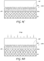
- the nano-scale patterns of the polymer layer can be uniform in size and shape.
- the sealing layer can be optically transparent. In some embodiments, there can be some space in between the sealing layer and the functionalizable layer to allow sample fluid flowing through.
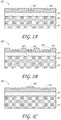
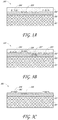
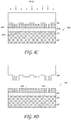
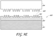
- the embossed stamp 804 is contacted with an upper surface of the photocurable polymer layer 803a, then pressure is applied to the embossed stamp 804 or the substrate 800 as shown in FIG. 8B .
- the nano-scale patterns 805 and 806 are formed in the photocurable polymer layer 803a of the substrate 800.
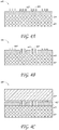
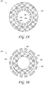
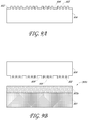
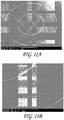
- FIG. 12A depicts serpentine fluidic channels and junctions formed for applications such as fluidic mixing.
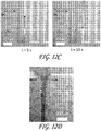
- Microfluidic filters FIG. 12B
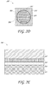
- FIG. 12D shows an optical image of the fluid flowed into a T-junction for fluid mixing.
Landscapes
- Chemical & Material Sciences (AREA)
- Health & Medical Sciences (AREA)
- Chemical Kinetics & Catalysis (AREA)
- Physics & Mathematics (AREA)
- General Physics & Mathematics (AREA)
- Medicinal Chemistry (AREA)
- Polymers & Plastics (AREA)
- Organic Chemistry (AREA)
- Analytical Chemistry (AREA)
- General Health & Medical Sciences (AREA)
- Hematology (AREA)
- Clinical Laboratory Science (AREA)
- Laminated Bodies (AREA)
- Exposure Of Semiconductors, Excluding Electron Or Ion Beam Exposure (AREA)
- Apparatus Associated With Microorganisms And Enzymes (AREA)
- Shaping Of Tube Ends By Bending Or Straightening (AREA)
- Polymerisation Methods In General (AREA)
- Inorganic Compounds Of Heavy Metals (AREA)
- Oxygen, Ozone, And Oxides In General (AREA)
Priority Applications (1)
| Application Number | Priority Date | Filing Date | Title |
|---|---|---|---|
| EP19183860.6A EP3572875A1 (en) | 2013-12-19 | 2014-12-17 | Roll-to-roll process of preparing a patterned substrate and patterned substrate prepared by the same process |
Applications Claiming Priority (2)
| Application Number | Priority Date | Filing Date | Title |
|---|---|---|---|
| US201361918582P | 2013-12-19 | 2013-12-19 | |
| PCT/US2014/070777 WO2015095291A1 (en) | 2013-12-19 | 2014-12-17 | Substrates comprising nano-patterning surfaces and methods of preparing thereof |
Related Child Applications (1)
| Application Number | Title | Priority Date | Filing Date |
|---|---|---|---|
| EP19183860.6A Division EP3572875A1 (en) | 2013-12-19 | 2014-12-17 | Roll-to-roll process of preparing a patterned substrate and patterned substrate prepared by the same process |
Publications (2)
| Publication Number | Publication Date |
|---|---|
| EP3084523A1 EP3084523A1 (en) | 2016-10-26 |
| EP3084523B1 true EP3084523B1 (en) | 2019-07-03 |
Family
ID=52293256
Family Applications (2)
| Application Number | Title | Priority Date | Filing Date |
|---|---|---|---|
| EP14824694.5A Active EP3084523B1 (en) | 2013-12-19 | 2014-12-17 | Substrates comprising nano-patterning surfaces and methods of preparing thereof |
| EP19183860.6A Pending EP3572875A1 (en) | 2013-12-19 | 2014-12-17 | Roll-to-roll process of preparing a patterned substrate and patterned substrate prepared by the same process |
Family Applications After (1)
| Application Number | Title | Priority Date | Filing Date |
|---|---|---|---|
| EP19183860.6A Pending EP3572875A1 (en) | 2013-12-19 | 2014-12-17 | Roll-to-roll process of preparing a patterned substrate and patterned substrate prepared by the same process |
Country Status (7)
| Country | Link |
|---|---|
| US (4) | US10682829B2 (enExample) |
| EP (2) | EP3084523B1 (enExample) |
| JP (3) | JP6683608B2 (enExample) |
| CN (2) | CN105874385B (enExample) |
| AU (1) | AU2014364898B2 (enExample) |
| CA (2) | CA2928598C (enExample) |
| WO (1) | WO2015095291A1 (enExample) |
Families Citing this family (37)
| Publication number | Priority date | Publication date | Assignee | Title |
|---|---|---|---|---|
| EP3084523B1 (en) * | 2013-12-19 | 2019-07-03 | Illumina, Inc. | Substrates comprising nano-patterning surfaces and methods of preparing thereof |
| DK3218511T3 (da) * | 2014-11-11 | 2020-07-20 | Illumina Cambridge Ltd | Fremgangsmåder og arrays til frembringelse og sekventering af monoklonale klynger af nukleinsyre |
| WO2017007753A1 (en) * | 2015-07-07 | 2017-01-12 | Illumina, Inc. | Selective surface patterning via nanoimrinting |
| US20180207920A1 (en) * | 2015-07-17 | 2018-07-26 | Illumina, Inc. | Polymer sheets for sequencing applications |
| JP6975466B2 (ja) * | 2016-02-02 | 2021-12-01 | 学校法人沖縄科学技術大学院大学学園 | アミノシランを用いるマイクロ及びナノコンタクトプリンティング:多重バイオアッセイのためのマイクロ流体デバイスのパターニング表面 |
| SG11201809376WA (en) | 2016-05-18 | 2018-12-28 | Illumina Inc | Self assembled patterning using patterned hydrophobic surfaces |
| DE102016109693B4 (de) * | 2016-05-25 | 2022-10-27 | Infineon Technologies Ag | Verfahren zum Trennen von Halbleiterdies von einem Halbleitersubstrat und Halbleitersubstratanordnung |
| JP7053587B2 (ja) | 2016-09-27 | 2022-04-12 | イラミーナ インコーポレーテッド | インプリント基板 |
| CN106501520A (zh) * | 2016-10-18 | 2017-03-15 | 成都市亿泰科技有限公司 | 一种基于微流体毛细结构的毒品检测试纸及其制备方法 |
| IL267444B2 (en) | 2016-12-22 | 2024-12-01 | Illumina Inc | Arrays including a resin film and a patterned polymer layer |
| MX2019006753A (es) * | 2016-12-22 | 2020-01-30 | Illumina Inc | Paquete de celda de flujo y metodo para fabricar el mismo. |
| MY203439A (en) * | 2016-12-22 | 2024-06-28 | Illumina Inc | Array including sequencing primer and non-sequencing entity |
| IL267443B2 (en) * | 2016-12-22 | 2023-10-01 | Illumina Inc | Imprinting apparatus |
| US11261085B2 (en) | 2017-05-03 | 2022-03-01 | Nanotech Security Corp. | Methods for micro and nano fabrication by selective template removal |
| WO2018201248A1 (en) * | 2017-05-03 | 2018-11-08 | Nanotech Security Corp. | Methods for micro and nano fabrication by selective template removal |
| US10503456B2 (en) | 2017-05-05 | 2019-12-10 | Nvidia Corporation | Method and apparatus for rendering perspective-correct images for a tilted multi-display environment |
| WO2018225707A1 (ja) * | 2017-06-09 | 2018-12-13 | 三井化学株式会社 | 微細凹凸パターン付き基板の製造方法、樹脂組成物および積層体 |
| DE102017217179A1 (de) * | 2017-09-27 | 2019-03-28 | Disco Corporation | Mikrofluidisches System oder mikrofluidische Einrichtung und Verfahren zum Herstellen eines mikrofluidischen Systems oder einer mikrofluidischen Einrichtung |
| KR102091622B1 (ko) * | 2017-10-10 | 2020-03-20 | 삼육대학교산학협력단 | 양자점-중합체 합성물의 패턴화 방법 및 패턴화된 양자점-중합체 합성물을 포함하는 기판 |
| US10344328B2 (en) | 2017-11-17 | 2019-07-09 | Ultima Genomics, Inc. | Methods for biological sample processing and analysis |
| US11499962B2 (en) | 2017-11-17 | 2022-11-15 | Ultima Genomics, Inc. | Methods and systems for analyte detection and analysis |
| CA3066535C (en) | 2017-12-21 | 2022-08-02 | Illumina, Inc. | Flow cells with hydrogel coating |
| RU2741805C1 (ru) | 2017-12-22 | 2021-01-28 | Иллюмина, Инк. | Каталитически активные вещества |
| US12239980B2 (en) | 2018-12-07 | 2025-03-04 | Ultima Genomics, Inc. | Implementing barriers for controlled environments during sample processing and detection |
| US10512911B1 (en) | 2018-12-07 | 2019-12-24 | Ultima Genomics, Inc. | Implementing barriers for controlled environments during sample processing and detection |
| CN119960261A (zh) * | 2018-12-31 | 2025-05-09 | Asml荷兰有限公司 | 用于预测抗蚀剂变形的方法 |
| US11118223B2 (en) | 2019-03-14 | 2021-09-14 | Ultima Genomics, Inc. | Methods, devices, and systems for analyte detection and analysis |
| US10852518B1 (en) | 2019-03-14 | 2020-12-01 | Ultima Genomics, Inc. | Methods, devices, and systems for analyte detection and analysis |
| US10830703B1 (en) | 2019-03-14 | 2020-11-10 | Ultima Genomics, Inc. | Methods, devices, and systems for analyte detection and analysis |
| US10900078B2 (en) | 2019-03-14 | 2021-01-26 | Ultima Genomics, Inc. | Methods, devices, and systems for analyte detection and analysis |
| NL2023679B1 (en) * | 2019-08-09 | 2021-04-13 | Illumina Inc | System and method for patterning flow cell substrates |
| CN110596950A (zh) * | 2019-10-29 | 2019-12-20 | 京东方科技集团股份有限公司 | 一种量子点彩色滤光层及其制作方法、显示面板及装置 |
| EP3839625A1 (fr) * | 2019-12-18 | 2021-06-23 | Nivarox-FAR S.A. | Procede de fabrication d'un composant horloger et composant obtenu selon ce procede |
| US20240011975A1 (en) * | 2020-09-15 | 2024-01-11 | 3M Innovative Properties Company | Nanopatterned Films with Patterned Surface Chemistry |
| CN116762007A (zh) | 2020-12-31 | 2023-09-15 | 3M创新有限公司 | 具有图案化表面化学成分的纳米图案化膜 |
| WO2024025806A1 (en) * | 2022-07-27 | 2024-02-01 | Illumina, Inc. | Motion feedback using patterned flowcells |
| CN119161945A (zh) * | 2023-06-20 | 2024-12-20 | 深圳市真迈生物科技有限公司 | 芯片及其制备方法 |
Family Cites Families (126)
| Publication number | Priority date | Publication date | Assignee | Title |
|---|---|---|---|---|
| GB8822228D0 (en) | 1988-09-21 | 1988-10-26 | Southern E M | Support-bound oligonucleotides |
| US5077210A (en) * | 1989-01-13 | 1991-12-31 | Eigler Frances S | Immobilization of active agents on substrates with a silane and heterobifunctional crosslinking agent |
| US6346413B1 (en) | 1989-06-07 | 2002-02-12 | Affymetrix, Inc. | Polymer arrays |
| US5800992A (en) | 1989-06-07 | 1998-09-01 | Fodor; Stephen P.A. | Method of detecting nucleic acids |
| DE3924454A1 (de) | 1989-07-24 | 1991-02-07 | Cornelis P Prof Dr Hollenberg | Die anwendung von dna und dna-technologie fuer die konstruktion von netzwerken zur verwendung in der chip-konstruktion und chip-produktion (dna chips) |
| US5770358A (en) | 1991-09-18 | 1998-06-23 | Affymax Technologies N.V. | Tagged synthetic oligomer libraries |
| US6017696A (en) | 1993-11-01 | 2000-01-25 | Nanogen, Inc. | Methods for electronic stringency control for molecular biological analysis and diagnostics |
| DE69233087T2 (de) | 1991-11-22 | 2003-12-24 | Affymetrix, Inc. (N.D.Ges.D.Staates Delaware) | Verfahren zur Herstellung von Polymerarrays |
| EP0675966B1 (en) | 1992-02-19 | 2004-10-06 | The Public Health Research Institute Of The City Of New York, Inc. | Novel oligonucleotide arrays and their use for sorting, isolating, sequencing, and manipulating nucleic acids |
| US5583211A (en) | 1992-10-29 | 1996-12-10 | Beckman Instruments, Inc. | Surface activated organic polymers useful for location - specific attachment of nucleic acids, peptides, proteins and oligosaccharides |
| WO1995011995A1 (en) | 1993-10-26 | 1995-05-04 | Affymax Technologies N.V. | Arrays of nucleic acid probes on biological chips |
| US5472672A (en) | 1993-10-22 | 1995-12-05 | The Board Of Trustees Of The Leland Stanford Junior University | Apparatus and method for polymer synthesis using arrays |
| US6156501A (en) | 1993-10-26 | 2000-12-05 | Affymetrix, Inc. | Arrays of modified nucleic acid probes and methods of use |
| US5429807A (en) | 1993-10-28 | 1995-07-04 | Beckman Instruments, Inc. | Method and apparatus for creating biopolymer arrays on a solid support surface |
| US7172864B1 (en) * | 1993-11-01 | 2007-02-06 | Nanogen | Methods for electronically-controlled enzymatic reactions |
| US5807522A (en) | 1994-06-17 | 1998-09-15 | The Board Of Trustees Of The Leland Stanford Junior University | Methods for fabricating microarrays of biological samples |
| US5641658A (en) | 1994-08-03 | 1997-06-24 | Mosaic Technologies, Inc. | Method for performing amplification of nucleic acid with two primers bound to a single solid support |
| US5556752A (en) | 1994-10-24 | 1996-09-17 | Affymetrix, Inc. | Surface-bound, unimolecular, double-stranded DNA |
| US5624711A (en) | 1995-04-27 | 1997-04-29 | Affymax Technologies, N.V. | Derivatization of solid supports and methods for oligomer synthesis |
| US5545531A (en) | 1995-06-07 | 1996-08-13 | Affymax Technologies N.V. | Methods for making a device for concurrently processing multiple biological chip assays |
| AU7398996A (en) | 1995-10-11 | 1997-04-30 | Luminex Corporation | Multiplexed analysis of clinical specimens apparatus and method |
| US5658734A (en) | 1995-10-17 | 1997-08-19 | International Business Machines Corporation | Process for synthesizing chemical compounds |
| US6458530B1 (en) | 1996-04-04 | 2002-10-01 | Affymetrix Inc. | Selecting tag nucleic acids |
| SE9602545L (sv) * | 1996-06-25 | 1997-12-26 | Michael Mecklenburg | Metod för att diskriminera komplexa biologiska prover |
| US6297006B1 (en) | 1997-01-16 | 2001-10-02 | Hyseq, Inc. | Methods for sequencing repetitive sequences and for determining the order of sequence subfragments |
| EP1498494A3 (en) | 1997-04-01 | 2007-06-20 | Solexa Ltd. | Method of nucleic acid sequencing |
| US6465178B2 (en) | 1997-09-30 | 2002-10-15 | Surmodics, Inc. | Target molecule attachment to surfaces |
| US6485944B1 (en) | 1997-10-10 | 2002-11-26 | President And Fellows Of Harvard College | Replica amplification of nucleic acid arrays |
| US6087102A (en) | 1998-01-07 | 2000-07-11 | Clontech Laboratories, Inc. | Polymeric arrays and methods for their use in binding assays |
| US6287776B1 (en) | 1998-02-02 | 2001-09-11 | Signature Bioscience, Inc. | Method for detecting and classifying nucleic acid hybridization |
| JP3944996B2 (ja) | 1998-03-05 | 2007-07-18 | 株式会社日立製作所 | Dnaプローブアレー |
| US6031078A (en) | 1998-06-16 | 2000-02-29 | Millennium Pharmaceuticals, Inc. | MTbx protein and nucleic acid molecules and uses therefor |
| US6682942B1 (en) * | 1998-07-14 | 2004-01-27 | Zyomyx, Inc. | Microdevices for screening biomolecules |
| AR021833A1 (es) | 1998-09-30 | 2002-08-07 | Applied Research Systems | Metodos de amplificacion y secuenciacion de acido nucleico |
| US6277628B1 (en) | 1998-10-02 | 2001-08-21 | Incyte Genomics, Inc. | Linear microarrays |
| US6391937B1 (en) | 1998-11-25 | 2002-05-21 | Motorola, Inc. | Polyacrylamide hydrogels and hydrogel arrays made from polyacrylamide reactive prepolymers |
| DK1923471T3 (da) | 1999-04-20 | 2013-04-02 | Illumina Inc | Detektion af nukleinsyrereaktioner på bead-arrays |
| US6355431B1 (en) | 1999-04-20 | 2002-03-12 | Illumina, Inc. | Detection of nucleic acid amplification reactions using bead arrays |
| US6921638B2 (en) * | 1999-06-25 | 2005-07-26 | Amersham Biosciences Ab | Hydrogel-based microarray signal amplification methods and devices therefor |
| US6664061B2 (en) | 1999-06-25 | 2003-12-16 | Amersham Biosciences Ab | Use and evaluation of a [2+2] photoaddition in immobilization of oligonucleotides on a three-dimensional hydrogel matrix |
| US6372813B1 (en) | 1999-06-25 | 2002-04-16 | Motorola | Methods and compositions for attachment of biomolecules to solid supports, hydrogels, and hydrogel arrays |
| US7501245B2 (en) * | 1999-06-28 | 2009-03-10 | Helicos Biosciences Corp. | Methods and apparatuses for analyzing polynucleotide sequences |
| US6770441B2 (en) | 2000-02-10 | 2004-08-03 | Illumina, Inc. | Array compositions and methods of making same |
| AU2001241723A1 (en) | 2000-02-25 | 2001-09-03 | Affymetrix, Inc. | Methods for multi-stage solid phase amplification of nucleic acids |
| BR0015893A (pt) * | 2000-06-09 | 2003-07-01 | 3M Innovative Properties Co | Montagem de laminado que retem imagem, e, métodos de formar um laminado e um meio que retenha imagem |
| AU2001279244A1 (en) | 2000-08-09 | 2002-02-18 | Motorola, Inc. | The use and evaluation of a (2+2) photocycloaddition in immobilization of oligonucleotides on a three-dimensional hydrogel matrix |
| EP1330306A2 (en) * | 2000-10-10 | 2003-07-30 | BioTrove, Inc. | Apparatus for assay, synthesis and storage, and methods of manufacture, use, and manipulation thereof |
| AR031640A1 (es) | 2000-12-08 | 2003-09-24 | Applied Research Systems | Amplificacion isotermica de acidos nucleicos en un soporte solido |
| JP2002184719A (ja) | 2000-12-19 | 2002-06-28 | Matsushita Electric Ind Co Ltd | パターン形成方法 |
| US20060207877A1 (en) * | 2001-01-30 | 2006-09-21 | Walter Schmidt | Microfluidic device with various surface properties fabricated in multilayer body by plasma etching |
| DE10117663B4 (de) * | 2001-04-09 | 2004-09-02 | Samsung SDI Co., Ltd., Suwon | Verfahren zur Herstellung von Matrixanordnungen auf Basis verschiedenartiger organischer leitfähiger Materialien |
| EP1267169B1 (en) * | 2001-05-21 | 2004-12-15 | Fuji Photo Film Co., Ltd. | Biochemical analysis unit and method for its production |
| DE10392199T5 (de) * | 2002-01-18 | 2005-01-05 | Avery Dennison Corp., Pasadena | Folie mit Mikroarchitektur |
| US7514045B2 (en) * | 2002-01-18 | 2009-04-07 | Avery Dennison Corporation | Covered microchamber structures |
| US20040002090A1 (en) | 2002-03-05 | 2004-01-01 | Pascal Mayer | Methods for detecting genome-wide sequence variations associated with a phenotype |
| US20040258885A1 (en) * | 2002-09-05 | 2004-12-23 | Kreutter Nathan P. | Etched dielectric film in microfluidic devices |
| WO2004086471A1 (en) | 2003-03-27 | 2004-10-07 | Korea Institute Of Machinery & Materials | Uv nanoimprint lithography process using elementwise embossed stamp and selectively additive pressurization |
| JP4007269B2 (ja) | 2003-07-29 | 2007-11-14 | オムロン株式会社 | 生体分子の形状転写方法、チップ基板の製造方法及びバイオチップの製造方法 |
| EP1694731B1 (en) | 2003-09-23 | 2012-03-28 | University Of North Carolina At Chapel Hill | Photocurable perfluoropolyethers for use as novel materials in microfluidic devices |
| US20050121782A1 (en) | 2003-12-05 | 2005-06-09 | Koichiro Nakamura | Selectively adherent substrate and method for producing the same |
| JP2005208044A (ja) | 2003-12-25 | 2005-08-04 | Nippon Sheet Glass Co Ltd | 生体関連物質選択付着性基板 |
| WO2005065814A1 (en) | 2004-01-07 | 2005-07-21 | Solexa Limited | Modified molecular arrays |
| US7597814B2 (en) | 2004-03-23 | 2009-10-06 | Hewlett Packard Development Company, L.P. | Structure formed with template having nanoscale features |
| US20060021533A1 (en) * | 2004-07-30 | 2006-02-02 | Jeans Albert H | Imprint stamp |
| US7459197B2 (en) * | 2004-11-30 | 2008-12-02 | Lucent Technologies Inc. | Reversibly adaptive rough micro- and nano-structures |
| US20090011946A1 (en) * | 2004-12-20 | 2009-01-08 | Kalinex | Use of Sequence Specific Polymers in Chemical Detection |
| EP1700680A1 (en) | 2005-03-09 | 2006-09-13 | EPFL Ecole Polytechnique Fédérale de Lausanne | Easy release fluoropolymer molds for micro- and nano-pattern replication |
| JP4534817B2 (ja) | 2005-03-16 | 2010-09-01 | 住友ベークライト株式会社 | 蛋白質の検出方法及びペプチドの検出方法 |
| US20090042736A1 (en) * | 2005-04-18 | 2009-02-12 | Johan Gerrit Bomer | Biochip and process for the production of a biochip |
| US7331655B2 (en) * | 2005-05-19 | 2008-02-19 | Xerox Corporation | Fluid coupler and a device arranged with the same |
| CN102016814B (zh) * | 2005-06-17 | 2013-10-23 | 北卡罗来纳大学查珀尔希尔分校 | 纳米粒子制备方法、系统及材料 |
| CN101283042A (zh) * | 2005-08-09 | 2008-10-08 | 查珀尔希尔北卡罗来纳大学 | 制造微流体器件的方法和材料 |
| US7482280B2 (en) | 2005-08-15 | 2009-01-27 | Taiwan Semiconductor Manufacturing Company, Ltd. | Method for forming a lithography pattern |
| US8011916B2 (en) | 2005-09-06 | 2011-09-06 | Canon Kabushiki Kaisha | Mold, imprint apparatus, and process for producing structure |
| US8084116B2 (en) * | 2005-09-30 | 2011-12-27 | Alcatel Lucent | Surfaces physically transformable by environmental changes |
| GB0522310D0 (en) | 2005-11-01 | 2005-12-07 | Solexa Ltd | Methods of preparing libraries of template polynucleotides |
| WO2007056338A2 (en) * | 2005-11-08 | 2007-05-18 | Surmodics, Inc. | Ultra-thin photo-polymeric coatings and uses thereof |
| CA2631248C (en) * | 2005-11-28 | 2016-01-12 | Pacific Biosciences Of California, Inc. | Uniform surfaces for hybrid material substrates and methods for making and using same |
| US8944804B2 (en) * | 2006-01-04 | 2015-02-03 | Liquidia Technologies, Inc. | Nanostructured surfaces for biomedical/biomaterial applications and processes thereof |
| DE102006029032A1 (de) * | 2006-02-17 | 2007-08-23 | Poly-An Gesellschaft zur Herstellung von Polymeren für spezielle Anwendungen und Analytik mbH | Vorrichtung, Verfahren und Kit zum Nachweis von Analyten in einer Probe |
| EP2021503A1 (en) | 2006-03-17 | 2009-02-11 | Solexa Ltd. | Isothermal methods for creating clonal single molecule arrays |
| CA2648149A1 (en) | 2006-03-31 | 2007-11-01 | Solexa, Inc. | Systems and devices for sequence by synthesis analysis |
| US8764996B2 (en) * | 2006-10-18 | 2014-07-01 | 3M Innovative Properties Company | Methods of patterning a material on polymeric substrates |
| US8128393B2 (en) | 2006-12-04 | 2012-03-06 | Liquidia Technologies, Inc. | Methods and materials for fabricating laminate nanomolds and nanoparticles therefrom |
| US20100190654A1 (en) * | 2006-12-05 | 2010-07-29 | Liquidia Technologies , Inc. | Nanoarrays and methods and materials for fabricating same |
| US20080233280A1 (en) | 2007-03-22 | 2008-09-25 | Graciela Beatriz Blanchet | Method to form a pattern of functional material on a substrate by treating a surface of a stamp |
| US8597630B2 (en) * | 2007-04-19 | 2013-12-03 | University Of Massachusetts | Thermal-responsive polymer networks, compositions, and methods and applications related thereto |
| US20100111770A1 (en) * | 2007-06-07 | 2010-05-06 | Samsung Electronics Co., Ltd. | Microfluidic Chip and Method of Fabricating The Same |
| US20100098761A1 (en) * | 2007-08-03 | 2010-04-22 | University Of Massachusetts Medical School | Polymer Compositions For Biomedical And Material Applications |
| WO2009033056A1 (en) * | 2007-09-06 | 2009-03-12 | Bioscale, Inc. | Reusable detection surfaces and methods of using same |
| US20090243584A1 (en) * | 2008-03-25 | 2009-10-01 | Guigen Zhang | Fabrication of microstructures integrated with nanopillars along with their applications as electrodes in sensors |
| US8334217B2 (en) * | 2008-06-09 | 2012-12-18 | Rolith Inc. | Material deposition over template |
| TWI376568B (en) * | 2008-06-12 | 2012-11-11 | Univ Nat Cheng Kung | Method for manufacturing roller mold |
| US20100053623A1 (en) * | 2008-08-27 | 2010-03-04 | Sunghoon Kwon | Membrane and fabrication method thereof |
| EP2559533B1 (en) * | 2008-09-26 | 2020-04-15 | United Technologies Corporation | Casting |
| EP2391725A4 (en) * | 2009-01-30 | 2013-01-02 | Us Health | METHOD AND SYSTEMS FOR CLEANING TRANSMITTING AND / OR MANIPULATING NUCLEIC ACIDS |
| US20120010636A1 (en) * | 2009-02-11 | 2012-01-12 | Nanyang Technological University | Multi-layered surgical prosthesis |
| FR2943344B1 (fr) * | 2009-03-18 | 2011-04-15 | Commissariat Energie Atomique | Nouveaux composes silanes porteurs d'une chaine carbonee cyclique comprenant une fonction alcyne pour fonctionnaliser des supports solides et immobiliser sur ces supports des molecules biologiques |
| US8163834B2 (en) * | 2009-03-18 | 2012-04-24 | Dublin City University | Photoresponsive ionogel |
| JP5518538B2 (ja) | 2009-03-26 | 2014-06-11 | 富士フイルム株式会社 | レジスト組成物、レジスト層、インプリント方法、パターン形成体、磁気記録媒体の製造方法、及び磁気記録媒体 |
| WO2010117102A1 (ko) * | 2009-04-09 | 2010-10-14 | 서강대학교 산학협력단 | 콜로이드 입자들을 단결정들로 정렬하는 방법 |
| EP2284252A1 (en) * | 2009-08-13 | 2011-02-16 | Sony DADC Austria AG | Surface-structured device for life-science applications |
| US9465296B2 (en) | 2010-01-12 | 2016-10-11 | Rolith, Inc. | Nanopatterning method and apparatus |
| BR112012024411A2 (pt) * | 2010-03-31 | 2016-05-31 | Kaneka Corp | estrutura, chip para sensor de ressonância de plásmon de superfície localizada, sensor de ressonância de plásmon de superfície localizada e métodos de fabricação |
| BR112012029516B1 (pt) * | 2010-05-05 | 2020-04-28 | Ethicon Endo Surgery Llc | dispositivo de retenção de tecido |
| JP5464058B2 (ja) | 2010-06-02 | 2014-04-09 | 大日本印刷株式会社 | ナノインプリントモールドの製造方法、光学素子の製造方法、およびレジストパターンの形成方法 |
| JP5616309B2 (ja) * | 2010-12-01 | 2014-10-29 | アークレイ株式会社 | デバイス及びその製造方法 |
| WO2012077324A1 (ja) | 2010-12-07 | 2012-06-14 | パナソニック株式会社 | バイオチップおよびこれを用いたアレイ基板 |
| CN102169086B (zh) * | 2010-12-31 | 2013-01-09 | 清华大学 | 用于单分子检测的分子载体 |
| US8951781B2 (en) | 2011-01-10 | 2015-02-10 | Illumina, Inc. | Systems, methods, and apparatuses to image a sample for biological or chemical analysis |
| CN103459583B (zh) * | 2011-03-08 | 2015-11-25 | 公立大学法人大阪府立大学 | 传感器、传感器的制造方法及聚合物层 |
| US8778848B2 (en) * | 2011-06-09 | 2014-07-15 | Illumina, Inc. | Patterned flow-cells useful for nucleic acid analysis |
| PL2734574T3 (pl) * | 2011-07-18 | 2020-05-18 | Celgard Llc | Materiały polimerowe modyfikowane powierzchniowo, modyfikowane funkcjonalizowane polimery, polimery funkcjonalne i sposoby |
| KR101344340B1 (ko) * | 2011-08-12 | 2013-12-24 | 포항공과대학교 산학협력단 | 멤브레인과 그 제조 방법 |
| EP3305400A3 (en) * | 2011-10-28 | 2018-06-06 | Illumina, Inc. | Microarray fabrication system and method |
| CA2758622A1 (en) * | 2011-11-17 | 2013-05-17 | Allan R. MANNINEN | Coextruded laser weld enabled polymer film or filament and fabrics made therefrom |
| US9266260B2 (en) * | 2011-12-20 | 2016-02-23 | Massachusetts Institute Of Technology | Precision continuous stamp casting method for roll-based soft lithography |
| DE102012103174B3 (de) * | 2012-04-12 | 2013-09-19 | Technische Universität Ilmenau | Verfahren zur Herstellung eines mikrostrukturierten Formkörpers |
| US9012022B2 (en) * | 2012-06-08 | 2015-04-21 | Illumina, Inc. | Polymer coatings |
| US8895249B2 (en) * | 2012-06-15 | 2014-11-25 | Illumina, Inc. | Kinetic exclusion amplification of nucleic acid libraries |
| JP6386700B2 (ja) * | 2012-07-04 | 2018-09-05 | キヤノン株式会社 | 構造体、光学部材、反射防止膜、撥水性膜、質量分析用基板、位相板、構造体の製造方法、及び反射防止膜の製造方法 |
| US9512422B2 (en) * | 2013-02-26 | 2016-12-06 | Illumina, Inc. | Gel patterned surfaces |
| MX363806B (es) | 2013-07-01 | 2019-04-03 | Illumina Inc | Funcionalización de superficies sin catalizador e injerto de polímeros.. |
| US10006085B2 (en) * | 2013-11-04 | 2018-06-26 | The Regents Of The University Of California | Nanostructured arrays on flexible polymer films |
| EP3084523B1 (en) * | 2013-12-19 | 2019-07-03 | Illumina, Inc. | Substrates comprising nano-patterning surfaces and methods of preparing thereof |
| CN107090023B (zh) | 2017-03-23 | 2020-06-05 | 桂林八加一药业股份有限公司 | 一种选择性tnfr1拮抗肽sn10及其在类风湿性关节炎中的应用 |
-
2014
- 2014-12-17 EP EP14824694.5A patent/EP3084523B1/en active Active
- 2014-12-17 CA CA2928598A patent/CA2928598C/en active Active
- 2014-12-17 AU AU2014364898A patent/AU2014364898B2/en active Active
- 2014-12-17 CN CN201480064276.4A patent/CN105874385B/zh active Active
- 2014-12-17 EP EP19183860.6A patent/EP3572875A1/en active Pending
- 2014-12-17 US US15/025,866 patent/US10682829B2/en active Active
- 2014-12-17 WO PCT/US2014/070777 patent/WO2015095291A1/en not_active Ceased
- 2014-12-17 CA CA3171807A patent/CA3171807A1/en active Pending
- 2014-12-17 JP JP2016532111A patent/JP6683608B2/ja active Active
- 2014-12-17 CN CN202110878609.9A patent/CN114089597B/zh active Active
-
2020
- 2020-03-26 JP JP2020055517A patent/JP7096853B2/ja active Active
- 2020-05-21 US US16/880,809 patent/US11110683B2/en not_active Expired - Fee Related
-
2021
- 2021-08-23 US US17/409,649 patent/US12151460B2/en active Active
-
2022
- 2022-06-24 JP JP2022101879A patent/JP7407240B2/ja active Active
-
2024
- 2024-11-08 US US18/942,108 patent/US20250091313A1/en active Pending
Also Published As
| Publication number | Publication date |
|---|---|
| CA2928598A1 (en) | 2015-06-25 |
| CA3171807A1 (en) | 2015-06-25 |
| CA2928598C (en) | 2022-11-29 |
| JP7096853B2 (ja) | 2022-07-06 |
| EP3572875A1 (en) | 2019-11-27 |
| JP7407240B2 (ja) | 2023-12-28 |
| JP2020129660A (ja) | 2020-08-27 |
| JP2017504183A (ja) | 2017-02-02 |
| CN114089597B (zh) | 2025-03-14 |
| US12151460B2 (en) | 2024-11-26 |
| US20250091313A1 (en) | 2025-03-20 |
| US10682829B2 (en) | 2020-06-16 |
| US20210379858A1 (en) | 2021-12-09 |
| EP3084523A1 (en) | 2016-10-26 |
| CN105874385B (zh) | 2021-08-20 |
| US11110683B2 (en) | 2021-09-07 |
| AU2014364898A1 (en) | 2016-05-12 |
| CN114089597A (zh) | 2022-02-25 |
| AU2014364898B2 (en) | 2018-07-26 |
| US20200282693A1 (en) | 2020-09-10 |
| JP6683608B2 (ja) | 2020-04-22 |
| US20160246170A1 (en) | 2016-08-25 |
| JP2022125109A (ja) | 2022-08-26 |
| WO2015095291A1 (en) | 2015-06-25 |
| CN105874385A (zh) | 2016-08-17 |
Similar Documents
| Publication | Publication Date | Title |
|---|---|---|
| US12151460B2 (en) | Substrates comprising nano-patterning surfaces and methods of preparing thereof | |
| EP3325648B1 (en) | Polymer sheets for sequencing applications | |
| IL262516A (en) | Self-assembly pattern using sampled hydrophobic surfaces | |
| AU2017382202A1 (en) | Arrays including a resin film and a patterned polymer layer | |
| HK40017406A (en) | Roll-to-roll process of preparing a patterned substrate and patterned substrate prepared by the same process | |
| JP2026502023A (ja) | パターニングされた基材を有するフローセル | |
| US20230330659A1 (en) | Substrate with orthogonally functional nanodomains | |
| EP4355476A1 (en) | Hydrogel-free surface functionalization for sequencing | |
| EP4633793A2 (en) | Flow cells | |
| HK40003935A (en) | Self assembled patterning using patterned hydrophobic surfaces |
Legal Events
| Date | Code | Title | Description |
|---|---|---|---|
| PUAI | Public reference made under article 153(3) epc to a published international application that has entered the european phase |
Free format text: ORIGINAL CODE: 0009012 |
|
| 17P | Request for examination filed |
Effective date: 20160708 |
|
| AK | Designated contracting states |
Kind code of ref document: A1 Designated state(s): AL AT BE BG CH CY CZ DE DK EE ES FI FR GB GR HR HU IE IS IT LI LT LU LV MC MK MT NL NO PL PT RO RS SE SI SK SM TR |
|
| AX | Request for extension of the european patent |
Extension state: BA ME |
|
| DAX | Request for extension of the european patent (deleted) | ||
| GRAP | Despatch of communication of intention to grant a patent |
Free format text: ORIGINAL CODE: EPIDOSNIGR1 |
|
| STAA | Information on the status of an ep patent application or granted ep patent |
Free format text: STATUS: GRANT OF PATENT IS INTENDED |
|
| RAP1 | Party data changed (applicant data changed or rights of an application transferred) |
Owner name: ILLUMINA, INC. |
|
| INTG | Intention to grant announced |
Effective date: 20190123 |
|
| GRAS | Grant fee paid |
Free format text: ORIGINAL CODE: EPIDOSNIGR3 |
|
| GRAA | (expected) grant |
Free format text: ORIGINAL CODE: 0009210 |
|
| STAA | Information on the status of an ep patent application or granted ep patent |
Free format text: STATUS: THE PATENT HAS BEEN GRANTED |
|
| AK | Designated contracting states |
Kind code of ref document: B1 Designated state(s): AL AT BE BG CH CY CZ DE DK EE ES FI FR GB GR HR HU IE IS IT LI LT LU LV MC MK MT NL NO PL PT RO RS SE SI SK SM TR |
|
| REG | Reference to a national code |
Ref country code: GB Ref legal event code: FG4D |
|
| REG | Reference to a national code |
Ref country code: CH Ref legal event code: EP Ref country code: AT Ref legal event code: REF Ref document number: 1151709 Country of ref document: AT Kind code of ref document: T Effective date: 20190715 |
|
| REG | Reference to a national code |
Ref country code: IE Ref legal event code: FG4D |
|
| REG | Reference to a national code |
Ref country code: DE Ref legal event code: R096 Ref document number: 602014049599 Country of ref document: DE |
|
| REG | Reference to a national code |
Ref country code: CH Ref legal event code: NV Representative=s name: TROESCH SCHEIDEGGER WERNER AG, CH |
|
| REG | Reference to a national code |
Ref country code: NL Ref legal event code: FP |
|
| REG | Reference to a national code |
Ref country code: SE Ref legal event code: TRGR |
|
| REG | Reference to a national code |
Ref country code: LT Ref legal event code: MG4D |
|
| REG | Reference to a national code |
Ref country code: AT Ref legal event code: MK05 Ref document number: 1151709 Country of ref document: AT Kind code of ref document: T Effective date: 20190703 |
|
| PG25 | Lapsed in a contracting state [announced via postgrant information from national office to epo] |
Ref country code: AT Free format text: LAPSE BECAUSE OF FAILURE TO SUBMIT A TRANSLATION OF THE DESCRIPTION OR TO PAY THE FEE WITHIN THE PRESCRIBED TIME-LIMIT Effective date: 20190703 Ref country code: NO Free format text: LAPSE BECAUSE OF FAILURE TO SUBMIT A TRANSLATION OF THE DESCRIPTION OR TO PAY THE FEE WITHIN THE PRESCRIBED TIME-LIMIT Effective date: 20191003 Ref country code: BG Free format text: LAPSE BECAUSE OF FAILURE TO SUBMIT A TRANSLATION OF THE DESCRIPTION OR TO PAY THE FEE WITHIN THE PRESCRIBED TIME-LIMIT Effective date: 20191003 Ref country code: HR Free format text: LAPSE BECAUSE OF FAILURE TO SUBMIT A TRANSLATION OF THE DESCRIPTION OR TO PAY THE FEE WITHIN THE PRESCRIBED TIME-LIMIT Effective date: 20190703 Ref country code: FI Free format text: LAPSE BECAUSE OF FAILURE TO SUBMIT A TRANSLATION OF THE DESCRIPTION OR TO PAY THE FEE WITHIN THE PRESCRIBED TIME-LIMIT Effective date: 20190703 Ref country code: CZ Free format text: LAPSE BECAUSE OF FAILURE TO SUBMIT A TRANSLATION OF THE DESCRIPTION OR TO PAY THE FEE WITHIN THE PRESCRIBED TIME-LIMIT Effective date: 20190703 Ref country code: PT Free format text: LAPSE BECAUSE OF FAILURE TO SUBMIT A TRANSLATION OF THE DESCRIPTION OR TO PAY THE FEE WITHIN THE PRESCRIBED TIME-LIMIT Effective date: 20191104 Ref country code: LT Free format text: LAPSE BECAUSE OF FAILURE TO SUBMIT A TRANSLATION OF THE DESCRIPTION OR TO PAY THE FEE WITHIN THE PRESCRIBED TIME-LIMIT Effective date: 20190703 |
|
| PG25 | Lapsed in a contracting state [announced via postgrant information from national office to epo] |
Ref country code: IS Free format text: LAPSE BECAUSE OF FAILURE TO SUBMIT A TRANSLATION OF THE DESCRIPTION OR TO PAY THE FEE WITHIN THE PRESCRIBED TIME-LIMIT Effective date: 20191103 Ref country code: RS Free format text: LAPSE BECAUSE OF FAILURE TO SUBMIT A TRANSLATION OF THE DESCRIPTION OR TO PAY THE FEE WITHIN THE PRESCRIBED TIME-LIMIT Effective date: 20190703 Ref country code: ES Free format text: LAPSE BECAUSE OF FAILURE TO SUBMIT A TRANSLATION OF THE DESCRIPTION OR TO PAY THE FEE WITHIN THE PRESCRIBED TIME-LIMIT Effective date: 20190703 Ref country code: GR Free format text: LAPSE BECAUSE OF FAILURE TO SUBMIT A TRANSLATION OF THE DESCRIPTION OR TO PAY THE FEE WITHIN THE PRESCRIBED TIME-LIMIT Effective date: 20191004 Ref country code: AL Free format text: LAPSE BECAUSE OF FAILURE TO SUBMIT A TRANSLATION OF THE DESCRIPTION OR TO PAY THE FEE WITHIN THE PRESCRIBED TIME-LIMIT Effective date: 20190703 Ref country code: LV Free format text: LAPSE BECAUSE OF FAILURE TO SUBMIT A TRANSLATION OF THE DESCRIPTION OR TO PAY THE FEE WITHIN THE PRESCRIBED TIME-LIMIT Effective date: 20190703 |
|
| PG25 | Lapsed in a contracting state [announced via postgrant information from national office to epo] |
Ref country code: TR Free format text: LAPSE BECAUSE OF FAILURE TO SUBMIT A TRANSLATION OF THE DESCRIPTION OR TO PAY THE FEE WITHIN THE PRESCRIBED TIME-LIMIT Effective date: 20190703 |
|
| PG25 | Lapsed in a contracting state [announced via postgrant information from national office to epo] |
Ref country code: PL Free format text: LAPSE BECAUSE OF FAILURE TO SUBMIT A TRANSLATION OF THE DESCRIPTION OR TO PAY THE FEE WITHIN THE PRESCRIBED TIME-LIMIT Effective date: 20190703 Ref country code: RO Free format text: LAPSE BECAUSE OF FAILURE TO SUBMIT A TRANSLATION OF THE DESCRIPTION OR TO PAY THE FEE WITHIN THE PRESCRIBED TIME-LIMIT Effective date: 20190703 Ref country code: DK Free format text: LAPSE BECAUSE OF FAILURE TO SUBMIT A TRANSLATION OF THE DESCRIPTION OR TO PAY THE FEE WITHIN THE PRESCRIBED TIME-LIMIT Effective date: 20190703 Ref country code: IT Free format text: LAPSE BECAUSE OF FAILURE TO SUBMIT A TRANSLATION OF THE DESCRIPTION OR TO PAY THE FEE WITHIN THE PRESCRIBED TIME-LIMIT Effective date: 20190703 Ref country code: EE Free format text: LAPSE BECAUSE OF FAILURE TO SUBMIT A TRANSLATION OF THE DESCRIPTION OR TO PAY THE FEE WITHIN THE PRESCRIBED TIME-LIMIT Effective date: 20190703 |
|
| PG25 | Lapsed in a contracting state [announced via postgrant information from national office to epo] |
Ref country code: SM Free format text: LAPSE BECAUSE OF FAILURE TO SUBMIT A TRANSLATION OF THE DESCRIPTION OR TO PAY THE FEE WITHIN THE PRESCRIBED TIME-LIMIT Effective date: 20190703 Ref country code: IS Free format text: LAPSE BECAUSE OF FAILURE TO SUBMIT A TRANSLATION OF THE DESCRIPTION OR TO PAY THE FEE WITHIN THE PRESCRIBED TIME-LIMIT Effective date: 20200224 Ref country code: SK Free format text: LAPSE BECAUSE OF FAILURE TO SUBMIT A TRANSLATION OF THE DESCRIPTION OR TO PAY THE FEE WITHIN THE PRESCRIBED TIME-LIMIT Effective date: 20190703 |
|
| REG | Reference to a national code |
Ref country code: DE Ref legal event code: R097 Ref document number: 602014049599 Country of ref document: DE |
|
| PLBE | No opposition filed within time limit |
Free format text: ORIGINAL CODE: 0009261 |
|
| STAA | Information on the status of an ep patent application or granted ep patent |
Free format text: STATUS: NO OPPOSITION FILED WITHIN TIME LIMIT |
|
| PG2D | Information on lapse in contracting state deleted |
Ref country code: IS |
|
| 26N | No opposition filed |
Effective date: 20200603 |
|
| REG | Reference to a national code |
Ref country code: BE Ref legal event code: MM Effective date: 20191231 |
|
| PG25 | Lapsed in a contracting state [announced via postgrant information from national office to epo] |
Ref country code: MC Free format text: LAPSE BECAUSE OF FAILURE TO SUBMIT A TRANSLATION OF THE DESCRIPTION OR TO PAY THE FEE WITHIN THE PRESCRIBED TIME-LIMIT Effective date: 20190703 Ref country code: SI Free format text: LAPSE BECAUSE OF FAILURE TO SUBMIT A TRANSLATION OF THE DESCRIPTION OR TO PAY THE FEE WITHIN THE PRESCRIBED TIME-LIMIT Effective date: 20190703 |
|
| PG25 | Lapsed in a contracting state [announced via postgrant information from national office to epo] |
Ref country code: IE Free format text: LAPSE BECAUSE OF NON-PAYMENT OF DUE FEES Effective date: 20191217 Ref country code: LU Free format text: LAPSE BECAUSE OF NON-PAYMENT OF DUE FEES Effective date: 20191217 |
|
| PG25 | Lapsed in a contracting state [announced via postgrant information from national office to epo] |
Ref country code: BE Free format text: LAPSE BECAUSE OF NON-PAYMENT OF DUE FEES Effective date: 20191231 |
|
| PG25 | Lapsed in a contracting state [announced via postgrant information from national office to epo] |
Ref country code: CY Free format text: LAPSE BECAUSE OF FAILURE TO SUBMIT A TRANSLATION OF THE DESCRIPTION OR TO PAY THE FEE WITHIN THE PRESCRIBED TIME-LIMIT Effective date: 20190703 |
|
| PG25 | Lapsed in a contracting state [announced via postgrant information from national office to epo] |
Ref country code: HU Free format text: LAPSE BECAUSE OF FAILURE TO SUBMIT A TRANSLATION OF THE DESCRIPTION OR TO PAY THE FEE WITHIN THE PRESCRIBED TIME-LIMIT; INVALID AB INITIO Effective date: 20141217 Ref country code: MT Free format text: LAPSE BECAUSE OF FAILURE TO SUBMIT A TRANSLATION OF THE DESCRIPTION OR TO PAY THE FEE WITHIN THE PRESCRIBED TIME-LIMIT Effective date: 20190703 |
|
| PG25 | Lapsed in a contracting state [announced via postgrant information from national office to epo] |
Ref country code: MK Free format text: LAPSE BECAUSE OF FAILURE TO SUBMIT A TRANSLATION OF THE DESCRIPTION OR TO PAY THE FEE WITHIN THE PRESCRIBED TIME-LIMIT Effective date: 20190703 |
|
| P01 | Opt-out of the competence of the unified patent court (upc) registered |
Effective date: 20230505 |
|
| PGFP | Annual fee paid to national office [announced via postgrant information from national office to epo] |
Ref country code: SE Payment date: 20231219 Year of fee payment: 10 |
|
| PGFP | Annual fee paid to national office [announced via postgrant information from national office to epo] |
Ref country code: CH Payment date: 20240110 Year of fee payment: 10 |
|
| PGFP | Annual fee paid to national office [announced via postgrant information from national office to epo] |
Ref country code: DE Payment date: 20241216 Year of fee payment: 11 |
|
| REG | Reference to a national code |
Ref country code: SE Ref legal event code: EUG |
|
| REG | Reference to a national code |
Ref country code: CH Ref legal event code: PL |
|
| PG25 | Lapsed in a contracting state [announced via postgrant information from national office to epo] |
Ref country code: CH Free format text: LAPSE BECAUSE OF NON-PAYMENT OF DUE FEES Effective date: 20241231 |
|
| PGFP | Annual fee paid to national office [announced via postgrant information from national office to epo] |
Ref country code: GB Payment date: 20251223 Year of fee payment: 12 |
|
| PGFP | Annual fee paid to national office [announced via postgrant information from national office to epo] |
Ref country code: NL Payment date: 20251222 Year of fee payment: 12 Ref country code: FR Payment date: 20251230 Year of fee payment: 12 |