EP3072154B1 - Schaltungen zum schutz gegen elektrostatische entladung sowie strukturen und verfahren zur herstellung - Google Patents
Schaltungen zum schutz gegen elektrostatische entladung sowie strukturen und verfahren zur herstellung Download PDFInfo
- Publication number
- EP3072154B1 EP3072154B1 EP13897742.6A EP13897742A EP3072154B1 EP 3072154 B1 EP3072154 B1 EP 3072154B1 EP 13897742 A EP13897742 A EP 13897742A EP 3072154 B1 EP3072154 B1 EP 3072154B1
- Authority
- EP
- European Patent Office
- Prior art keywords
- type
- semiconductor region
- transistor
- type well
- region
- Prior art date
- Legal status (The legal status is an assumption and is not a legal conclusion. Google has not performed a legal analysis and makes no representation as to the accuracy of the status listed.)
- Active
Links
Images


Classifications
-
- H—ELECTRICITY
- H10—SEMICONDUCTOR DEVICES; ELECTRIC SOLID-STATE DEVICES NOT OTHERWISE PROVIDED FOR
- H10D—INORGANIC ELECTRIC SEMICONDUCTOR DEVICES
- H10D89/00—Aspects of integrated devices not covered by groups H10D84/00 - H10D88/00
- H10D89/60—Integrated devices comprising arrangements for electrical or thermal protection, e.g. protection circuits against electrostatic discharge [ESD]
- H10D89/601—Integrated devices comprising arrangements for electrical or thermal protection, e.g. protection circuits against electrostatic discharge [ESD] for devices having insulated gate electrodes, e.g. for IGFETs or IGBTs
- H10D89/711—Integrated devices comprising arrangements for electrical or thermal protection, e.g. protection circuits against electrostatic discharge [ESD] for devices having insulated gate electrodes, e.g. for IGFETs or IGBTs using bipolar transistors as protective elements
- H10D89/713—Integrated devices comprising arrangements for electrical or thermal protection, e.g. protection circuits against electrostatic discharge [ESD] for devices having insulated gate electrodes, e.g. for IGFETs or IGBTs using bipolar transistors as protective elements including a PNP transistor and a NPN transistor, wherein each of said transistors has its base region coupled to the collector region of the other transistor, e.g. silicon controlled rectifier [SCR] devices
-
- H—ELECTRICITY
- H10—SEMICONDUCTOR DEVICES; ELECTRIC SOLID-STATE DEVICES NOT OTHERWISE PROVIDED FOR
- H10D—INORGANIC ELECTRIC SEMICONDUCTOR DEVICES
- H10D8/00—Diodes
- H10D8/80—PNPN diodes, e.g. Shockley diodes or break-over diodes
-
- H—ELECTRICITY
- H10—SEMICONDUCTOR DEVICES; ELECTRIC SOLID-STATE DEVICES NOT OTHERWISE PROVIDED FOR
- H10D—INORGANIC ELECTRIC SEMICONDUCTOR DEVICES
- H10D89/00—Aspects of integrated devices not covered by groups H10D84/00 - H10D88/00
- H10D89/60—Integrated devices comprising arrangements for electrical or thermal protection, e.g. protection circuits against electrostatic discharge [ESD]
- H10D89/601—Integrated devices comprising arrangements for electrical or thermal protection, e.g. protection circuits against electrostatic discharge [ESD] for devices having insulated gate electrodes, e.g. for IGFETs or IGBTs
- H10D89/711—Integrated devices comprising arrangements for electrical or thermal protection, e.g. protection circuits against electrostatic discharge [ESD] for devices having insulated gate electrodes, e.g. for IGFETs or IGBTs using bipolar transistors as protective elements
-
- H—ELECTRICITY
- H10—SEMICONDUCTOR DEVICES; ELECTRIC SOLID-STATE DEVICES NOT OTHERWISE PROVIDED FOR
- H10D—INORGANIC ELECTRIC SEMICONDUCTOR DEVICES
- H10D89/00—Aspects of integrated devices not covered by groups H10D84/00 - H10D88/00
- H10D89/60—Integrated devices comprising arrangements for electrical or thermal protection, e.g. protection circuits against electrostatic discharge [ESD]
- H10D89/601—Integrated devices comprising arrangements for electrical or thermal protection, e.g. protection circuits against electrostatic discharge [ESD] for devices having insulated gate electrodes, e.g. for IGFETs or IGBTs
- H10D89/921—Integrated devices comprising arrangements for electrical or thermal protection, e.g. protection circuits against electrostatic discharge [ESD] for devices having insulated gate electrodes, e.g. for IGFETs or IGBTs characterised by the configuration of the interconnections connecting the protective arrangements, e.g. ESD buses
-
- H—ELECTRICITY
- H10—SEMICONDUCTOR DEVICES; ELECTRIC SOLID-STATE DEVICES NOT OTHERWISE PROVIDED FOR
- H10P—GENERIC PROCESSES OR APPARATUS FOR THE MANUFACTURE OR TREATMENT OF DEVICES COVERED BY CLASS H10
- H10P90/00—Preparation of wafers not covered by a single main group of this subclass, e.g. wafer reinforcement
- H10P90/19—Preparing inhomogeneous wafers
- H10P90/1904—Preparing vertically inhomogeneous wafers
- H10P90/1906—Preparing SOI wafers
-
- H—ELECTRICITY
- H10—SEMICONDUCTOR DEVICES; ELECTRIC SOLID-STATE DEVICES NOT OTHERWISE PROVIDED FOR
- H10W—GENERIC PACKAGES, INTERCONNECTIONS, CONNECTORS OR OTHER CONSTRUCTIONAL DETAILS OF DEVICES COVERED BY CLASS H10
- H10W10/00—Isolation regions in semiconductor bodies between components of integrated devices
- H10W10/01—Manufacture or treatment
- H10W10/031—Manufacture or treatment of isolation regions comprising PN junctions
-
- H—ELECTRICITY
- H10—SEMICONDUCTOR DEVICES; ELECTRIC SOLID-STATE DEVICES NOT OTHERWISE PROVIDED FOR
- H10W—GENERIC PACKAGES, INTERCONNECTIONS, CONNECTORS OR OTHER CONSTRUCTIONAL DETAILS OF DEVICES COVERED BY CLASS H10
- H10W10/00—Isolation regions in semiconductor bodies between components of integrated devices
- H10W10/01—Manufacture or treatment
- H10W10/061—Manufacture or treatment using SOI processes together with lateral isolation, e.g. combinations of SOI and shallow trench isolations
-
- H—ELECTRICITY
- H10—SEMICONDUCTOR DEVICES; ELECTRIC SOLID-STATE DEVICES NOT OTHERWISE PROVIDED FOR
- H10W—GENERIC PACKAGES, INTERCONNECTIONS, CONNECTORS OR OTHER CONSTRUCTIONAL DETAILS OF DEVICES COVERED BY CLASS H10
- H10W10/00—Isolation regions in semiconductor bodies between components of integrated devices
- H10W10/10—Isolation regions comprising dielectric materials
- H10W10/181—Semiconductor-on-insulator [SOI] isolation regions, e.g. buried oxide regions of SOI wafers
-
- H—ELECTRICITY
- H10—SEMICONDUCTOR DEVICES; ELECTRIC SOLID-STATE DEVICES NOT OTHERWISE PROVIDED FOR
- H10W—GENERIC PACKAGES, INTERCONNECTIONS, CONNECTORS OR OTHER CONSTRUCTIONAL DETAILS OF DEVICES COVERED BY CLASS H10
- H10W10/00—Isolation regions in semiconductor bodies between components of integrated devices
- H10W10/30—Isolation regions comprising PN junctions
-
- H—ELECTRICITY
- H10—SEMICONDUCTOR DEVICES; ELECTRIC SOLID-STATE DEVICES NOT OTHERWISE PROVIDED FOR
- H10D—INORGANIC ELECTRIC SEMICONDUCTOR DEVICES
- H10D62/00—Semiconductor bodies, or regions thereof, of devices having potential barriers
- H10D62/10—Shapes, relative sizes or dispositions of the regions of the semiconductor bodies; Shapes of the semiconductor bodies
- H10D62/113—Isolations within a component, i.e. internal isolations
- H10D62/115—Dielectric isolations, e.g. air gaps
-
- H—ELECTRICITY
- H10—SEMICONDUCTOR DEVICES; ELECTRIC SOLID-STATE DEVICES NOT OTHERWISE PROVIDED FOR
- H10D—INORGANIC ELECTRIC SEMICONDUCTOR DEVICES
- H10D64/00—Electrodes of devices having potential barriers
- H10D64/60—Electrodes characterised by their materials
- H10D64/62—Electrodes ohmically coupled to a semiconductor
Definitions
- This invention relates to electrostatic discharge protection circuits and structures and methods of manufacture, such devices being suitable for use for electrostatic discharge (ESD) protection in integrated and other circuits.
- ESD electrostatic discharge
- Integrated circuits (ICs) and the devices therein are at risk of damage due to electrostatic discharge (ESD) events. Accordingly, it is commonplace to provide an ESD clamp (voltage limiting device) across the input and/or other terminals of such devices and IC's.
- ESD clamp voltage limiting device
- US 2012/0295414 describes a simple type of ESD clamp device comprising a bipolar transistor which may be connected across terminals of an IC. When the voltage across the terminals rises above the normal operating voltage and reaches a predetermined limit, the bipolar transistor turns on, thereby limiting the voltage across the terminals to a level below that capable of damaging the IC.
- ESD protection device comprises a silicon controlled rectifier (SCR) equivalent to a PNP transistor coupled with an NPN transistor whereby the base of the PNP transistor is connected to the collector of the NPN transistor and the base of the NPN transistor is connected to the collector of the PNP transistor.
- SCR silicon controlled rectifier
- the voltage at which a transistor clamp device triggers can be dependent on the base-collector spacing dimensions of the transistor.
- US2012/0295414 also discloses a way of increasing the triggering voltage by forming two series-coupled transistors (constituting an SCR clamp) which have different base-collector spacings in a single integrated circuit package.
- EP 2 246 885 A1 for instance describes a protective structure with three cell units.
- a lightly doped N-type layer is formed in a lightly-doped silicon substrate.
- the three P-type elementary cells are formed in the upper part of the N layer.
- Each unit cell comprises, on the surface a lightly-doped P-type well of the neighboring regions of high doping level and of different conductivity types.
- a P-type region and N-type region is disposed in each P-type well at the surface.
- a metallization forms an ohmic contact with each of the pairs of P-type and N-type regions.
- the metallizations are respectively connected to a high-power rail, a pad of the circuit and a low supply rail.
- the N layer further includes contact regions intended to be connected to the output of a surge detection device.
- Each pair of cells comprises between two metallizations a triac consisting of two thyristors in antiparallel.
- a first PNPN thyristor and a second PNPN thyristor.
- Both thyristors have a common anode gate constituted by the contact region.
- US 2013 / 0 200 493 A1 describes an electrostatic discharge (ESD) protection device including at least an NPN transistor and a PNP transistor coupled between a first node and a second node.
- the ESD protection device is configured to sink current from the first node to the second node in response to an ESD event.
- the transistors is coupled such that a collector of the NPN may be coupled to the first node.
- a collector of the PNP is coupled to the second node.
- a base of the NPN is coupled to the emitter of the PNP.
- An emitter of the NPN is coupled to a base of the PNP.
- a SCR is suggested, in which the single bipolar transistor used in conventional SCR is replaced with a Darlington pair, which has the effect that the breakdown voltage is reduced by an internal feedback without adding extra parasitic capacitance.
- the extra transistor can be implemented in a semiconductor structure of a conventional SCR by inserting an extra n-well region in the SCR structure.
- the present invention provides an electrostatic discharge protection circuit, structure and method of manufacture as described in the accompanying claims.
- FIG. 1 is a simplified circuit diagram of an example of an ESD protection circuit 100.
- the circuit 100 may comprise five transistors 101, 102, 103, 104 and 105.
- Two transistors101, 104 may be of a first conductivity type.
- the remaining three transistors 102, 103 and105 may be of a second conductivity type.
- the transistors 101,104 of a first conductivity type are PNP transistors and the transistors of the second conductivity type 102, 103 and 105 are NPN transistors.
- the five transistors may be operably coupled with one another.
- a first transistor 101 of a first conductivity type and a second transistor 102 of a second conductivity type may be operably coupled so that they constitute a first silicon controlled rectifier, SCR, configuration.
- the second transistor 102 of a second conductivity type and a third transistor 103 of a second conductivity type may be operably coupled so that they constitute a Darlington pair configuration.
- the fourth transistor 104 of a first conductivity type and the fifth transistor 105 of a second conductivity type may be operably coupled to one another so that they constitute a second SCR configuration which may be operably coupled in series to the first SCR.
- an emitter node of the first transistor 101 may serve as a first contact pad, or terminal 106 of the circuit100.
- a base node of the first transistor 101 may be operably coupled to a collector node of the second transistor 102 and to the collector node of the third transistor 103.
- a collector node of the first transistor 101 may be operably coupled with a base node of the second transistor 102, a base node of the third transistor 103 and an emitter node of the fourth transistor 104.
- An emitter node of the second transistor 102 may be operably coupled to the base node of the third transistor 103.
- An emitter node of the third transistor 103 may be operably coupled to a base node of the fourth transistor 104 and to a collector node of the fifth transistor.
- a collector node of the fourth transistor 104 may be operably coupled with a base node of the fifth transistor 105 and may also be operably coupled with a second contact pad 107 which may form a second terminal of the circuit and which may be grounded.
- An emitter node of the fifth transistor 105 may be operably coupled to the second contact pad of 107 the circuit.
- a stack of two SCR clamps ensures good transient response.
- the advantage of including the Darlington pair arrangement 102, 103 with the double SCR clamp arrangement 101, 102 and 104, 105 is that it allows more current to be diverted away from the device which the ESD circuit is protecting because of the current amplification provided by the Darlington pair. That is to say that the series "on" resistance is much reduced compared with a conventional SCR clamp arrangement.
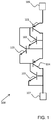
- FIG. 2 An example of an ESD protection device structure according to the present invention will now be described with reference to FIG. 2 .
- the structure described below with reference to FIG.2 may be considered to be an implementation of the simplified circuit diagram of FIG. 1 ..
- An ESD protection device 200 may comprise a semiconductor region 201 of a first type.
- the semiconductor region 201 may be an epitaxial region and in one example embodiment, may be a P type epitaxial region.
- a first, first type well 202 is formed within the semiconductor region 201 and within this first, first type well, a first, first type doped region 203 is formed.
- the first, first type doped region 203 serves as a first contact pad (106) of the device 200.
- the first, first type well 202 may be a P type well and the first ,first type doped region may be a P type doped region.
- a first, second type well 204 is formed within the semiconductor region 201.
- the first, first type well 202, the first, second type well 204 and the semiconductor region 201 constitute a first transistor 101 of a first conductivity type.
- this transistor 101 may be a PNP transistor.
- a second, first type well 205 which in one example may be a P well, is formed within the semiconductor region 201 and within this second, first type well 205 a first, second type doped region 206 and a second, first type doped region 207 are formed. These two doped regions 206, 207 may be joined together by a first conducting link 208 external to the semiconductor region 201.
- the first, second type doped region 206 may be an N type doped region and the second, first type doped region 207 may be a P type doped region.
- the first, second type well 204, the semiconductor region 201 and the first, second type doped region 206 constitute a second transistor 102 of a second conductivity type.
- this transistor 102 may be an NPN transistor.
- a second, second type well 209 is formed within the semiconductor region 201.
- this second, second type well 209 may be an N well.
- the first, second type well 204, the semiconductor region 201 and the second, second type well 209 constitute a third transistor 103 of a second conductivity type.
- this third transistor 100 may be an NPN transistor.
- a third, first type well 210 is formed within the semiconductor region 201.
- the third, first type well 210 may be a P well.
- a second, second type doped region 211 and a third, first type doped region 212 are formed within the third, first type doped region 210.
- the second, second type doped region 211 may be an N type doped region and the third, first type doped region may be a P type doped region. These two doped regions 211, 212 may be joined together by a second conducting link 213 external to the semiconductor region 201 to provide a second contact pad 107 of the device 200.
- the semiconductor region 201, the second, second type well 209 and the semiconductor region 201 constitute a fourth transistor 104 of a first conductivity type.
- his transistor 104 may comprise a PNP transistor.
- the second, second type well 209, the semiconductor region 201 and the second, second type doped region 211 constitute a fifth transistor 105 of a second conductivity type.
- this fifth transistor may comprise an NPN transistor.
- the semiconductor region 201 is provided with an insulating base 214 and sidewalls 215, 216 which may comprise deep trench isolation layers.
- a first, second type buried oxide layer 217 may be formed in a lower portion of the semiconductor region 201 and may overlap a lower portion of the first second type well 204.
- a second, second type buried oxide layer 218 may be formed in a lower portion of the semiconductor region 201 and may overlap a lower portion of the second, second type well 209. These two buried oxide layers 217, 218 may be provided in order to ensure that those parts of the semiconductor region 201 which lie under the first, second and third first type wells 202, 205, 210 are isolated from one another. Relying solely on the second type wells 204, 209 may be insufficient if these second type wells do not contact the insulating layer 214 below.
- the ESD protection device 200 may be mounted on a semiconductor substrate 221.
- upper surfaces of the first, first type well 202, the first ,second type well 204, the second, first type well 205, the second, second type well 209 and the third, first type well 210 may be separated from one another by shallow trench isolation layers 222.
- the first, first type well 202 may also include a third, second type doped region 219 which may be linked externally to the first, first type doped region 203 by an external conducting link 220.
- a bi-directional device may be provided which may function for a positive and a negative stress.
- the example embodiment of FIG.2 is, effectively, a merging of two, cascaded SCR stacks where in one embodiment, the second (central) first type well 205 may serve as the "P" part of an NPN bipolar transistor comprising part of a first SCR and may also serve as the "P" part of a PNP transistor comprising a part of a second SCR.
- the second (central) first type well 205 may serve as the "P" part of an NPN bipolar transistor comprising part of a first SCR and may also serve as the "P" part of a PNP transistor comprising a part of a second SCR.
- Example embodiments of an ESD protection device suitable for high voltage (typically 40 Volts) applications may be fabricated having a reduced silicon area compared with known devices
- the ESD protection device structure 200 of FIG.2 may be cascaded with a second identical ESD protection device structure 200 by operably coupling the second contact pad 107 of a first structure with the first contact pad 106 of the second structure.
- one or more additional SCR/Darlington stages may be formed in the semiconductor region 201 by replicating doped regions and wells.
- the ESD protection structure of FIG.2 may be modified by forming additional stages, each additional stage comprising a second type well and a first type well which has formed therein a doped region of a first type and a doped region of a second type.
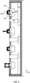
- FIG. 3 schematically shows a cross sectional view of an ESD protection device structure in accordance with such an embodiment and
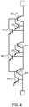
- FIG. 4 is a circuit diagram of this alternative embodiment.
- a second example of an ESD protection device structure 300 has certain features in common with the example of FIG.2 , the common features having the same reference numerals as those shown in FIG.2 and being formed in the same fashion.
- the ESD protection device structure 300 may comprise a third, second type well 301 formed within the semiconductor region 201.
- the second, second type well 209, the semiconductor region 201 and the third, second type well 301 may then comprise a sixth transistor 401 (see FIG. 4 ) of a second conductivity type.
- the semiconductor region 201, the third, second type well 301 and the semiconductor region 201 may comprise a seventh transistor 402 (see FIG. 4 ) of a first conductivity type.
- a fourth, first type well 302 may be formed within the semiconductor region 201 and may include a fourth, second type doped region 303 and a fourth, first type doped region 304.Tthe third, second type well 301, the semiconductor region 201 and the fourth, second type doped region 303 may comprise an eighth transistor 403 of a second conductivity type.
- a third, second type buried oxide layer 305 may be formed in a lower portion of the semiconductor region 201 and overlapping a lower portion of the third, first type well 301.
- An external conducting link 306 may be provided for linking the fourth doped regions 303, 304 of second and first types and may serve as a contact pad of the device structure 300 which may be grounded. In this way, an ESD protection circuit comprising two Darlington pairs and three series- connected silicon controlled rectifiers may be realised.
- FIG. 4 illustrates the circuit equivalent to the structure of FIG. 3 .
- the circuit of FIG. 4 comprises the five transistors 101, 102, 103, 104, 105 of FIG. 1 and an additional three transistors 401, 402, 403 mentioned above with reference to FIG. 3 .
- the additional transistors 401 and 403 may be of a second conductivity type and the additional transistor 402 may be of a first conductivity type.
- the first type transistor may be PNP transistors and the second type transistors may be NPN transistors.
- the first transistor 101 of a first conductivity type and the second transistor 102 of a second conductivity type may be operably coupled so that they constitute a first silicon controlled rectifier, SCR, configuration.
- the second transistor 102 of a second conductivity type and a third transistor 103 of a second conductivity type may be operably coupled so that they constitute a Darlington pair configuration.
- the fourth transistor 104 of a first conductivity type and the fifth transistor 105 of a second conductivity type may be operably coupled so that they constitute a second SCR configuration.
- the fifth transistor 105 of a second conductivity type and the sixth transistor 401 of a second conductivity type may be operably coupled so that they form another Darlington configuration.
- the seventh transistor 402 of a first conductivity type and the eighth transistor 403 of a second conductivity type may be operably coupled to form a further SCR configuration.
- the circuit 300 of FIG.3 may comprise three series-coupled SCRs.
- an emitter node of the first transistor 101 may serve as a first contact pad, or terminal 106 of the circuit 100.
- a base node of the first transistor 101 may be operably coupled to a collector node of the second transistor 102 and to the collector node of the third transistor 103.
- a collector node of the first transistor 101 may be operably coupled with a base node of the second transistor 102, a base node of the third transistor 103 and an emitter node of the fourth transistor 104.
- An emitter node of the second transistor 102 may be operably coupled to the base node of the third transistor 103.
- An emitter node of the third transistor 103 may be operably coupled to a base node of the fourth transistor 104 and to a collector node of the fifth transistor and to a collector node of the sixth transistor 302.
- a collector node of the fourth transistor 104 may be operably coupled with a base node of the fifth transistor 105 and may also be operably coupled with a base node of the sixth transistor 401 and an emitter node of the seventh transistor 402.
- An emitter node of the sixth transistor 401 may be operably coupled with a base node of the seventh transistor 402 and a collector node of the eighth transistor 403.
- a collector node of the seventh transistor 402 may be operably coupled with a base node of the eighth transistor 403 and to a contact pad 107 of the circuit 400 which may be grounded.
- An emitter node of the eighth transistor 403 may also be operably coupled with the (grounded) contact pad 107.
- FIG. 5 is a simplified flowchart of an example of a method 500 for manufacturing an ESD protection device structure, according to the present invention.
- the method may include providing an insulating layer below a semiconductor region of a first type and insulating side walls at the sides of the semiconductor region.
- the side walls may comprise deep trench isolation regions.
- the semiconductor region may be an epitaxial region.
- the semiconductor region may be P type.
- first, second and third first type wells 202,205 and 210 respectively are formed in the semiconductor region 201. These three wells are spaced apart from each other and may all extend the same depth into the semiconductor region. In one example embodiment, these first type wells may be P-type wells.
- first and second, second type wells 204, 209 respectively are formed in the semiconductor region 201 and in the intervening spaces between the first type wells.
- the wells may be separated from each other by shallow trench isolation regions.
- the second type wells may be N-type wells.
- the first, first type well, the first second type well and the semiconductor region constitute a transistor of a first type.
- This transistor comprises the first transistor 101 of FIG.1 .
- the first, second type well, the semiconductor region and the second, second type well constitute a transistor of a second type.
- This transistor may comprise the third transistor 103 of FIG.1 .
- the semiconductor region, second, second type well and the semiconductor region constitute a further transistor of a first type.
- This transistor comprises the fourth transistor 104 of FIG.1 .
- a first, first type doped region 203 is formed in the first, first type well.
- This first, first type doped region may serve as a contact pad (or terminal) of the device 200.
- the first, first type doped region may be a P-type doped region.
- a first, second type doped region 206 and a second, first type doped region 207 are formed in the second, first type well.
- the first, second type doped region may be an N-type doped region and the second, first type region may be a P-type doped region.
- the first, second type well, the semiconductor region and the first, second type doped region constitute a second transistor of a second type. This transistor comprises the transistor 102 of FIG. 1 .
- the first, second type doped region 206 and the second, first type doped region 207 may be operably coupled via an external conducting link 208.
- a second, second type doped region 211 and a third, first type doped region 212 are formed in the third, first type well.
- the second, second type doped region may be an N-type doped region and the third, first type region may be a P-type doped region.
- the second, second type well, the semiconductor region and the second, second type doped region constitute a fifth transistor of a second type. This transistor comprises the transistor 105 of FIG. 1 .
- the second, second type doped region and the third, first type doped region form a contact pad (or terminal) of the device and may be operably coupled together externally.
- the semiconductor regions described herein can be any semiconductor material or combinations of materials, such as gallium arsenide, silicon germanium, silicon-on-insulator (SOI), silicon, monocrystalline silicon, the like, and combinations of the above.
- connections as discussed herein may be any type of connection suitable to transfer signals from or to the respective nodes, units or devices, for example via intermediate devices. Accordingly, unless implied or stated otherwise, the connections may for example be direct connections or indirect connections.
- the connections may be illustrated or described in reference to being a single connection, a plurality of connections, unidirectional connections, or bidirectional connections. However, different embodiments may vary the implementation of the connections. For example, separate unidirectional connections may be used rather than bidirectional connections and vice versa.
- plurality of connections may be replaced with a single connection that transfers multiple signals serially or in a time multiplexed manner. Likewise, single connections carrying multiple signals may be separated out into various different connections carrying subsets of these signals. Therefore, many options exist for transferring signals.
- any arrangement of components to achieve the same functionality is effectively “associated” such that the desired functionality is achieved.
- any two components herein combined to achieve a particular functionality can be seen as “associated with” each other such that the desired functionality is achieved, irrespective of architectures or intermedial components.
- any two components so associated can also be viewed as being “operably connected,” or “operably coupled,” to each other to achieve the desired functionality.
- an ESD protection device structure may be implemented as circuitry implemented in a single integrated circuit or within a device which the circuit is protecting against ESD events. That is to say that an ESD protection device structure may be may be implemented in an integrated circuit.
- Such an integrated circuit may be a package containing one or more dies.
- an integrated circuit device may comprise one or more dies in a single package with electronic components provided on the dies that form the modules and which are connectable to other components outside the package through suitable connections such as pins of the package and bondwires between the pins and the dies.
- any reference signs placed between parentheses shall not be construed as limiting the claim.
- the word 'comprising' does not exclude the presence of other elements or steps then those listed in a claim.
- the terms "a” or "an,” as used herein, are defined as one or more than one.
Landscapes
- Semiconductor Integrated Circuits (AREA)
Claims (14)
- Eine elektrostatische Entladung Schutzvorrichtung Struktur (200), aufweisendeinen Halbleiterbereich (201) von einem ersten Typ,eine Isolierungsbasis (214), welche geformt ist unter dem Halbleiterbereich (201) und Seitenwänden (215, 216), welche isolieren den Halbleiterbereich (201);einen ersten ersten Typ von Quelle (202), welcher geformt ist innerhalb des Halbleiterbereiches (201) und umfasst einen ersten ersten Typ von dotiertem Bereich (203) zum Bereitstellen eines ersten Kontaktpads (106) von der Vorrichtung (200);einen ersten zweiten Typ von Quelle (204), welcher geformt ist innerhalb des Halbleiterbereiches (201) und separiert innerhalb des Halbleiterbereiches (201) einen ersten Teil von dem Halbleiterbereich (201), der enthält den ersten ersten Typ von Quelle (202), von einem weiteren Teil von dem Halbleiterbereich (201),
wobei der erste erste Typ von Quelle (202), der erste zweite Typ von Quelle (204) und der erste Teil von dem Halbleiterbereich (201) bilden einen ersten Transistor (101) von einem ersten Leitfähigkeitstyp;einen zweiten ersten Typ von Quelle (205), welcher geformt ist innerhalb der weiteren Teils von dem Halbleiterbereich (201) und umfasst einen ersten zweiten Typ von dotiertem Bereich (206) und einen zweiten ersten Typ von dotiertem Bereich (207),
wobei der erst zweite Typ von Quelle (204), der Halbleiterbereich (201) und der erste zweite Typ von dotiertem Bereich (206) bilden einen zweiten Transistor (102) von einem zweiten Leitfähigkeitstyp;einen zweiten zweiten Typ von Quelle (209), welcher geformt ist innerhalb des weiteren Teils von dem Halbleiterbereich (201) und separiert innerhalb des weiteren Teiles von dem Halbleiterbereich (201) einen zweiten Teil von dem Halbleiterbereich (201), der enthält den zweiten ersten Typ von Quelle (205), von einem dritten Teil von dem Halbleiterbereich (201),
wobei der erste zweite Typ von Quelle (204), der zweite Teil von dem Halbleiterbereich (201) und der zweite zweite Typ von Quelle (209) bilden einen dritten Transistor (103) von einem zweiten Leitfähigkeitstyp; undeinen dritten ersten Typ von Quelle (210), welcher geformt ist innerhalb des dritten Teils von dem Halbleiterbereich (201) und umfasst einen zweiten zweiten Typ von dotiertem Bereich (211) und einen dritten ersten Typ von dotiertem Bereich (212),
wobei der zweite Teil von dem Halbleiterbereich (201), der zweite zweite Typ von Quelle (209) und der dritte Teil von dem Halbleiterbereich (201) bilden einen vierten Transistor (104) von einem ersten Leitfähigkeitstyp,
wobei der zweite zweite Typ von Quelle (209), der dritte Teil von dem Halbleiterbereich (201) und der zweite zweite Typ von dotiertem Bereich (211) bilden einen fünften Transistor (105) von einem zweiten Leitfähigkeitstyp,
wobei der erste, zweite und dritte Teil von dem Halbleiterbereich (201), welche unterhalb des ersten, zweiten und dritten ersten Typs von Quellen liegen, isoliert sind von einander mittels des ersten und zweiten zweiten Typs von Quellen (204, 209), welche kontaktieren die Isolationsbasis (214),
wobei der erste Transistor (101) von dem ersten Leitfähigkeitstyp und der zweite Transistor (102) von dem zweiten Leitfähigkeitstyp betriebsfähig zusammengekoppelt sind und Formen einen ersten Silicon Controlled Receiver, SCR,
wobei der zweite Transistor (102) und der dritte Transistor (103) von dem zweiten Leitfähigkeitstyp betriebsfähig zusammengekoppelt sind und Formen ein Darlington Paar,
und
wobei der vierte Transistor (104) von dem ersten Leitfähigkeitstyp und der fünfte Transistor (105) von dem zweiten Leitfähigkeitstyp betriebsfähig zusammengekoppelt sind und Formen einen zweiten SCR, welcher betriebsfähig gekoppelt ist in Reihe mit dem ersten SCR. - Die ESD Schutzstruktur gemäß Anspruch 1, aufweisend
zumindest eine zusätzliche Stufe zum Bereitstellen von zusätzlichen Reihenverbundenen Transistoren,wobei eine zusätzliche Stufe aufweist einen dritten zweiten Typ von Quelle (301), welcher geformt ist innerhalb des dritten Teiles von dem Halbleiterbereich (201), damit Separieren eines vierten Teiles von dem Halbleiterbereich (201) von dem dritten Teil von dem Halbleiterbereich (201), und einen vierten ersten Typ von Quelle (302), welcher geformt ist innerhalb des vierten Teils von dem Halbleiterbereich (201) und aufweist einen vierten ersten Typ von dotiertem Bereich (304) und einen vierten zweiten Typ von dotiertem Bereich (303) geformt darin,wobei der dritte zweite Typ von Quelle (301) kontaktiert die Isolierungsbasis (214). - Die ESD Schutzstruktur (300) gemäß Anspruch 2, wobei:der zweite zweite Typ von Quelle (209), der vierte Teil von dem Halbleiterbereich (201) und der dritte zweite Typ von Quelle (301) aufweist einen sechsten Transistor (401) von einem zweiten Leitfähigkeitstyp,der dritte Teil von dem Halbleiterbereich (201), der dritte zweite Typ von Quelle (301) und vierte Teil von dem Halbleiterbereich (201) aufweist einen siebten Transistor (402) von einem ersten Leitfähigkeitstyp,der dritte zweite Typ von Quelle (301), der vierte Teil von dem Halbleiterbereich (201) und der vierte zweite Typ von dotiertem Bereich (303) aufweist einen achten Transistor (403) von einem zweiten Leitfähigkeitstyp.
- Die ESD Schutzvorrichtung Struktur (200) gemäß irgendeinem vorherigen Anspruch und umfassendeinen ersten zweiten Typ von verdeckter Oxidschicht (217), welche geformt ist in einem unteren Teil von dem Halbleiterbereich (201) und überlappt einen unteren Teil von dem ersten zweiten Typ von Quelle (204), undeinen zweiten zweiten Typ von verdeckter Oxidschicht (218), welche geformt ist in einem unteren Teil von dem Halbleiterbereich (201) und überlappt einen unteren Teil von dem zweiten zweiten Typ von Quelle (209).
- Die ESD Schutzvorrichtung Struktur (200) gemäß irgendeinem vorherigen Anspruch, wobei die Seitenwände (215, 216) aufweisen tiefe Graben Isolationsbereiche.
- Die ESD Schutzvorrichtung Struktur (200) gemäß irgendeinem vorherigen Anspruch und aufweisend untiefe Graben Isolationsbereiche (222), welche eingerichtet sind zum Separieren des ersten Typs von Quellen (202, 205, 210) von dem zweiten Typ von Quellen (204, 209).
- Die ESD Schutzvorrichtung Struktur (200) gemäß irgendeinem vorherigen Anspruch, wobei ein erster Typ ein P-Typ ist und ein zweiter Typ ein N-Typ ist und Transistoren von einem ersten Leitfähigkeitstyp PNP Transistoren sind und Transistoren von einem zweiten Leitfähigkeitstyp NPN Transistoren sind.
- Die ESD Schutzvorrichtung Struktur (200) gemäß irgendeinem vorherigen Anspruch, wobei der Halbleiterbereich (201) ein epiaxischer Bereich ist.
- Die ESD Schutzvorrichtung Struktur (200) gemäß irgendeinem vorherigen Anspruch, aufweisend
eine erste leitende Verbindung (208), welche betriebsfähig gekoppelt ist zwischen dem ersten zweiten Typ von dotiertem Bereich (206) und dem zweiten ersten Typ von dotiertem Bereich (207). - Die ESD Schutzvorrichtung Struktur (200) gemäß irgendeinem vorherigen Anspruch, aufweisend
ein zweite leitende Verbindung (213), welche betriebsfähig gekoppelt ist zwischen dem zweiten zweiten Typ von dotiertem Bereich (211) und dem dritten ersten Typ von dotiertem Bereich (212) zum Bereitstellen eines zweiten Kontaktpads (107) von der Vorrichtung (200). - Die ESD Schutzvorrichtung Struktur (200) gemäß irgendeinem vorherigen Anspruch, wobei der erste erste Typ von Quelle (202) umfasst einen dritten zweiten Typ von dotiertem Bereich (219), die Vorrichtung aufweisend
eine dritte leitende Verbindung (220), welche betriebsfähig gekoppelt ist zwischen dem dritten zweiten Typ von dotiertem Bereich (219) und dem ersten ersten Typ von dotiertem Bereich (203). - Die ESD Schutzvorrichtung Struktur (200) gemäß irgendeinem vorherigen Anspruch, wobei die ESD Schutzvorrichtung Struktur implementiert ist in einer integrierten Schaltkreisvorrichtung.
- Ein Verfahren (500) zum Herstellen einer ESD Schutzvorrichtung (200) gemäß irgendeinem vorherigen Anspruch, das Verfahren aufweisend
Formen von erstem, zweitem, drittem, viertem und fünftem Transistor (101, 102, 103, 104, 105), aufweisend:Formen von einer Isolierungsbasis (214) unter einem Halbleiterbereich von einem ersten Typ (201) und Seitenwänden (215, 216), welche den Halbleiterbereich isolieren (201);Formen (501) von einem ersten ersten Typ von Quelle (202) innerhalb des Halbleiterbereiches (201);Formen (502) von einem ersten zweiten Typ von Quelle (204) innerhalb des Halbleiterbereiches (201),
wobei der erste zweite Typ von Quelle (204) separiert innerhalb des Halbleiterbereiches (201) einen ersten Teil von dem Halbleiterbereich (201) enthaltend den ersten ersten Typ von Quelle (202) von einem weiteren Teil von dem Halbleiterbereich (201);Formen (501) von einem zweiten ersten Typ von Quelle (205) innerhalb des weiteren Teiles von dem Halbleiterbereich (201);Formen (502) von einem zweiten zweiten Typ von Quelle (209) innerhalb des anderen Teiles von dem Halbleiterbereich (201),
wobei der zweite zweite Typ von Quelle (209) separiert innerhalb des Halbleiterbereiches (201) einen zweiten Teil von dem Halbleiterbereich (201) enthaltend den zweiten ersten Typ von Quelle (205) von einem dritten Teil von dem Halbleiterbereich (201),
wobei der erste (204) und der zweite (209) zweite Typ von Quelle kontaktieren die Isolierungsbasis (214);Formen (501) von einem dritten ersten Typ von Quelle (210) innerhalb des dritten Teiles von dem Halbleiterbereich (201);Formen (503) von einem ersten ersten Typ von dotiertem Bereich (203) in dem ersten ersten Typ von Quelle (202) zum Formen eines ersten Kontaktpads (106) von der Vorrichtung;Formen (504) von einem ersten zweiten Typ von dotiertem Bereich (206) und einem zweiten ersten Typ von dotiertem Bereich (207) in dem zweiten ersten Typ von Quelle (205); undFormen (505) von einem zweiten zweiten Typ von dotiertem Bereich (211) und einem dritten ersten Typ von dotiertem Bereich (212) in dem dritten ersten Typ von Quelle (210),
wobei der erste Transistor (101) aufweist den ersten ersten Typ von Quelle (202), den ersten zweiten Typ von Quelle (204) und den ersten Teil von dem Halbleiterbereich (201),
wobei der zweite Transistor (102) aufweist den ersten zweiten Typ von Quelle (204), den Halbleiterbereich (201) und den ersten zweiten Typ von dotiertem Bereich (206),
wobei der dritte Transistor (103) aufweist den ersten zweiten Typ von Quelle (204), den zweiten Teil von dem Halbleiterbereich (201) und den zweiten zweiten Typ von Quelle (209),
wobei der vierte Transistor (104) aufweist den zweiten Teil von dem Halbleiterbereich (201), den zweiten zweiten Typ von Quelle (209) und den dritten Teil von dem Halbleiterbereich (201), und
wobei der fünfte Transistor (105) aufweist den zweiten zweiten Typ von Quelle (209), den dritten Teil von dem Halbleiterbereich (201) und den zweiten zweiten Typ von dotiertem Bereich (211). - Das Verfahren gemäß Anspruch 13, aufweisend
Formen (502) von untiefen Graben Isolationsbereichen (222), welche Separieren den ersten Typ von Quellen (202, 205, 210) von dem zweiten Typ von Quellen (204, 209).
Applications Claiming Priority (1)
| Application Number | Priority Date | Filing Date | Title |
|---|---|---|---|
| PCT/IB2013/002896 WO2015075495A1 (en) | 2013-11-22 | 2013-11-22 | Electrostatic discharge protection circuits and structures and methods of manufacture |
Publications (3)
| Publication Number | Publication Date |
|---|---|
| EP3072154A1 EP3072154A1 (de) | 2016-09-28 |
| EP3072154A4 EP3072154A4 (de) | 2017-08-02 |
| EP3072154B1 true EP3072154B1 (de) | 2020-01-08 |
Family
ID=53179022
Family Applications (1)
| Application Number | Title | Priority Date | Filing Date |
|---|---|---|---|
| EP13897742.6A Active EP3072154B1 (de) | 2013-11-22 | 2013-11-22 | Schaltungen zum schutz gegen elektrostatische entladung sowie strukturen und verfahren zur herstellung |
Country Status (3)
| Country | Link |
|---|---|
| US (1) | US10014289B2 (de) |
| EP (1) | EP3072154B1 (de) |
| WO (1) | WO2015075495A1 (de) |
Families Citing this family (7)
| Publication number | Priority date | Publication date | Assignee | Title |
|---|---|---|---|---|
| US10573639B2 (en) * | 2016-02-29 | 2020-02-25 | Globalfoundries Singapore Pte. Ltd. | Silicon controlled rectifier (SCR) based ESD protection device |
| EP3407385B1 (de) | 2017-05-23 | 2024-03-13 | NXP USA, Inc. | Zum schutz vor elektrostatischer entladung (esd) geeignetes halbleiterbauelement |
| EP3451379A1 (de) * | 2017-09-01 | 2019-03-06 | NXP USA, Inc. | Schutzschaltung gegen elektrostatische entladung mit einem bidirektionalen gesteuerten silicium-gleichrichter (scr) |
| US10608431B2 (en) | 2017-10-26 | 2020-03-31 | Analog Devices, Inc. | Silicon controlled rectifier dynamic triggering and shutdown via control signal amplification |
| US10580765B1 (en) * | 2018-12-02 | 2020-03-03 | Nanya Technology Corporation | Semiconductor structure for electrostatic discharge protection |
| CN111725201B (zh) * | 2019-03-20 | 2023-03-24 | 中芯国际集成电路制造(上海)有限公司 | Scr静电保护结构及其形成方法 |
| US11271099B2 (en) * | 2020-07-28 | 2022-03-08 | Amazing Microelectronic Corp. | Vertical bipolar transistor device |
Family Cites Families (16)
| Publication number | Priority date | Publication date | Assignee | Title |
|---|---|---|---|---|
| US5602409A (en) * | 1995-07-13 | 1997-02-11 | Analog Devices, Inc. | Bidirectional electrical overstress protection circuit for bipolar and bipolar-CMOS integrated circuits |
| US6768616B2 (en) * | 2001-03-16 | 2004-07-27 | Sarnoff Corporation | Electrostatic discharge protection structures for high speed technologies with mixed and ultra-low voltage supplies |
| US6717219B1 (en) | 2002-04-12 | 2004-04-06 | National Semiconductor Corporation | High holding voltage ESD protection structure for BiCMOS technology |
| US7825473B2 (en) * | 2005-07-21 | 2010-11-02 | Industrial Technology Research Institute | Initial-on SCR device for on-chip ESD protection |
| US8212320B1 (en) | 2006-03-15 | 2012-07-03 | National Semiconductor Corporation | High voltage tolerant ESD device |
| JP2010182727A (ja) * | 2009-02-03 | 2010-08-19 | Renesas Electronics Corp | 半導体装置 |
| EP2246885A1 (de) * | 2009-04-27 | 2010-11-03 | STmicroelectronics SA | Schutzvorrichtung für einen integrierten Schaltkreis gegen elektrostatische Entladungen |
| US8242566B2 (en) | 2010-01-19 | 2012-08-14 | Freescale Semiconductors, Inc. | Stacked ESD protection |
| US8648419B2 (en) * | 2010-01-20 | 2014-02-11 | Freescale Semiconductor, Inc. | ESD protection device and method |
| US8390092B2 (en) | 2010-11-12 | 2013-03-05 | Freescale Semiconductor, Inc. | Area-efficient high voltage bipolar-based ESD protection targeting narrow design windows |
| US8519434B2 (en) | 2011-03-22 | 2013-08-27 | Macronix International Co., Ltd. | Self detection device for high voltage ESD protection |
| US8526147B2 (en) | 2011-03-28 | 2013-09-03 | National Semiconductor Corporation | High voltage tolerant SCR clamp with avalanche diode triggering circuit |
| US20130020049A1 (en) | 2011-07-18 | 2013-01-24 | Architectural Applications P.C. | Architectural heat and moisture exchange |
| US9349716B2 (en) * | 2012-02-07 | 2016-05-24 | Sofics Bvba | Electrostatic discharge protection device |
| US8743516B2 (en) * | 2012-04-19 | 2014-06-03 | Freescale Semiconductor, Inc. | Sharing stacked BJT clamps for system level ESD protection |
| WO2014041388A1 (en) * | 2012-09-12 | 2014-03-20 | Freescale Semiconductor, Inc. | A semiconductor device and an integrated circuit comprising an esd protection device, esd protection devices and a method of manufacturing the semiconductor device |
-
2013
- 2013-11-22 US US15/037,714 patent/US10014289B2/en active Active
- 2013-11-22 WO PCT/IB2013/002896 patent/WO2015075495A1/en not_active Ceased
- 2013-11-22 EP EP13897742.6A patent/EP3072154B1/de active Active
Non-Patent Citations (1)
| Title |
|---|
| None * |
Also Published As
| Publication number | Publication date |
|---|---|
| US10014289B2 (en) | 2018-07-03 |
| US20160300832A1 (en) | 2016-10-13 |
| WO2015075495A1 (en) | 2015-05-28 |
| EP3072154A1 (de) | 2016-09-28 |
| EP3072154A4 (de) | 2017-08-02 |
Similar Documents
| Publication | Publication Date | Title |
|---|---|---|
| EP3072154B1 (de) | Schaltungen zum schutz gegen elektrostatische entladung sowie strukturen und verfahren zur herstellung | |
| US9825020B2 (en) | Semiconductor device and an integrated circuit comprising an ESD protection device, ESD protection devices and a method of manufacturing the semiconductor device | |
| US6919603B2 (en) | Efficient protection structure for reverse pin-to-pin electrostatic discharge | |
| US9209265B2 (en) | ESD devices comprising semiconductor fins | |
| US8455949B2 (en) | ESD protection element and ESD protection device for use in an electrical circuit | |
| US6861680B2 (en) | Silicon-on-insulator diodes and ESD protection circuits | |
| US9704849B2 (en) | Electrostatic discharge protection device structures and methods of manufacture | |
| US10263419B2 (en) | Transient voltage protection circuits, devices, and methods | |
| CN106030808B (zh) | 分段式npn垂直双极晶体管 | |
| CN101728820A (zh) | 用于触发双重scr esd保护的电源箝位电路和方法 | |
| KR20150071633A (ko) | 입출력 구조물을 위한 수직 나노와이어 트랜지스터 | |
| CN104576638B (zh) | Esd保护器件 | |
| US7471493B1 (en) | Fast and compact SCR ESD protection device for high-speed pins | |
| US20130285196A1 (en) | Esd protection circuit providing multiple protection levels | |
| CN112216690A (zh) | 具有低寄生电容的静电放电保护结构及其静电放电保护电路 | |
| CN114695341A (zh) | 具有高保持电压的低电容瞬态电压抑制器 | |
| CN105514103A (zh) | 静电放大保护器件 | |
| EP1359620A2 (de) | ESD-Schutz für rauschentkopplende Kondensatoren | |
| CN114551435B (zh) | 双向静电放电保护装置 | |
| US8941959B2 (en) | ESD protection apparatus | |
| EP4407683A1 (de) | Bipolartransistor mit isoliertem gate und datenübertragungssystem mit einem solchen bipolartransistor mit isoliertem gate | |
| US10361186B1 (en) | Suppression of parasitic discharge path in an electrical circuit | |
| CN210296371U (zh) | 半导体结构及其esd器件 | |
| CN110349948A (zh) | 静电放电保护装置及其应用 | |
| CN116387304A (zh) | 半导体器件和包括该半导体器件的esd保护器件 |
Legal Events
| Date | Code | Title | Description |
|---|---|---|---|
| PUAI | Public reference made under article 153(3) epc to a published international application that has entered the european phase |
Free format text: ORIGINAL CODE: 0009012 |
|
| 17P | Request for examination filed |
Effective date: 20160622 |
|
| AK | Designated contracting states |
Kind code of ref document: A1 Designated state(s): AL AT BE BG CH CY CZ DE DK EE ES FI FR GB GR HR HU IE IS IT LI LT LU LV MC MK MT NL NO PL PT RO RS SE SI SK SM TR |
|
| AX | Request for extension of the european patent |
Extension state: BA ME |
|
| RAP1 | Party data changed (applicant data changed or rights of an application transferred) |
Owner name: NXP USA, INC. |
|
| DAX | Request for extension of the european patent (deleted) | ||
| A4 | Supplementary search report drawn up and despatched |
Effective date: 20170630 |
|
| RIC1 | Information provided on ipc code assigned before grant |
Ipc: H01L 29/06 20060101ALI20170626BHEP Ipc: H01L 29/45 20060101ALI20170626BHEP Ipc: H01L 27/02 20060101ALI20170626BHEP Ipc: H01L 21/762 20060101ALI20170626BHEP Ipc: H01L 21/761 20060101ALI20170626BHEP Ipc: H01L 27/04 20060101AFI20170626BHEP Ipc: H01L 29/87 20060101ALI20170626BHEP |
|
| STAA | Information on the status of an ep patent application or granted ep patent |
Free format text: STATUS: EXAMINATION IS IN PROGRESS |
|
| 17Q | First examination report despatched |
Effective date: 20180928 |
|
| GRAP | Despatch of communication of intention to grant a patent |
Free format text: ORIGINAL CODE: EPIDOSNIGR1 |
|
| STAA | Information on the status of an ep patent application or granted ep patent |
Free format text: STATUS: GRANT OF PATENT IS INTENDED |
|
| INTG | Intention to grant announced |
Effective date: 20190705 |
|
| GRAJ | Information related to disapproval of communication of intention to grant by the applicant or resumption of examination proceedings by the epo deleted |
Free format text: ORIGINAL CODE: EPIDOSDIGR1 |
|
| STAA | Information on the status of an ep patent application or granted ep patent |
Free format text: STATUS: EXAMINATION IS IN PROGRESS |
|
| INTC | Intention to grant announced (deleted) | ||
| GRAP | Despatch of communication of intention to grant a patent |
Free format text: ORIGINAL CODE: EPIDOSNIGR1 |
|
| STAA | Information on the status of an ep patent application or granted ep patent |
Free format text: STATUS: GRANT OF PATENT IS INTENDED |
|
| GRAS | Grant fee paid |
Free format text: ORIGINAL CODE: EPIDOSNIGR3 |
|
| INTG | Intention to grant announced |
Effective date: 20191023 |
|
| GRAA | (expected) grant |
Free format text: ORIGINAL CODE: 0009210 |
|
| STAA | Information on the status of an ep patent application or granted ep patent |
Free format text: STATUS: THE PATENT HAS BEEN GRANTED |
|
| AK | Designated contracting states |
Kind code of ref document: B1 Designated state(s): AL AT BE BG CH CY CZ DE DK EE ES FI FR GB GR HR HU IE IS IT LI LT LU LV MC MK MT NL NO PL PT RO RS SE SI SK SM TR |
|
| REG | Reference to a national code |
Ref country code: GB Ref legal event code: FG4D |
|
| REG | Reference to a national code |
Ref country code: CH Ref legal event code: EP |
|
| REG | Reference to a national code |
Ref country code: DE Ref legal event code: R096 Ref document number: 602013065013 Country of ref document: DE |
|
| REG | Reference to a national code |
Ref country code: IE Ref legal event code: FG4D |
|
| REG | Reference to a national code |
Ref country code: AT Ref legal event code: REF Ref document number: 1223752 Country of ref document: AT Kind code of ref document: T Effective date: 20200215 |
|
| REG | Reference to a national code |
Ref country code: NL Ref legal event code: MP Effective date: 20200108 |
|
| REG | Reference to a national code |
Ref country code: LT Ref legal event code: MG4D |
|
| PG25 | Lapsed in a contracting state [announced via postgrant information from national office to epo] |
Ref country code: RS Free format text: LAPSE BECAUSE OF FAILURE TO SUBMIT A TRANSLATION OF THE DESCRIPTION OR TO PAY THE FEE WITHIN THE PRESCRIBED TIME-LIMIT Effective date: 20200108 Ref country code: LT Free format text: LAPSE BECAUSE OF FAILURE TO SUBMIT A TRANSLATION OF THE DESCRIPTION OR TO PAY THE FEE WITHIN THE PRESCRIBED TIME-LIMIT Effective date: 20200108 Ref country code: NL Free format text: LAPSE BECAUSE OF FAILURE TO SUBMIT A TRANSLATION OF THE DESCRIPTION OR TO PAY THE FEE WITHIN THE PRESCRIBED TIME-LIMIT Effective date: 20200108 Ref country code: PT Free format text: LAPSE BECAUSE OF FAILURE TO SUBMIT A TRANSLATION OF THE DESCRIPTION OR TO PAY THE FEE WITHIN THE PRESCRIBED TIME-LIMIT Effective date: 20200531 Ref country code: FI Free format text: LAPSE BECAUSE OF FAILURE TO SUBMIT A TRANSLATION OF THE DESCRIPTION OR TO PAY THE FEE WITHIN THE PRESCRIBED TIME-LIMIT Effective date: 20200108 Ref country code: NO Free format text: LAPSE BECAUSE OF FAILURE TO SUBMIT A TRANSLATION OF THE DESCRIPTION OR TO PAY THE FEE WITHIN THE PRESCRIBED TIME-LIMIT Effective date: 20200408 |
|
| PG25 | Lapsed in a contracting state [announced via postgrant information from national office to epo] |
Ref country code: SE Free format text: LAPSE BECAUSE OF FAILURE TO SUBMIT A TRANSLATION OF THE DESCRIPTION OR TO PAY THE FEE WITHIN THE PRESCRIBED TIME-LIMIT Effective date: 20200108 Ref country code: LV Free format text: LAPSE BECAUSE OF FAILURE TO SUBMIT A TRANSLATION OF THE DESCRIPTION OR TO PAY THE FEE WITHIN THE PRESCRIBED TIME-LIMIT Effective date: 20200108 Ref country code: HR Free format text: LAPSE BECAUSE OF FAILURE TO SUBMIT A TRANSLATION OF THE DESCRIPTION OR TO PAY THE FEE WITHIN THE PRESCRIBED TIME-LIMIT Effective date: 20200108 Ref country code: IS Free format text: LAPSE BECAUSE OF FAILURE TO SUBMIT A TRANSLATION OF THE DESCRIPTION OR TO PAY THE FEE WITHIN THE PRESCRIBED TIME-LIMIT Effective date: 20200508 Ref country code: BG Free format text: LAPSE BECAUSE OF FAILURE TO SUBMIT A TRANSLATION OF THE DESCRIPTION OR TO PAY THE FEE WITHIN THE PRESCRIBED TIME-LIMIT Effective date: 20200408 Ref country code: GR Free format text: LAPSE BECAUSE OF FAILURE TO SUBMIT A TRANSLATION OF THE DESCRIPTION OR TO PAY THE FEE WITHIN THE PRESCRIBED TIME-LIMIT Effective date: 20200409 |
|
| REG | Reference to a national code |
Ref country code: DE Ref legal event code: R097 Ref document number: 602013065013 Country of ref document: DE |
|
| PG25 | Lapsed in a contracting state [announced via postgrant information from national office to epo] |
Ref country code: RO Free format text: LAPSE BECAUSE OF FAILURE TO SUBMIT A TRANSLATION OF THE DESCRIPTION OR TO PAY THE FEE WITHIN THE PRESCRIBED TIME-LIMIT Effective date: 20200108 Ref country code: SK Free format text: LAPSE BECAUSE OF FAILURE TO SUBMIT A TRANSLATION OF THE DESCRIPTION OR TO PAY THE FEE WITHIN THE PRESCRIBED TIME-LIMIT Effective date: 20200108 Ref country code: CZ Free format text: LAPSE BECAUSE OF FAILURE TO SUBMIT A TRANSLATION OF THE DESCRIPTION OR TO PAY THE FEE WITHIN THE PRESCRIBED TIME-LIMIT Effective date: 20200108 Ref country code: SM Free format text: LAPSE BECAUSE OF FAILURE TO SUBMIT A TRANSLATION OF THE DESCRIPTION OR TO PAY THE FEE WITHIN THE PRESCRIBED TIME-LIMIT Effective date: 20200108 Ref country code: EE Free format text: LAPSE BECAUSE OF FAILURE TO SUBMIT A TRANSLATION OF THE DESCRIPTION OR TO PAY THE FEE WITHIN THE PRESCRIBED TIME-LIMIT Effective date: 20200108 Ref country code: DK Free format text: LAPSE BECAUSE OF FAILURE TO SUBMIT A TRANSLATION OF THE DESCRIPTION OR TO PAY THE FEE WITHIN THE PRESCRIBED TIME-LIMIT Effective date: 20200108 Ref country code: ES Free format text: LAPSE BECAUSE OF FAILURE TO SUBMIT A TRANSLATION OF THE DESCRIPTION OR TO PAY THE FEE WITHIN THE PRESCRIBED TIME-LIMIT Effective date: 20200108 |
|
| PLBE | No opposition filed within time limit |
Free format text: ORIGINAL CODE: 0009261 |
|
| STAA | Information on the status of an ep patent application or granted ep patent |
Free format text: STATUS: NO OPPOSITION FILED WITHIN TIME LIMIT |
|
| REG | Reference to a national code |
Ref country code: AT Ref legal event code: MK05 Ref document number: 1223752 Country of ref document: AT Kind code of ref document: T Effective date: 20200108 |
|
| 26N | No opposition filed |
Effective date: 20201009 |
|
| PG25 | Lapsed in a contracting state [announced via postgrant information from national office to epo] |
Ref country code: AT Free format text: LAPSE BECAUSE OF FAILURE TO SUBMIT A TRANSLATION OF THE DESCRIPTION OR TO PAY THE FEE WITHIN THE PRESCRIBED TIME-LIMIT Effective date: 20200108 Ref country code: IT Free format text: LAPSE BECAUSE OF FAILURE TO SUBMIT A TRANSLATION OF THE DESCRIPTION OR TO PAY THE FEE WITHIN THE PRESCRIBED TIME-LIMIT Effective date: 20200108 |
|
| PG25 | Lapsed in a contracting state [announced via postgrant information from national office to epo] |
Ref country code: PL Free format text: LAPSE BECAUSE OF FAILURE TO SUBMIT A TRANSLATION OF THE DESCRIPTION OR TO PAY THE FEE WITHIN THE PRESCRIBED TIME-LIMIT Effective date: 20200108 Ref country code: SI Free format text: LAPSE BECAUSE OF FAILURE TO SUBMIT A TRANSLATION OF THE DESCRIPTION OR TO PAY THE FEE WITHIN THE PRESCRIBED TIME-LIMIT Effective date: 20200108 |
|
| PG25 | Lapsed in a contracting state [announced via postgrant information from national office to epo] |
Ref country code: MC Free format text: LAPSE BECAUSE OF FAILURE TO SUBMIT A TRANSLATION OF THE DESCRIPTION OR TO PAY THE FEE WITHIN THE PRESCRIBED TIME-LIMIT Effective date: 20200108 |
|
| REG | Reference to a national code |
Ref country code: CH Ref legal event code: PL |
|
| GBPC | Gb: european patent ceased through non-payment of renewal fee |
Effective date: 20201122 |
|
| PG25 | Lapsed in a contracting state [announced via postgrant information from national office to epo] |
Ref country code: LU Free format text: LAPSE BECAUSE OF NON-PAYMENT OF DUE FEES Effective date: 20201122 |
|
| REG | Reference to a national code |
Ref country code: BE Ref legal event code: MM Effective date: 20201130 |
|
| PG25 | Lapsed in a contracting state [announced via postgrant information from national office to epo] |
Ref country code: CH Free format text: LAPSE BECAUSE OF NON-PAYMENT OF DUE FEES Effective date: 20201130 Ref country code: LI Free format text: LAPSE BECAUSE OF NON-PAYMENT OF DUE FEES Effective date: 20201130 |
|
| PG25 | Lapsed in a contracting state [announced via postgrant information from national office to epo] |
Ref country code: FR Free format text: LAPSE BECAUSE OF NON-PAYMENT OF DUE FEES Effective date: 20201130 Ref country code: IE Free format text: LAPSE BECAUSE OF NON-PAYMENT OF DUE FEES Effective date: 20201122 |
|
| PG25 | Lapsed in a contracting state [announced via postgrant information from national office to epo] |
Ref country code: GB Free format text: LAPSE BECAUSE OF NON-PAYMENT OF DUE FEES Effective date: 20201122 |
|
| PG25 | Lapsed in a contracting state [announced via postgrant information from national office to epo] |
Ref country code: TR Free format text: LAPSE BECAUSE OF FAILURE TO SUBMIT A TRANSLATION OF THE DESCRIPTION OR TO PAY THE FEE WITHIN THE PRESCRIBED TIME-LIMIT Effective date: 20200108 Ref country code: MT Free format text: LAPSE BECAUSE OF FAILURE TO SUBMIT A TRANSLATION OF THE DESCRIPTION OR TO PAY THE FEE WITHIN THE PRESCRIBED TIME-LIMIT Effective date: 20200108 Ref country code: CY Free format text: LAPSE BECAUSE OF FAILURE TO SUBMIT A TRANSLATION OF THE DESCRIPTION OR TO PAY THE FEE WITHIN THE PRESCRIBED TIME-LIMIT Effective date: 20200108 |
|
| PG25 | Lapsed in a contracting state [announced via postgrant information from national office to epo] |
Ref country code: MK Free format text: LAPSE BECAUSE OF FAILURE TO SUBMIT A TRANSLATION OF THE DESCRIPTION OR TO PAY THE FEE WITHIN THE PRESCRIBED TIME-LIMIT Effective date: 20200108 Ref country code: AL Free format text: LAPSE BECAUSE OF FAILURE TO SUBMIT A TRANSLATION OF THE DESCRIPTION OR TO PAY THE FEE WITHIN THE PRESCRIBED TIME-LIMIT Effective date: 20200108 |
|
| PG25 | Lapsed in a contracting state [announced via postgrant information from national office to epo] |
Ref country code: BE Free format text: LAPSE BECAUSE OF NON-PAYMENT OF DUE FEES Effective date: 20201130 |
|
| P01 | Opt-out of the competence of the unified patent court (upc) registered |
Effective date: 20230725 |
|
| REG | Reference to a national code |
Ref country code: DE Ref legal event code: R079 Ref document number: 602013065013 Country of ref document: DE Free format text: PREVIOUS MAIN CLASS: H01L0027040000 Ipc: H10D0084000000 |
|
| PGFP | Annual fee paid to national office [announced via postgrant information from national office to epo] |
Ref country code: DE Payment date: 20251022 Year of fee payment: 13 |