EP3407385B1 - Zum schutz vor elektrostatischer entladung (esd) geeignetes halbleiterbauelement - Google Patents
Zum schutz vor elektrostatischer entladung (esd) geeignetes halbleiterbauelement Download PDFInfo
- Publication number
- EP3407385B1 EP3407385B1 EP17305609.4A EP17305609A EP3407385B1 EP 3407385 B1 EP3407385 B1 EP 3407385B1 EP 17305609 A EP17305609 A EP 17305609A EP 3407385 B1 EP3407385 B1 EP 3407385B1
- Authority
- EP
- European Patent Office
- Prior art keywords
- substrate
- deep well
- doped region
- patterned
- buried layer
- Prior art date
- Legal status (The legal status is an assumption and is not a legal conclusion. Google has not performed a legal analysis and makes no representation as to the accuracy of the status listed.)
- Active
Links
Images



Classifications
-
- H—ELECTRICITY
- H10—SEMICONDUCTOR DEVICES; ELECTRIC SOLID-STATE DEVICES NOT OTHERWISE PROVIDED FOR
- H10D—INORGANIC ELECTRIC SEMICONDUCTOR DEVICES
- H10D89/00—Aspects of integrated devices not covered by groups H10D84/00 - H10D88/00
- H10D89/60—Integrated devices comprising arrangements for electrical or thermal protection, e.g. protection circuits against electrostatic discharge [ESD]
-
- H—ELECTRICITY
- H10—SEMICONDUCTOR DEVICES; ELECTRIC SOLID-STATE DEVICES NOT OTHERWISE PROVIDED FOR
- H10D—INORGANIC ELECTRIC SEMICONDUCTOR DEVICES
- H10D18/00—Thyristors
-
- H—ELECTRICITY
- H10—SEMICONDUCTOR DEVICES; ELECTRIC SOLID-STATE DEVICES NOT OTHERWISE PROVIDED FOR
- H10D—INORGANIC ELECTRIC SEMICONDUCTOR DEVICES
- H10D18/00—Thyristors
- H10D18/01—Manufacture or treatment
-
- H—ELECTRICITY
- H10—SEMICONDUCTOR DEVICES; ELECTRIC SOLID-STATE DEVICES NOT OTHERWISE PROVIDED FOR
- H10D—INORGANIC ELECTRIC SEMICONDUCTOR DEVICES
- H10D62/00—Semiconductor bodies, or regions thereof, of devices having potential barriers
- H10D62/10—Shapes, relative sizes or dispositions of the regions of the semiconductor bodies; Shapes of the semiconductor bodies
- H10D62/102—Constructional design considerations for preventing surface leakage or controlling electric field concentration
- H10D62/103—Constructional design considerations for preventing surface leakage or controlling electric field concentration for increasing or controlling the breakdown voltage of reverse-biased devices
- H10D62/105—Constructional design considerations for preventing surface leakage or controlling electric field concentration for increasing or controlling the breakdown voltage of reverse-biased devices by having particular doping profiles, shapes or arrangements of PN junctions; by having supplementary regions, e.g. junction termination extension [JTE]
- H10D62/108—Constructional design considerations for preventing surface leakage or controlling electric field concentration for increasing or controlling the breakdown voltage of reverse-biased devices by having particular doping profiles, shapes or arrangements of PN junctions; by having supplementary regions, e.g. junction termination extension [JTE] having localised breakdown regions, e.g. built-in avalanching regions
-
- H—ELECTRICITY
- H10—SEMICONDUCTOR DEVICES; ELECTRIC SOLID-STATE DEVICES NOT OTHERWISE PROVIDED FOR
- H10D—INORGANIC ELECTRIC SEMICONDUCTOR DEVICES
- H10D62/00—Semiconductor bodies, or regions thereof, of devices having potential barriers
- H10D62/10—Shapes, relative sizes or dispositions of the regions of the semiconductor bodies; Shapes of the semiconductor bodies
- H10D62/113—Isolations within a component, i.e. internal isolations
- H10D62/114—PN junction isolations
-
- H—ELECTRICITY
- H10—SEMICONDUCTOR DEVICES; ELECTRIC SOLID-STATE DEVICES NOT OTHERWISE PROVIDED FOR
- H10D—INORGANIC ELECTRIC SEMICONDUCTOR DEVICES
- H10D8/00—Diodes
- H10D8/80—PNPN diodes, e.g. Shockley diodes or break-over diodes
-
- H—ELECTRICITY
- H10—SEMICONDUCTOR DEVICES; ELECTRIC SOLID-STATE DEVICES NOT OTHERWISE PROVIDED FOR
- H10D—INORGANIC ELECTRIC SEMICONDUCTOR DEVICES
- H10D89/00—Aspects of integrated devices not covered by groups H10D84/00 - H10D88/00
- H10D89/60—Integrated devices comprising arrangements for electrical or thermal protection, e.g. protection circuits against electrostatic discharge [ESD]
- H10D89/601—Integrated devices comprising arrangements for electrical or thermal protection, e.g. protection circuits against electrostatic discharge [ESD] for devices having insulated gate electrodes, e.g. for IGFETs or IGBTs
- H10D89/611—Integrated devices comprising arrangements for electrical or thermal protection, e.g. protection circuits against electrostatic discharge [ESD] for devices having insulated gate electrodes, e.g. for IGFETs or IGBTs using diodes as protective elements
-
- H—ELECTRICITY
- H10—SEMICONDUCTOR DEVICES; ELECTRIC SOLID-STATE DEVICES NOT OTHERWISE PROVIDED FOR
- H10D—INORGANIC ELECTRIC SEMICONDUCTOR DEVICES
- H10D89/00—Aspects of integrated devices not covered by groups H10D84/00 - H10D88/00
- H10D89/60—Integrated devices comprising arrangements for electrical or thermal protection, e.g. protection circuits against electrostatic discharge [ESD]
- H10D89/601—Integrated devices comprising arrangements for electrical or thermal protection, e.g. protection circuits against electrostatic discharge [ESD] for devices having insulated gate electrodes, e.g. for IGFETs or IGBTs
- H10D89/711—Integrated devices comprising arrangements for electrical or thermal protection, e.g. protection circuits against electrostatic discharge [ESD] for devices having insulated gate electrodes, e.g. for IGFETs or IGBTs using bipolar transistors as protective elements
- H10D89/713—Integrated devices comprising arrangements for electrical or thermal protection, e.g. protection circuits against electrostatic discharge [ESD] for devices having insulated gate electrodes, e.g. for IGFETs or IGBTs using bipolar transistors as protective elements including a PNP transistor and a NPN transistor, wherein each of said transistors has its base region coupled to the collector region of the other transistor, e.g. silicon controlled rectifier [SCR] devices
-
- H—ELECTRICITY
- H10—SEMICONDUCTOR DEVICES; ELECTRIC SOLID-STATE DEVICES NOT OTHERWISE PROVIDED FOR
- H10P—GENERIC PROCESSES OR APPARATUS FOR THE MANUFACTURE OR TREATMENT OF DEVICES COVERED BY CLASS H10
- H10P30/00—Ion implantation into wafers, substrates or parts of devices
- H10P30/20—Ion implantation into wafers, substrates or parts of devices into semiconductor materials, e.g. for doping
- H10P30/22—Ion implantation into wafers, substrates or parts of devices into semiconductor materials, e.g. for doping using masks
-
- H—ELECTRICITY
- H10—SEMICONDUCTOR DEVICES; ELECTRIC SOLID-STATE DEVICES NOT OTHERWISE PROVIDED FOR
- H10P—GENERIC PROCESSES OR APPARATUS FOR THE MANUFACTURE OR TREATMENT OF DEVICES COVERED BY CLASS H10
- H10P95/00—Generic processes or apparatus for manufacture or treatments not covered by the other groups of this subclass
- H10P95/90—Thermal treatments, e.g. annealing or sintering
-
- H—ELECTRICITY
- H10—SEMICONDUCTOR DEVICES; ELECTRIC SOLID-STATE DEVICES NOT OTHERWISE PROVIDED FOR
- H10W—GENERIC PACKAGES, INTERCONNECTIONS, CONNECTORS OR OTHER CONSTRUCTIONAL DETAILS OF DEVICES COVERED BY CLASS H10
- H10W10/00—Isolation regions in semiconductor bodies between components of integrated devices
- H10W10/01—Manufacture or treatment
- H10W10/031—Manufacture or treatment of isolation regions comprising PN junctions
-
- H—ELECTRICITY
- H10—SEMICONDUCTOR DEVICES; ELECTRIC SOLID-STATE DEVICES NOT OTHERWISE PROVIDED FOR
- H10W—GENERIC PACKAGES, INTERCONNECTIONS, CONNECTORS OR OTHER CONSTRUCTIONAL DETAILS OF DEVICES COVERED BY CLASS H10
- H10W10/00—Isolation regions in semiconductor bodies between components of integrated devices
- H10W10/30—Isolation regions comprising PN junctions
-
- H—ELECTRICITY
- H10—SEMICONDUCTOR DEVICES; ELECTRIC SOLID-STATE DEVICES NOT OTHERWISE PROVIDED FOR
- H10W—GENERIC PACKAGES, INTERCONNECTIONS, CONNECTORS OR OTHER CONSTRUCTIONAL DETAILS OF DEVICES COVERED BY CLASS H10
- H10W20/00—Interconnections in chips, wafers or substrates
- H10W20/01—Manufacture or treatment
- H10W20/021—Manufacture or treatment of interconnections within wafers or substrates
-
- H—ELECTRICITY
- H10—SEMICONDUCTOR DEVICES; ELECTRIC SOLID-STATE DEVICES NOT OTHERWISE PROVIDED FOR
- H10W—GENERIC PACKAGES, INTERCONNECTIONS, CONNECTORS OR OTHER CONSTRUCTIONAL DETAILS OF DEVICES COVERED BY CLASS H10
- H10W20/00—Interconnections in chips, wafers or substrates
- H10W20/20—Interconnections within wafers or substrates, e.g. through-silicon vias [TSV]
Definitions
- This disclosure relates generally to integrated circuits, and more specifically, to semiconductor devices suitable for electrostatic discharge (ESD) protection.
- ESD electrostatic discharge
- Electrostatic discharge (ESD) is a problem in the utilization, manufacturing and design of the semiconductor devices.
- the integrated circuits manufactured on the semiconductor device can be damaged when ESD events are received from other circuits coupled to the semiconductor device or from people or machinery and tools touching the semiconductor device.
- the integrated circuit may receive a charge which leads to relatively large currents during a relatively short period of time.
- the large current until several amps during tens of nanoseconds
- the voltage inside the IC increases. If the resulting voltage, current, power or energy exceed a maximum capability of the circuits then it may create irreparable damage to the integrated circuit.
- ESD protection circuitries that are able to conduct the charge of an ESD event to, for example, the ground without causing irreparable damage to the integrated circuit.
- ESD protection circuits are typically arranged near the I/O pads of the integrated circuit and are configured to conduct the charge of the ESD event directly to the ground before the current may reach the vulnerable portions of the integrated circuit.
- US5883414 describes an integrated circuit with a passive component and an ESD device which comprises comprises: a P substrate; an N+ buried layer implanted in the P substrate; a cathode coupled to the N+ buried layer with an N area formed between the cathode and the N+ buried layer; an anode coupled to the N+ buried layer with a P area formed between the anode and the N+ buried layer; and a first P+ buried layer implanted in the N+ buried layer and below the P area to form a Zener diode.
- the accuracy of the breakdown voltage (BV) and its location within an ESD device impacts the reliability of the ESD device.
- the BV adjustment of an ESD device is achieved with the modulation of the lateral spacing between the n-doped and p-doped layers.
- This lateral location of the BV results in the greatest current density/flow during avalanche being located at the closest spacing between the n-doped and p-doped layers near the top surface of the device.
- This hot spot location prevents the ESD device from sustaining sufficient Gun stress and thus from providing sufficient protection. Therefore, a need exists for an ESD device which allows for the proper accuracy and location of the BV to allow for improved protection of an integrated circuit.
- the present invention consists of a device as defined in claim 1 and a method as defined in claim 10.
- Preferred embodiments are defined in the dependent claims. It is illustrated by way of example and is not limited by the accompanying figures, in which like references indicate similar elements. Elements in the figures are illustrated for simplicity and clarity and have not necessarily been drawn to scale.
- an ESD device is formed having a vertical location of the breakdown area within a p-n junction. In this manner, current flows vertically downward, toward the substrate, from the p-n junction. This vertical location of the BV allows a finer adjustment of the BV than currently allowed by the lateral location of the BV. In one embodiment, by controlling a spacing between two adjacent openings in a mask used to form an N-type buried layer of the ESD device, the vertical BV for the resulting p-n junction can be accurately defined.
- FIG. 1 illustrates, in cross-sectional form, an ESD device 10 at a stage in processing.
- Device 10 includes a substrate 12, which can be any semiconductor material or combinations of materials, such as gallium arsenide, silicon germanium, silicon, monocrystalline silicon, the like, or combinations thereof.
- An insulator layer 14 is located over substrate 12.
- insulator layer 14 is an oxide layer and may be referred to as buried oxide (BOX) layer 14 and may have a thickness of 300 nanometers.
- a P-type epitaxial silicon (P-epi) layer 16 is located over BOX layer 14.
- layer 16 has a thickness of 1500 nanometers and a doping level of 2e15 atoms/cm 3 .
- device 10 corresponds to a semiconductor-on-insulator (SOI) device, with a semiconductor layer (silicon layer 26) over an insulator (BOX layer 14).
- An insulator layer 18 is located over P-epi layer 16.
- the thickness of layer 18 may be, for example, 15 nanometers.
- a patterned masking layer 20 is formed over layer 18 which has a portion 20 located between mask openings 19 and 21. Patterned masking layer 20 may be formed of photoresist.
- An implant 20 is performed using masking layer 20, in which the implant through openings 19 and 21 and layer 18 result in highly doped N-type implant regions 24 and 26, respectively, within P-epi layer 16, which correspond to portions of a highly doped N-type buried layer (NBL).
- the implants to form N-type regions 24 and 26 may include antimony, arsenic, or phosphorous.
- width 28 of portion 20 defines a lateral distance by which region 26 is spaced from region 24 in P-epi layer 16. Therefore, by controlling width 28, the lateral distance between regions 24 and 26 is affected.
- patterned masking layer 20 is removed.
- FIG. 2 illustrates, in cross-sectional form, ESD device 10 at a subsequent stage in processing.
- a second P-type epitaxial (P-epi) layer 30 is formed over P-epi layer 16.
- P-epi layer 30 has a thickness in a range of about 3000 nm to 5000 nm.
- An implant anneal is performed to drive the dopants of regions 24 and 26 further into P-epi layer 16 to result in an NBL 41 having a first portion 42 corresponding to annealed region 24 and a second portion 44 corresponding to annealed region 26.
- the distance after anneal between portions 42 and 44 is less than a distance between portions 24 and 26.
- Each portion 42 and 44 has a first end and a second end, wherein the first ends have a smaller vertical (with respect to substrate 12) cross-section than the second ends.
- the first ends of portions 42 and 44 are adjacent each other, and the distance between them, after anneal, is dependent upon width 28 of portion 20 described above.
- the NBL may also be referred to as a patterned buried layer. As will be discussed below, the spacing between portion 42 and 44 will determine the BV of device 10.
- shallow trench isolation (STI) regions 32 are formed within P-epi layer 30.
- An insulating layer 34 is formed over P-epi layer 30 and STI regions 32.
- a patterned masking layer 36 is then formed over P-epi layer 30 and insulating layer 34 having an opening 35 which exposes a region of P-epi layer 30 between STI regions 32. Note that width 39 of opening 35 is greater than width 28.
- Patterned masking layer 36 may be formed of photoresist.
- An implant 38 is performed using masking layer 36, in which the implant through opening 35 and layer 34 result in a medium doped P-type implant region 40, also referred to as Pwell 40 (or a deep well).
- implant 38 has a higher dopant concentration that P-epi layer 30.
- implant 38 may include a boron implant at an energy within a range of 5 keV to 500 keV. After implant 38, patterned masking layer 36 is removed.
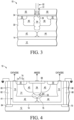
- FIG. 3 illustrates, in cross-sectional form, ESD device 10 at a subsequent stage in processing in which a vertical p-n junction is formed.
- a patterned masking layer 50 is formed over P-epi layer 30 and insulating layer 34 having an opening 51 which exposes a region of P-epi layer 30 within Pwell 40. Opening 51 is aligned with a center of previous portion 20 of patterned masking layer 28. Opening 51 has a width 58 which is smaller than widths 28 and 39.
- An implant 52 is performed using masking layer 50, in which the implant through opening 51 and layer 34 results in a highly doped P-type low voltage well (LVP) 54 (also referred to as a patterned doped region).
- LVP highly doped P-type low voltage well
- LVP 54 extends deeper into P-epi 30 than Pwell 40 and is more heavily doped than Pwell 40.
- a bottom tip 53 of LVP 54 is located directly over the first ends of portions 42 and 44, and the proximity of the bottom tip of LVP 54 to portions 42 and 44 of NBL 41 ensures a deep p-n junction.
- an anneal is performed to drive the dopants into P-epi layer 30. Note that the combination of P-epi layers 16 and 30 are referred to as P-epi layer 31.
- implant 52 may include several different implants with high energy.
- implant 52 may include a boron implant at an energy within a range of 5 keV to 1 MeV. This results in a vertical doping distribution of LVP 54 from the top of LVP 54 to the bottom tip of LVP 54.
- LPV 54 is more heavily doped than Pwell 40, and Pwell 40 is more heavily doped than P-epi layer 30.
- the dopant concentration of P-epi layer 30 is 2e15 dopants/cm 3
- the highest doping levels of the dopant distribution of LVP 54 is in a range of 5e17 and 8e17 dopants/cm 3
- the highest doping levels of the dopant distribution of Pwell 40 is about 4e17 dopants/cm 3 .
- FIG. 4 illustrates, in cross-sectional form, a wider cross-section of the ESD device 10 at a subsequent stage in processing.
- DPN deep N well
- DTI deep trench isolation
- DPN region 70 extends vertically from the top surface of P-epi layer 30 to NBL 41, contacting portion 42.
- DPN region 72 extends vertically from the top surface of P-epi layer 30 to NBL 41, contacting portion 44.
- DPN regions 70 and 72 are located at the outer sides and under a portion of STI regions 32, such that STI regions 32 are located between DPN regions 70 and 72.
- DPN regions 70 and 72 and portions 42 and 44 form an isolation structure around P-epi layer 31, Pwell 40, and LVP 54.
- Adjacent DPN 70 is DTI region 60 which provides an N-type polysilicon contact region 62 extending vertically from a top surface of DTI 60 to contact substrate 12 at a heavily doped N-type region 64 formed in substrate 12.
- a shallow heavily doped P-type region 68 (also referred to as a shallow doped layer) is formed in P-epi layer 31, in Pwell 40 and LPV 54, and extends less into P-epi layer 31 than Pwell 40 and LVP 54.
- P-type doped region 68 serves as an anode terminal of ESD device 10.
- DPN regions 70 and 72 serve as cathode terminals of ESD device 10. Therefore, device 10 includes a pair of diodes. Adjacent DPN 72 is DTI region 66 which provides an N-type polysilicon contact region 68 extending vertically from a top surface of DTI 66 to contact substrate 12 at a heavily doped N-type region 70 formed in substrate 12. Contact regions 62 and 68 provide a ground connection for substrate 12. DTI regions 60 and 66 laterally isolate p-n junction 75 and device 10 from neighboring devices.
- p-n junction 75 corresponds to the location of the BV of device 10.
- P-n junction 75 corresponds to the top p-n junction between portions 42, 44, and layer 31.
- Distance (d) 74 between DPN 70 and Pwell 40 should be high enough to ensure maximum electric field in the bottom of the p-n junction between LVP 54 and NBL 41.
- the diode p-n junction 75 is formed by LVP 54 and NBL 42 and 44, at the point where portions 42 and 44 are closest to each other.
- the bottom tip of LVP 54 is located directly over NBL portions 42 and 44 at the point where their first ends are closest to each other.
- the BV can be modulated and adjusted using different values for width 28 (described above in reference to FIG. 1 ) which is aligned to width 58 of the mask used to form LVP 54. With the BV location at p-n junction 75, the current density/flow during BV occurs vertically (with respect to substrate 12) from the p-n junction down through NBL 41 to DPN region 70.
- p-n junction 75 being located under LVP 54 (and under the location of opening 51 used to form LVP 54), a smaller ESD device can be formed while having the ability to adjust, with good precision and smaller dispersion, the BV of the device. This is due to the vertical location of the impact ionization in the bottom of the junction (at p-n junction 75) due to the vertical LVP doping distribution stacked over the spacing between portions 42 and 44. This vertical design may also allow ESD protection with reduced voltage overshoot during fast ESD events.
- ESD protection circuit includes a bi-directional Silicon Controlled Rectifier (SCR) coupled with a PNP transistor.
- SCR Silicon Controlled Rectifier
- a SCR or a thyristor
- NPN NPN
- SCR devices can be stacked to offer higher voltage protection.
- the spacing between the Pwell and DPN layers in the SCR, which form the base/collector junction define the BV and triggering voltage of the ESD circuit.
- FIG. 5 illustrates, in cross-sectional form, a semiconductor device 100 of an integrated circuit in accordance with an alternate embodiment of the present invention.
- a bi-directional mono-stack SCR ESD protection device can be formed which is coupled to an I/O pad of the integrated circuit.
- the I/O pad is configured to receive or provide an input/output signal.
- Device 100 includes a substrate 102 and an insulating layer 104 on substrate 102. Note that the descriptions provided above with respect to substrate 12 and insulating layer 14 apply to substrate 102 and insulating layer 104.
- a P-epi layer 105 is located on insulating layer 104.
- NBL 106 is formed in P-epi layer 105, over insulating layer 104.
- DPN regions 154 and 156 are formed in P-epi layer 105 extending vertically from the top surface of P-epi layer 105 down to NBL 106.
- Adjacent DPN 156 is a DTI 160 which extends vertically down to contact substrate 102, and within DTI 160 is an N-type polysilicon contact region 162 extending vertically from a contact 164 located on a top surface of DTI 160 to contact substrate 102 at a heavily doped N-type region 166 formed in n-type substrate 102.
- Contact region 162 provides a ground connection for substrate 102.
- DTI regions 160 laterally isolate device 100 from neighboring devices.
- Pwells 128 and 134 are formed in P-epi layer 105.
- NBL 106 includes portions 108 and 110, similar to portions 42 and 44, and portions 112 and 114, similar to portions 42 and 44.
- Pwell 128 is formed over NBL 106, and LVP 130 is formed within the width of Pwell 128 and extends further into P-epi layer 105 than Pwell 128.
- a doped p-n junction 138 is formed by LPV 130 and NBL 108 and 110, at the point where portions 108 and 110 are closest to each other.
- Pwell 134 is formed over NBL 106, and LVP 136 is formed within the width of Pwell 134 and extends further into P-epi layer 105 than Pwell 134.
- a doped p-n junction 140 is formed by LVP 136 and NBL 112 and 114, at the point where portions 112 and 114 are closest to each other.
- Pwell 40, LVP 54, and NBL portions 42 and 44 also apply to Pwell 128, LVP 130, and NBL portions 108 and 110 as well as to Pwell 134, LVP 136, and NBL portions 112 and 114.
- width 132 corresponds to the same width as width 28 of portion 20 of mask 22 used to form and achieve the proper spacings of NBL portions 42 and 44. In this manner, width 132 can be properly modulated to adjust the BV of p-n junction 138, and a similar mask width can be modulated to adjust the BV of p-n junction 140, as was described above in reference to width 29.
- STI 152 is located in P-epi layer 105 between Pwells 128 and 134, and STI 153 between Pwell 134 and DTI 160.
- Pwell 128 is formed partially under a first end of STI 152 and Pwell 134 is formed partially under a second end of STE 152.
- Pwell 134 is formed partially under a first end of STI 153.
- a second end of STI 153 is in contact with DTI 160.
- DPN 154 is located under STI 152 and DPN 153 is located under STI 153.
- a heavily doped P-type (P+) region 116 is formed in Pwell 128, outside of LVP 130, and provides a contact, via contact 144, to the I/O pad.
- a heavily doped N-type (N+) region 118 is formed in Pwell 128 and LVP 130 and provides a contact, via contact 146, to the I/O pad. Therefore, both contacts 144 and 146 are connected to the I/O pad, and N+ region 116 is immediately adjacent to and in contact with P+ region 118.
- a P+ region 120 is formed in Pwell 140, immediately adjacent the first end of STI 152. Thus, P+ region 120 is between N+ region 118 and STI 152.
- a P+ region 126 is formed in Pwell 134, outside of LVP 136, and provides a contact, via contact 150, to ground.
- An N+ region 124 is formed in Pwell 134 and LVP 136 and provides a contact, via contact 148, to ground.
- both contacts 148 and 150 are connected to ground, and N+ region 124 is immediately adjacent to and in contact with P+ region 126.
- a P+ region 122 is formed in Pwell 134, immediately adjacent the second end of STI 153.
- P+ region 122 is between N+ region 124 and STI 152.
- p-n junction 138 corresponds to the location of the reverse mode BV and p-n junction 140 corresponds to the location of the forward mode BV.
- These junctions ensure vertical current flow (with respect to substrate 102) during BV and will suppress the overvoltage during fast current and voltage transients.
- a bi-directional ESD devices with symmetrical BV for forward and reverse blocking is achieved. Due to the LVPs and the NBL portions directly under each LPV, the location of the BV allows for a vertical current flow during avalanche.
- the spacings Sp1 and Sp2 are relatively large (for example, greater than 3.9 microns) in order to further ensure that the location of avalanche is at the bottom of the p-n junctions to NBL layer 106 rather than laterally to the DPN, as in current SCR devices.
- FIG. 6 illustrates, in schematic form, a circuit representation 200 of the semiconductor device of FIG. 5 .
- Circuit 200 includes an NPN transistor 204 formed by N+ region 118 (the emitter of transistor 204), P+ region 116 (the base of transistor 204), Pwell 128, LVP 130, P-epi 105, and NBL 106 (the collector of transistor 204), and an NPN transistor 208 formed by N+ region 124 (the emitter of transistor 208), P+ region 126 (the base of transistor 208), Pwell 134, LVP 136, P-epi layer 105, and NBL 106 (the collector of transistor 208).
- Resistances R1 and R2 represent the base resistances of vertical NPN transistors 204 and 208 in forward and reverse block mode, and should be as small as possible. Therefore, the spacing between the base and emitters is minimized to 0.
- P+ region 116 abuts (i.e. is in physical contact with) N+ region 118
- P+ region 126 abuts (i.e. is in physical contact with) N+ region 124.
- P+ region 120 and P+ region 122 are floating and results in delaying triggering of the corresponding thyristor circuit.
- additional cuts (or separations) 168 along NBL 106 operate to increase the base resistances of a lateral PNP transistor 206 on both sides of DPN 154 (in which the base resistances are represented by R3 and R4).
- device 100/200 is not stacked onto another device (i.e. a mono-stack SCR ESD device), but still provides sufficient protection to sustain higher levels of Gun stress. In this manner, an improved ESD SCR protection circuit can be provided with a reduced footprint as compared to current ESD SCR protection circuits.
- an ESD device with a vertical location of the breakdown area within a p-n junction. In this manner, current flows vertically downward, toward the substrate, from the p-n junction.
- This vertical location of the BV allows a finer adjustment of the BV than currently allowed by the lateral location of the BV.
- the vertical BV for the resulting p-n junction can be accurately defined.
- an improved bi-directional mono-stack ESD SCR protection circuit can be formed.
- a semiconductor device in one embodiment, includes a substrate; a patterned buried layer in the substrate having a first conductivity type, a first portion and a second portion, wherein the first and second portions each have a first end and a second end, the first ends having a smaller cross-section than the second ends, and the first ends with the smaller cross-section are adjacent to one another; a first deep well in the substrate having a second conductivity type and a first doping level, wherein the first deep well is separated from the patterned buried layer; and a patterned doped region in the first deep well directly over the first ends of the first and second portions, the patterned doped region having the second conductivity type and a second doping level that is greater than the first doping level.
- the first deep well is separated from the patterned buried layer by an epitaxial layer having the second conductivity type.
- the patterned doped region extends into a separation between the patterned buried layer and the first deep well.
- a breakdown voltage of the device is determined by a distance between the first ends of the first and second portions of the patterned buried layer.
- the semiconductor device further includes a second deep well having the first conductivity type, the second deep well separated from the first deep well by a portion of the substrate and extending from the second end of the first portion of the patterned buried layer to a surface of the substrate; and a first electrical contact on the second deep well at the surface of the substrate.
- the semiconductor device further includes a shallow doped layer at the surface of the substrate having the second conductivity type in the first deep well and in the patterned doped region; and a second electrical contact on the shallow doped layer at the surface of the substrate.
- a third deep well having the first conductivity type, the third deep well separated from the first deep well by another portion of the substrate and extending from the second end of the second portion of the patterned buried layer to the surface of the substrate; and a third electrical contact on the third deep well at the surface of the substrate.
- the semiconductor device further includes a first deep trench isolation region adjacent the second deep well, the first deep trench isolation region connected to ground; and a second deep trench isolation region adjacent the third deep well, wherein the semiconductor device is a pair of diodes and the second deep trench isolation region is connected to ground.
- the semiconductor device further includes the patterned buried layer further including a third portion and a fourth portion, wherein the third and fourth portions each have a first end and a second end, the first ends having a smaller cross-section than the second ends, and the first ends with the smaller cross-section are adjacent to one another; a second deep well in the substrate having the second conductivity type and the first doping level, wherein the second deep well is separated from the patterned buried layer; and a patterned doped region in the second deep well directly over the first ends of the third and fourth portions of the patterned buried layer, the patterned doped region having the second conductivity type and the second doping level that is greater than the first doping level.
- the semiconductor device further includes a first shallow doped region at the surface of the substrate having the first conductivity type in the first deep well and in the first patterned doped region; and an electrical contact on the first shallow doped region at the surface of the substrate.
- the semiconductor device further includes a second shallow doped region at the surface of the substrate having the second conductivity type in the first deep well adjacent the patterned doped region, wherein the second shallow doped region abuts the first shallow doped region; and an electrical contact on the second shallow doped region at the surface of the substrate.
- the semiconductor device further includes a third shallow doped region at the surface of the substrate having the second conductivity type in the first deep well and partially in the patterned doped region, wherein the third shallow doped region is adjacent to and spaced apart from the first shallow doped region, and the electrical contacts on the first and second shallow doped regions are connected to ground.
- the semiconductor device further includes a fourth shallow doped region at the surface of the substrate having the first conductivity type in the second deep well and in the second patterned doped region; and an electrical contact on the fourth shallow doped region at the surface of the substrate.
- the semiconductor device further includes a fifth shallow doped region at the surface of the substrate having the second conductivity type in the second deep well adjacent the second patterned doped region, wherein the fifth shallow doped region abuts the fourth shallow doped region; and an electrical contact on the fifth shallow doped region at the surface of the substrate.
- the semiconductor device further includes a sixth shallow doped region at the surface of the substrate having the second conductivity type in the second deep well and partially in the second patterned doped region, wherein the sixth shallow doped region is adjacent to and spaced apart from the fourth shallow doped region, the semiconductor device is a silicon controlled rectifier, and the electrical contacts on the fourth and fifth shallow doped regions are coupled to an input/output signal.
- a method of making a semiconductor device includes masking a section of a substrate with a first mask; implanting a buried layer of a first conductivity type in the substrate, wherein a first portion of the buried layer is separated a distance from a second portion of the buried layer due to the first mask; removing the first mask; annealing the buried layer, thereby decreasing the distance between the first and second portions of the buried layer; forming an epitaxial layer of a second conductivity type over the buried layer; masking a section of the substrate with a second mask; implanting a deep well in the epitaxial layer of material over the first and second portions of the buried layer, the deep well having the second conductivity type of a first doping concentration; removing the second mask; masking a section of the substrate with a third mask that includes an opening over the deep well and the first and second portions of the buried layer; and implanting a patterned doped region in the deep well over the first and second portions of the buried layer, wherein
- the method further includes implanting a second deep well having the first conductivity type, the second deep well separated from the deep well by a portion of the substrate and extending from one end of the first portion of the patterned buried layer to a surface of the substrate; forming an electrical contact on the second deep well at the surface of the substrate; implanting a shallow doped layer at the surface of the substrate having the second conductivity type in the first deep well and in the patterned doped region; forming an electrical contact on the shallow doped layer at the surface of the substrate; implanting a third deep well having the first conductivity type, the third deep well separated from the first deep well by another portion of the substrate and extending from one end of the second portion of the patterned buried layer to the surface of the substrate; forming an electrical contact on the third deep well at the surface of the substrate; forming a first deep trench isolation region adjacent the second deep well, the first deep trench isolation region connected to ground; and forming a second deep trench isolation region adjacent the third deep well, wherein the semiconductor device is
- the method further includes implanting a third portion and a fourth portion of the buried layer when the first and second portions of the buried layer are implanted, wherein the third portion is separated a distance from the fourth portion of the buried layer due to the first mask; annealing the buried layer, thereby decreasing the distance between the third and fourth portions of the buried layer at the same time the distance between the first and second portions is being decreased; implanting a second deep well in the epitaxial layer of material over the third and fourth portions of the buried layer while the deep well is implanted, the second deep well having the second conductivity type of the first doping concentration; the masking the section of the substrate with the third mask includes an opening over the second deep well and the third and fourth portions of the buried layer; and implanting a second patterned doped region in the second deep well over the third and fourth portions of the buried layer, wherein the second patterned doped region extends through the second deep well into the epitaxial layer but is separated from the third and fourth portions of the buried layer by
- the method further includes implanting a first shallow doped region at the surface of the substrate having the first conductivity type in the deep well and in the patterned doped region; forming an electrical contact on the first shallow doped region at the surface of the substrate; implanting a second shallow doped region at the surface of the substrate having the second conductivity type in the deep well adjacent the patterned doped region, wherein the second shallow doped region abuts the first shallow doped region; forming an electrical contact on the second shallow doped region at the surface of the substrate; implanting a third shallow doped region at the surface of the substrate having the second conductivity type in the deep well and partially in the patterned doped region, wherein the third shallow doped region is adjacent to and spaced apart from the first shallow doped region, and the electrical contacts on the first and second shallow doped regions are connected to ground.
- the method further includes implanting a fourth shallow doped region at the surface of the substrate having the first conductivity type in the second deep well and in the second patterned doped region; forming an electrical contact on the fourth shallow doped region at the surface of the substrate; implanting a fifth shallow doped region at the surface of the substrate having the second conductivity type in the second deep well adjacent the second patterned doped region, wherein the fifth shallow doped region abuts the fourth shallow doped region; forming an electrical contact on the fifth shallow doped region at the surface of the substrate; implanting a sixth shallow doped region at the surface of the substrate having the second conductivity type in the second deep well and partially in the second patterned doped region, wherein the sixth shallow doped region is adjacent to and spaced apart from the fourth shallow doped region, wherein the semiconductor device is a silicon controlled rectifier and the electrical contacts on the fourth and fifth shallow doped regions are coupled to an input/output signal.
Landscapes
- Semiconductor Integrated Circuits (AREA)
- Element Separation (AREA)
Claims (14)
- Hableiterbauelement, umfassend:ein Substrat (12, 102);eine strukturierte vergrabene Schicht (41, 106) in dem Substrat (12, 102) mit einem ersten Leitfähigkeitstyp, einem ersten Teil (42, 112) und einem zweiten Teil (44, 114), wobei der erste und der zweite Teil (42, 112, 44, 114) jeweils ein erstes Ende und ein zweites Ende aufweisen;eine erste tiefe Mulde (40, 134) in dem Substrat (12, 102) mit einem zweiten Leitfähigkeitstyp und einer ersten Dotierungsstärke, wobei die erste tiefe Mulde (40, 134) von der strukturierten vergrabenen Schicht (41, 106) getrennt ist;eine hochdotierte p-leitende Niederspannungsmulde (54, 136) in der ersten tiefen Mulde (40, 134) mit dem zweiten Leitfähigkeitstyp und einer zweiten Dotierungsstärke, die größer als die erste Dotierungsstärke ist;eine flache dotierte Schicht (68) an der Oberfläche des Substrats (12) mit dem zweiten Leitfähigkeitstyp in der ersten tiefen Mulde (40) und in der hochdotierten p-leitenden Niederspannungsmulde (54);wobei:die ersten Enden der strukturierten vergrabenen Schicht einen kleineren Querschnitt als die zweiten Enden der strukturierten vergrabenen Schicht aufweisen und die ersten Enden mit dem kleineren Querschnitt benachbart zueinander sind;die hochdotierte p-leitende Niederspannungsmulde (54, 136) in der ersten tiefen Mulde (40, 134) unmittelbar über den ersten Enden des ersten und des zweiten Teils (42, 112, 44, 114) ist und sich von der flachen dotierten Schicht (68) durch die erste tiefe Mulde (40) in eine Trennung zwischen der strukturierten vergrabenen Schicht (41, 106) und der ersten tiefen Mulde (40) erstreckt.
- Halbleiterbauelement nach Anspruch 1, wobei die erste tiefe Mulde (40, 134) von der strukturierten vergrabenen Schicht (41, 106) durch eine Epitaxialschicht (31, 105) mit dem zweiten Leitfähigkeitstyp getrennt ist.
- Halbleiterbauelement nach einem der Ansprüche 1 bis 2, wobei:
eine Durchschlagsspannung des Bauelements (10, 100) durch einen Abstand zwischen den ersten Enden des ersten und des zweiten Teils (42, 112, 44, 114) der strukturierten vergrabenen Schicht (41, 106) bestimmt wird. - Halbleiterbauelement nach einem der Ansprüche 1 bis 3, ferner umfassend:eine zweite tiefe Mulde (70) mit dem ersten Leitfähigkeitstyp, wobei die zweite tiefe Mulde (70) von der ersten tiefen Mulde (40) durch einen Teil des Substrats (12) getrennt ist und sich vom zweiten Ende des ersten Teils (42) der strukturierten vergrabenen Schicht (41) zu einer Oberfläche des Substrats (12) erstreckt;einen ersten elektrischen Kontakt auf der zweiten tiefen Mulde (70) an der Oberfläche des Substrats (12);eine dritte tiefe Mulde (72) mit dem ersten Leitfähigkeitstyp, wobei die dritte tiefe Mulde (72) von der ersten tiefen Mulde (40) durch einen anderen Teil des Substrats (12) getrennt ist und sich vom zweiten Ende des zweiten Teils (44) der strukturierten vergrabenen Schicht (41) zu der Oberfläche des Substrats (12) erstreckt; und einen zweiten elektrischen Kontakt auf der dritten tiefen Mulde (72) an der Oberfläche des Substrats (12).
- Halbleiterbauelement nach Anspruch 4, ferner umfassend:
einen dritten elektrischen Kontakt auf der flachen dotierten Schicht (68) an der Oberfläche des Substrats (12) . - Halbleiterbauelement nach Anspruch 4 oder 5, ferner umfassend:
eine erste Tiefgrabenisolationsregion (60) benachbart zur zweiten tiefen Mulde (70), wobei die erste Tiefgrabenisolationsregion (60) an Masse gelegt ist; und eine zweite Tiefgrabenisolationsregion (66) benachbart zur dritten tiefen Mulde (72), wobei es sich bei dem Halbleiterbauelement (10) um ein Paar von Dioden handelt und die zweite Tiefgrabenisolationsregion (66) an Masse gelegt ist. - Halbleiterbauelement nach einem der Ansprüche 1 bis 3, ferner umfassend:die strukturierte vergrabene Schicht (106), die ferner einen dritten Teil (110) und einen vierten Teil (108) umfasst, wobei der dritte und der vierte Teil (110, 108) jeweils ein erstes und ein zweites Ende aufweisen, die ersten Enden einen kleineren Querschnitt als die zweiten Enden aufweisen und die ersten Enden mit dem kleineren Querschnitt benachbart zueinander sind;eine zweite tiefe Mulde (128) in dem Substrat (102) mit dem zweiten Leitfähigkeitstyp und der ersten Dotierungsstärke, wobei die zweite tiefe Mulde (128) von der strukturierten vergrabenen Schicht (106) getrennt ist;eine strukturierte dotierte Region (130) in der zweiten tiefen Mulde (128) unmittelbar über den ersten Enden des dritten und des vierten Teils (110, 108) der strukturierten vergrabenen Schicht (106), wobei die strukturierte dotierte Region (130) den zweiten Leitfähigkeitstyp und die zweite Dotierungsstärke aufweist, die größer als die erste Dotierungsstärke ist.
- Halbleiterbauelement nach Anspruch 7, ferner umfassend:eine flache dotierte Region (124) an der Oberfläche des Substrats (102) mit dem ersten Leitfähigkeitstyp in der ersten tiefen Mulde (134) und in der ersten strukturierten dotierten Region (136);einen elektrischen Kontakt auf der ersten flachen dotierten Region (124) an der Oberfläche des Substrats (102) ;eine zweite flache dotierte Region (126) an der Oberfläche des Substrats (102) mit dem zweiten Leitfähigkeitstyp in der ersten tiefen Mulde (134) benachbart zur strukturierten dotierten Region (136), wobei die zweite flache dotierte Region (126) an die erste flache dotierte Region (124) grenzt;einen elektrischen Kontakt (150) auf der zweiten flachen dotierten Region (126) an der Oberfläche des Substrats (102); undeine dritte flache dotierte Region (122) an der Oberfläche des Substrats (102) mit dem zweiten Leitfähigkeitstyp in der ersten tiefen Mulde (134) und teilweise in der strukturierten dotierten Region (136), wobei die dritte flache dotierte Region (122) benachbart zu und beabstandet von der ersten flachen dotierten Region (124) ist und die elektrischen Kontakte (148, 150) auf der ersten und der zweiten flachen dotierten Region (124, 126) an Masse gelegt sind.
- Halbleiterbauelement nach Anspruch 8, ferner umfassend:eine vierte flache dotierte Region (118) an der Oberfläche des Substrats (102) mit dem ersten Leitfähigkeitstyp in der zweiten tiefen Mulde (128) und in der zweiten strukturierten dotierten Region (130);einen elektrischen Kontakt (146) auf der vierten flachen dotierten Region (118) an der Oberfläche des Substrats (102) ;eine fünfte flache dotierte Region (116) an der Oberfläche des Substrats (102) mit dem zweiten Leitfähigkeitstyp in der zweiten tiefen Mulde (128) benachbart zur zweiten strukturierten dotierten Region (130), wobei die fünfte flache dotierte Region (116) an die vierte flache dotierte Region (118) grenzt;einen elektrischen Kontakt (144) auf der fünften flachen dotierten Region (116) an der Oberfläche des Substrats (102); undeine sechste flache dotierte Region (120) an der Oberfläche des Substrats (102) mit dem zweiten Leitfähigkeitstyp in der zweiten tiefen Mulde (128) und teilweise in der zweiten strukturierten dotierten Region (130), wobei die sechste flache dotierte Region (120) benachbart zu und beabstandet von der vierten flachen dotierten Region (118) ist, das Halbleiterbauelement (100) ein gesteuerter Siliziumgleichrichter ist und die elektrischen Kontakte (146, 144) auf der vierten und der fünften flachen dotierten Region (118, 116) mit einem Eingangs-/Ausgangssignal gekoppelt sind.
- Verfahren zur Herstellung eines Halbleiterbauelements, umfassend:Maskieren eines Abschnitts eines Substrats (12, 102) mit einer ersten Maske (20, 22);Implantieren einer vergrabenen Schicht (41, 106) eines ersten Leitfähigkeitstyps in das Substrat (12, 102), wobei ein erster Teil (42, 112) der vergrabenen Schicht (41, 106) aufgrund der ersten Maske (20, 22) durch einen Abstand von einem zweiten Teil (44, 114) der vergrabenen Schicht (41, 106) getrennt ist;Entfernen der ersten Maske (20, 22);Tempern der vergrabenen Schicht (41, 106), um dadurch den Abstand zwischen dem ersten und dem zweiten Teil (42, 112, 44, 114) der vergrabenen Schicht (41, 106) zu verringern, sodass erste Enden des ersten Teils und des zweiten Teils benachbart sind;Bilden einer Epitaxialschicht (31, 105) eines zweiten Leitfähigkeitstyps über der vergrabenen Schicht (41, 106) ;Maskieren eines Abschnitts des Substrats (12, 102) mit einer zweiten Maske (36);Implantieren einer tiefen Mulde in die Epitaxialschicht (31, 105) von Material über dem ersten und dem zweiten Teil (42, 112, 44, 114) der vergrabenen Schicht (41, 106), wobei die tiefe Mulde den zweiten Leitfähigkeitstyp einer ersten Dotierungskonzentration aufweist;Entfernen der zweiten Maske (36);Maskieren eines Abschnitts des Substrats (12, 102) mit einer dritten Maske (50), die eine Öffnung über der tiefen Mulde und dem ersten und dem zweiten Teil (42, 112, 44, 114) der vergrabenen Schicht (41, 106) umfasst; undImplantieren einer hochdotierten p-leitenden Niederspannungsmulde (54, 136) in die tiefe Mulde über dem ersten und dem zweiten Teil (42, 112, 44, 114) der vergrabenen Schicht (41, 106), wobei die hochdotierte p-leitende Niederspannungsmulde (54, 136) den zweiten Leitfähigkeitstyp einer zweiten Dotierungskonzentration aufweist, die höher als die erste Dotierungskonzentration ist, und die hochdotierte p-leitende Niederspannungsmulde (54, 136) sich durch die tiefe Mulde in die Epitaxialschicht (31, 105) erstreckt, aber von dem ersten Teil und dem zweiten Teil (42, 112, 44, 114) der vergrabenen Schicht (41, 106) durch einen zweiten Abstand getrennt ist; undImplantieren einer flachen dotierten Schicht (68) an der Oberfläche des Substrats (12) mit dem zweiten Leitfähigkeitstyp in die erste tiefe Mulde (40) und in die hochdotierte p-leitende Niederspannungsmulde (54), wobei die hochdotierte p-leitende Niederspannungsmulde (54, 136) sich von der flachen dotierten Schicht (68) in eine Trennung zwischen der strukturierten vergrabenen Schicht (41, 106) und der ersten tiefen Mulde (40) erstreckt.
- Verfahren nach Anspruch 10, ferner umfassend:Implantieren einer zweiten tiefen Mulde (70) mit dem ersten Leitfähigkeitstyp, wobei die zweite tiefe Mulde (70) von der tiefen Mulde (40) durch einen Teil des Substrats (12) getrennt ist und sich von einem Ende des ersten Teils (42) der strukturierten vergrabenen Schicht (41) zu einer Oberfläche des Substrats (12) erstreckt;Bilden eines elektrischen Kontakts auf der zweiten tiefen Mulde (70) an der Oberfläche des Substrats (12);Bilden eines elektrischen Kontakt auf der flachen dotierten Schicht (68) an der Oberfläche des Substrats (12) ;Implantieren einer dritten tiefen Mulde (72) mit dem ersten Leitfähigkeitstyp, wobei die dritte tiefe Mulde (72) von der ersten tiefen Mulde (40) durch einen anderen Teil des Substrats (12) getrennt ist und sich von einem Ende des zweiten Teils (44) der strukturierten vergrabenen Schicht (41) zu der Oberfläche des Substrats (12) erstreckt; undBilden eines elektrischen Kontakts auf der dritten tiefen Mulde (72) an der Oberfläche des Substrats (12);Bilden einer ersten Tiefgrabenisolationsregion (60) benachbart zur zweiten tiefen Mulde (70), wobei die erste Tiefgrabenisolationsregion (60) an Masse gelegt wird; und Bilden einer zweiten Tiefgrabenisolationsregion (66) benachbart zur dritten tiefen Mulde (72), wobei es sich bei dem Halbleiterbauelement (10) um ein Paar von Dioden handelt und die zweite Tiefgrabenisolationsregion (66) an Masse gelegt wird.
- Verfahren nach Anspruch 10, ferner umfassend:Implantieren eines dritten Teils und eines vierten Teils (110, 108) der vergrabenen Schicht (106), wenn der erste und der zweite Teil (112, 114) der vergrabenen Schicht (106) implantiert sind, wobei der dritte Teil aufgrund der ersten Maske (20, 22) durch einen Abstand vom vierten Teil der vergrabenen Schicht (106) getrennt ist;Tempern der vergrabenen Schicht (106), um dadurch den Abstand zwischen dem dritten und dem vierten Teil der vergrabenen Schicht (106) gleichzeitig mit der Verringerung des Abstands zwischen dem ersten und dem zweiten Teil (112, 114) zu verringern;Implantieren einer zweiten tiefen Mulde (128) in die Epitaxialschicht (105) von Material über dem dritten und dem vierten Teil der vergrabenen Schicht (106), während die tiefe Mulde implantiert wird, wobei die zweite tiefe Mulde (128) den zweiten Leitfähigkeitstyp der ersten Dotierungskonzentration aufweist;wobei die Maskierung des Abschnitts des Substrats (12, 102) mit der dritten Maske (50) eine Öffnung über der zweiten tiefen Mulde (128) und dem dritten und dem vierten Teil (110, 108) der vergrabenen Schicht (41, 106) umfasst; undImplantieren einer zweiten strukturierten dotierten Region (130) in die zweite tiefe Mulde (128) über dem dritten und dem vierten Teil (110, 108) der vergrabenen Schicht (106), wobei die zweite strukturierte dotierte Region (130) sich durch die zweite tiefe Mulde (128) in die Epitaxialschicht (105) erstreckt, aber von dem dritten und dem vierten Teil (110, 108) der vergrabenen Schicht (106) durch einen weiteren Abstand getrennt ist.
- Verfahren nach Anspruch 12, ferner umfassend:Implantieren einer ersten flachen dotierten Region (124) an der Oberfläche des Substrats (102) mit dem ersten Leitfähigkeitstyp in die tiefe Mulde und in die strukturierte dotierte Region (136);Bilden eines elektrischen Kontakts (148) auf der ersten flachen dotierten Region (124) an der Oberfläche des Substrats (102);Implantieren einer zweiten flachen dotierten Region (126) an der Oberfläche des Substrats (102) mit dem zweiten Leitfähigkeitstyp in die tiefe Mulde benachbart zur strukturierten dotierten Region (136), wobei die zweite flache dotierte Region (126) an die erste flache dotierte Region (124) grenzt;Bilden eines elektrischen Kontakts (150) auf der zweiten flachen dotierten Region (126) an der Oberfläche des Substrats (102);Implantieren einer dritten flachen dotierten Region (122) an der Oberfläche des Substrats (102) mit dem zweiten Leitfähigkeitstyp in die tiefe Mulde und teilweise in die strukturierte dotierte Region (136), wobei die dritte flache dotierte Region (122) benachbart zu und beabstandet von der ersten flachen dotierten Region (124) ist und die elektrischen Kontakte (148, 150) auf der ersten und der zweiten flachen dotierten Region (124, 126) an Masse gelegt sind.
- Verfahren nach Anspruch 13, ferner umfassend:Implantieren einer vierten flachen dotierten Region (118) an der Oberfläche des Substrats (102) mit dem ersten Leitfähigkeitstyp in die zweite tiefe Mulde (128) und in die zweite strukturierte dotierte Region (130);Bilden eines elektrischen Kontakts (146) auf der vierten flachen dotierten Region (118) an der Oberfläche des Substrats (102);Implantieren einer fünften flachen dotierten Region (116) an der Oberfläche des Substrats (102) mit dem zweiten Leitfähigkeitstyp in die zweite tiefe Mulde (128) benachbart zur zweiten strukturierten dotierten Region (130), wobei die fünfte flache dotierte Region (116) an die vierte flache dotierte Region (118) grenzt;Bilden eines elektrischen Kontakts (144) auf der fünften flachen dotierten Region (116) an der Oberfläche des Substrats (102);Implantieren einer sechsten flachen dotierten Region (120) an der Oberfläche des Substrats (102) mit dem zweiten Leitfähigkeitstyp in die zweite tiefe Mulde (128) und teilweise in die zweite strukturierte dotierte Region (130), wobei die sechste flache dotierte Region (120) benachbart zu und beabstandet von der vierten flachen dotierten Region (118) ist, wobei das Halbleiterbauelement (100) ein gesteuerter Siliziumgleichrichter ist und die elektrischen Kontakte (146, 144) auf der vierten und der fünften flachen dotierten Region (118, 116) mit einem Eingangs-/Ausgangssignal gekoppelt sind.
Priority Applications (3)
| Application Number | Priority Date | Filing Date | Title |
|---|---|---|---|
| EP17305609.4A EP3407385B1 (de) | 2017-05-23 | 2017-05-23 | Zum schutz vor elektrostatischer entladung (esd) geeignetes halbleiterbauelement |
| US15/957,193 US10411004B2 (en) | 2017-05-23 | 2018-04-19 | Semiconductor device suitable for electrostatic discharge (ESD) protection |
| CN201810498379.1A CN108933130B (zh) | 2017-05-23 | 2018-05-22 | 适用于静电放电(esd)保护的半导体装置 |
Applications Claiming Priority (1)
| Application Number | Priority Date | Filing Date | Title |
|---|---|---|---|
| EP17305609.4A EP3407385B1 (de) | 2017-05-23 | 2017-05-23 | Zum schutz vor elektrostatischer entladung (esd) geeignetes halbleiterbauelement |
Publications (2)
| Publication Number | Publication Date |
|---|---|
| EP3407385A1 EP3407385A1 (de) | 2018-11-28 |
| EP3407385B1 true EP3407385B1 (de) | 2024-03-13 |
Family
ID=59034671
Family Applications (1)
| Application Number | Title | Priority Date | Filing Date |
|---|---|---|---|
| EP17305609.4A Active EP3407385B1 (de) | 2017-05-23 | 2017-05-23 | Zum schutz vor elektrostatischer entladung (esd) geeignetes halbleiterbauelement |
Country Status (3)
| Country | Link |
|---|---|
| US (1) | US10411004B2 (de) |
| EP (1) | EP3407385B1 (de) |
| CN (1) | CN108933130B (de) |
Families Citing this family (9)
| Publication number | Priority date | Publication date | Assignee | Title |
|---|---|---|---|---|
| US10347621B2 (en) | 2016-10-12 | 2019-07-09 | Texas Instruments Incorporated | Electrostatic discharge guard ring with snapback protection |
| TWI699888B (zh) * | 2018-11-07 | 2020-07-21 | 新唐科技股份有限公司 | 高壓半導體裝置 |
| CN109752610B (zh) * | 2018-12-10 | 2021-02-26 | 大族激光科技产业集团股份有限公司 | 静电释放电路及静电释放发生器 |
| CN111276956B (zh) * | 2020-02-14 | 2022-05-31 | 西安微电子技术研究所 | 一种双极型轨对轨运放输入端通用静电保护电路 |
| EP3951884A1 (de) * | 2020-08-05 | 2022-02-09 | Nexperia B.V. | Halbleiterbauelement und verfahren zur herstellung eines halbleiterbauelements |
| CN112054020B (zh) * | 2020-09-15 | 2021-06-01 | 深圳市金誉半导体股份有限公司 | 一种低电容静电防护芯片器件及其制备方法 |
| CN112928111B (zh) * | 2021-01-27 | 2022-08-09 | 深圳市国微电子有限公司 | 耐正负高压的scr esd防护器件及其工艺方法 |
| CN115602676B (zh) * | 2021-07-08 | 2026-04-28 | 湖南静芯微电子技术有限公司 | 高维持高失效双向可控硅静电防护器件及其制作方法 |
| EP4507000A1 (de) * | 2023-08-08 | 2025-02-12 | NXP USA, Inc. | Vorrichtung und verfahren zum schutz vor elektrostatischer entladung |
Family Cites Families (17)
| Publication number | Priority date | Publication date | Assignee | Title |
|---|---|---|---|---|
| US4514747A (en) * | 1978-08-07 | 1985-04-30 | Hitachi, Ltd. | Field controlled thyristor with double-diffused source region |
| EP0477393B1 (de) * | 1990-09-24 | 1994-12-28 | Siemens Aktiengesellschaft | Eingangsschutzstruktur für integrierte Schaltungen |
| DE69209678T2 (de) | 1991-02-01 | 1996-10-10 | Philips Electronics Nv | Halbleiteranordnung für Hochspannungsverwendung und Verfahren zur Herstellung |
| US5246870A (en) | 1991-02-01 | 1993-09-21 | North American Philips Corporation | Method for making an improved high voltage thin film transistor having a linear doping profile |
| US5883414A (en) * | 1996-02-06 | 1999-03-16 | Harris Corporation | Electrostatic discharge protection device |
| WO1999040614A2 (en) | 1998-02-09 | 1999-08-12 | Koninklijke Philips Electronics N.V. | Method of manufacturing a semiconductor device with linearly doping profile |
| JP2010177317A (ja) * | 2009-01-28 | 2010-08-12 | Sanyo Electric Co Ltd | 半導体装置 |
| US8648419B2 (en) | 2010-01-20 | 2014-02-11 | Freescale Semiconductor, Inc. | ESD protection device and method |
| JP5749616B2 (ja) * | 2011-09-27 | 2015-07-15 | セミコンダクター・コンポーネンツ・インダストリーズ・リミテッド・ライアビリティ・カンパニー | 半導体装置 |
| US8994068B2 (en) | 2012-08-30 | 2015-03-31 | Freescale Semiconductor, Inc. | ESD protection device |
| US9583603B2 (en) | 2013-02-11 | 2017-02-28 | Nxp Usa, Inc. | ESD protection with integrated LDMOS triggering junction |
| US9177952B2 (en) | 2013-10-15 | 2015-11-03 | Freescale Semiconductor, Inc. | ESD protection with asymmetrical bipolar-based device |
| US10014289B2 (en) * | 2013-11-22 | 2018-07-03 | Nxp Usa, Inc. | Electrostatic discharge protection circuits and structures and methods of manufacture |
| US9543379B2 (en) * | 2014-03-18 | 2017-01-10 | Nxp Usa, Inc. | Semiconductor device with peripheral breakdown protection |
| KR102177257B1 (ko) * | 2014-04-15 | 2020-11-10 | 삼성전자주식회사 | 반도체 소자 및 그 제조 방법 |
| US9245952B2 (en) * | 2014-05-12 | 2016-01-26 | Semiconductor Components Industries, Llc | Method of forming a semiconductor device and structure therefor |
| US10211058B2 (en) * | 2015-04-07 | 2019-02-19 | Nxp Usa, Inc. | ESD protection device |
-
2017
- 2017-05-23 EP EP17305609.4A patent/EP3407385B1/de active Active
-
2018
- 2018-04-19 US US15/957,193 patent/US10411004B2/en active Active
- 2018-05-22 CN CN201810498379.1A patent/CN108933130B/zh active Active
Also Published As
| Publication number | Publication date |
|---|---|
| EP3407385A1 (de) | 2018-11-28 |
| US10411004B2 (en) | 2019-09-10 |
| US20180342496A1 (en) | 2018-11-29 |
| CN108933130B (zh) | 2023-12-29 |
| CN108933130A (zh) | 2018-12-04 |
Similar Documents
| Publication | Publication Date | Title |
|---|---|---|
| EP3407385B1 (de) | Zum schutz vor elektrostatischer entladung (esd) geeignetes halbleiterbauelement | |
| US11145642B2 (en) | Single-stack bipolar-based ESD protection device | |
| JP5843323B2 (ja) | Esd保護デバイスおよび方法 | |
| US10373944B2 (en) | ESD protection circuit with integral deep trench trigger diodes | |
| US20200203333A1 (en) | Vertical bipolar transistor for esd protection and method for fabricating | |
| US9431389B2 (en) | ESD transistor for high voltage and ESD protection circuit thereof | |
| US20200098741A1 (en) | Electrostatic discharge protection device | |
| US11521961B2 (en) | Back ballasted vertical NPN transistor | |
| US9633990B2 (en) | Bi-directional ESD protection device | |
| US10672758B2 (en) | Electrostatic discharge protection structure, method for manufacturing an electrostatic discharge protection structure, and vertical thyristor structure | |
| CN103811486B (zh) | 保护装置以及相关制作方法 | |
| KR20170025685A (ko) | 정전기 방전 보호 장치 및 이를 포함하는 전자 장치 | |
| US9502890B2 (en) | Protection device and related fabrication methods | |
| US11011509B2 (en) | Electrostatic discharge protection device | |
| US9287255B2 (en) | ESD protection device and related fabrication methods | |
| CN104465647A (zh) | 堆叠的保护装置及相关制造方法 | |
| US7081662B1 (en) | ESD protection device for high voltage | |
| EP3591698A1 (de) | Unidirektionaler esd-schutz mit vergrabener durchbruch-thyristoreinrichtung | |
| US9543420B2 (en) | Protection device and related fabrication methods | |
| US9960251B2 (en) | ESD protection structure and method of fabrication thereof | |
| US11837600B2 (en) | Electrostatic discharge protection apparatus and its operating method | |
| US11862735B2 (en) | Bi-directional bi-polar device for ESD protection | |
| US9431356B2 (en) | Semiconductor device and method of forming the same | |
| JP2014038922A (ja) | 半導体装置 | |
| CN117917780A (zh) | 单向高电压穿通tvs二极管及制造方法 |
Legal Events
| Date | Code | Title | Description |
|---|---|---|---|
| PUAI | Public reference made under article 153(3) epc to a published international application that has entered the european phase |
Free format text: ORIGINAL CODE: 0009012 |
|
| STAA | Information on the status of an ep patent application or granted ep patent |
Free format text: STATUS: THE APPLICATION HAS BEEN PUBLISHED |
|
| AK | Designated contracting states |
Kind code of ref document: A1 Designated state(s): AL AT BE BG CH CY CZ DE DK EE ES FI FR GB GR HR HU IE IS IT LI LT LU LV MC MK MT NL NO PL PT RO RS SE SI SK SM TR |
|
| AX | Request for extension of the european patent |
Extension state: BA ME |
|
| STAA | Information on the status of an ep patent application or granted ep patent |
Free format text: STATUS: REQUEST FOR EXAMINATION WAS MADE |
|
| 17P | Request for examination filed |
Effective date: 20190528 |
|
| RBV | Designated contracting states (corrected) |
Designated state(s): AL AT BE BG CH CY CZ DE DK EE ES FI FR GB GR HR HU IE IS IT LI LT LU LV MC MK MT NL NO PL PT RO RS SE SI SK SM TR |
|
| STAA | Information on the status of an ep patent application or granted ep patent |
Free format text: STATUS: EXAMINATION IS IN PROGRESS |
|
| 17Q | First examination report despatched |
Effective date: 20200512 |
|
| GRAP | Despatch of communication of intention to grant a patent |
Free format text: ORIGINAL CODE: EPIDOSNIGR1 |
|
| STAA | Information on the status of an ep patent application or granted ep patent |
Free format text: STATUS: GRANT OF PATENT IS INTENDED |
|
| INTG | Intention to grant announced |
Effective date: 20231027 |
|
| GRAJ | Information related to disapproval of communication of intention to grant by the applicant or resumption of examination proceedings by the epo deleted |
Free format text: ORIGINAL CODE: EPIDOSDIGR1 |
|
| STAA | Information on the status of an ep patent application or granted ep patent |
Free format text: STATUS: EXAMINATION IS IN PROGRESS |
|
| INTC | Intention to grant announced (deleted) | ||
| GRAP | Despatch of communication of intention to grant a patent |
Free format text: ORIGINAL CODE: EPIDOSNIGR1 |
|
| STAA | Information on the status of an ep patent application or granted ep patent |
Free format text: STATUS: GRANT OF PATENT IS INTENDED |
|
| GRAS | Grant fee paid |
Free format text: ORIGINAL CODE: EPIDOSNIGR3 |
|
| GRAA | (expected) grant |
Free format text: ORIGINAL CODE: 0009210 |
|
| STAA | Information on the status of an ep patent application or granted ep patent |
Free format text: STATUS: THE PATENT HAS BEEN GRANTED |
|
| INTG | Intention to grant announced |
Effective date: 20240123 |
|
| AK | Designated contracting states |
Kind code of ref document: B1 Designated state(s): AL AT BE BG CH CY CZ DE DK EE ES FI FR GB GR HR HU IE IS IT LI LT LU LV MC MK MT NL NO PL PT RO RS SE SI SK SM TR |
|
| REG | Reference to a national code |
Ref country code: GB Ref legal event code: FG4D |
|
| REG | Reference to a national code |
Ref country code: CH Ref legal event code: EP |
|
| REG | Reference to a national code |
Ref country code: DE Ref legal event code: R096 Ref document number: 602017079941 Country of ref document: DE |
|
| REG | Reference to a national code |
Ref country code: IE Ref legal event code: FG4D |
|
| PG25 | Lapsed in a contracting state [announced via postgrant information from national office to epo] |
Ref country code: LT Free format text: LAPSE BECAUSE OF FAILURE TO SUBMIT A TRANSLATION OF THE DESCRIPTION OR TO PAY THE FEE WITHIN THE PRESCRIBED TIME-LIMIT Effective date: 20240313 |
|
| REG | Reference to a national code |
Ref country code: LT Ref legal event code: MG9D |
|
| PG25 | Lapsed in a contracting state [announced via postgrant information from national office to epo] |
Ref country code: GR Free format text: LAPSE BECAUSE OF FAILURE TO SUBMIT A TRANSLATION OF THE DESCRIPTION OR TO PAY THE FEE WITHIN THE PRESCRIBED TIME-LIMIT Effective date: 20240614 |
|
| REG | Reference to a national code |
Ref country code: NL Ref legal event code: MP Effective date: 20240313 |
|
| PG25 | Lapsed in a contracting state [announced via postgrant information from national office to epo] |
Ref country code: RS Free format text: LAPSE BECAUSE OF FAILURE TO SUBMIT A TRANSLATION OF THE DESCRIPTION OR TO PAY THE FEE WITHIN THE PRESCRIBED TIME-LIMIT Effective date: 20240613 Ref country code: HR Free format text: LAPSE BECAUSE OF FAILURE TO SUBMIT A TRANSLATION OF THE DESCRIPTION OR TO PAY THE FEE WITHIN THE PRESCRIBED TIME-LIMIT Effective date: 20240313 |
|
| PG25 | Lapsed in a contracting state [announced via postgrant information from national office to epo] |
Ref country code: ES Free format text: LAPSE BECAUSE OF FAILURE TO SUBMIT A TRANSLATION OF THE DESCRIPTION OR TO PAY THE FEE WITHIN THE PRESCRIBED TIME-LIMIT Effective date: 20240313 |
|
| PG25 | Lapsed in a contracting state [announced via postgrant information from national office to epo] |
Ref country code: RS Free format text: LAPSE BECAUSE OF FAILURE TO SUBMIT A TRANSLATION OF THE DESCRIPTION OR TO PAY THE FEE WITHIN THE PRESCRIBED TIME-LIMIT Effective date: 20240613 Ref country code: NO Free format text: LAPSE BECAUSE OF FAILURE TO SUBMIT A TRANSLATION OF THE DESCRIPTION OR TO PAY THE FEE WITHIN THE PRESCRIBED TIME-LIMIT Effective date: 20240613 Ref country code: LT Free format text: LAPSE BECAUSE OF FAILURE TO SUBMIT A TRANSLATION OF THE DESCRIPTION OR TO PAY THE FEE WITHIN THE PRESCRIBED TIME-LIMIT Effective date: 20240313 Ref country code: HR Free format text: LAPSE BECAUSE OF FAILURE TO SUBMIT A TRANSLATION OF THE DESCRIPTION OR TO PAY THE FEE WITHIN THE PRESCRIBED TIME-LIMIT Effective date: 20240313 Ref country code: GR Free format text: LAPSE BECAUSE OF FAILURE TO SUBMIT A TRANSLATION OF THE DESCRIPTION OR TO PAY THE FEE WITHIN THE PRESCRIBED TIME-LIMIT Effective date: 20240614 Ref country code: FI Free format text: LAPSE BECAUSE OF FAILURE TO SUBMIT A TRANSLATION OF THE DESCRIPTION OR TO PAY THE FEE WITHIN THE PRESCRIBED TIME-LIMIT Effective date: 20240313 Ref country code: ES Free format text: LAPSE BECAUSE OF FAILURE TO SUBMIT A TRANSLATION OF THE DESCRIPTION OR TO PAY THE FEE WITHIN THE PRESCRIBED TIME-LIMIT Effective date: 20240313 Ref country code: BG Free format text: LAPSE BECAUSE OF FAILURE TO SUBMIT A TRANSLATION OF THE DESCRIPTION OR TO PAY THE FEE WITHIN THE PRESCRIBED TIME-LIMIT Effective date: 20240313 |
|
| REG | Reference to a national code |
Ref country code: AT Ref legal event code: MK05 Ref document number: 1666584 Country of ref document: AT Kind code of ref document: T Effective date: 20240313 |
|
| PG25 | Lapsed in a contracting state [announced via postgrant information from national office to epo] |
Ref country code: SE Free format text: LAPSE BECAUSE OF FAILURE TO SUBMIT A TRANSLATION OF THE DESCRIPTION OR TO PAY THE FEE WITHIN THE PRESCRIBED TIME-LIMIT Effective date: 20240313 Ref country code: LV Free format text: LAPSE BECAUSE OF FAILURE TO SUBMIT A TRANSLATION OF THE DESCRIPTION OR TO PAY THE FEE WITHIN THE PRESCRIBED TIME-LIMIT Effective date: 20240313 |
|
| PG25 | Lapsed in a contracting state [announced via postgrant information from national office to epo] |
Ref country code: NL Free format text: LAPSE BECAUSE OF FAILURE TO SUBMIT A TRANSLATION OF THE DESCRIPTION OR TO PAY THE FEE WITHIN THE PRESCRIBED TIME-LIMIT Effective date: 20240313 |
|
| PG25 | Lapsed in a contracting state [announced via postgrant information from national office to epo] |
Ref country code: NL Free format text: LAPSE BECAUSE OF FAILURE TO SUBMIT A TRANSLATION OF THE DESCRIPTION OR TO PAY THE FEE WITHIN THE PRESCRIBED TIME-LIMIT Effective date: 20240313 |
|
| PG25 | Lapsed in a contracting state [announced via postgrant information from national office to epo] |
Ref country code: IS Free format text: LAPSE BECAUSE OF FAILURE TO SUBMIT A TRANSLATION OF THE DESCRIPTION OR TO PAY THE FEE WITHIN THE PRESCRIBED TIME-LIMIT Effective date: 20240713 |
|
| PG25 | Lapsed in a contracting state [announced via postgrant information from national office to epo] |
Ref country code: SM Free format text: LAPSE BECAUSE OF FAILURE TO SUBMIT A TRANSLATION OF THE DESCRIPTION OR TO PAY THE FEE WITHIN THE PRESCRIBED TIME-LIMIT Effective date: 20240313 Ref country code: PT Free format text: LAPSE BECAUSE OF FAILURE TO SUBMIT A TRANSLATION OF THE DESCRIPTION OR TO PAY THE FEE WITHIN THE PRESCRIBED TIME-LIMIT Effective date: 20240715 |
|
| PG25 | Lapsed in a contracting state [announced via postgrant information from national office to epo] |
Ref country code: EE Free format text: LAPSE BECAUSE OF FAILURE TO SUBMIT A TRANSLATION OF THE DESCRIPTION OR TO PAY THE FEE WITHIN THE PRESCRIBED TIME-LIMIT Effective date: 20240313 Ref country code: CZ Free format text: LAPSE BECAUSE OF FAILURE TO SUBMIT A TRANSLATION OF THE DESCRIPTION OR TO PAY THE FEE WITHIN THE PRESCRIBED TIME-LIMIT Effective date: 20240313 |
|
| PG25 | Lapsed in a contracting state [announced via postgrant information from national office to epo] |
Ref country code: AT Free format text: LAPSE BECAUSE OF FAILURE TO SUBMIT A TRANSLATION OF THE DESCRIPTION OR TO PAY THE FEE WITHIN THE PRESCRIBED TIME-LIMIT Effective date: 20240313 |
|
| PG25 | Lapsed in a contracting state [announced via postgrant information from national office to epo] |
Ref country code: PL Free format text: LAPSE BECAUSE OF FAILURE TO SUBMIT A TRANSLATION OF THE DESCRIPTION OR TO PAY THE FEE WITHIN THE PRESCRIBED TIME-LIMIT Effective date: 20240313 |
|
| PG25 | Lapsed in a contracting state [announced via postgrant information from national office to epo] |
Ref country code: SK Free format text: LAPSE BECAUSE OF FAILURE TO SUBMIT A TRANSLATION OF THE DESCRIPTION OR TO PAY THE FEE WITHIN THE PRESCRIBED TIME-LIMIT Effective date: 20240313 |
|
| PG25 | Lapsed in a contracting state [announced via postgrant information from national office to epo] |
Ref country code: SM Free format text: LAPSE BECAUSE OF FAILURE TO SUBMIT A TRANSLATION OF THE DESCRIPTION OR TO PAY THE FEE WITHIN THE PRESCRIBED TIME-LIMIT Effective date: 20240313 Ref country code: SK Free format text: LAPSE BECAUSE OF FAILURE TO SUBMIT A TRANSLATION OF THE DESCRIPTION OR TO PAY THE FEE WITHIN THE PRESCRIBED TIME-LIMIT Effective date: 20240313 Ref country code: RO Free format text: LAPSE BECAUSE OF FAILURE TO SUBMIT A TRANSLATION OF THE DESCRIPTION OR TO PAY THE FEE WITHIN THE PRESCRIBED TIME-LIMIT Effective date: 20240313 Ref country code: PT Free format text: LAPSE BECAUSE OF FAILURE TO SUBMIT A TRANSLATION OF THE DESCRIPTION OR TO PAY THE FEE WITHIN THE PRESCRIBED TIME-LIMIT Effective date: 20240715 Ref country code: PL Free format text: LAPSE BECAUSE OF FAILURE TO SUBMIT A TRANSLATION OF THE DESCRIPTION OR TO PAY THE FEE WITHIN THE PRESCRIBED TIME-LIMIT Effective date: 20240313 Ref country code: IS Free format text: LAPSE BECAUSE OF FAILURE TO SUBMIT A TRANSLATION OF THE DESCRIPTION OR TO PAY THE FEE WITHIN THE PRESCRIBED TIME-LIMIT Effective date: 20240713 Ref country code: EE Free format text: LAPSE BECAUSE OF FAILURE TO SUBMIT A TRANSLATION OF THE DESCRIPTION OR TO PAY THE FEE WITHIN THE PRESCRIBED TIME-LIMIT Effective date: 20240313 Ref country code: CZ Free format text: LAPSE BECAUSE OF FAILURE TO SUBMIT A TRANSLATION OF THE DESCRIPTION OR TO PAY THE FEE WITHIN THE PRESCRIBED TIME-LIMIT Effective date: 20240313 Ref country code: AT Free format text: LAPSE BECAUSE OF FAILURE TO SUBMIT A TRANSLATION OF THE DESCRIPTION OR TO PAY THE FEE WITHIN THE PRESCRIBED TIME-LIMIT Effective date: 20240313 |
|
| REG | Reference to a national code |
Ref country code: DE Ref legal event code: R079 Ref document number: 602017079941 Country of ref document: DE Free format text: PREVIOUS MAIN CLASS: H01L0027020000 Ipc: H10D0089000000 |
|
| PG25 | Lapsed in a contracting state [announced via postgrant information from national office to epo] |
Ref country code: IT Free format text: LAPSE BECAUSE OF FAILURE TO SUBMIT A TRANSLATION OF THE DESCRIPTION OR TO PAY THE FEE WITHIN THE PRESCRIBED TIME-LIMIT Effective date: 20240313 |
|
| REG | Reference to a national code |
Ref country code: DE Ref legal event code: R097 Ref document number: 602017079941 Country of ref document: DE |
|
| REG | Reference to a national code |
Ref country code: CH Ref legal event code: PL |
|
| PG25 | Lapsed in a contracting state [announced via postgrant information from national office to epo] |
Ref country code: IT Free format text: LAPSE BECAUSE OF FAILURE TO SUBMIT A TRANSLATION OF THE DESCRIPTION OR TO PAY THE FEE WITHIN THE PRESCRIBED TIME-LIMIT Effective date: 20240313 |
|
| PG25 | Lapsed in a contracting state [announced via postgrant information from national office to epo] |
Ref country code: MC Free format text: LAPSE BECAUSE OF FAILURE TO SUBMIT A TRANSLATION OF THE DESCRIPTION OR TO PAY THE FEE WITHIN THE PRESCRIBED TIME-LIMIT Effective date: 20240313 |
|
| PG25 | Lapsed in a contracting state [announced via postgrant information from national office to epo] |
Ref country code: DK Free format text: LAPSE BECAUSE OF FAILURE TO SUBMIT A TRANSLATION OF THE DESCRIPTION OR TO PAY THE FEE WITHIN THE PRESCRIBED TIME-LIMIT Effective date: 20240313 |
|
| PG25 | Lapsed in a contracting state [announced via postgrant information from national office to epo] |
Ref country code: LU Free format text: LAPSE BECAUSE OF NON-PAYMENT OF DUE FEES Effective date: 20240523 |
|
| PLBE | No opposition filed within time limit |
Free format text: ORIGINAL CODE: 0009261 |
|
| STAA | Information on the status of an ep patent application or granted ep patent |
Free format text: STATUS: NO OPPOSITION FILED WITHIN TIME LIMIT |
|
| PG25 | Lapsed in a contracting state [announced via postgrant information from national office to epo] |
Ref country code: MC Free format text: LAPSE BECAUSE OF FAILURE TO SUBMIT A TRANSLATION OF THE DESCRIPTION OR TO PAY THE FEE WITHIN THE PRESCRIBED TIME-LIMIT Effective date: 20240313 Ref country code: LU Free format text: LAPSE BECAUSE OF NON-PAYMENT OF DUE FEES Effective date: 20240523 Ref country code: DK Free format text: LAPSE BECAUSE OF FAILURE TO SUBMIT A TRANSLATION OF THE DESCRIPTION OR TO PAY THE FEE WITHIN THE PRESCRIBED TIME-LIMIT Effective date: 20240313 Ref country code: CH Free format text: LAPSE BECAUSE OF NON-PAYMENT OF DUE FEES Effective date: 20240531 |
|
| 26N | No opposition filed |
Effective date: 20241216 |
|
| REG | Reference to a national code |
Ref country code: BE Ref legal event code: MM Effective date: 20240531 |
|
| PG25 | Lapsed in a contracting state [announced via postgrant information from national office to epo] |
Ref country code: IE Free format text: LAPSE BECAUSE OF NON-PAYMENT OF DUE FEES Effective date: 20240523 |
|
| PG25 | Lapsed in a contracting state [announced via postgrant information from national office to epo] |
Ref country code: SI Free format text: LAPSE BECAUSE OF FAILURE TO SUBMIT A TRANSLATION OF THE DESCRIPTION OR TO PAY THE FEE WITHIN THE PRESCRIBED TIME-LIMIT Effective date: 20240313 Ref country code: BE Free format text: LAPSE BECAUSE OF NON-PAYMENT OF DUE FEES Effective date: 20240531 |
|
| PG25 | Lapsed in a contracting state [announced via postgrant information from national office to epo] |
Ref country code: FR Free format text: LAPSE BECAUSE OF NON-PAYMENT OF DUE FEES Effective date: 20240531 |
|
| PGFP | Annual fee paid to national office [announced via postgrant information from national office to epo] |
Ref country code: DE Payment date: 20250423 Year of fee payment: 9 |
|
| PGFP | Annual fee paid to national office [announced via postgrant information from national office to epo] |
Ref country code: GB Payment date: 20250423 Year of fee payment: 9 |
|
| P01 | Opt-out of the competence of the unified patent court (upc) registered |
Free format text: CASE NUMBER: APP_29799/2025 Effective date: 20250623 |
|
| PG25 | Lapsed in a contracting state [announced via postgrant information from national office to epo] |
Ref country code: CY Free format text: LAPSE BECAUSE OF FAILURE TO SUBMIT A TRANSLATION OF THE DESCRIPTION OR TO PAY THE FEE WITHIN THE PRESCRIBED TIME-LIMIT; INVALID AB INITIO Effective date: 20170523 |
|
| PG25 | Lapsed in a contracting state [announced via postgrant information from national office to epo] |
Ref country code: HU Free format text: LAPSE BECAUSE OF FAILURE TO SUBMIT A TRANSLATION OF THE DESCRIPTION OR TO PAY THE FEE WITHIN THE PRESCRIBED TIME-LIMIT; INVALID AB INITIO Effective date: 20170523 |