EP3069418B1 - Vorrichtung zum verschweissen von elektrischen leitern - Google Patents
Vorrichtung zum verschweissen von elektrischen leitern Download PDFInfo
- Publication number
- EP3069418B1 EP3069418B1 EP14803062.0A EP14803062A EP3069418B1 EP 3069418 B1 EP3069418 B1 EP 3069418B1 EP 14803062 A EP14803062 A EP 14803062A EP 3069418 B1 EP3069418 B1 EP 3069418B1
- Authority
- EP
- European Patent Office
- Prior art keywords
- sonotrode
- radiation
- working surface
- conductors
- compression space
- Prior art date
- Legal status (The legal status is an assumption and is not a legal conclusion. Google has not performed a legal analysis and makes no representation as to the accuracy of the status listed.)
- Active
Links
Images


Classifications
-
- H—ELECTRICITY
- H01—ELECTRIC ELEMENTS
- H01R—ELECTRICALLY-CONDUCTIVE CONNECTIONS; STRUCTURAL ASSOCIATIONS OF A PLURALITY OF MUTUALLY-INSULATED ELECTRICAL CONNECTING ELEMENTS; COUPLING DEVICES; CURRENT COLLECTORS
- H01R43/00—Apparatus or processes specially adapted for manufacturing, assembling, maintaining, or repairing of line connectors or current collectors or for joining electric conductors
- H01R43/02—Apparatus or processes specially adapted for manufacturing, assembling, maintaining, or repairing of line connectors or current collectors or for joining electric conductors for soldered or welded connections
- H01R43/0263—Apparatus or processes specially adapted for manufacturing, assembling, maintaining, or repairing of line connectors or current collectors or for joining electric conductors for soldered or welded connections for positioning or holding parts during soldering or welding process
-
- B—PERFORMING OPERATIONS; TRANSPORTING
- B23—MACHINE TOOLS; METAL-WORKING NOT OTHERWISE PROVIDED FOR
- B23K—SOLDERING OR UNSOLDERING; WELDING; CLADDING OR PLATING BY SOLDERING OR WELDING; CUTTING BY APPLYING HEAT LOCALLY, e.g. FLAME CUTTING; WORKING BY LASER BEAM
- B23K20/00—Non-electric welding by applying impact or other pressure, with or without the application of heat, e.g. cladding or plating
- B23K20/02—Non-electric welding by applying impact or other pressure, with or without the application of heat, e.g. cladding or plating by means of a press ; Diffusion bonding
-
- B—PERFORMING OPERATIONS; TRANSPORTING
- B23—MACHINE TOOLS; METAL-WORKING NOT OTHERWISE PROVIDED FOR
- B23K—SOLDERING OR UNSOLDERING; WELDING; CLADDING OR PLATING BY SOLDERING OR WELDING; CUTTING BY APPLYING HEAT LOCALLY, e.g. FLAME CUTTING; WORKING BY LASER BEAM
- B23K20/00—Non-electric welding by applying impact or other pressure, with or without the application of heat, e.g. cladding or plating
- B23K20/10—Non-electric welding by applying impact or other pressure, with or without the application of heat, e.g. cladding or plating making use of vibrations, e.g. ultrasonic welding
- B23K20/106—Features related to sonotrodes
-
- B—PERFORMING OPERATIONS; TRANSPORTING
- B23—MACHINE TOOLS; METAL-WORKING NOT OTHERWISE PROVIDED FOR
- B23K—SOLDERING OR UNSOLDERING; WELDING; CLADDING OR PLATING BY SOLDERING OR WELDING; CUTTING BY APPLYING HEAT LOCALLY, e.g. FLAME CUTTING; WORKING BY LASER BEAM
- B23K20/00—Non-electric welding by applying impact or other pressure, with or without the application of heat, e.g. cladding or plating
- B23K20/26—Auxiliary equipment
-
- H—ELECTRICITY
- H01—ELECTRIC ELEMENTS
- H01R—ELECTRICALLY-CONDUCTIVE CONNECTIONS; STRUCTURAL ASSOCIATIONS OF A PLURALITY OF MUTUALLY-INSULATED ELECTRICAL CONNECTING ELEMENTS; COUPLING DEVICES; CURRENT COLLECTORS
- H01R43/00—Apparatus or processes specially adapted for manufacturing, assembling, maintaining, or repairing of line connectors or current collectors or for joining electric conductors
- H01R43/02—Apparatus or processes specially adapted for manufacturing, assembling, maintaining, or repairing of line connectors or current collectors or for joining electric conductors for soldered or welded connections
- H01R43/0207—Ultrasonic-, H.F.-, cold- or impact welding
-
- B—PERFORMING OPERATIONS; TRANSPORTING
- B23—MACHINE TOOLS; METAL-WORKING NOT OTHERWISE PROVIDED FOR
- B23K—SOLDERING OR UNSOLDERING; WELDING; CLADDING OR PLATING BY SOLDERING OR WELDING; CUTTING BY APPLYING HEAT LOCALLY, e.g. FLAME CUTTING; WORKING BY LASER BEAM
- B23K2101/00—Articles made by soldering, welding or cutting
- B23K2101/36—Electric or electronic devices
- B23K2101/38—Conductors
Definitions
- the invention relates to a device for welding rod-shaped, provided with an outer insulating sheath electrical conductors having at their ends from the envelope freed blank areas whose length is defined by an axial Umhüllungsend constitutional comprising a compression space for receiving connecting areas to be joined together A conductor, wherein the compression space in a first axis direction on two opposite sides by a working surface of a sonotrode transmitting in the first axis direction ultrasonic vibrations and a counter surface of a counter electrode and in a second axis direction on two opposite sides by a boundary surface of a movable in the second axis direction slider element and a boundary surface of a limiting element is limited.
- a device of the type mentioned is from the EP 1 765 545 A1 known, which is provided with an auxiliary device, which the formation of a mutually overlapping arrangement of the connecting portions supported in the compression space, that by means of a guide or guiding element is ensured that the connecting portions in an axial direction are transverse to the longitudinal extent of the ladder with parallel longitudinal axes of the connecting areas over each other.
- Such a cover arrangement is necessary in order to allow a reliable connection between the connection areas after a closure of the compression space by corresponding movement of the surfaces bounding the compression space and subsequent vibration exposure of the arranged in "stacked" connection areas by the sonotrode.
- the welding nodes fulfill certain geometrical requirements, which are very different depending on the type and size of the welding nodes.
- predetermined distances between an end cross section of a connecting portion of a one-directional conductor and the envelope end surface of an insulating sheath of another conductor connected to the first conductor , which extends in the opposite direction be respected.
- a predetermined distance between the end cross-section of the conductor and arranged on the longitudinal axis of the conductor surface of the connector should also be met.
- connection areas including the end cross sections be compressed by the vibration and welded together, without due to incomplete compression or welding of the connecting portions filaments or wires of the conductors could protrude radially. Otherwise, radially superior filaments or cores in a cable installation could destroy insulating sheaths of adjacent conductors, which could lead to short circuits.
- the WO 2013/101620 A1 discloses a light-line scanner which can be used, for example, in production control for checking and measuring manufacturing tolerances.
- the light line scanner has a light source which emits a light and projects a light line of defined length onto an object to be measured by means of a first lens arrangement, a template and a second lens arrangement in order to carry out a comparison of desired and actual dimensions of objects to be tested.
- Each electrical conductor has a blank area removed from an enclosure, the length of which is defined by an axial envelope end face.
- the device comprises a compression space.
- the compression space is defined in a first axis direction (z axis) on two opposite sides by a working surface of a sonotrode transmitting ultrasonic vibrations in the first axis direction and a counter surface of a counter electrode.
- the compression space in a second axis direction is bounded on two opposite sides by a boundary surface of a slide element movable in the second axis direction and a boundary surface of a delimiting element.
- a light-line scanner emerges which, by means of two light projection systems, projects one light line at a time onto several objects to be measured.
- the technical effect of Light line scanner is that by an offset of a line, the height of a step portion between adjacent surfaces can be determined.
- a shape detection apparatus which uses a light line scanner to project a line of light onto an object to be detected.
- the DE 4116316 A1 describes a method for quality control of insulation-free conductors. Between a light transmitter and a light receiver, a light curtain is clamped. In this light curtain protrudes one end of the conductor. The end of the conductor projecting into the light curtain generates a signal on the side of the light receiver which corresponds to the diameter of the conductor. Since the insulation-free portion has a smaller diameter than the isolated portion and thus generates a different signal than the isolated portion, it can be determined in a comparison of actual and desired values, whether an insulation removal process has been successfully performed.
- the present invention is therefore based on the object to propose a device of the type mentioned above, which allows the production of defined welding node between electrical conductors and thus increases the reliability of cable installations.
- the device according to the invention has the features of claim 1.
- the device is provided with a compression space which has a marking device for the axial positioning of the connecting regions, wherein the marking device has a radiation-emitting device which interacts with end cross-sections of the connecting regions without contact, such that the axial position of the end cross-sections within the compression chamber in a third axis direction (x-axis) parallel to the work surface the sonotrode is defined by a position mark formed as a reflection point or absorption point of the radiation on the working surface of the sonotrode or the boundary surface of the limiting element.
- the setting of a defined axial position of the end cross-section is made possible without the end cross section having to be brought into abutment against an axial stop or the like for this purpose. Rather, the positioning of the end cross section is made possible by axial alignment of the end cross-section with respect to a reference mark or position mark.
- This position mark is generated by means of a radiation emission device, so that the formation of the position mark takes place as a visually perceptible marking, without a mechanical stop or the like would have to be formed.
- the desired axial positioning of the end cross-section accordingly takes place without the end cross-section having to be brought into abutment against a mechanical stop, ie without contact.
- reflection point and "absorption point” used here to explain the position mark are not to be understood as an indication of a punctiform configuration of a reflection point or an absorption point, but as a designation for a geometric location or area.
- the region of reflection or absorption can therefore also be formed as a line or as an irregular surface.
- the conductors which are welded together in the device according to the invention are generally rod-shaped conductors, which are essentially dimensioned by the longitudinal extension and have at least low bending stiffness, in spite of being more flexible as long as there is no radial load on the conductors Training to maintain their longitudinal extension.
- Such conductors can be formed, for example, as an insulated strand, which, in particular in the form of a strand, is bundled into bundles of strands of a plurality of strands and inserted into the compression space.
- a Strahlungsleit worn arranged with at least one beam conductor such that a defined by the beam conductor and incident on the working surface of the sonotrode or the boundary surface of the limiting element beam path for forming the at a defined distance a from a side edge of the working surface of the sonotrode arranged position mark serves. Since reference edge is set next to the position mark to set the defined distance to a reference edge formed anyway by the side edge of the working surface, no further device or change to the compression space is required to install the device except the installation of the radiation emission device and the Strahlungsleit coupled to implement the device realize.
- the beam guide is designed such that the position mark has a linear extension transversely to the third axis direction (x-axis), so that in particular in a stack arrangement of connecting regions with a plurality of connecting regions arranged in a stacking plane, ie parallel to the working surface of the sonotrode the end cross-sections of all arranged on the work surface connection areas can be aligned to the linear position mark.
- the beam guide is provided with a beam deflecting device
- the arrangement of the radiation emission device is possible independently of the reflection point or absorption point of the radiation forming the position mark, so that in particular an arrangement of the radiation emission device in a plane parallel to the working surface of the sonotrode and laterally offset from the compression space is possible by the emission device, the accessibility of the compression space for inserting the conductor or the connection areas of the conductors in the compression space not to be affected.
- the beam guide is designed as an optical waveguide, so that the radiation emission device can also be designed as a separate device that is completely independent of the welding device and can be connected to it via a coupling device.
- the use of a fiber optic cable as an optical waveguide lends itself to this.
- the beam deflecting device in the beam guide can be dispensed with the design of the beam deflecting device as a device independent of the waveguide.
- the beam deflecting device it is of course also possible to form the beam deflecting device as a prism in order, for example, to redirect a beam path incident horizontally on a refracting surface of the prism into a beam path exiting vertically from the prism and serving to form the position marker.
- the radiation emission device may be arranged above the limiting element and opposite the slide element at a distance from the working surface of the sonotrode, such that an emerging from the radiation emission device Beam path to the disposed over the working surface of the sonotrode beam deflection and the beam emerging from the beam deflecting beam path impinges to form the position mark on the working surface of the sonotrode.
- the radiation guide device has two beam conductors which form two beam paths which serve to form two position markers arranged at a defined distance a from the side edges of the working surface of the sonotrode and at a defined distance b, axial positioning of end cross sections of connecting regions of two can advantageously take place Conducted, which are welded together to form a passage welding node of two oppositely arranged conductors.
- the radiation emitting device serves for the formation of the position marks, is formed as a radiation source emitting optical radiation, wherein the use of a laser radiation source as a radiation source proves to be advantageous, in particular because of the high radiation density and the particularly high-contrast design of the position mark.
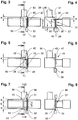
- Fig. 10 shows the basic arrangement of components of an ultrasonic welding apparatus 10, which includes a converter 12, a booster 14 and a sonotrode 16.
- the sonotrode 16 or one of these associated counter electrode 21 limit, as in particular in Fig.1 is shown, in a first axis direction (z-axis), a compression chamber 18 which is adjustable in height and width in order to adjust the cross section of the compression chamber 18 to the number or cross section of the conductors to be welded together.
- the converter 12 is connected via a line 11 to a generator 13, which in turn is connected via a line 15 to a computer 17 to input welding parameters or the cross-sectional geometry of the conductors to be welded together.
- the power output of the generator 13 can then be determined in order to retrieve the required welding parameters by means of a program stored in the computer 17 and to generate ultrasonic vibrations correspondingly by means of the converter 12, which transmit via the booster 14 to the sonotrode 16 or its working surface 19 ( FIG. Fig.1 ) .
- the compression chamber 18 is in the first axial direction (z-axis) on two opposite sides by a working surface 19 of the ultrasonic vibrations transmitting sonotrode 16 and a Counter-surface 20 limited in a second axis direction (y-axis) movable counter electrode 21.
- the in Fig. 1 is represented by the y-axis
- the compression space 18 is bounded on two opposite sides by a boundary surface 22 of a movable in the y-axis direction slider element 23 and a boundary surface 24 of the same as the counter electrode 21 movable in the z-axis direction limiting element 25.
- FIG. 1 illustrated embodiment of the compression chamber 18 are two stacked arrangement one above the other arranged connecting portions 26, 27 of each other by means of an ultrasonic welding connection to be connected conductors 28, 29 on the working surface 19 of the sonotrode 16, said Fig. 1 the connecting regions 26, 27 immediately after insertion into the open compression chamber 18 shows.
- Fig. 2 shows the compression chamber 18 in the closed configuration in which the compaction space 18 delimiting components, so the sonotrode 16, the counter electrode 21, the slider element 23 and the limiting element 25, are moved against each other so that the now reduced in its volume compression space 18 a Form 40 forms when an impact on the connection areas 26, 27 of the conductors 28, 29 with mechanical vibrations of the sonotrode 16 in a friction welding a compression and connection of the connecting portions 26, 27 together to form a welding node allows.
- Fig. 1 shown stacking arrangement of the connecting portions 26, 27 of the conductors 28, 29 may, as in the 3 and 4 represented by an equidirectional alignment of the conductors 28, 29 take place, wherein the conductors 28, 29 with their freed from an insulating sheath 30 blank areas 33, 34 are inserted so far into the compression space 18 in the x-axis direction that by the distance a , with the end cross-sections 31, 32 of the conductors 28, 29 are removed from a side edge 43 of the working surface 19, a predetermined length l 1 of the connecting portions 26, 27 results.
- the length l of the blank regions 33, 34 is selected such that a likewise generally predetermined distance l 2 remains between the connecting region 26, 27 and an axial envelope end face 35, 36.
- the compression chamber 18 is provided with an in Fig. 1 Marking device 37 shown schematically having a radiation emission device 38. Like a synopsis of Fig. 1 and 2 illustrates, is emitted from the radiation emitter 38, which is in the case of the present embodiment, a laser radiation source, along a beam path 39 laser radiation emitted at the in Fig. 1 illustrated embodiment of the marking device 37 is deflected via a beam deflection device 41 in the z-axis direction and in a reflection point, which forms a position mark 42, incident on the working surface 19 of the sonotrode 16.
- the beam path 39 is by means of the beam deflection device 41 or by means of the Strahlumlenk issued 41 comprehensive Strahlungsleitleaned, such as a fiber optic cable, not shown here, to adjust a defined beam path 39 so adjustable that the position mark 42 is formed at the location on the working surface 19 of the sonotrode 16, the desired distance a between the side edge 43 and the end sections 31, 32nd the conductor 28, 29 defined.
- the marking device 37 is basically not only suitable for use in the manufacture of a device in the 3 and 4 Endsch spakotens shown 44, but also for producing a defined in its geometry terminal welding node 45, as in the FIGS. 5 and 6 shown, and a passage welding node 46, which in the FIGS. 7 and 8 is shown.
- terminal welding node 45 is carried out in the same manner as above with reference to the 3 and 4
- a terminal 47 is arranged on the blank portion 33 of the conductor 28 in stacked arrangement, which is provided with a, here formed by a notch, marking 48, which in Cover can be brought with the position mark 42.
- suitable markings can also be through stamping lines or other visually recognizable Be formed features.
- the marking device 37 makes it possible to produce a welding node defined in its geometry, which has the end cross-section 31 of the connecting region 26 at a defined distance a from a flush with the side edge 43 the work surface 19 of the sonotrode 16 arranged counter surface 49 of the terminal, so that a compression of the end section 31 against the counter surface 49 during the vibration exposure of the connecting portion 26 is excluded by the sonotrode 16.
- the use of a marking device 50 for forming the passage kneading node 46 shows Figure 9 in an isometric view.
- the marking device 50 has a Strahlungsleit prepared 51 with two beam conductors 52, 53, each defining a beam path 54, 55, each beam path 54, 55 allows the formation of a position mark 56, 57 on the working surface 19 of the sonotrode 16.
- the marking device 50 has two radiation emission devices 58, which respectively generate the beam path 54, 55.
- the beam paths 54, 55 are each deflected by a beam deflection device 59 on the z-axis.
- the radiation emission devices 58 are located above the counter electrode 21 of the compression space 18 and opposite the slide element 23, such that the radiation emission devices 58 in FIG Horizontal direction (y-axis) generated beam paths 54, 55 are deflected by means of the beam deflector 59 in the vertical direction (z-axis) to impinge in each case at a reflection point on the working surface 19 of the sonotrode 16 for forming the position marks 56 and 57.
Landscapes
- Engineering & Computer Science (AREA)
- Mechanical Engineering (AREA)
- Manufacturing & Machinery (AREA)
- Manufacturing Of Electrical Connectors (AREA)
- Pressure Welding/Diffusion-Bonding (AREA)
- Laser Beam Processing (AREA)
Priority Applications (2)
| Application Number | Priority Date | Filing Date | Title |
|---|---|---|---|
| PL14803062T PL3069418T3 (pl) | 2013-11-11 | 2014-11-06 | Urządzenie do zgrzewania przewodów elektrycznych |
| RS20181091A RS57828B1 (sr) | 2013-11-11 | 2014-11-06 | Uređaj za zavarivanje električnih provodnika |
Applications Claiming Priority (2)
| Application Number | Priority Date | Filing Date | Title |
|---|---|---|---|
| DE201310222939 DE102013222939B3 (de) | 2013-11-11 | 2013-11-11 | Vorrichtung zum Verschweißen von elektrischen Leitern |
| PCT/EP2014/073939 WO2015067698A1 (de) | 2013-11-11 | 2014-11-06 | VORRICHTUNG ZUM VERSCHWEIßEN VON ELEKTRISCHEN LEITERN |
Publications (2)
| Publication Number | Publication Date |
|---|---|
| EP3069418A1 EP3069418A1 (de) | 2016-09-21 |
| EP3069418B1 true EP3069418B1 (de) | 2018-07-18 |
Family
ID=51987125
Family Applications (1)
| Application Number | Title | Priority Date | Filing Date |
|---|---|---|---|
| EP14803062.0A Active EP3069418B1 (de) | 2013-11-11 | 2014-11-06 | Vorrichtung zum verschweissen von elektrischen leitern |
Country Status (9)
| Country | Link |
|---|---|
| US (1) | US20160294140A1 (pl) |
| EP (1) | EP3069418B1 (pl) |
| CN (1) | CN105900297B (pl) |
| DE (1) | DE102013222939B3 (pl) |
| MX (1) | MX359803B (pl) |
| PL (1) | PL3069418T3 (pl) |
| RS (1) | RS57828B1 (pl) |
| TR (1) | TR201814956T4 (pl) |
| WO (1) | WO2015067698A1 (pl) |
Families Citing this family (10)
| Publication number | Priority date | Publication date | Assignee | Title |
|---|---|---|---|---|
| DE102013222938B3 (de) * | 2013-11-11 | 2015-04-30 | Schunk Sonosystems Gmbh | Vorrichtung zum Verschweißen von elektrischen Leitern |
| DE102016214227B3 (de) * | 2016-08-02 | 2017-12-07 | Schunk Sonosystems Gmbh | Vorrichtung und Verfahren zur Herstellung einer geprüften Schweißverbindung |
| MA49132B1 (fr) * | 2017-05-15 | 2021-09-30 | Schunk Sonosystems Gmbh | Dispositif de soudage de conducteurs électriques en forme de barres |
| DE102017119809A1 (de) * | 2017-08-29 | 2019-02-28 | Schunk Sonosystems Gmbh | Verfahren zum Schweißen von elektrischen Leitern sowie Ultraschallmetallschweißvorrichtung |
| JP6655056B2 (ja) * | 2017-11-28 | 2020-02-26 | 矢崎総業株式会社 | 電線の導体の超音波接合方法、端子付き電線の製造方法および電線 |
| PL3906133T3 (pl) * | 2019-11-05 | 2022-06-20 | Schunk Sonosystems Gmbh | Urządzenie do zgrzewania ultradźwiękowego z wykrywaniem pozycjonowania elementów łączonych |
| RS64370B1 (sr) * | 2019-11-05 | 2023-08-31 | Schunk Sonosystems Gmbh | Uređaj za ultrazvučno zavarivanje sa prihvatnikom u obliku slova v delova za spajanje |
| MX2022005429A (es) | 2019-11-05 | 2022-06-16 | Schunk Sonosystems Gmbh | Dispositivo de soldadura ultrasonica con elemento de tope desplazable. |
| DE102020113672B4 (de) | 2020-05-20 | 2022-03-03 | Lisa Dräxlmaier GmbH | Verfahren und vorrichtung zum verschweissen von zumindest drei kabeln mit je zwei aus mantelenden der kabel herausragenden adern |
| EP4697507A1 (de) * | 2024-08-16 | 2026-02-18 | Telsonic Holding AG | Verfahren zum verbinden von elektrischen leitern, insbesondere mit ultraschallschwingungen, verbindungs-, insbesondere ultraschallverbindungsvorrichtung, verfahren zum verbinden von elektrischen leitern mit der verbindungsvorrichtung sowie sonotrode und verfahren mit einer sonotrode zum verbinden von elektrischen leitern |
Family Cites Families (7)
| Publication number | Priority date | Publication date | Assignee | Title |
|---|---|---|---|---|
| US4472056A (en) * | 1980-07-23 | 1984-09-18 | Hitachi, Ltd. | Shape detecting apparatus |
| US4867370A (en) * | 1987-04-09 | 1989-09-19 | American Technology, Inc. | Apparatus and method for ultrasonic welding of wires |
| DE4116316A1 (de) * | 1991-05-15 | 1992-11-19 | Siemens Ag | Verfahren zum anbringen eines kontaktelementes am ende eines isolierten leiters |
| AU2217999A (en) * | 1998-01-08 | 1999-07-26 | Paul Akers | Laser levelling system, apparatus and method for building construction |
| DE102004033575B3 (de) * | 2004-07-09 | 2006-04-13 | Schunk Ultraschalltechnik Gmbh | Anordnung zum Verschweißen von Werkstücken |
| JP4888127B2 (ja) * | 2007-01-17 | 2012-02-29 | コニカミノルタセンシング株式会社 | 三次元測定装置及び携帯型計測器 |
| US20140002608A1 (en) * | 2011-12-28 | 2014-01-02 | Faro Technologies, Inc. | Line scanner using a low coherence light source |
-
2013
- 2013-11-11 DE DE201310222939 patent/DE102013222939B3/de active Active
-
2014
- 2014-11-06 RS RS20181091A patent/RS57828B1/sr unknown
- 2014-11-06 US US15/035,374 patent/US20160294140A1/en not_active Abandoned
- 2014-11-06 EP EP14803062.0A patent/EP3069418B1/de active Active
- 2014-11-06 TR TR2018/14956T patent/TR201814956T4/tr unknown
- 2014-11-06 PL PL14803062T patent/PL3069418T3/pl unknown
- 2014-11-06 MX MX2016005632A patent/MX359803B/es active IP Right Grant
- 2014-11-06 WO PCT/EP2014/073939 patent/WO2015067698A1/de not_active Ceased
- 2014-11-06 CN CN201480061610.0A patent/CN105900297B/zh active Active
Non-Patent Citations (1)
| Title |
|---|
| None * |
Also Published As
| Publication number | Publication date |
|---|---|
| DE102013222939B3 (de) | 2015-04-30 |
| MX359803B (es) | 2018-10-09 |
| WO2015067698A1 (de) | 2015-05-14 |
| RS57828B1 (sr) | 2018-12-31 |
| MX2016005632A (es) | 2016-10-26 |
| TR201814956T4 (tr) | 2018-11-21 |
| EP3069418A1 (de) | 2016-09-21 |
| US20160294140A1 (en) | 2016-10-06 |
| CN105900297A (zh) | 2016-08-24 |
| CN105900297B (zh) | 2018-10-12 |
| PL3069418T3 (pl) | 2019-01-31 |
Similar Documents
| Publication | Publication Date | Title |
|---|---|---|
| EP3069418B1 (de) | Vorrichtung zum verschweissen von elektrischen leitern | |
| EP2609655B1 (de) | Verfahren und vorrichtung zum verbinden eines elektrischen leiters mit einem elektrischen kontaktteil | |
| DE102013222938B3 (de) | Vorrichtung zum Verschweißen von elektrischen Leitern | |
| EP3017509B1 (de) | Verfahren zum verbinden eines elektrischen leiters mit einem elektrischen kontaktteil | |
| EP2003477A1 (de) | Elektro-optische Hybrid-Steckverbindung zur Übertragung von hohen optischen Leistungen und elektrischen Signalen | |
| EP3921885B1 (de) | Herstellen eines niedervoltpfades eines zellkontaktiersystems | |
| EP3627636B1 (de) | Elektrische steckverbindung, baugruppenverbindung und leiterplattenanordnung | |
| WO2020098868A1 (de) | Laserschneidevorrichtung für geschirmte leitungen und verfahren zum laserschneiden von geschirmten leitungen mit einer solchen laserschneidevorrichtung | |
| EP2590003B1 (de) | Vorrichtung zum Einstellen eines Strahlprofils, Laserbearbeitungsmaschine und Verfahren zur Herstellung der Vorrichtung | |
| EP3965973B1 (de) | Umformmaschine und herstellverfahren für biegeteile aus isoliertem länglichem material mit abisolierten enden | |
| DE102012007846B4 (de) | Crimpvorrichtung zum Verbinden eines elektrischen Leiters mit einem elektrischen Kontaktteil, das verformbare Schenkel aufweist | |
| EP1972033A2 (de) | Kontaktzelle zur aufnahme eines kabelendes mittels schneidklemmtechnik und verfahren zu deren herstellung | |
| DE102009027967A1 (de) | Verfahren und Vorrichtung zur Überwachung der Abisolierung von Leitungsenden | |
| DE68905764T2 (de) | Verfahren zur Herstellung eines Faserkopplers. | |
| DE102021108215B3 (de) | Verfahren und Vorrichtung zum Bearbeiten eines Kabels | |
| EP4492104A1 (de) | Multilichtwellenleiterstecker sowie lichtwellenleiterverbinder mit einem solchen | |
| EP4188632B1 (de) | Verfahren zum mehrstufigen schweissen von knoten mittels einer ultraschallschweisseinrichtung | |
| DE102020104417B4 (de) | Anschlussklemme | |
| EP3373055A1 (de) | Elektrooptische schaltung mit einer optischen übertragungsstrecke, elektrooptische baugruppe zum einbau in eine solche elektrooptische schaltung und verfahren zum erzeugen einer optischen schnittstelle einer elektrooptischen schaltung | |
| DE19931944A1 (de) | Umlenkende Auskopplung in einer Leiterplatte eingebetteter Lichtleiter | |
| EP3133704A1 (de) | Verfahren zum verbinden einer elektrischen leitung mit einem kontaktelement | |
| EP4595171B1 (de) | Verfahren zum verschweissen von leitungen zu einer y- oder x-verbindung mittels ultraschall | |
| DE10120694A1 (de) | Koppler für optische Signale und Verfahren zum Setzen mechanischer Führungselemente von Kopplern | |
| DE19952420C2 (de) | Verfahren und Vorrichtung zur Durchgängigkeitsprüfung für einen Lichtwellenleiter | |
| EP3646414B1 (de) | Verfahren zur herstellung einer bauelementanordnung mit drahtverbindung sowie bauelementanordnung mit drahtverbindung |
Legal Events
| Date | Code | Title | Description |
|---|---|---|---|
| PUAI | Public reference made under article 153(3) epc to a published international application that has entered the european phase |
Free format text: ORIGINAL CODE: 0009012 |
|
| 17P | Request for examination filed |
Effective date: 20160608 |
|
| AK | Designated contracting states |
Kind code of ref document: A1 Designated state(s): AL AT BE BG CH CY CZ DE DK EE ES FI FR GB GR HR HU IE IS IT LI LT LU LV MC MK MT NL NO PL PT RO RS SE SI SK SM TR |
|
| AX | Request for extension of the european patent |
Extension state: BA ME |
|
| RIN1 | Information on inventor provided before grant (corrected) |
Inventor name: DR. TRUBE, STEFAN Inventor name: STROH, DIETER Inventor name: KOC, SINAN Inventor name: WAGNER, PETER Inventor name: SCHMIDT, REINER |
|
| DAX | Request for extension of the european patent (deleted) | ||
| REG | Reference to a national code |
Ref country code: DE Ref legal event code: R079 Ref document number: 502014008902 Country of ref document: DE Free format text: PREVIOUS MAIN CLASS: H01R0043020000 Ipc: B23K0020020000 |
|
| GRAP | Despatch of communication of intention to grant a patent |
Free format text: ORIGINAL CODE: EPIDOSNIGR1 |
|
| STAA | Information on the status of an ep patent application or granted ep patent |
Free format text: STATUS: GRANT OF PATENT IS INTENDED |
|
| RIC1 | Information provided on ipc code assigned before grant |
Ipc: B23K 20/02 20060101AFI20180112BHEP Ipc: B23K 101/38 20060101ALI20180112BHEP Ipc: B23K 20/26 20060101ALI20180112BHEP Ipc: H01R 43/02 20060101ALI20180112BHEP Ipc: B23K 20/10 20060101ALI20180112BHEP |
|
| INTG | Intention to grant announced |
Effective date: 20180206 |
|
| GRAS | Grant fee paid |
Free format text: ORIGINAL CODE: EPIDOSNIGR3 |
|
| GRAA | (expected) grant |
Free format text: ORIGINAL CODE: 0009210 |
|
| STAA | Information on the status of an ep patent application or granted ep patent |
Free format text: STATUS: THE PATENT HAS BEEN GRANTED |
|
| RIN1 | Information on inventor provided before grant (corrected) |
Inventor name: DR. TRUBE, STEFAN Inventor name: SCHMIDT, REINER Inventor name: KOC, SINAN Inventor name: WAGNER, PETER Inventor name: STROH, DIETER |
|
| AK | Designated contracting states |
Kind code of ref document: B1 Designated state(s): AL AT BE BG CH CY CZ DE DK EE ES FI FR GB GR HR HU IE IS IT LI LT LU LV MC MK MT NL NO PL PT RO RS SE SI SK SM TR |
|
| REG | Reference to a national code |
Ref country code: GB Ref legal event code: FG4D Free format text: NOT ENGLISH |
|
| REG | Reference to a national code |
Ref country code: CH Ref legal event code: EP |
|
| REG | Reference to a national code |
Ref country code: IE Ref legal event code: FG4D Free format text: LANGUAGE OF EP DOCUMENT: GERMAN |
|
| REG | Reference to a national code |
Ref country code: AT Ref legal event code: REF Ref document number: 1018832 Country of ref document: AT Kind code of ref document: T Effective date: 20180815 |
|
| REG | Reference to a national code |
Ref country code: DE Ref legal event code: R096 Ref document number: 502014008902 Country of ref document: DE |
|
| REG | Reference to a national code |
Ref country code: RO Ref legal event code: EPE |
|
| REG | Reference to a national code |
Ref country code: CH Ref legal event code: NV Representative=s name: BODENSEEPATENT PATENTANWAELTE BEHRMANN WAGNER , CH |
|
| REG | Reference to a national code |
Ref country code: NL Ref legal event code: MP Effective date: 20180718 |
|
| REG | Reference to a national code |
Ref country code: LT Ref legal event code: MG4D |
|
| PG25 | Lapsed in a contracting state [announced via postgrant information from national office to epo] |
Ref country code: NL Free format text: LAPSE BECAUSE OF FAILURE TO SUBMIT A TRANSLATION OF THE DESCRIPTION OR TO PAY THE FEE WITHIN THE PRESCRIBED TIME-LIMIT Effective date: 20180718 |
|
| PG25 | Lapsed in a contracting state [announced via postgrant information from national office to epo] |
Ref country code: FI Free format text: LAPSE BECAUSE OF FAILURE TO SUBMIT A TRANSLATION OF THE DESCRIPTION OR TO PAY THE FEE WITHIN THE PRESCRIBED TIME-LIMIT Effective date: 20180718 Ref country code: IS Free format text: LAPSE BECAUSE OF FAILURE TO SUBMIT A TRANSLATION OF THE DESCRIPTION OR TO PAY THE FEE WITHIN THE PRESCRIBED TIME-LIMIT Effective date: 20181118 Ref country code: GR Free format text: LAPSE BECAUSE OF FAILURE TO SUBMIT A TRANSLATION OF THE DESCRIPTION OR TO PAY THE FEE WITHIN THE PRESCRIBED TIME-LIMIT Effective date: 20181019 Ref country code: NO Free format text: LAPSE BECAUSE OF FAILURE TO SUBMIT A TRANSLATION OF THE DESCRIPTION OR TO PAY THE FEE WITHIN THE PRESCRIBED TIME-LIMIT Effective date: 20181018 Ref country code: SE Free format text: LAPSE BECAUSE OF FAILURE TO SUBMIT A TRANSLATION OF THE DESCRIPTION OR TO PAY THE FEE WITHIN THE PRESCRIBED TIME-LIMIT Effective date: 20180718 Ref country code: LT Free format text: LAPSE BECAUSE OF FAILURE TO SUBMIT A TRANSLATION OF THE DESCRIPTION OR TO PAY THE FEE WITHIN THE PRESCRIBED TIME-LIMIT Effective date: 20180718 |
|
| PG25 | Lapsed in a contracting state [announced via postgrant information from national office to epo] |
Ref country code: HR Free format text: LAPSE BECAUSE OF FAILURE TO SUBMIT A TRANSLATION OF THE DESCRIPTION OR TO PAY THE FEE WITHIN THE PRESCRIBED TIME-LIMIT Effective date: 20180718 Ref country code: LV Free format text: LAPSE BECAUSE OF FAILURE TO SUBMIT A TRANSLATION OF THE DESCRIPTION OR TO PAY THE FEE WITHIN THE PRESCRIBED TIME-LIMIT Effective date: 20180718 Ref country code: AL Free format text: LAPSE BECAUSE OF FAILURE TO SUBMIT A TRANSLATION OF THE DESCRIPTION OR TO PAY THE FEE WITHIN THE PRESCRIBED TIME-LIMIT Effective date: 20180718 |
|
| REG | Reference to a national code |
Ref country code: SK Ref legal event code: T3 Ref document number: E 29133 Country of ref document: SK |
|
| REG | Reference to a national code |
Ref country code: DE Ref legal event code: R097 Ref document number: 502014008902 Country of ref document: DE |
|
| PG25 | Lapsed in a contracting state [announced via postgrant information from national office to epo] |
Ref country code: ES Free format text: LAPSE BECAUSE OF FAILURE TO SUBMIT A TRANSLATION OF THE DESCRIPTION OR TO PAY THE FEE WITHIN THE PRESCRIBED TIME-LIMIT Effective date: 20180718 Ref country code: EE Free format text: LAPSE BECAUSE OF FAILURE TO SUBMIT A TRANSLATION OF THE DESCRIPTION OR TO PAY THE FEE WITHIN THE PRESCRIBED TIME-LIMIT Effective date: 20180718 |
|
| PLBE | No opposition filed within time limit |
Free format text: ORIGINAL CODE: 0009261 |
|
| STAA | Information on the status of an ep patent application or granted ep patent |
Free format text: STATUS: NO OPPOSITION FILED WITHIN TIME LIMIT |
|
| PG25 | Lapsed in a contracting state [announced via postgrant information from national office to epo] |
Ref country code: SM Free format text: LAPSE BECAUSE OF FAILURE TO SUBMIT A TRANSLATION OF THE DESCRIPTION OR TO PAY THE FEE WITHIN THE PRESCRIBED TIME-LIMIT Effective date: 20180718 Ref country code: DK Free format text: LAPSE BECAUSE OF FAILURE TO SUBMIT A TRANSLATION OF THE DESCRIPTION OR TO PAY THE FEE WITHIN THE PRESCRIBED TIME-LIMIT Effective date: 20180718 |
|
| 26N | No opposition filed |
Effective date: 20190423 |
|
| GBPC | Gb: european patent ceased through non-payment of renewal fee |
Effective date: 20181106 |
|
| PG25 | Lapsed in a contracting state [announced via postgrant information from national office to epo] |
Ref country code: MC Free format text: LAPSE BECAUSE OF FAILURE TO SUBMIT A TRANSLATION OF THE DESCRIPTION OR TO PAY THE FEE WITHIN THE PRESCRIBED TIME-LIMIT Effective date: 20180718 Ref country code: LU Free format text: LAPSE BECAUSE OF NON-PAYMENT OF DUE FEES Effective date: 20181106 |
|
| REG | Reference to a national code |
Ref country code: BE Ref legal event code: MM Effective date: 20181130 |
|
| REG | Reference to a national code |
Ref country code: IE Ref legal event code: MM4A |
|
| PG25 | Lapsed in a contracting state [announced via postgrant information from national office to epo] |
Ref country code: SI Free format text: LAPSE BECAUSE OF FAILURE TO SUBMIT A TRANSLATION OF THE DESCRIPTION OR TO PAY THE FEE WITHIN THE PRESCRIBED TIME-LIMIT Effective date: 20180718 |
|
| PG25 | Lapsed in a contracting state [announced via postgrant information from national office to epo] |
Ref country code: IE Free format text: LAPSE BECAUSE OF NON-PAYMENT OF DUE FEES Effective date: 20181106 Ref country code: FR Free format text: LAPSE BECAUSE OF NON-PAYMENT OF DUE FEES Effective date: 20181130 |
|
| PG25 | Lapsed in a contracting state [announced via postgrant information from national office to epo] |
Ref country code: BE Free format text: LAPSE BECAUSE OF NON-PAYMENT OF DUE FEES Effective date: 20181130 |
|
| PG25 | Lapsed in a contracting state [announced via postgrant information from national office to epo] |
Ref country code: GB Free format text: LAPSE BECAUSE OF NON-PAYMENT OF DUE FEES Effective date: 20181106 |
|
| PG25 | Lapsed in a contracting state [announced via postgrant information from national office to epo] |
Ref country code: MT Free format text: LAPSE BECAUSE OF FAILURE TO SUBMIT A TRANSLATION OF THE DESCRIPTION OR TO PAY THE FEE WITHIN THE PRESCRIBED TIME-LIMIT Effective date: 20180718 |
|
| PG25 | Lapsed in a contracting state [announced via postgrant information from national office to epo] |
Ref country code: PT Free format text: LAPSE BECAUSE OF FAILURE TO SUBMIT A TRANSLATION OF THE DESCRIPTION OR TO PAY THE FEE WITHIN THE PRESCRIBED TIME-LIMIT Effective date: 20180718 |
|
| PG25 | Lapsed in a contracting state [announced via postgrant information from national office to epo] |
Ref country code: CY Free format text: LAPSE BECAUSE OF FAILURE TO SUBMIT A TRANSLATION OF THE DESCRIPTION OR TO PAY THE FEE WITHIN THE PRESCRIBED TIME-LIMIT Effective date: 20180718 Ref country code: MK Free format text: LAPSE BECAUSE OF NON-PAYMENT OF DUE FEES Effective date: 20180718 |
|
| REG | Reference to a national code |
Ref country code: AT Ref legal event code: MM01 Ref document number: 1018832 Country of ref document: AT Kind code of ref document: T Effective date: 20191106 |
|
| PG25 | Lapsed in a contracting state [announced via postgrant information from national office to epo] |
Ref country code: AT Free format text: LAPSE BECAUSE OF NON-PAYMENT OF DUE FEES Effective date: 20191106 |
|
| REG | Reference to a national code |
Ref country code: CH Ref legal event code: PFA Owner name: SCHUNK SONOSYSTEMS GMBH, DE Free format text: FORMER OWNER: SCHUNK SONOSYSTEMS GMBH, DE |
|
| P01 | Opt-out of the competence of the unified patent court (upc) registered |
Effective date: 20230524 |
|
| REG | Reference to a national code |
Ref country code: CH Ref legal event code: U11 Free format text: ST27 STATUS EVENT CODE: U-0-0-U10-U11 (AS PROVIDED BY THE NATIONAL OFFICE) Effective date: 20251201 |
|
| PGFP | Annual fee paid to national office [announced via postgrant information from national office to epo] |
Ref country code: HU Payment date: 20251107 Year of fee payment: 12 |
|
| PGFP | Annual fee paid to national office [announced via postgrant information from national office to epo] |
Ref country code: DE Payment date: 20251126 Year of fee payment: 12 |
|
| PGFP | Annual fee paid to national office [announced via postgrant information from national office to epo] |
Ref country code: IT Payment date: 20251121 Year of fee payment: 12 |
|
| PGFP | Annual fee paid to national office [announced via postgrant information from national office to epo] |
Ref country code: TR Payment date: 20251023 Year of fee payment: 12 |
|
| PGFP | Annual fee paid to national office [announced via postgrant information from national office to epo] |
Ref country code: CH Payment date: 20251201 Year of fee payment: 12 |
|
| PGFP | Annual fee paid to national office [announced via postgrant information from national office to epo] |
Ref country code: CZ Payment date: 20251103 Year of fee payment: 12 |
|
| PGFP | Annual fee paid to national office [announced via postgrant information from national office to epo] |
Ref country code: BG Payment date: 20251124 Year of fee payment: 12 Ref country code: PL Payment date: 20251031 Year of fee payment: 12 |
|
| PGFP | Annual fee paid to national office [announced via postgrant information from national office to epo] |
Ref country code: RO Payment date: 20251030 Year of fee payment: 12 Ref country code: SK Payment date: 20251027 Year of fee payment: 12 |
|
| PGFP | Annual fee paid to national office [announced via postgrant information from national office to epo] |
Ref country code: RS Payment date: 20251027 Year of fee payment: 12 |