EP3067953B1 - Anzeigevorrichtung und herstellungsverfahren dafür - Google Patents
Anzeigevorrichtung und herstellungsverfahren dafür Download PDFInfo
- Publication number
- EP3067953B1 EP3067953B1 EP15196452.5A EP15196452A EP3067953B1 EP 3067953 B1 EP3067953 B1 EP 3067953B1 EP 15196452 A EP15196452 A EP 15196452A EP 3067953 B1 EP3067953 B1 EP 3067953B1
- Authority
- EP
- European Patent Office
- Prior art keywords
- spacer
- inclination
- display device
- layer
- substrate
- Prior art date
- Legal status (The legal status is an assumption and is not a legal conclusion. Google has not performed a legal analysis and makes no representation as to the accuracy of the status listed.)
- Active
Links
Images








Classifications
-
- H—ELECTRICITY
- H10—SEMICONDUCTOR DEVICES; ELECTRIC SOLID-STATE DEVICES NOT OTHERWISE PROVIDED FOR
- H10K—ORGANIC ELECTRIC SOLID-STATE DEVICES
- H10K59/00—Integrated devices, or assemblies of multiple devices, comprising at least one organic light-emitting element covered by group H10K50/00
- H10K59/10—OLED displays
- H10K59/12—Active-matrix OLED [AMOLED] displays
- H10K59/122—Pixel-defining structures or layers, e.g. banks
-
- H—ELECTRICITY
- H10—SEMICONDUCTOR DEVICES; ELECTRIC SOLID-STATE DEVICES NOT OTHERWISE PROVIDED FOR
- H10K—ORGANIC ELECTRIC SOLID-STATE DEVICES
- H10K50/00—Organic light-emitting devices
- H10K50/80—Constructional details
- H10K50/84—Passivation; Containers; Encapsulations
-
- H—ELECTRICITY
- H10—SEMICONDUCTOR DEVICES; ELECTRIC SOLID-STATE DEVICES NOT OTHERWISE PROVIDED FOR
- H10K—ORGANIC ELECTRIC SOLID-STATE DEVICES
- H10K50/00—Organic light-emitting devices
- H10K50/80—Constructional details
- H10K50/84—Passivation; Containers; Encapsulations
- H10K50/842—Containers
- H10K50/8428—Vertical spacers, e.g. arranged between the sealing arrangement and the OLED
-
- H—ELECTRICITY
- H10—SEMICONDUCTOR DEVICES; ELECTRIC SOLID-STATE DEVICES NOT OTHERWISE PROVIDED FOR
- H10K—ORGANIC ELECTRIC SOLID-STATE DEVICES
- H10K59/00—Integrated devices, or assemblies of multiple devices, comprising at least one organic light-emitting element covered by group H10K50/00
- H10K59/10—OLED displays
- H10K59/12—Active-matrix OLED [AMOLED] displays
- H10K59/121—Active-matrix OLED [AMOLED] displays characterised by the geometry or disposition of pixel elements
- H10K59/1213—Active-matrix OLED [AMOLED] displays characterised by the geometry or disposition of pixel elements the pixel elements being TFTs
-
- H—ELECTRICITY
- H10—SEMICONDUCTOR DEVICES; ELECTRIC SOLID-STATE DEVICES NOT OTHERWISE PROVIDED FOR
- H10K—ORGANIC ELECTRIC SOLID-STATE DEVICES
- H10K59/00—Integrated devices, or assemblies of multiple devices, comprising at least one organic light-emitting element covered by group H10K50/00
- H10K59/10—OLED displays
- H10K59/12—Active-matrix OLED [AMOLED] displays
- H10K59/123—Connection of the pixel electrodes to the thin film transistors [TFT]
-
- H—ELECTRICITY
- H10—SEMICONDUCTOR DEVICES; ELECTRIC SOLID-STATE DEVICES NOT OTHERWISE PROVIDED FOR
- H10K—ORGANIC ELECTRIC SOLID-STATE DEVICES
- H10K59/00—Integrated devices, or assemblies of multiple devices, comprising at least one organic light-emitting element covered by group H10K50/00
- H10K59/10—OLED displays
- H10K59/12—Active-matrix OLED [AMOLED] displays
- H10K59/124—Insulating layers formed between TFT elements and OLED elements
-
- H—ELECTRICITY
- H10—SEMICONDUCTOR DEVICES; ELECTRIC SOLID-STATE DEVICES NOT OTHERWISE PROVIDED FOR
- H10K—ORGANIC ELECTRIC SOLID-STATE DEVICES
- H10K59/00—Integrated devices, or assemblies of multiple devices, comprising at least one organic light-emitting element covered by group H10K50/00
- H10K59/10—OLED displays
- H10K59/12—Active-matrix OLED [AMOLED] displays
- H10K59/131—Interconnections, e.g. wiring lines or terminals
-
- H—ELECTRICITY
- H10—SEMICONDUCTOR DEVICES; ELECTRIC SOLID-STATE DEVICES NOT OTHERWISE PROVIDED FOR
- H10K—ORGANIC ELECTRIC SOLID-STATE DEVICES
- H10K59/00—Integrated devices, or assemblies of multiple devices, comprising at least one organic light-emitting element covered by group H10K50/00
- H10K59/80—Constructional details
- H10K59/87—Passivation; Containers; Encapsulations
- H10K59/871—Self-supporting sealing arrangements
- H10K59/8723—Vertical spacers, e.g. arranged between the sealing arrangement and the OLED
-
- H—ELECTRICITY
- H10—SEMICONDUCTOR DEVICES; ELECTRIC SOLID-STATE DEVICES NOT OTHERWISE PROVIDED FOR
- H10K—ORGANIC ELECTRIC SOLID-STATE DEVICES
- H10K59/00—Integrated devices, or assemblies of multiple devices, comprising at least one organic light-emitting element covered by group H10K50/00
- H10K59/10—OLED displays
- H10K59/12—Active-matrix OLED [AMOLED] displays
- H10K59/1201—Manufacture or treatment
-
- H—ELECTRICITY
- H10—SEMICONDUCTOR DEVICES; ELECTRIC SOLID-STATE DEVICES NOT OTHERWISE PROVIDED FOR
- H10K—ORGANIC ELECTRIC SOLID-STATE DEVICES
- H10K59/00—Integrated devices, or assemblies of multiple devices, comprising at least one organic light-emitting element covered by group H10K50/00
- H10K59/80—Constructional details
- H10K59/88—Dummy elements, i.e. elements having non-functional features
Definitions
- the invention relates to a display device and a manufacturing method thereof.
- a display device such as for example a liquid crystal display (LCD), an organic light emitting diode (OLED) display, and an electrophoretic display, includes a field generating electrode and an electro-optical active layer.
- the LCD device includes a liquid crystal layer as the electro-optical active layer.
- the field generating electrode is connected to a switching element such as a thin film transistor to receive a data signal, and the electro-optical active layer converts the data signal into an optical signal to display an image.
- the organic light emitting diode (OLED) display as a self-light emitting type does not require a separate light source, it is advantageous in terms of power consumption, and a response speed, a viewing angle, and a contrast ratio thereof are excellent.
- the organic light emitting diode (OLED) display includes a plurality of pixels such as red pixels, blue pixels, green pixels, and white pixels, and may express full colors by combining the pixels.
- Each pixel includes an organic light emitting element, and a plurality of thin film transistors for driving the organic light emitting element.
- the light emitting element of the organic light emitting diode (OLED) display includes a pixel electrode, an opposing electrode, and a light emitting layer positioned between the two electrodes.
- One of the pixel electrode and the opposing electrode is referred to as an anode, and the other electrode a cathode.
- An electron injected from the cathode and a hole injected from the anode are coupled with each other in the light emitting layer to form an exciton, and the exciton emits light while discharging energy.
- the opposing electrode is formed throughout a plurality of pixels to transfer a predetermined common voltage.
- sealing is performed so that an internal element is separated from the outside to prevent impurities such as moisture from penetrating.
- a sealing method in the case of the organic light emitting diode (OLED) display, may be generally, a method of laminating a layer including an organic polymer such as polyethylene terephtalate (PET) on a completed lower substrate, a method of forming a cover or a cap on an encapsulation substrate and sealing an edge of a cover lower substrate and the encapsulation substrate with a sealant, or the like.
- Display devices are known from US2015/0034921 A1 or KR2013/0137455 A .
- a display device according to the invention is defined in claim 1. Preferred embodiments are defined in the dependent claims. A method for manufacturing the display device of claim 1 is defined in claim 12.
- the impact wave When applying an impact to the inventive display device including the sealant, the impact wave is effectively dispersed such that the impact wave may be prevented from being transmitted to the sealant, thereby increasing the strength of the display device.
- Adhesion reliability of the encapsulation region may be increased without a failure of the electrode of the display device including the sealant.
- a display device having the narrow bezel while having high strength may be provided.
- a display device according to an embodiment of the invention will be described with reference to FIG. 1 to FIG. 8 .
- FIG. 1 is a layout view of a display device
- FIG. 2 is a cross-sectional view of one pixel of the display device
- FIG. 3 is a layout view of a peripheral area of a display device according to an embodiment
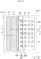
- FIG. 4 is an enlarged layout view of a region A, a region B, or a region C as a part of a peripheral area of the display device shown in FIG. 3
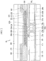
- FIG. 5 is a cross-sectional view of the display device of FIG. 4 taken along a line V-V
- FIG. 6 is a cross-sectional view of the display device of FIG. 4 taken along a line VI-VI.
- a display panel 1 of a display device includes a display area DA which is an area displaying an image, and a peripheral area PA therearound when viewed in a plan view.
- the display device 1 when viewed from a cross-sectional view, the display device 1 includes a lower substrate 110 and an encapsulation substrate 210 facing each other.
- the lower substrate 110 includes the display area DA and the peripheral area PA1 therearound, and the encapsulation substrate 210 includes the display area DA and the peripheral area PA2 therearound.
- the peripheral area PA2 of the encapsulation substrate 210 may be included in the peripheral area PA1 of the lower substrate 110.
- the peripheral area PA of the display device 1 includes the peripheral area PA1 of the lower substrate 110 and the peripheral area PA2 of the encapsulation substrate 210.
- edges of the encapsulation substrate 210 may include an upper side edge E1, a lower side edge E2 facing the upper side edge E1, and a right side edge E3 and a left side edge E4 connecting between the upper side edge E1 and the lower side edge E2.
- the upper side edge E1, the lower side edge E2, the right side edge E3, or the left side edge E4 may each substantially be a straight line, and at least one thereof may include a curved line portion.
- the display area DA includes a plurality of signal lines and a plurality of pixels PX connected to the signal lines.
- the plurality of pixels PX may be arranged substantially in a matrix form, however they are not limited thereto.
- the signal lines are provided on the lower substrate 110, and include a plurality of gate lines or scanning signal lines G1-Gn transferring scanning signals, and a plurality of data lines D1-Dm transferring data voltages.
- the gate lines G1-Gn extend substantially in a row direction and are almost parallel to each other, and the data lines D1-Dm extend substantially in a column direction and are almost parallel to each other.
- the pixel PX positioned in the display area DA may include at least one switching element Qd connected to at least one of gate lines G1-Gn, and at least one of data lines D1-Dm and data line 171, at least one pixel electrode 191 connected to the switching element Qd, and an opposing electrode 270.
- a light emitting layer is positioned between the pixel electrode 191 and the opposing electrode 270 to form a light emitting element.
- the switching element Qd may include at least one thin film transistor.
- the opposing electrode 270 may transmit a common voltage ELVSS.
- each pixel PX may display one of primary colors, and a desired color may be recognized by combining the primary colors.
- Primary colors may include three primary colors or four primary colors such as red, green, blue, and the like.
- Each pixel PX may further include a color filter positioned at a place corresponding to each pixel electrode and expressing one of the primary colors, and the light emitting layer may be a colored light emitting layer.
- the encapsulation substrate 210 may expose a part of the peripheral area PA1 of the lower substrate 110, and the exposed part is referred to as a pad part.
- at least one data driver 500 to drive the light-emitting device may be mounted in a type of at least one IC chip.
- the driver 500 may be mounted on a flexible printed circuit (FPC) film or a printing circuit board to be attached to the pad part in a type of a TCP (tape carrier package), or may be directly integrated with the lower substrate 110.
- FPC flexible printed circuit
- TCP tape carrier package
- ends extended from the signal lines such as the data lines D1-Dm of the display area DA may be positioned.
- the data driver 500 may be connected to the end of the data lines D1-Dm and transmitting a data signal to the data lines D1-Dm.
- a gate driver 400 to drive the light-emitting device may also be positioned in the peripheral area PA1 of the lower substrate 110 covered by the encapsulation substrate 210.
- the driver 400 may be mounted on the lower substrate 110 in the type of at least one IC chip, or may be mounted on the flexible printed circuit (FPC) film or the printing circuit board to be attached to the lower substrate 110 in the type of the TCP, or may be integrated with the lower substrate 110.
- the gate driver 400 may be connected to the gate lines G1-Gn and transmitting the gate signal to the gate lines G1-Gn.
- a buffer layer 111 may be positioned on the peripheral area PA1 and the display area DA of the lower substrate 110 including transparent glass or plastic.
- the buffer layer 111 may prevent impurities from penetrating, and a surface thereof may be flat.
- the buffer layer 111 may include a silicon nitride (SiNx), a silicon oxide (SiOx), a silicon oxynitride (SiOxNy), or the like.
- the buffer layer 111 may be omitted in some embodiments.
- At least one semiconductor layer is positioned on the buffer layer 111.
- the semiconductor layer includes a first semiconductor 154b positioned in the display area DA.
- the first semiconductor 154b may include a channel region 152b, and a source region 153b and a drain region 155b positioned at respective sides of the channel region 152b and formed to be doped.
- the semiconductor layer may further include at least one second semiconductor 150d (see FIG. 5 ) positioned in the peripheral area PA1 of the lower substrate 110.
- the second semiconductor 150d may include a channel region, and a source region and a drain region positioned at respective sides of the channel region and formed to be doped.
- the semiconductor layer may include amorphous silicon, polysilicon, or an oxide semiconductor.
- a gate insulating layer 140 including a silicon nitride (SiNx) or a silicon oxide (SiOx) is positioned on the semiconductor layer.
- a plurality of gate conductors are positioned on the gate insulating layer 140.
- the gate conductor includes a first control electrode 124b positioned in the display area DA.
- the first control electrode 124b may overlap a part of the first semiconductor 154b, particularly the channel region.
- the gate conductor may further include at least one second control electrode 120d (see FIG. 5 ) positioned in the peripheral areas PA1 and PA2.
- the second control electrode 120d may include a part overlapping the second semiconductor 150d, particularly the channel region of the second semiconductor 150d.
- the gate conductor may further include a thermal transmission layer 23 (see FIG. 5 ) positioned in the peripheral area PA1 and PA2.
- a first passivation layer 180a is positioned on the gate insulating layer 140 and the gate conductor.
- the first passivation layer 180a and the gate insulating layer 140 may include a contact hole 183b exposing the source region 153b of the first semiconductor 154b, and a contact hole 185b exposing the drain region 155b in the display area DA.
- the first passivation layer 180a and the gate insulating layer 140 may include contact holes (not shown) respectively exposing the source region and the drain region of the second semiconductor 154d in the peripheral areas PA1 and PA2.
- a plurality of data conductors are positioned on the first passivation layer 180a.
- the data conductors may include a plurality of data lines 171, a driving voltage line (not shown), and a plurality of first output electrodes 175b.
- the driving voltage line transmits a driving voltage ELVDD and may include a plurality of first input electrodes 173b extending toward a first control electrode 124b.
- the first output electrode 175b faces the first input electrode 173b on the first semiconductor 154b.
- the first input electrode 173b and the first output electrode 175b may be respectively connected to the source region 153b and the drain region 155b of the first semiconductor 154b through the contact holes 183b and 185b.
- the data conductor may further include a voltage transmission line 177 (see FIG. 5 ) positioned in the peripheral area PA1 and PA2.
- the voltage transmission line 177 transmits a common voltage ELVSS.
- the voltage transmission line 177 may include a main transmission part 177a and an end 177b connected thereto.
- the main transmission part 177a is formed along the edge of the display area DA and extends along the upper side edge E1, the right side edge E3, and the left side edge E4 of the encapsulation substrate 210.
- the end 177b is positioned to be close to the lower side edge E2 and may extend to the pad part of the lower substrate 110.
- the end 177b may include two parts positioned at respective ends of the main transmission part 177a and separated from each other near the lower side edge E2, but is not limited thereto.
- the data conductor may further include at least one second input/output electrode 170d (see FIG. 5 ) positioned in the peripheral area PA1 and PA2.
- the data conductor may further include a test signal line 17te (see FIG. 5 ) positioned in the peripheral areas PA1 and PA2.
- the test signal line 17te may be omitted in some embodiments.
- the first control electrode 124b, the first input electrode 173b, and the first output electrode 175b form a switching element Qd as a transistor along the first semiconductor 154b.
- the structure of the switching element Qd is not limited thereto and may be changed in various embodiments.
- the second control electrode 120d, the second input/output electrode 170d, and the second semiconductor 150d may together form at least one transistor 411.
- the transistor 411 may be included in the driver to drive the light-emitting device.
- This driver may be the gate driver outputting the gate signal to the gate line G1-Gn.
- a second passivation layer 180b including an inorganic insulating material and/or an organic insulating material is positioned on the data conductor.
- the second passivation layer 180b may have a substantially flat surface to increase emission efficiency of the organic light emitting element to be formed thereon.
- the second passivation layer 180b may have a contact hole 185c exposing the first output electrode 175b in the display area DA.
- the second passivation layer 180b exposes at least a portion of the voltage transmission line 177.
- the second passivation layer 180b includes an edge side surface 186 positioned in the peripheral area PA1, and the edge side surface 186 may include a bottom side positioned in the top surface of the voltage transmission line 177. Accordingly, the second passivation layer 180b may expose the voltage transmission line 177 in the peripheral area PA1.
- a pixel electrode layer is positioned on the second passivation layer 180b.
- the pixel electrode layer includes a pixel electrode 191 positioned in each pixel PX of the display area DA.
- the pixel electrode 191 is physically and electrically connected to the first output electrode 175b through the contact hole 185c of the second passivation layer 180b.
- the pixel electrode layer may further include a voltage transmission electrode 197 positioned in the peripheral area PA1 and PA2.
- the voltage transmission electrode 197 includes a part covering the edge side surface 186 of the second passivation layer 180b in the peripheral areas PA1 and PA2 and is physically and electrically connected to the voltage transmission line 177, thereby receiving the common voltage ELVSS.
- the voltage transmission electrode 197 may form a step on the portion covering the edge side surface 186 of the second passivation layer 180b.
- the voltage transmission electrode 197 may be formed along the display area DA, for example, may be formed of a closed line enclosing the display area DA, but it is not limited thereto.
- the voltage transmission electrode 197 may extend with a uniform width as shown, however it may have different widths depending on the position. When the voltage transmission electrode 197 has a non-uniform width, portions having different widths may be alternately disposed.
- the voltage transmission electrode 197 may include a plurality of holes 97.
- the plurality of holes 97 are formed on the second passivation layer 180b.
- the holes 97 may be arranged in a predetermined type such as a matrix shape as an example, or not.
- the holes 97 provide an outlet exhausting a gas generated in the second passivation layer 180b when heat is applied in a subsequent process, thereby preventing the voltage transmission electrode 197 from being lifted from the second passivation layer 180b by the gas.
- the pixel electrode layer may include a semi-transmissive conductive material or a reflective conductive material.
- the layers on the lower substrate 110 for example, the layers from the buffer layer 111 to the second passivation layer 180b, are referred to together as a transistor layer TFL.
- a pixel definition layer 360 is positioned on the second passivation layer 180b and the pixel electrode layer.
- the pixel definition layer 360 includes a spacer 360F having a higher top surface than the top surface of the main portion 360H with respect to a main portion 360H and the lower substrate 110.
- the spacer 360F is formed to be higher than the main portion 360H such that the top surface may contact the surface of the encapsulation substrate 210.
- the spacer 360F may uniformly maintain a separation distance between the encapsulation substrate 210 and the lower substrate 110.
- the main portion 360H of the pixel definition layer 360 positioned in the display area DA has a plurality of holes 365 defining a region of each pixel PX exposing each pixel electrode 191.
- the spacer 360F of the pixel definition layer 360 positioned in the display area DA is connected to the main portion 360H. In the display area DA, the spacer 360F may be positioned between adjacent pixels PX.
- the main portion 360H of the pixel definition layer 360 positioned in the peripheral areas PA1 and PA2 includes a plurality of portions each of which covers the respective hole 97 of the voltage transmission electrode 197.
- the portions of the main portion 360H covering the holes 97 are substantially positioned on an upper surface of the second passivation layer 180b.
- the portions of the main portion 360H each covering the respective hole 97 may be separated from each other so that each of the portions of the main portion 360H covering the holes 97 may have an island type.
- FIG. 5 depicts a sectional view where such island-type main portions 360H are located
- FIG. 6 depicts a sectional view where such island-type main portions 360H are not located.
- the pixel definition layer 360 positioned in the peripheral area PA1 and PA2 includes a peripheral portion 360E.
- the peripheral portion 360E may cover the edge of the voltage transmission electrode 197, and includes the portion overlapping the voltage transmission electrode 197.
- the peripheral portion 360E is positioned on the edge side surface 186 of the second passivation layer 180b thereby including the portion overlapping the edge side surface 186.
- the peripheral portion 360E may include a portion that directly contacts the top surface of the portion of the voltage transmission line 177.
- the peripheral portion 360E is positioned between a sealant 310 described below and the display area DA to be positioned to be close to the sealant 310.
- the peripheral portion 360E includes the main portion 360H, the spacer 360F, and an inclination portion 360N connected to each other.
- the spacer 360F is positioned between the main portion 360H and the inclination portion 360N.
- the main portion 360H of the peripheral portion 360E is positioned on the voltage transmission electrode 197, and covers the edge of the voltage transmission electrode 197 to not be exposed outside.
- the main portion 360H of the peripheral portion 360E may be elongated along the edge of the voltage transmission electrode 197.
- the main portion 360H may include the portion extending to be parallel to at least one among the upper side edge E1, the right side edge E3, and the left side edge E4 of the encapsulation substrate 210.
- the main portion 360H may include a portion contacting the top surface of the voltage transmission line 177.
- the main portion 360H of the peripheral portion 360E may be positioned at the side opposing the sealant 310 described below.
- the spacer 360F of the peripheral portion 360E is connected to the main portion 360H and has a height that is higher than the height of the main portion 360H.
- the peripheral portion 360E at least a portion of the top surface of the spacer 360F may directly contact the bottom surface of the encapsulation substrate 210.
- the thickness of the spacer 360F of the peripheral portion 360E may be thicker than the thickness of the main portion 360H.
- the spacer 360F is positioned on the edge side surface 186 of the second passivation layer 180b and may include the portion overlapping the edge side surface 186, however it is not limited thereto.
- the edge that does not contact the main portion 360H among the edge of the spacer 360F of the peripheral portion 360E may have a protrusion and depression shape, a sawtooth shape, or a zigzag shape, among others.
- the edge having the protrusion and depression shape of the spacer 360F may include a recess portion (depression) 36D and a convex portion (protrusion) 36P that are alternately arranged.
- the shape of the recess portion 36D and the convex portion 36P of the edge of the protrusions and depressions shape of the spacer 360F may be a ring shape such as a circular shape or an oval shape, however it is not limited thereto, and it may be various shapes such as triangular or quadrangular, for example. Also, in the peripheral portion 360E, the shape of the recess portion 36D and the convex portion 36P of the edge of the protrusions and depressions shape of the spacer 360F may be uniform along the extending direction of the spacer 360F, or different shapes from each other may be regularly arranged.
- the inclination portion 360N is connected to the spacer 360F of the peripheral portion 360E.
- the height of the most top surface of the inclination portion 360N is lower than the most top surface of the spacer 360F, and the thickness of the inclination portion 360N may be smaller than the thickness of the spacer 360F.
- the thickness of the main portion 360H positioned outside with reference to the spacer 360F may be thicker than the thickness of the inclination portion 360N positioned near the display area DA with reference to the spacer 360F.
- the main portion 360H of the peripheral portion 360E is positioned on the region where there is no second passivation layer 180b with reference to the edge side surface 186 of the second passivation layer 180b, and the inclination portion 360N of the peripheral portion 360E may be positioned on the region where the second passivation layer 180b exists with reference to the edge side surface 186 of the second passivation layer 180b. Accordingly, the height of the bottom surface of the main portion 360H of the peripheral portion 360E may be lower than the height of the bottom surface of the inclination portion 360N.
- An inclination surface 36S as the top surface of the inclination portion 360N is an inclination surface toward the display area DA.
- One height with reference to the lower substrate 110 of the inclination surface 36S of the inclination portion 360N may be lower farther away from the portion connected to the spacer 360F.
- the inclination surface 36S of the inclination portion 360N may be lower to be close to the direction farther from the recess portion 36D and the convex portion 36P of the adjacent spacer 360F.
- the inclination surface 36S of the inclination portion 360N forms a concave inclination surface. As shown in FIG. 5 , in a view of the cross-sectional view of the display device, a slope of an imaginary tangent contacting the inclination surface 36S of the inclination portion 360N may have a decreased absolute value farther away from the portion connected to the spacer 360F.
- the inclination surface 36S of the inclination portion 360N forms a concave surface.
- the inclination surface 36S of the inclination portion 360N may have a similar shape to the concave inclination surface of a sand dune.
- the inclination portion 360N may be divided into a plurality of portions by the convex portion 36P of the spacer 360F in a plan view.
- FIG. 5 depicts a sectional view where the inclination portion 360N is located
- FIG. 6 depicts a sectional view where the inclination portion 360N is not located.
- Each portion of the inclination portion 360N may be positioned in the recess portion 36D corresponding to the spacer 360F in a plan view.
- Each inclination surface 36S of the inclination portion 360N may have the concave inclination surface.
- the height of the inclination surface 36S of each portion of the inclination portion 360N may be decreased substantially toward the center CT of the outside edge 36N that is not adjacent to the spacer 360F.
- FIG. 6 shows a sectional view where the inclination portion 360N is not located.
- the right-side lateral surface of the spacer 360F corresponding to a portion between neighboring inclination portions 360N may have a different shape from the inclination surface 36S of the inclination portion 360N but may have a similar shape as the left-side lateral surface of the spacer 360F or have a similar or same degree of inclination as the left-side lateral surface of the spacer 360F.
- the embodiment is not limited thereto, and the right-side lateral surface of the spacer 360F corresponding to a portion between neighboring inclination portions 360N may have a different shape from the left-side lateral surface of the spacer 360F.
- the degree of inclination of the right-side lateral surface of the spacer 360F may vary more gradually than the left-side lateral surface of the spacer 360F, and the right-side lateral surface of the spacer 360F have a rather similar shape as the inclination surface 36S of the inclination portion 360N. That is, the inclination portion 360N according to an embodiment may be continuously formed along the right-side of the spacer 360F rather than formed in a plurality of separated portions. In this case, the shape of the inclination surface or the inclination degree of the continuous inclination portion 360N may vary periodically along the right-side of the spacer 360F.
- each portion of the inclination portion 360N divided by the convex portion 36P is adjacent to the spacer 360F may depend on the shape of the recess portion 36D of the spacer 360F.
- the shape of the edge side in which each portion of the inclination portion 360N is adjacent to the spacer 360F may be formed of the curved line.
- each portion of the inclination portion 360N may be formed of the shape such as a parabolic dune as an example.
- FIG. 7 is a photo showing the plane shape of the display device corresponding to FIG. 4 .
- the height of the inclination surface 36S above the lower substrate 110 is decreased toward the outer edge 36N of the inclination portion 360N, as shown by an arrow AR.
- FIG. 7 shows an example in which the shape of the edge side where each portion of the inclination portion 360N is adjacent to the spacer 360F forms the curved line such as the circle.
- the outside edge 36N of the inclination portion 360N that is not connected to the spacer 360F of the peripheral portion 360E may be approximately aligned to the outer sides of the convex portion 36P of the spacer 360F, however it is not limited thereto and it may be shifted.
- the inclination portion 360N may overlap the portion of the plurality of holes 97 of the voltage transmission electrode 197.
- the inclination portion 360N may be positioned corresponding to the holes 97 of one column disposed nearest to the voltage transmission line 177 among the plurality of holes 97 of the voltage transmission electrode 197.
- each portion of the inclination portion 360N may be disposed corresponding to one hole 97 or two or more holes 97 of the voltage transmission electrode 197 as described above.
- the pixel definition layer 360 may include a photosensitive material such as a polyacrylate resin or a polyimide series.
- an emission member 370 is positioned on the pixel definition layer 360 and the pixel electrode 191.
- the emission member 370 may include a first organic common layer 371, a plurality of emission layers 373, and a second organic common layer 375 which are laminated in sequence.
- the first organic common layer 371 may include at least one of a hole injecting layer (HIL) and a hole transport layer (HTL).
- HIL hole injecting layer
- HTL hole transport layer
- the first organic common layer 371 may be formed all over the display area in which the pixels PX are disposed, or may only be formed in each pixel PX region.
- the emission layer 373 may be positioned on the pixel electrode 191 of each corresponding pixel PX.
- the emission layer 373 may include an organic material which uniquely emits light of the primary colors such as red, green, and blue, and may have a structure in which a plurality of organic material layers emitting light of different colors are laminated.
- the emission layer 373 may include a white emission layer representing a white color.
- the second organic common layer 375 may include, for example, at least one of an electron transport layer (ETL) and an electron injecting layer (EIL).
- ETL electron transport layer
- EIL electron injecting layer
- At least one of the first and second organic common layers 371 and 375 may be omitted in some embodiments.
- the opposing electrode 270 transmitting the common voltage ELVSS is positioned on the emission member 370.
- the opposing electrode 270 is mainly positioned in the display area DA extends to the peripheral areas PA1 and PA2, as shown in FIG. 5 and FIG. 6 , and is physically and electrically connected to the voltage transmission electrode 197 through the contact hole 366 of the main portion 360H of the pixel definition layer 360, thereby receiving the common voltage ELVSS.
- the opposing electrode 270 may include a transparent conductive material.
- the metal layer may be thinly formed to have a light transmissive function.
- each pixel PX form a light emitting diode, and one of the pixel electrode 191 and the opposing electrode 270 serves as a cathode, while the other serves as an anode.
- the encapsulation substrate 210 facing the lower substrate 110 is positioned on the opposing electrode 270.
- the encapsulation substrate 210 may prevent moisture and/or oxygen from passing through from the outside by encapsulating the emission member 370 and the opposing electrode 270.
- a sealant 310 is positioned between the lower substrate 110 and the encapsulation substrate 210.
- the sealant 310 is positioned in the peripheral area PA1 of the lower substrate 110 and the peripheral area PA2 of the encapsulation substrate 210, and encloses the display area DA while forming the closed line.
- the sealant 310 combines and fixes the lower substrate 110 and the encapsulation substrate 210 and prevents impurities such as moisture and oxygen from the outside from penetrating between the lower substrate 110 and the encapsulation substrate 210, thereby encapsulating the electric optical active layer of the light-emitting device.
- the sealant 310 may include a frit having excellent moisture resistance, and may also include an organic sealant and moisture absorbent.
- the sealant 310 may include a sealant which is positioned between the lower substrate 110 and the encapsulation substrate 210 to fuse the lower substrate 110 and the encapsulation substrate 210 by applying heat.
- the heat may be applied by using an infrared lamp, a laser, or the like.
- the sealant 310 may also include a light absorbent which may absorb a laser, infrared light, or the like.
- the frit may generally use an oxide powder included in a glass powder, and may include an organic material so as to be in a paste state.
- the lower substrate 110 and the encapsulation substrate 210 When the frit coated between the lower substrate 110 and the encapsulation substrate 210 is melted by applying heat, the lower substrate 110 and the encapsulation substrate 210 may be bonded to each other through the fired frit, and internal elements of the display device may be completely encapsulated.
- the sealant 310 overlaps the thermal transmission layer 23 on the lower substrate 110 such that the heat may be easily transmitted through the thermal transmission layer 23 in the manufacturing process.
- the inclination portion 360N included in the peripheral portion 360E of the pixel definition layer 360 forms the concave inclination surface
- the impact wave is dispersed or offset by the inclination portion 360N such that the amount of the impact wave that is transmitted to the sealant 310 may be reduced. This is described with reference to FIG. 8 below.
- Section (A) of FIG. 8 shows the shape in which the impact wave is transmitted to the edge side of the display device 1 when the impact is applied to the display device 1
- sections (B) and (C) are the shapes in which the impact wave is dispersed or offset in the inclination portion 360N in the right and left peripheral areas of the display device 1 such that the impact wave is not transmitted to the edge region where the sealant 310 is positioned.
- the inclination surface 36S of the inclination portion 360N forms the concave inclination surface such that the impact wave may be further effectively dispersed.
- the impact wave may be effectively prevented from being transmitted to the sealant 310 such that rigidity of the display device 1 may be improved, and a falling weight strength improvement result of more than about 10 % may be obtained.
- the strength of the display device 1 is improved such that the width of the sealant 310 may be reduced, thereby reducing the area of the peripheral areas PA1 and PA2 or the bezel.
- the sealant 310 may not overlap the voltage transmission electrode 197, however it is not limited thereto, and it may overlap a portion of the voltage transmission electrode 197.
- the peripheral portion 360E covering the edge of the voltage transmission electrode 197 includes the thick spacer 360F such that the pressure by the sealant 310 is not transmitted to the voltage transmission electrode 197 although the sealant 310 overlaps the peripheral portion 360E, thereby the voltage transmission electrode 197 may be prevented from being easily broken. Accordingly, the display failure of the display area DA by a short between the voltage transmission electrode 197 and the other electrodes may be prevented.
- the width of the sealant 310 may be reduced. Accordingly, the adherence of the lower substrate 110 and the encapsulation substrate 210 may be improved such that the adhesion reliability is increased and the strength of the display device 1 may be increased. Also, a process margin when forming the sealant 310 may be reduced such that the sealant 310 may be formed to be close to the display area DA compared with the conventional art, thereby reducing the area of the peripheral areas PA1 and PA2 of the display device 1 or the bezel.
- the main portion 360H and the inclination portion 360N having the lower height than the spacer 360F are positioned at both sides of the spacer 360F such that the change is smoothed when the distance between the lower substrate 110 and the encapsulation substrate 210 that are combined is partially changed, thereby entirely maintaining the uniform distance between the lower substrate 110 and the encapsulation substrate 210.
- the peripheral portion 360E may function as the buffer uniformly maintaining the distance between the lower substrate 110 and the encapsulation substrate 210, and the distance between the lower substrate 110 and the encapsulation substrate 210 near the sealant 310 and the distance between the lower substrate 110 and the encapsulation substrate 210 near the display area DA may be balanced. Accordingly, when the interval between the lower substrate 110 and the encapsulation substrate 210 is not uniform, the optical interference phenomenon generated by the light incident from the outside may cause a Newton's ring. Therefore, the Newton's ring may be prevented by the invention.
- FIG. 9 to FIG. 11 As well as the previously described drawings.
- the same constituent elements as the embodiments described above are designated by the same reference numerals, and the duplicated description is omitted.
- FIG. 9 is a layout view of a peripheral area of a display device according to an embodiment
- FIG. 10 is an enlarged layout view of a region A, a region B, or a region C as a part of a peripheral area of the display device shown in FIG. 9
- FIG. 11 is a cross-sectional view of a display device of FIG. 10 taken along a line XI-XI.
- the display device 1 is the same as most of the above-described embodiment, however an example in which the sealant 310 overlaps the peripheral portion 360E of the pixel definition layer 360 is shown.
- FIG. 10 and FIG. 11 show the example in which the sealant 310 overlaps the main portion 360H among the peripheral portion 360E of the pixel definition layer 360, however it is not limited thereto, and the sealant 310 may overlap the main portion 360H and the spacer 360F of the peripheral portion 360E of the pixel definition layer 360.
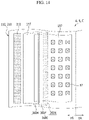
- FIG. 12 , FIG. 13 , and FIG. 14 are an enlarged layout view of a region A, a region B, or a region C as a part of a peripheral area of the display device shown in FIG. 3 , respectively.
- the display device 1 is the same as most of the embodiment shown in FIG. 1 to FIG. 8 , however the inclination portion 360N of the peripheral portion 360E of the pixel definition layer 360 does not overlap the holes 97 of the voltage transmission electrode 197.
- the inclination portion 360N forms the concave inclination surface and the height of the inclination surface 36S thereof is decreased, and the impact wave may be dispersed or offset.
- the concave inclination surface of the inclination portion 360N may be further concave compared with the case that the inclination portion 360N does not overlap the holes 97, as shown in FIG. 12 .
- the display device 1 is the same as most of the embodiment shown in FIG. 1 to FIG. 8 , however the shape of the spacer 360F of the peripheral portion 360E of the pixel definition layer 360 and the inclination portion 360N may be different.
- the edge that is not connected to the main portion 360H among the edges of the spacer 360F of the peripheral portion 360E may be a substantially straight line.
- the edge connected to the main portion 360H and the edge that is not connected to the main portion 360H may extend to be substantially parallel. Accordingly the inclination portion 360N extending to be parallel to at least one among the upper side edge E1, the right side edge E3, and the left side edge E4 of the encapsulation substrate 210 may be entirely connected.
- the edge connected to the spacer 360F of the inclination portion 360N and the edge that is not connected to the spacer 360F may extend to be substantially parallel.
- the inclination portion 360N may have the straight line shape extending to be parallel to at least one among the upper side edge E1, the right side edge E3, and the left side edge E4 of the encapsulation substrate 210.
- the inclination surface 36S of the inclination portion 360N is lowered far from the portion connected to the spacer 360F.
- the inclination surface 36S of the inclination portion 360N may be lowered toward the display area DA.
- the slope of the tangent line for the inclination surface 36S of the inclination portion 360N has the decreased absolute value farther away from the portion connected to the spacer 360F, that is, to the display area DA, such that the inclination surface 36S of the inclination portion 360N may form the concave curved surface.
- the edge of the inclination portion 360N may have the shape such as the straight dune.
- the inclination portion 360N may overlap the portion of the plurality of holes 97 of the voltage transmission electrode 197, and in detail, the holes 97 of one column disposed closest to the voltage transmission line 177.
- the display device 1 is the same as most of the embodiment shown in FIG. 13 , however the inclination portion 360N of the peripheral portion 360E of the pixel definition layer 360 does not overlap the holes 97 of the voltage transmission electrode 197.
- the inclination portion 360N also forms the concave inclination surface and the concave inclination surface 36S thereof may disperse and offset the impact wave.
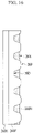
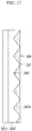
- FIG. 15 , FIG. 16 , FIG. 17 , FIG. 18 , FIG. 19 , and FIG. 20 are top plan views showing a plane shape of a peripheral portion of a pixel definition layer positioned in a peripheral area of a display device according to embodiments
- FIG. 21 is a photo showing an arrangement of a part of a peripheral area of a display device according to an embodiment.
- the peripheral portion of the pixel definition layer 360 is the same as most of the peripheral portion 360E of the embodiment shown in FIG. 1 to FIG. 8 .
- FIG. 15 is an example in which the recess portion 36D of the spacer 360F, the edge side of the convex portion 36P, and the edge of the inclination portion 360N are the quadrangle or the straight line.
- the peripheral portion of the pixel definition layer 360 is the same as most of the peripheral portion 360E of the embodiment shown in FIG. 1 to FIG. 8 , however the recess portion 36D of the spacer 360F and the edge side of the convex portion 36P form at least a partial curved line shape. Accordingly, the edge of the inclination portion 360N adjacent to the spacer 360F may also be formed of the curved line shape. Each outer edge 36N of the plurality of portions of the inclination portion 360N divided by the convex portion 36P of the spacer 360F may be formed of the straight line shape. Referring to FIG. 16 , the outside edge of the convex portion 36P of the spacer 360F may be positioned outside the extending line of the outer edge 36N of the plurality of the portions of the inclination portion 360N, however it is not limited thereto.
- the peripheral portion of the pixel definition layer 360 is the same as most of the peripheral portion 360E of the embodiment shown in FIG. 1 to FIG. 8 , however a boundary line of the spacer 360F and the inclination portion 360N have a sawtooth shape or a zigzag shape. Accordingly, the edge of the inclination portion 360N adjacent to the spacer 360F may be also formed of the sawtooth shape or the zigzag shape.
- Each outer edge 36N of the plurality of portions of the inclination portion 360N divided by the convex portion 36P of the spacer 360F may be formed of the substantially straight line shape. Referring to FIG. 17 , an apex of the convex portion 36P of the spacer 360F may be aligned to the extending line of the outer edge 36N of the plurality of portions of the inclination portion 360N, however it is not limited thereto.
- the peripheral portion of the pixel definition layer 360 is the same as most of the peripheral portion 360E of the embodiment shown in FIG. 1 to FIG. 8 , however the planar length of the convex portion 36P of the spacer 360F is not uniform.
- the convex portion 36P of the long length and the convex portion 36P of the short length may be alternately disposed according to the extending direction of the spacer 360F.
- the peripheral portion of the pixel definition layer 360 is the same as most of the peripheral portion 360E of the embodiment shown in FIG. 1 to FIG. 8 or the embodiment shown in FIG. 15 .
- FIG. 19 shows an example in which each portion of the inclination portion 360N is disposed corresponding to the holes 97 of the voltage transmission electrode 197 to overlap the holes 97 when the inclination portion 360N is divided into the plurality of portions by the convex portion 36P of the spacer 360F. Furthermore, the holes 97 adjacent to the holes 97 overlapping the inclination portion 360N are aligned with the holes 97 overlapping the inclination portion 360N, thereby forming the approximate matrix shape.
- the peripheral portion of the pixel definition layer 360 is the same as most of the embodiment shown in FIG. 19 , however the holes 97 adjacent to the holes 97 overlapping the inclination portion 360N are not aligned, but are shifted from the holes 97 overlapping the inclination portion 360N. That is, the holes 97 adjacent to the holes 97 overlapping the inclination portion 360N may be disposed on the line parallel to the space between the holes 97 overlapping the inclination portion 360N.
- FIG. 21 shows the plane shape of the display device corresponding to FIG. 20 .
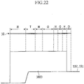
- FIG. 22 is a cross-sectional view of a coating layer and a photomask for a pixel definition layer in one process of a manufacturing method of a display device according to an embodiment of the invention
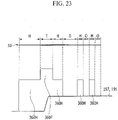
- FIG. 23 is a cross-sectional view of a pixel definition layer in the process shown in FIG. 22 in a process of a manufacturing method of a display device according to an embodiment of the invention
- FIG. 24 is a cross-sectional view of a pixel definition layer in the process shown in FIG. 23 in a process of a manufacturing method of a display device according to an embodiment of the invention.
- the buffer layer 111, the semiconductor layer, the gate insulating layer 140, the plurality of gate conductors, the first passivation layer 180a, the plurality of data conductors, and the second passivation layer 180b are formed on the lower substrate 110 including the transparent glass or plastic, and the pixel electrode layer including the pixel electrode 191 and the voltage transmission electrode 197 is formed thereon.
- the pixel electrode layer includes the top surface having a high portion and a low portion formed by an following step, for example, a step due to the edge side surface 186 of the above-described second passivation layer 180b.
- the photosensitive material such as the polyacrylates resin or the polyimide resin is coated on the pixel electrode layer to form a coating layer 3600.
- the photomask 50 includes a transmissive part T where most of the light is transmitted, a semi-transmissive part H where the light is partially transmitted, and a light blocking portion O where most of the light is not transmitted.
- the semi-transmissive part H may include a pattern such as a slit or a lattice or may include a semi-transparent layer.
- the coating layer 3600 exposed through the photomask 50 is developed to form a main portion 360H and a spacer 360F.
- the coating layer 3600 has negative photosensitivity of which the portion that is not irradiated by the light is removed, the main portion 360H corresponding to the semi-transmissive part H of the photomask 50 and the spacer 360F corresponding to the transmissive part T of the photomask 50 are formed, and the coating layer 3600 corresponding to the light blocking portion O of the photomask 50 may be removed.
- the thickness of the spacer 360F is greater than the thickness of the main portion 360H.
- the main portion 360H is respectively positioned at both sides of the spacer 360F covering the edge of the voltage transmission electrode 197, and two main portions 360H are connected to the spacer 360F.
- the bottom surface of the main portion 360H connected to the left side of the spacer 360F may be lower than the bottom surface of the main portion 360H connected to the right side of the spacer 360F.
- the right side of the spacer 360F may be the side that is closer to the display area DA.
- the thickness of the main portion 360H connected to the left side of the spacer 360F may be greater than the thickness of the main portion 360H connected to the right side of the spacer 360F.
- the transmittance of the photomask 50 is conversely changed and the coating layer 3600 is exposed, thereby forming the main portion 360H and the spacer 360F.
- a hardening process of applying heat or ultraviolet rays to the main portion 360H and the spacer 360F is performed to form the pixel definition layer 360.
- the top surface of the main portion 360H connected to the left side of the spacer 360F covering the edge of the voltage transmission electrode 197 may be formed of the convex curved surface, and the top surface of the main portion 360H connected to the right side of the spacer 360F is formed of the concave inclination surface 36S, thereby forming the inclination portion 360N. This is one of the reasons that the thickness of the main portion 360H connected to the left side of the spacer 360F is relatively thick and the thickness of the main portion 360H connected to the right side of the spacer 360F is relatively thin.
- the concave inclination surface 36S of the inclination portion 360N may be further well formed.
Landscapes
- Engineering & Computer Science (AREA)
- Microelectronics & Electronic Packaging (AREA)
- Physics & Mathematics (AREA)
- Optics & Photonics (AREA)
- Geometry (AREA)
- Manufacturing & Machinery (AREA)
- Electroluminescent Light Sources (AREA)
- Devices For Indicating Variable Information By Combining Individual Elements (AREA)
Claims (12)
- Anzeigevorrichtung (1), umfassend:ein erstes Substrat (110), umfassend:einen Anzeigebereich (DA), der eine Mehrzahl von Pixeln umfasst, undeinen Randbereich (PA), der um den Anzeigebereich (DA) herum befindlich ist;ein zweites Substrat (210), das dem ersten Substrat (110) zugewandt ist;ein Dichtungsmittel (310), das zwischen dem ersten Substrat (110) und dem zweiten Substrat (210) ausgebildet und in dem Randbereich (PA) befindlich ist,einen Dünnfilmtransistor, der auf dem ersten Substrat (110) befindlich ist;eine Pixelelektrodenschicht, die auf dem Dünnfilmtransistor befindlich ist und eine Mehrzahl von Pixelelektroden, die in dem Anzeigebereich (DA) befindlich sind, umfasst; undeine Pixeldefinitionsschicht (360), die auf der Pixelelektrodenschicht befindlich ist und einen Randabschnitt (360E), der eine Spannungsübertragungselektrode (197) überlappt, umfasst,wobei der Randabschnitt (360E) Folgendes umfasst:einen Abstandshalter (360F);einen Neigungsabschnitt (360N), der mit dem Abstandshalter (360F) ausgebildet und an einer ersten Seite des Abstandshalters (360F) befindlich ist,einen Hauptabschnitt (360H), der mit dem Abstandshalter (360F) verbunden und an einer zweiten Seite des Abstandshalters (360F), die der ersten Seite gegenüberliegt, befindlich und dem Dichtungsmittel (310) zugewandt ist, undwobei eine Höhe einer oberen Fläche des Abstandshalters (360F) in Bezug auf das erste Substrat (110) höher als eine Höhe einer oberen Fläche des Hauptabschnittes (360H) und des Neigungsabschnittes (360N) ist,
dadurch gekennzeichnet, dass der Neigungsabschnitt (360N) eine konkave Neigungsfläche aufweist. - Anzeigevorrichtung (1) nach Anspruch 1, wobei
eine Dicke des Neigungsabschnittes (360N) kleiner als eine Dicke des Hauptabschnittes (360H) ist. - Anzeigevorrichtung (1) nach Anspruch 2, wobei
eine Höhe einer unteren Fläche des Hauptabschnittes (360H) niedriger als eine Höhe einer unteren Fläche des Neigungsabschnittes (360N) ist. - Anzeigevorrichtung (1) nach Anspruch 3, ferner umfassend:eine Spannungsübertragungsleitung (177), die in dem Randbereich (PA) befindlich ist und eine gemeinsame Spannung überträgt; undeine Passivierungsschicht (180b), die zwischen dem Dünnfilmtransistor und der Pixelelektrodenschicht befindlich ist,wobei die Passivierungsschicht (180b) eine Randseitenfläche, welche die Spannungsübertragungsleitung (177) freilegt, umfasst unddie Spannungsübertragungselektrode (197), die in dem Randbereich (PA) befindlich ist, einen ersten Abschnitt, der die Randseitenfläche der Passivierungsschicht (180b) abdeckt, und einen zweiten Abschnitt, der mit der Spannungsübertragungsleitung (177) verbunden ist, umfasst.
- Anzeigevorrichtung (1) nach Anspruch 4, wobei
der Abstandshalter (360F) mindestens einen Teil, der die Randseitenfläche der Passivierungsschicht (180b) abdeckt, umfasst und die Pixelelektrodenschicht die Spannungsübertragungselektrode (197) umfasst. - Anzeigevorrichtung (1) nach einem vorangehenden Anspruch, wobei
ein Rand des Abstandshalters (360F) an der ersten Seite eine Form mit Vorsprüngen und Vertiefungen aufweist und abwechselnd angeordnete Vertiefungsabschnitte und konvexe Abschnitte umfasst. - Anzeigevorrichtung (1) nach Anspruch 6, wobeider Neigungsabschnitt (360N) eine Mehrzahl von Abschnitten, die in einer Draufsicht in den Vertiefungsabschnitten befindlich sind, umfasst undjeder aus der Mehrzahl von Abschnitten, die in dem Neigungsabschnitt (360N) enthalten sind, eine konkave Neigungsfläche aufweist.
- Anzeigevorrichtung (1) nach Anspruch 7, wobeidie Spannungsübertragungselektrode (197) eine Mehrzahl von Löchern (97) umfasst undjeder aus der Mehrzahl der Abschnitte des Neigungsabschnittes (360N) sich entsprechend mit jedem der Löcher (97) überlappt.
- Anzeigevorrichtung (1) nach Anspruch 8, wobei
ein Loch, das einem den Neigungsabschnitt (360N) überlappenden ersten Loch aus der Mehrzahl von Löchern (97) benachbart ist, dazu angeordnet ist, mit dem ersten Loch ausgerichtet zu sein. - Anzeigevorrichtung (1) nach Anspruch 8, wobei
ein Loch, das einem den Neigungsabschnitt (360N) überlappenden ersten Loch aus der Mehrzahl von Löchern (97) benachbart ist, dazu angeordnet ist, gegenüber dem ersten Loch versetzt zu sein. - Anzeigevorrichtung (1) nach Anspruch 6, wobei
ein Rand des Abstandshalters (360F) an der ersten Seite, der die Form mit Vorsprüngen und Vertiefungen aufweist, einen ersten konvexen Abschnitt und einen zweiten konvexen Abschnitt, die voneinander verschiedene Längen aufweisen, umfasst. - Verfahren zur Herstellung einer Anzeigevorrichtung (1), umfassend:Ausbilden eines Dünnfilmtransistors auf einem ersten Substrat (110), das einen Anzeigebereich (DA) und einen Randbereich (PA) um den Anzeigebereich herum umfasst;Ausbilden, auf dem Dünnfilmtransistor, einer Pixelelektrodenschicht, die eine Mehrzahl von Pixelelektroden, die in dem Anzeigebereich (DA) befindlich sind, umfasst;Beschichten der Pixelelektrodenschicht mit einem lichtempfindlichen Material, um eine Beschichtungsschicht auszubilden;Belichten der Beschichtungsschicht (3600) unter Verwendung einer Fotomaske (50), die einen lichtdurchlässigen Teil (T), einen lichtblockierenden Teil (O) und einen halbdurchlässigen Teil (H) umfasst;Entwickeln der belichteten Beschichtungsschicht (3600); undAushärten der entwickelten Beschichtungsschicht (3600), um eine Pixeldefinitionsschicht (360) auszubilden, die einen Randabschnitt (360E), der eine Spannungsübertragungselektrode (197) überlappt, umfasst;Ausbilden eines Dichtungsmittels (310) in dem Randbereich (PA) zwischen dem ersten Substrat (110) und einem zweiten Substrat (210),wobei der Randabschnitt (360E) Folgendes umfasst:einen Abstandshalter (360F);einen Neigungsabschnitt (360N), der mit dem Abstandshalter (360F) verbunden und ausgebildet und an einer ersten Seite des Abstandshalters (360F) befindlich ist, undwobei der Neigungsabschnitt (360N) eine konkave Neigungsfläche aufweist; undeinen Hauptabschnitt (360H), der mit dem Abstandshalter (360F) verbunden und an einer zweiten Seite des Abstandshalters (360F), die der ersten Seite gegenüberliegt, befindlich ist,wobei der Hauptabschnitt (360H) an einer Seite, die dem Dichtungsmittel (310) zugewandt ist, befindlich ist undeine Höhe einer oberen Fläche des Abstandshalters (360F) in Bezug auf das erste Substrat (110) höher als eine Höhe einer oberen Fläche des Hauptabschnittes (360H) und des Neigungsabschnittes (360N) sein kann.
Applications Claiming Priority (1)
| Application Number | Priority Date | Filing Date | Title |
|---|---|---|---|
| KR1020150033310A KR102364863B1 (ko) | 2015-03-10 | 2015-03-10 | 표시 장치 및 그 제조 방법 |
Publications (2)
| Publication Number | Publication Date |
|---|---|
| EP3067953A1 EP3067953A1 (de) | 2016-09-14 |
| EP3067953B1 true EP3067953B1 (de) | 2022-07-27 |
Family
ID=54707595
Family Applications (1)
| Application Number | Title | Priority Date | Filing Date |
|---|---|---|---|
| EP15196452.5A Active EP3067953B1 (de) | 2015-03-10 | 2015-11-26 | Anzeigevorrichtung und herstellungsverfahren dafür |
Country Status (4)
| Country | Link |
|---|---|
| US (2) | US10269881B2 (de) |
| EP (1) | EP3067953B1 (de) |
| KR (1) | KR102364863B1 (de) |
| CN (2) | CN105977273B (de) |
Families Citing this family (34)
| Publication number | Priority date | Publication date | Assignee | Title |
|---|---|---|---|---|
| KR102364863B1 (ko) | 2015-03-10 | 2022-02-18 | 삼성디스플레이 주식회사 | 표시 장치 및 그 제조 방법 |
| KR102399416B1 (ko) * | 2015-05-26 | 2022-05-18 | 삼성디스플레이 주식회사 | 유기 발광 표시 장치 |
| KR102668184B1 (ko) * | 2016-07-25 | 2024-05-24 | 삼성디스플레이 주식회사 | 표시 장치 |
| KR102601207B1 (ko) | 2016-07-29 | 2023-11-13 | 삼성디스플레이 주식회사 | 표시장치 |
| KR102582466B1 (ko) * | 2016-09-21 | 2023-09-25 | 삼성디스플레이 주식회사 | 표시 장치 |
| KR102600186B1 (ko) * | 2016-12-30 | 2023-11-10 | 엘지디스플레이 주식회사 | 측변 구부림 구조를 갖는 곡면 표시장치 |
| CN107425126B (zh) * | 2017-04-27 | 2019-09-10 | 京东方科技集团股份有限公司 | 像素界定结构、有机发光器件及其封装方法、显示装置 |
| CN107104127B (zh) * | 2017-04-27 | 2019-11-22 | 上海天马有机发光显示技术有限公司 | 有机发光显示面板和显示装置 |
| KR102482408B1 (ko) * | 2017-05-19 | 2022-12-28 | 삼성디스플레이 주식회사 | 표시 장치 |
| US20200274097A1 (en) * | 2017-09-29 | 2020-08-27 | Sharp Kabushiki Kaisha | Display device, exposure device, and manufacturing method of display device |
| CN107871776B (zh) | 2017-10-31 | 2020-10-16 | 昆山国显光电有限公司 | 有机电致发光器件、显示器及移动通信设备 |
| KR102544242B1 (ko) | 2018-03-16 | 2023-06-19 | 삼성디스플레이 주식회사 | 표시 장치 |
| CN108520892B (zh) * | 2018-05-09 | 2021-01-05 | 京东方科技集团股份有限公司 | 显示面板及其制造方法、显示装置 |
| CN112106444B (zh) * | 2018-05-23 | 2024-06-28 | 夏普株式会社 | 显示装置及其制造方法 |
| KR102606941B1 (ko) * | 2018-05-31 | 2023-11-30 | 삼성디스플레이 주식회사 | 표시장치 |
| KR102607270B1 (ko) * | 2018-07-17 | 2023-11-28 | 삼성디스플레이 주식회사 | 표시 장치 |
| KR102621591B1 (ko) * | 2018-09-11 | 2024-01-08 | 삼성디스플레이 주식회사 | 디스플레이 장치 |
| KR102662722B1 (ko) | 2018-09-17 | 2024-05-02 | 삼성디스플레이 주식회사 | 표시장치 |
| CN109285962B (zh) * | 2018-09-25 | 2020-12-01 | 合肥鑫晟光电科技有限公司 | 显示基板及制造方法、显示装置 |
| KR102870255B1 (ko) * | 2018-12-31 | 2025-10-14 | 엘지디스플레이 주식회사 | 전계 발광 표시 장치 및 이의 제조 방법 |
| KR102801662B1 (ko) * | 2019-04-16 | 2025-04-30 | 삼성디스플레이 주식회사 | 폴딩 가능한 디스플레이 장치 및 그 제조방법 |
| CN119012830A (zh) | 2019-08-01 | 2024-11-22 | 京东方科技集团股份有限公司 | 显示基板及显示装置 |
| CN112805771B (zh) * | 2019-08-01 | 2023-04-04 | 京东方科技集团股份有限公司 | 显示基板及显示装置 |
| WO2021017011A1 (zh) * | 2019-08-01 | 2021-02-04 | 京东方科技集团股份有限公司 | 显示基板及显示装置 |
| US12238983B2 (en) | 2019-08-27 | 2025-02-25 | Boe Technology Group Co., Ltd. | Display substrate and manufacturing method thereof, and display device |
| EP4024465B1 (de) | 2019-08-27 | 2026-02-25 | BOE Technology Group Co., Ltd. | Anzeigesubstrat und herstellungsverfahren dafür sowie anzeigevorrichtung |
| US11974472B2 (en) * | 2019-08-27 | 2024-04-30 | Boe Technology Group Co., Ltd. | Display substrate and manufacturing method thereof, and display device |
| JP7343614B2 (ja) * | 2019-11-22 | 2023-09-12 | 京東方科技集團股▲ふん▼有限公司 | 表示基板及びその製造方法、表示装置 |
| KR102932432B1 (ko) * | 2019-12-27 | 2026-02-26 | 엘지디스플레이 주식회사 | 표시 장치 |
| KR102705561B1 (ko) * | 2020-01-29 | 2024-09-11 | 삼성디스플레이 주식회사 | 표시 장치 |
| US12446441B2 (en) * | 2020-06-08 | 2025-10-14 | Sharp Kabushiki Kaisha | Display device and display device manufacturing method |
| CN112002831B (zh) * | 2020-09-22 | 2025-06-17 | 京东方科技集团股份有限公司 | 显示装置及显示面板 |
| US20240431141A1 (en) * | 2021-11-05 | 2024-12-26 | Sharp Display Technology Corporation | Display device and method for manufacturing same |
| CN117204141B (zh) * | 2022-04-06 | 2026-03-10 | 京东方科技集团股份有限公司 | 显示面板和显示装置 |
Citations (1)
| Publication number | Priority date | Publication date | Assignee | Title |
|---|---|---|---|---|
| KR20130137455A (ko) * | 2012-06-07 | 2013-12-17 | 엘지디스플레이 주식회사 | 유기전계발광 표시소자 |
Family Cites Families (27)
| Publication number | Priority date | Publication date | Assignee | Title |
|---|---|---|---|---|
| JP3748786B2 (ja) * | 2000-06-19 | 2006-02-22 | アルプス電気株式会社 | 表示装置および画像信号の処理方法 |
| US6992439B2 (en) * | 2001-02-22 | 2006-01-31 | Semiconductor Energy Laboratory Co., Ltd. | Display device with sealing structure for protecting organic light emitting element |
| CN1229655C (zh) * | 2001-06-01 | 2005-11-30 | 精工爱普生株式会社 | 滤色膜层及电光学装置 |
| US7616322B2 (en) * | 2002-07-08 | 2009-11-10 | Zygo Corporation | Cyclic error compensation in interferometry systems |
| JP3884351B2 (ja) * | 2002-08-26 | 2007-02-21 | 株式会社 日立ディスプレイズ | 画像表示装置およびその製造方法 |
| KR100699996B1 (ko) | 2004-09-02 | 2007-03-26 | 삼성에스디아이 주식회사 | 회로 측정용 패드를 포함하는 유기전계발광표시장치와 그제조방법 |
| TWI460851B (zh) | 2005-10-17 | 2014-11-11 | 半導體能源研究所股份有限公司 | 半導體裝置及其製造方法 |
| WO2008038544A1 (fr) * | 2006-09-28 | 2008-04-03 | Jsr Corporation | Procédé de formation de film de couche inférieure de résist, composition de film de couche inférieure de résist pour une utilisation dans le procédé, et procédé de formation de motif. |
| KR20090013857A (ko) | 2007-08-03 | 2009-02-06 | 엘지디스플레이 주식회사 | 유기발광다이오드 표시장치 및 이의 제조 방법 |
| KR100875103B1 (ko) * | 2007-11-16 | 2008-12-19 | 삼성모바일디스플레이주식회사 | 유기 발광 디스플레이 장치 |
| US8350468B2 (en) | 2008-06-30 | 2013-01-08 | Samsung Display Co., Ltd. | Organic electroluminescence display including a spacer and method for fabricating the same |
| KR20100019666A (ko) * | 2008-08-11 | 2010-02-19 | 삼성전자주식회사 | 박막 트랜지스터 표시판, 이를 포함하는 액정 표시 장치, 그리고 액정 표시 장치의 제조 방법 |
| TWI361330B (en) * | 2008-11-03 | 2012-04-01 | Au Optronics Corp | Method for forming pixel structure of transflective liquid crystal display device |
| JP2010181534A (ja) * | 2009-02-04 | 2010-08-19 | Sumitomo Chemical Co Ltd | 表示装置用基板およびその製造方法 |
| JP5515522B2 (ja) | 2009-08-31 | 2014-06-11 | 大日本印刷株式会社 | 有機エレクトロルミネッセンス表示装置用カラーフィルタおよび有機エレクトロルミネッセンス表示装置 |
| JP5690280B2 (ja) * | 2009-10-15 | 2015-03-25 | パナソニック株式会社 | 表示パネル装置及びその製造方法 |
| KR101094278B1 (ko) | 2010-03-09 | 2011-12-19 | 삼성모바일디스플레이주식회사 | 유기 발광 표시 장치 |
| KR20120078954A (ko) * | 2011-01-03 | 2012-07-11 | 삼성모바일디스플레이주식회사 | 유기전계발광표시장치 및 그 제조방법 |
| KR101519916B1 (ko) * | 2011-04-07 | 2015-05-13 | 엘지디스플레이 주식회사 | 유기 전계 발광 표시 장치 및 그의 제조 방법 |
| KR101811027B1 (ko) * | 2011-07-07 | 2017-12-21 | 삼성디스플레이 주식회사 | 유기 발광 디스플레이 장치 |
| KR101463650B1 (ko) * | 2011-08-30 | 2014-11-20 | 엘지디스플레이 주식회사 | 유기발광표시장치 및 그 제조방법 |
| KR101521676B1 (ko) * | 2011-09-20 | 2015-05-19 | 엘지디스플레이 주식회사 | 유기발광 다이오드 표시장치 및 그의 제조방법 |
| KR101881083B1 (ko) * | 2011-11-09 | 2018-07-24 | 삼성디스플레이 주식회사 | 유기 발광 표시 장치 |
| KR102030799B1 (ko) * | 2013-03-11 | 2019-10-11 | 삼성디스플레이 주식회사 | 유기발광표시장치 |
| KR102151752B1 (ko) | 2013-08-05 | 2020-09-04 | 삼성디스플레이 주식회사 | 유기발광 디스플레이 장치 및 그 제조방법 |
| CN103545345B (zh) | 2013-11-11 | 2016-09-21 | 京东方科技集团股份有限公司 | 一种显示面板及其制备方法、显示装置 |
| KR102364863B1 (ko) | 2015-03-10 | 2022-02-18 | 삼성디스플레이 주식회사 | 표시 장치 및 그 제조 방법 |
-
2015
- 2015-03-10 KR KR1020150033310A patent/KR102364863B1/ko active Active
- 2015-09-22 US US14/861,904 patent/US10269881B2/en active Active
- 2015-11-26 EP EP15196452.5A patent/EP3067953B1/de active Active
- 2015-12-17 CN CN201510954169.5A patent/CN105977273B/zh active Active
- 2015-12-17 CN CN202011382352.XA patent/CN112349763B/zh active Active
-
2019
- 2019-03-27 US US16/366,066 patent/US11164925B2/en active Active
Patent Citations (1)
| Publication number | Priority date | Publication date | Assignee | Title |
|---|---|---|---|---|
| KR20130137455A (ko) * | 2012-06-07 | 2013-12-17 | 엘지디스플레이 주식회사 | 유기전계발광 표시소자 |
Also Published As
| Publication number | Publication date |
|---|---|
| US20160268356A1 (en) | 2016-09-15 |
| KR102364863B1 (ko) | 2022-02-18 |
| KR20160110669A (ko) | 2016-09-22 |
| CN105977273A (zh) | 2016-09-28 |
| US11164925B2 (en) | 2021-11-02 |
| US20190221625A1 (en) | 2019-07-18 |
| CN112349763B (zh) | 2024-11-12 |
| CN105977273B (zh) | 2020-12-18 |
| US10269881B2 (en) | 2019-04-23 |
| EP3067953A1 (de) | 2016-09-14 |
| CN112349763A (zh) | 2021-02-09 |
Similar Documents
| Publication | Publication Date | Title |
|---|---|---|
| US11164925B2 (en) | Display device and manufacturing method thereof | |
| KR102707257B1 (ko) | 표시 장치 | |
| KR102334393B1 (ko) | 표시 장치 | |
| US9853249B2 (en) | Display device including reflecting layer | |
| KR102035252B1 (ko) | 밀봉재를 포함하는 표시 장치 및 그 제조 방법 | |
| WO2018179213A1 (ja) | 表示装置およびその製造方法 | |
| KR20170080790A (ko) | 유기발광다이오드 표시장치 및 그의 제조 방법 | |
| US20250017038A1 (en) | Display device | |
| US11910634B2 (en) | Display device and manufacturing method thereof | |
| WO2019176457A1 (ja) | 有機el表示装置および有機el表示装置の製造方法 | |
| KR101826363B1 (ko) | 유기발광다이오드 표시장치 및 그 제조 방법 | |
| KR20200137846A (ko) | 표시 장치 | |
| WO2019043761A1 (ja) | 表示素子を備えた非可撓性基板及び可撓性表示装置の製造方法 | |
| US20260130083A1 (en) | Display apparatus | |
| KR20110067366A (ko) | 유기전계발광소자 | |
| KR20260016765A (ko) | 표시 장치 및 이의 제조 방법 | |
| KR20250166531A (ko) | 표시 장치 | |
| KR20260021347A (ko) | 표시 장치 | |
| KR20250104805A (ko) | 표시 장치 | |
| KR20260066355A (ko) | 표시 장치 | |
| KR20250125562A (ko) | 표시 장치 | |
| JP2025051747A (ja) | 表示装置 | |
| JP2026012631A (ja) | 表示装置 | |
| US20250204228A1 (en) | Display apparatus having light-emitting devices | |
| CN118900583A (zh) | 透明显示面板及显示装置 |
Legal Events
| Date | Code | Title | Description |
|---|---|---|---|
| PUAI | Public reference made under article 153(3) epc to a published international application that has entered the european phase |
Free format text: ORIGINAL CODE: 0009012 |
|
| AK | Designated contracting states |
Kind code of ref document: A1 Designated state(s): AL AT BE BG CH CY CZ DE DK EE ES FI FR GB GR HR HU IE IS IT LI LT LU LV MC MK MT NL NO PL PT RO RS SE SI SK SM TR |
|
| AX | Request for extension of the european patent |
Extension state: BA ME |
|
| STAA | Information on the status of an ep patent application or granted ep patent |
Free format text: STATUS: REQUEST FOR EXAMINATION WAS MADE |
|
| 17P | Request for examination filed |
Effective date: 20170313 |
|
| RBV | Designated contracting states (corrected) |
Designated state(s): AL AT BE BG CH CY CZ DE DK EE ES FI FR GB GR HR HU IE IS IT LI LT LU LV MC MK MT NL NO PL PT RO RS SE SI SK SM TR |
|
| STAA | Information on the status of an ep patent application or granted ep patent |
Free format text: STATUS: EXAMINATION IS IN PROGRESS |
|
| 17Q | First examination report despatched |
Effective date: 20191120 |
|
| GRAP | Despatch of communication of intention to grant a patent |
Free format text: ORIGINAL CODE: EPIDOSNIGR1 |
|
| STAA | Information on the status of an ep patent application or granted ep patent |
Free format text: STATUS: GRANT OF PATENT IS INTENDED |
|
| INTG | Intention to grant announced |
Effective date: 20220211 |
|
| RIN1 | Information on inventor provided before grant (corrected) |
Inventor name: CHOI, HYUN-JUN Inventor name: JO, MIN JUN Inventor name: NA, EUN JAE Inventor name: GO, JAE KYUNG |
|
| GRAS | Grant fee paid |
Free format text: ORIGINAL CODE: EPIDOSNIGR3 |
|
| GRAA | (expected) grant |
Free format text: ORIGINAL CODE: 0009210 |
|
| STAA | Information on the status of an ep patent application or granted ep patent |
Free format text: STATUS: THE PATENT HAS BEEN GRANTED |
|
| AK | Designated contracting states |
Kind code of ref document: B1 Designated state(s): AL AT BE BG CH CY CZ DE DK EE ES FI FR GB GR HR HU IE IS IT LI LT LU LV MC MK MT NL NO PL PT RO RS SE SI SK SM TR |
|
| REG | Reference to a national code |
Ref country code: CH Ref legal event code: EP |
|
| REG | Reference to a national code |
Ref country code: DE Ref legal event code: R096 Ref document number: 602015080013 Country of ref document: DE |
|
| REG | Reference to a national code |
Ref country code: AT Ref legal event code: REF Ref document number: 1507669 Country of ref document: AT Kind code of ref document: T Effective date: 20220815 |
|
| REG | Reference to a national code |
Ref country code: IE Ref legal event code: FG4D |
|
| REG | Reference to a national code |
Ref country code: NL Ref legal event code: FP |
|
| REG | Reference to a national code |
Ref country code: LT Ref legal event code: MG9D |
|
| REG | Reference to a national code |
Ref country code: DE Ref legal event code: R079 Ref document number: 602015080013 Country of ref document: DE Free format text: PREVIOUS MAIN CLASS: H01L0051520000 Ipc: H10K0050800000 |
|
| PG25 | Lapsed in a contracting state [announced via postgrant information from national office to epo] |
Ref country code: SE Free format text: LAPSE BECAUSE OF FAILURE TO SUBMIT A TRANSLATION OF THE DESCRIPTION OR TO PAY THE FEE WITHIN THE PRESCRIBED TIME-LIMIT Effective date: 20220727 Ref country code: RS Free format text: LAPSE BECAUSE OF FAILURE TO SUBMIT A TRANSLATION OF THE DESCRIPTION OR TO PAY THE FEE WITHIN THE PRESCRIBED TIME-LIMIT Effective date: 20220727 Ref country code: PT Free format text: LAPSE BECAUSE OF FAILURE TO SUBMIT A TRANSLATION OF THE DESCRIPTION OR TO PAY THE FEE WITHIN THE PRESCRIBED TIME-LIMIT Effective date: 20221128 Ref country code: NO Free format text: LAPSE BECAUSE OF FAILURE TO SUBMIT A TRANSLATION OF THE DESCRIPTION OR TO PAY THE FEE WITHIN THE PRESCRIBED TIME-LIMIT Effective date: 20221027 Ref country code: LV Free format text: LAPSE BECAUSE OF FAILURE TO SUBMIT A TRANSLATION OF THE DESCRIPTION OR TO PAY THE FEE WITHIN THE PRESCRIBED TIME-LIMIT Effective date: 20220727 Ref country code: LT Free format text: LAPSE BECAUSE OF FAILURE TO SUBMIT A TRANSLATION OF THE DESCRIPTION OR TO PAY THE FEE WITHIN THE PRESCRIBED TIME-LIMIT Effective date: 20220727 Ref country code: FI Free format text: LAPSE BECAUSE OF FAILURE TO SUBMIT A TRANSLATION OF THE DESCRIPTION OR TO PAY THE FEE WITHIN THE PRESCRIBED TIME-LIMIT Effective date: 20220727 Ref country code: ES Free format text: LAPSE BECAUSE OF FAILURE TO SUBMIT A TRANSLATION OF THE DESCRIPTION OR TO PAY THE FEE WITHIN THE PRESCRIBED TIME-LIMIT Effective date: 20220727 |
|
| REG | Reference to a national code |
Ref country code: AT Ref legal event code: MK05 Ref document number: 1507669 Country of ref document: AT Kind code of ref document: T Effective date: 20220727 |
|
| PG25 | Lapsed in a contracting state [announced via postgrant information from national office to epo] |
Ref country code: PL Free format text: LAPSE BECAUSE OF FAILURE TO SUBMIT A TRANSLATION OF THE DESCRIPTION OR TO PAY THE FEE WITHIN THE PRESCRIBED TIME-LIMIT Effective date: 20220727 Ref country code: IS Free format text: LAPSE BECAUSE OF FAILURE TO SUBMIT A TRANSLATION OF THE DESCRIPTION OR TO PAY THE FEE WITHIN THE PRESCRIBED TIME-LIMIT Effective date: 20221127 Ref country code: HR Free format text: LAPSE BECAUSE OF FAILURE TO SUBMIT A TRANSLATION OF THE DESCRIPTION OR TO PAY THE FEE WITHIN THE PRESCRIBED TIME-LIMIT Effective date: 20220727 Ref country code: GR Free format text: LAPSE BECAUSE OF FAILURE TO SUBMIT A TRANSLATION OF THE DESCRIPTION OR TO PAY THE FEE WITHIN THE PRESCRIBED TIME-LIMIT Effective date: 20221028 |
|
| PG25 | Lapsed in a contracting state [announced via postgrant information from national office to epo] |
Ref country code: SM Free format text: LAPSE BECAUSE OF FAILURE TO SUBMIT A TRANSLATION OF THE DESCRIPTION OR TO PAY THE FEE WITHIN THE PRESCRIBED TIME-LIMIT Effective date: 20220727 Ref country code: RO Free format text: LAPSE BECAUSE OF FAILURE TO SUBMIT A TRANSLATION OF THE DESCRIPTION OR TO PAY THE FEE WITHIN THE PRESCRIBED TIME-LIMIT Effective date: 20220727 Ref country code: DK Free format text: LAPSE BECAUSE OF FAILURE TO SUBMIT A TRANSLATION OF THE DESCRIPTION OR TO PAY THE FEE WITHIN THE PRESCRIBED TIME-LIMIT Effective date: 20220727 Ref country code: CZ Free format text: LAPSE BECAUSE OF FAILURE TO SUBMIT A TRANSLATION OF THE DESCRIPTION OR TO PAY THE FEE WITHIN THE PRESCRIBED TIME-LIMIT Effective date: 20220727 Ref country code: AT Free format text: LAPSE BECAUSE OF FAILURE TO SUBMIT A TRANSLATION OF THE DESCRIPTION OR TO PAY THE FEE WITHIN THE PRESCRIBED TIME-LIMIT Effective date: 20220727 |
|
| REG | Reference to a national code |
Ref country code: DE Ref legal event code: R097 Ref document number: 602015080013 Country of ref document: DE |
|
| PG25 | Lapsed in a contracting state [announced via postgrant information from national office to epo] |
Ref country code: SK Free format text: LAPSE BECAUSE OF FAILURE TO SUBMIT A TRANSLATION OF THE DESCRIPTION OR TO PAY THE FEE WITHIN THE PRESCRIBED TIME-LIMIT Effective date: 20220727 Ref country code: EE Free format text: LAPSE BECAUSE OF FAILURE TO SUBMIT A TRANSLATION OF THE DESCRIPTION OR TO PAY THE FEE WITHIN THE PRESCRIBED TIME-LIMIT Effective date: 20220727 |
|
| PLBE | No opposition filed within time limit |
Free format text: ORIGINAL CODE: 0009261 |
|
| STAA | Information on the status of an ep patent application or granted ep patent |
Free format text: STATUS: NO OPPOSITION FILED WITHIN TIME LIMIT |
|
| P01 | Opt-out of the competence of the unified patent court (upc) registered |
Effective date: 20230515 |
|
| PG25 | Lapsed in a contracting state [announced via postgrant information from national office to epo] |
Ref country code: MC Free format text: LAPSE BECAUSE OF FAILURE TO SUBMIT A TRANSLATION OF THE DESCRIPTION OR TO PAY THE FEE WITHIN THE PRESCRIBED TIME-LIMIT Effective date: 20220727 Ref country code: AL Free format text: LAPSE BECAUSE OF FAILURE TO SUBMIT A TRANSLATION OF THE DESCRIPTION OR TO PAY THE FEE WITHIN THE PRESCRIBED TIME-LIMIT Effective date: 20220727 |
|
| REG | Reference to a national code |
Ref country code: CH Ref legal event code: PL |
|
| 26N | No opposition filed |
Effective date: 20230502 |
|
| REG | Reference to a national code |
Ref country code: BE Ref legal event code: MM Effective date: 20221130 |
|
| PG25 | Lapsed in a contracting state [announced via postgrant information from national office to epo] |
Ref country code: LI Free format text: LAPSE BECAUSE OF NON-PAYMENT OF DUE FEES Effective date: 20221130 Ref country code: CH Free format text: LAPSE BECAUSE OF NON-PAYMENT OF DUE FEES Effective date: 20221130 |
|
| PG25 | Lapsed in a contracting state [announced via postgrant information from national office to epo] |
Ref country code: SI Free format text: LAPSE BECAUSE OF FAILURE TO SUBMIT A TRANSLATION OF THE DESCRIPTION OR TO PAY THE FEE WITHIN THE PRESCRIBED TIME-LIMIT Effective date: 20220727 Ref country code: LU Free format text: LAPSE BECAUSE OF NON-PAYMENT OF DUE FEES Effective date: 20221126 |
|
| PG25 | Lapsed in a contracting state [announced via postgrant information from national office to epo] |
Ref country code: IE Free format text: LAPSE BECAUSE OF NON-PAYMENT OF DUE FEES Effective date: 20221126 |
|
| PG25 | Lapsed in a contracting state [announced via postgrant information from national office to epo] |
Ref country code: BE Free format text: LAPSE BECAUSE OF NON-PAYMENT OF DUE FEES Effective date: 20221130 |
|
| PG25 | Lapsed in a contracting state [announced via postgrant information from national office to epo] |
Ref country code: HU Free format text: LAPSE BECAUSE OF FAILURE TO SUBMIT A TRANSLATION OF THE DESCRIPTION OR TO PAY THE FEE WITHIN THE PRESCRIBED TIME-LIMIT; INVALID AB INITIO Effective date: 20151126 |
|
| PG25 | Lapsed in a contracting state [announced via postgrant information from national office to epo] |
Ref country code: CY Free format text: LAPSE BECAUSE OF FAILURE TO SUBMIT A TRANSLATION OF THE DESCRIPTION OR TO PAY THE FEE WITHIN THE PRESCRIBED TIME-LIMIT Effective date: 20220727 |
|
| PG25 | Lapsed in a contracting state [announced via postgrant information from national office to epo] |
Ref country code: MK Free format text: LAPSE BECAUSE OF FAILURE TO SUBMIT A TRANSLATION OF THE DESCRIPTION OR TO PAY THE FEE WITHIN THE PRESCRIBED TIME-LIMIT Effective date: 20220727 Ref country code: IT Free format text: LAPSE BECAUSE OF FAILURE TO SUBMIT A TRANSLATION OF THE DESCRIPTION OR TO PAY THE FEE WITHIN THE PRESCRIBED TIME-LIMIT Effective date: 20220727 |
|
| PG25 | Lapsed in a contracting state [announced via postgrant information from national office to epo] |
Ref country code: BG Free format text: LAPSE BECAUSE OF FAILURE TO SUBMIT A TRANSLATION OF THE DESCRIPTION OR TO PAY THE FEE WITHIN THE PRESCRIBED TIME-LIMIT Effective date: 20220727 |
|
| PG25 | Lapsed in a contracting state [announced via postgrant information from national office to epo] |
Ref country code: MT Free format text: LAPSE BECAUSE OF FAILURE TO SUBMIT A TRANSLATION OF THE DESCRIPTION OR TO PAY THE FEE WITHIN THE PRESCRIBED TIME-LIMIT Effective date: 20220727 |
|
| PGFP | Annual fee paid to national office [announced via postgrant information from national office to epo] |
Ref country code: NL Payment date: 20251020 Year of fee payment: 11 |
|
| PG25 | Lapsed in a contracting state [announced via postgrant information from national office to epo] |
Ref country code: TR Free format text: LAPSE BECAUSE OF FAILURE TO SUBMIT A TRANSLATION OF THE DESCRIPTION OR TO PAY THE FEE WITHIN THE PRESCRIBED TIME-LIMIT Effective date: 20220727 |
|
| PGFP | Annual fee paid to national office [announced via postgrant information from national office to epo] |
Ref country code: DE Payment date: 20251020 Year of fee payment: 11 |
|
| PGFP | Annual fee paid to national office [announced via postgrant information from national office to epo] |
Ref country code: GB Payment date: 20251023 Year of fee payment: 11 |
|
| PGFP | Annual fee paid to national office [announced via postgrant information from national office to epo] |
Ref country code: FR Payment date: 20251021 Year of fee payment: 11 |