EP3066907B1 - Befestigungselement zur befestigung an einer leiterplatte sowie befestigungsvorrichtung und verfahren zum beabstandeten verbinden von leiterplatten mit einem derartigen befestigungselement - Google Patents
Befestigungselement zur befestigung an einer leiterplatte sowie befestigungsvorrichtung und verfahren zum beabstandeten verbinden von leiterplatten mit einem derartigen befestigungselement Download PDFInfo
- Publication number
- EP3066907B1 EP3066907B1 EP15788443.8A EP15788443A EP3066907B1 EP 3066907 B1 EP3066907 B1 EP 3066907B1 EP 15788443 A EP15788443 A EP 15788443A EP 3066907 B1 EP3066907 B1 EP 3066907B1
- Authority
- EP
- European Patent Office
- Prior art keywords
- fitting
- section
- circuit board
- arresting
- spacer
- Prior art date
- Legal status (The legal status is an assumption and is not a legal conclusion. Google has not performed a legal analysis and makes no representation as to the accuracy of the status listed.)
- Active
Links
Images


Classifications
-
- H—ELECTRICITY
- H05—ELECTRIC TECHNIQUES NOT OTHERWISE PROVIDED FOR
- H05K—PRINTED CIRCUITS; CASINGS OR CONSTRUCTIONAL DETAILS OF ELECTRIC APPARATUS; MANUFACTURE OF ASSEMBLAGES OF ELECTRICAL COMPONENTS
- H05K1/00—Printed circuits
- H05K1/02—Details
- H05K1/14—Structural association of two or more printed circuits
- H05K1/144—Stacked arrangements of planar printed circuit boards
-
- H—ELECTRICITY
- H05—ELECTRIC TECHNIQUES NOT OTHERWISE PROVIDED FOR
- H05K—PRINTED CIRCUITS; CASINGS OR CONSTRUCTIONAL DETAILS OF ELECTRIC APPARATUS; MANUFACTURE OF ASSEMBLAGES OF ELECTRICAL COMPONENTS
- H05K1/00—Printed circuits
- H05K1/18—Printed circuits structurally associated with non-printed electric components
- H05K1/182—Printed circuits structurally associated with non-printed electric components associated with components mounted in printed circuit boards [PCB], e.g. insert-mounted components [IMC]
- H05K1/184—Printed circuits structurally associated with non-printed electric components associated with components mounted in printed circuit boards [PCB], e.g. insert-mounted components [IMC] associated with components inserted in holes through the PCBs and wherein terminals of the components are connected to printed contacts on the walls of the holes or at the edges thereof or protruding over or into the holes
-
- H—ELECTRICITY
- H05—ELECTRIC TECHNIQUES NOT OTHERWISE PROVIDED FOR
- H05K—PRINTED CIRCUITS; CASINGS OR CONSTRUCTIONAL DETAILS OF ELECTRIC APPARATUS; MANUFACTURE OF ASSEMBLAGES OF ELECTRICAL COMPONENTS
- H05K1/00—Printed circuits
- H05K1/02—Details
- H05K1/14—Structural association of two or more printed circuits
- H05K1/141—One or more single auxiliary printed circuits mounted on a main printed circuit, e.g. modules, adapters
-
- F—MECHANICAL ENGINEERING; LIGHTING; HEATING; WEAPONS; BLASTING
- F16—ENGINEERING ELEMENTS AND UNITS; GENERAL MEASURES FOR PRODUCING AND MAINTAINING EFFECTIVE FUNCTIONING OF MACHINES OR INSTALLATIONS; THERMAL INSULATION IN GENERAL
- F16B—DEVICES FOR FASTENING OR SECURING CONSTRUCTIONAL ELEMENTS OR MACHINE PARTS TOGETHER, e.g. NAILS, BOLTS, CIRCLIPS, CLAMPS, CLIPS OR WEDGES; JOINTS OR JOINTING
- F16B21/00—Means for preventing relative axial movement of a pin, spigot, shaft or the like and a member surrounding it; Stud-and-socket releasable fastenings
- F16B21/06—Releasable fastening devices with snap-action
- F16B21/08—Releasable fastening devices with snap-action in which the stud, pin, or spigot has a resilient part
- F16B21/082—Releasable fastening devices with snap-action in which the stud, pin, or spigot has a resilient part the stud, pin or spigot having two resilient parts on its opposite ends in order to connect two elements
-
- F—MECHANICAL ENGINEERING; LIGHTING; HEATING; WEAPONS; BLASTING
- F16—ENGINEERING ELEMENTS AND UNITS; GENERAL MEASURES FOR PRODUCING AND MAINTAINING EFFECTIVE FUNCTIONING OF MACHINES OR INSTALLATIONS; THERMAL INSULATION IN GENERAL
- F16B—DEVICES FOR FASTENING OR SECURING CONSTRUCTIONAL ELEMENTS OR MACHINE PARTS TOGETHER, e.g. NAILS, BOLTS, CIRCLIPS, CLAMPS, CLIPS OR WEDGES; JOINTS OR JOINTING
- F16B5/00—Joining sheets or plates, e.g. panels, to one another or to strips or bars parallel to them
- F16B5/06—Joining sheets or plates, e.g. panels, to one another or to strips or bars parallel to them by means of clamps or clips
- F16B5/0607—Joining sheets or plates, e.g. panels, to one another or to strips or bars parallel to them by means of clamps or clips joining sheets or plates to each other
- F16B5/0621—Joining sheets or plates, e.g. panels, to one another or to strips or bars parallel to them by means of clamps or clips joining sheets or plates to each other in parallel relationship
- F16B5/065—Joining sheets or plates, e.g. panels, to one another or to strips or bars parallel to them by means of clamps or clips joining sheets or plates to each other in parallel relationship the plates being one on top of the other and distanced from each other, e.g. by using protrusions to keep contact and distance
-
- H—ELECTRICITY
- H05—ELECTRIC TECHNIQUES NOT OTHERWISE PROVIDED FOR
- H05K—PRINTED CIRCUITS; CASINGS OR CONSTRUCTIONAL DETAILS OF ELECTRIC APPARATUS; MANUFACTURE OF ASSEMBLAGES OF ELECTRICAL COMPONENTS
- H05K1/00—Printed circuits
- H05K1/02—Details
- H05K1/14—Structural association of two or more printed circuits
-
- H—ELECTRICITY
- H05—ELECTRIC TECHNIQUES NOT OTHERWISE PROVIDED FOR
- H05K—PRINTED CIRCUITS; CASINGS OR CONSTRUCTIONAL DETAILS OF ELECTRIC APPARATUS; MANUFACTURE OF ASSEMBLAGES OF ELECTRICAL COMPONENTS
- H05K1/00—Printed circuits
- H05K1/18—Printed circuits structurally associated with non-printed electric components
- H05K1/181—Printed circuits structurally associated with non-printed electric components associated with surface mounted components
-
- H—ELECTRICITY
- H05—ELECTRIC TECHNIQUES NOT OTHERWISE PROVIDED FOR
- H05K—PRINTED CIRCUITS; CASINGS OR CONSTRUCTIONAL DETAILS OF ELECTRIC APPARATUS; MANUFACTURE OF ASSEMBLAGES OF ELECTRICAL COMPONENTS
- H05K3/00—Apparatus or processes for manufacturing printed circuits
- H05K3/30—Assembling printed circuits with electric components, e.g. with resistors
- H05K3/32—Assembling printed circuits with electric components, e.g. with resistors electrically connecting electric components or wires to printed circuits
- H05K3/34—Assembling printed circuits with electric components, e.g. with resistors electrically connecting electric components or wires to printed circuits by soldering
- H05K3/341—Surface mounted components
-
- H—ELECTRICITY
- H05—ELECTRIC TECHNIQUES NOT OTHERWISE PROVIDED FOR
- H05K—PRINTED CIRCUITS; CASINGS OR CONSTRUCTIONAL DETAILS OF ELECTRIC APPARATUS; MANUFACTURE OF ASSEMBLAGES OF ELECTRICAL COMPONENTS
- H05K3/00—Apparatus or processes for manufacturing printed circuits
- H05K3/36—Assembling printed circuits with other printed circuits
- H05K3/368—Assembling printed circuits with other printed circuits parallel to each other
-
- H—ELECTRICITY
- H05—ELECTRIC TECHNIQUES NOT OTHERWISE PROVIDED FOR
- H05K—PRINTED CIRCUITS; CASINGS OR CONSTRUCTIONAL DETAILS OF ELECTRIC APPARATUS; MANUFACTURE OF ASSEMBLAGES OF ELECTRICAL COMPONENTS
- H05K7/00—Constructional details common to different types of electric apparatus
- H05K7/14—Mounting supporting structure in casing or on frame or rack
- H05K7/1417—Mounting supporting structure in casing or on frame or rack having securing means for mounting boards, plates or wiring boards
- H05K7/142—Spacers not being card guides
-
- F—MECHANICAL ENGINEERING; LIGHTING; HEATING; WEAPONS; BLASTING
- F16—ENGINEERING ELEMENTS AND UNITS; GENERAL MEASURES FOR PRODUCING AND MAINTAINING EFFECTIVE FUNCTIONING OF MACHINES OR INSTALLATIONS; THERMAL INSULATION IN GENERAL
- F16B—DEVICES FOR FASTENING OR SECURING CONSTRUCTIONAL ELEMENTS OR MACHINE PARTS TOGETHER, e.g. NAILS, BOLTS, CIRCLIPS, CLAMPS, CLIPS OR WEDGES; JOINTS OR JOINTING
- F16B37/00—Nuts or like thread-engaging members
- F16B37/08—Quickly-detachable or mountable nuts, e.g. consisting of two or more parts; Nuts movable along the bolt after tilting the nut
- F16B37/0807—Nuts engaged from the end of the bolt, e.g. axially slidable nuts
- F16B37/0842—Nuts engaged from the end of the bolt, e.g. axially slidable nuts fastened to the threaded bolt with snap-on-action, e.g. push-on nuts for stud bolts
-
- H—ELECTRICITY
- H05—ELECTRIC TECHNIQUES NOT OTHERWISE PROVIDED FOR
- H05K—PRINTED CIRCUITS; CASINGS OR CONSTRUCTIONAL DETAILS OF ELECTRIC APPARATUS; MANUFACTURE OF ASSEMBLAGES OF ELECTRICAL COMPONENTS
- H05K2201/00—Indexing scheme relating to printed circuits covered by H05K1/00
- H05K2201/04—Assemblies of printed circuits
- H05K2201/042—Stacked spaced PCBs; Planar parts of folded flexible circuits having mounted components in between or spaced from each other
-
- H—ELECTRICITY
- H05—ELECTRIC TECHNIQUES NOT OTHERWISE PROVIDED FOR
- H05K—PRINTED CIRCUITS; CASINGS OR CONSTRUCTIONAL DETAILS OF ELECTRIC APPARATUS; MANUFACTURE OF ASSEMBLAGES OF ELECTRICAL COMPONENTS
- H05K2201/00—Indexing scheme relating to printed circuits covered by H05K1/00
- H05K2201/10—Details of components or other objects attached to or integrated in a printed circuit board
- H05K2201/10227—Other objects, e.g. metallic pieces
- H05K2201/1031—Surface mounted metallic connector elements
-
- H—ELECTRICITY
- H05—ELECTRIC TECHNIQUES NOT OTHERWISE PROVIDED FOR
- H05K—PRINTED CIRCUITS; CASINGS OR CONSTRUCTIONAL DETAILS OF ELECTRIC APPARATUS; MANUFACTURE OF ASSEMBLAGES OF ELECTRICAL COMPONENTS
- H05K2201/00—Indexing scheme relating to printed circuits covered by H05K1/00
- H05K2201/20—Details of printed circuits not provided for in H05K2201/01 - H05K2201/10
- H05K2201/2036—Permanent spacer or stand-off in a printed circuit or printed circuit assembly
-
- H—ELECTRICITY
- H05—ELECTRIC TECHNIQUES NOT OTHERWISE PROVIDED FOR
- H05K—PRINTED CIRCUITS; CASINGS OR CONSTRUCTIONAL DETAILS OF ELECTRIC APPARATUS; MANUFACTURE OF ASSEMBLAGES OF ELECTRICAL COMPONENTS
- H05K2201/00—Indexing scheme relating to printed circuits covered by H05K1/00
- H05K2201/20—Details of printed circuits not provided for in H05K2201/01 - H05K2201/10
- H05K2201/209—Auto-mechanical connection between a component and a PCB or between two PCBs
Definitions
- the invention relates to a fastening element for attachment to a printed circuit board. Furthermore, the invention relates to a fastening device and a method for spaced connection of printed circuit boards with such a fastener.
- a fastening device with a spacer tube and a spacer sleeve is known.
- the spacer tube forms stops for a printed circuit board and the spacer sleeve.
- the circuit board, the spacer tube and the spacer sleeve are connected together.
- a housing for electronic components is known.
- a base plate is arranged, which has raised areas for mounting a printed circuit board.
- For attachment serve fasteners that are locked with the raised areas and the circuit board.
- the invention is therefore an object of the invention to provide a fastener that allows automated assembly to a circuit board in a simple manner.
- the fastener should in particular allow an electrically insulating connection between printed circuit boards.
- the fastening element can be connected in a simple and automated manner with a spacer element which serves for fastening to a first printed circuit board. Furthermore, the fastener can be locked by means of the second locking portion in a simple and automated manner with a second circuit board, so that the circuit boards are spaced apart.
- the middle section arranged between the fastening section and the latching section serves to form a first stop for connecting the first fastening section to the associated spacer element and to form a second stop for connecting or / and receiving the second circuit board at the second latching section.
- the fastening element is for the formation of the fastening portion and the locking portion made in particular of an elastic material, such as a plastic material.
- the mounting surface ensures a simple way automated assembly of the fastener.
- the fastening element can be automatically held and mounted in a simple manner.
- the fastener can be automatically connected to the associated spacer.
- the fastener can be kept automated with the associated spacer to connect the spacer in a simple and automated manner with the first circuit board.
- the mounting surface serves as a suction surface to hold the fastener pneumatically.
- a fastener according to claim 3 allows in a simple manner a locking of the second latching portion with a second circuit board. Due to the fact that the second latching section has a predetermined deformation point, in particular a predetermined breaking point, in the region of the mounting surface, a simple insertion of the second latching section into an associated one is achieved Recess on the second circuit board allows. Since the mounting surface is no longer needed when locking the second locking portion with a second circuit board, a deformation or a breakage of the mounting surface is not disadvantageous.
- a fastener according to claim 4 ensures in a simple manner a locking of the second latching portion with a second circuit board. Due to the fact that the at least two latching arms are connected at the end by a wall, the second latching section on the one hand forms a mounting surface. On the other hand, the at least two mutually spaced latching arms due to the Solldeformationsstelle, in particular the predetermined breaking point in a simple manner radially to a central longitudinal axis of the fastener displaced. Since the latching arms are flexibly displaceable, latching of the second latching section with a second printed circuit board is made possible in a simple manner. Preferably, the at least two latching arms are formed of a plastic material.
- a fastening element according to claim 5 ensures in a simple manner a locking of the fastening portion designed as a first latching portion with a spacer element.
- the at least one first latching projection extends in the radial direction, starting from the support pin.
- the at least one first latching projection is lamellar, threaded and / or plate-like.
- a fastener according to claim 6 ensures in a simple manner a secure attachment of the fastener to the associated spacer.
- a fastener according to claim 7 ensures a simple automated connection of the fastener with the associated spacer. Characterized in that the mounting portion tapers to its free end, this can be easily and safely inserted into an associated recess of the spacer.
- a fastener according to claim 8 ensures a simple automated attachment of a second circuit board to the second latching portion. Characterized in that the at least one second latching projection tapers in the direction of a free end, the second latching portion can be easily and safely inserted into an associated recess of the second printed circuit board.
- a fastener according to claim 9 ensures a simple and automated connection to a first circuit board.
- a spacer element connected to the fastening element is preferably soldered to a first printed circuit board.
- the spacer has a high temperature. Since the spacer is in contact with the fastener, the fastener is also subjected to a high temperature.
- the temperature-resistant plastic material prevents damage to the fastener. Temperature resistant means in particular that no softening of the plastic material takes place up to a minimum temperature.
- the fastener is preferably formed of a high temperature plastic material such as LCP (LCP: Liquid Crystal Polymer).
- a fastener according to claim 10 allows an electrically insulating connection between two circuit boards.
- a fastener according to claim 11 ensures in a simple manner a reliable attachment.
- the fastener is also easy to produce.
- the attachment portion and / or the Rastaites are particularly designed such that the associated connection with the spacer or the circuit board is fixed or detachable.
- the invention is further based on the object to provide a fastening device which allows a simple, flexible and automated manner a spaced connection of printed circuit boards.
- the first attachment portion of the fastener is connected to the spacer.
- the connection between the attachment portion and the spacer element may be formed positively, positively and / or cohesively.
- the connection may be formed as a latching connection, screw connection, connection, adhesive connection and / or injection-molded connection.
- the attachment portion is preferably arranged in a recess of the spacer and secured therein. The recess is formed for example as a through hole or blind hole.
- the distance of the circuit boards to be connected can be specified in a simple and flexible manner by the length of the spacer element.
- the spacer element is formed separately from the first printed circuit board, that is not in one piece with the first printed circuit board.
- the spacer element is attached to the associated fastener to a first circuit board. Subsequently, a second circuit board can be locked with the fastening element.
- a fastening device ensures in a simple and reliable manner attachment of the spacer to the first circuit board.
- the metal is for example steel or brass.
- SMD Surface Mounted Device
- the advantages of the method according to the invention correspond to the already described advantages of the fastening element according to the invention and the fastening device according to the invention.
- the respective fastener may be connected to the associated spacer before or after the spacer has been attached or soldered to the first circuit board.
- the respective fastening element is first connected to an associated spacer element to a fastening device and then attached or soldered to the spacer on the first circuit board.
- the method according to the invention can in particular also be developed with the features of claims 12 and 13.
- a fastening device 1 serves for the spaced connection of a first printed circuit board 2 with a second printed circuit board 3.
- the fastening device 1 comprises a fastening element 4 which is positively connected to an associated spacer element 5.
- the fastening element 4 has a fastening section designed as a first latching section 6 and a second latching section 7, between which a middle section 8 is arranged.
- the locking portions 6, 7 are integrally formed with the central portion 8. Furthermore, the Locking sections 6, 7 arranged on the central portion 8, that the fastening element 4 has a central longitudinal axis 9.
- the latching sections 6, 7 and the middle section 8 are formed from a plastic material which is resistant up to a temperature of at least 240 ° C, in particular of at least 260 ° C, and in particular of at least 280 ° C.
- the plastic material is electrically insulating.
- the plastic material is an LCP (LCP: Liquid Crystal Polymer) plastic.
- the middle section 8 is formed by a circular disc 10 which forms a first stop 11 for the spacer element 5 on a front side facing the first latching section 6 and a second stop 12 for the second printed circuit board 3 on a front side facing the second latching section 7.
- the middle section 8 extends substantially perpendicular to the central longitudinal axis 9.
- a support pin 13 extends concentrically to the central longitudinal axis 9.
- the support pin 13 has a cylindrical trunnion base body 14, at the end a trunnion tip 15 is arranged so that the support pin 13 in the direction of a free end 16 rejuvenated.
- a plurality of first locking projections 18 are arranged on both sides of the trunnion base body 14, which are arranged spaced from one another along the central longitudinal axis 9.
- the first locking projections 18 are formed lamellar or plate-like. alternative
- the first latching projections 18 may be formed in a thread-like manner.
- the first latching projections 18 extend substantially along half the circumference of the trunnion base body 14.
- the trunnion 13 and the associated first latching projections 18 form the first latching section 6.
- the second latching portion 7 extends from the central portion 8 concentric with the central longitudinal axis 9.
- the second latching portion 7 comprises two latching arms 19, 20 which are spaced from each other at the central portion 8 and define a slot-shaped free space 21 between them. Due to the spaced arrangement, the latching arms 19, 20 are flexibly displaceable endwise in the radial direction.
- the latching arms 19, 20 are connected at the end by a wall 22 delimiting the free space 21.
- the wall 22 is formed so thin that it forms a desired deformation point, which allows a displacement of the latching arms 19, 20 in the radial direction.
- the wall 22 is so thin that it forms a predetermined breaking point, so that the wall 22 is destroyed in a radial displacement of the latching arms 19, 20.
- the locking arms 19, 20 are flat. Because the wall 22 extends flush between the latching arms 19, 20, the second latching section 7 forms a planar mounting surface A at the end.
- the mounting surface A extends substantially perpendicular to the central longitudinal axis 9.
- the mounting surface A is formed in particular circular. Preferably, A ⁇ 3 mm 2 , in particular A ⁇ 4.5 mm 2 , and in particular A ⁇ 6 mm 2 . The desired deformation point or predetermined breaking point is thus formed in the region of the mounting surface A.
- the latching arms 19, 20 each have a latching arm base body 23 and a latching arm tip 24 arranged thereon.
- the respective latching arm base body 23 and the associated latching arm tip 24 are formed in cross section in the form of a circle segment.
- the respective latching arm basic body 23 has a constant radius along the central longitudinal axis 9, so that the respective latching arm basic body 23 is designed in the form of a substantially half cylinder.
- the radius of the respective latching arm tip 24 decreases along the central longitudinal axis 9 toward the free end 30, so that the second latching section 7 tapers in the direction of the mounting surface A.
- the latching arm tip 24 immediately adjacent to the associated latching arm base body 23 has a larger radius
- the latching arm tip 24 forms with the associated latching arm base 23 a respective second latching projection 25.
- the respective second latching projection 25 forms an associated third stop 26 on a front side facing the middle section 8.
- the respective stop 26 has the shape of a ring portion.
- the spacer 5 has a spacer portion 27 and an integrally formed therewith insertion portion 28.
- the spacer section 27 and the insertion section 28 are hollow cylindrical and define a latching recess 29.
- the latching recess 29 extends along a central longitudinal axis 9 'through the spacer element 5.
- the spacer element 5 has an internal thread 31 for latching with the first Locking projections 18 on.
- the spacer section 27 has a larger radius than the insertion section 28, so that the spacer element 5 forms an annular insertion stop 32.
- the spacer section 27 forms an annular stop on a side facing away from the insertion section 28 33 out.
- the spacer 5 is for soldering to the first circuit board 2 made of a metal, in particular steel or brass.
- the circuit boards 2, 3 are connected by a plurality of fastening devices 1 spaced apart.
- fastening devices 1 spaced apart.
- the fastening device 1 is produced from the fastening element 4 and the associated spacer element 5.
- the first latching portion 6 is inserted into the latching recess 29, whereby the first latching projections 18 engage in the internal thread 31.
- the trunnion tip 15 insertion is facilitated. The insertion is stopped when the stops 11 and 33 abut against each other.
- the spacer 5 is provided as a separate component.
- a plurality of similar spacer elements 5 are available with a different length L, so that depending on the desired distance between the circuit boards 2, 3, a spacer element 5 with a suitable length L can be selected.
- the locking of the fastener 4 with the associated spacer 5 can be done manually or automatically.
- An automated latching takes place, for example, such that a plurality of fastening elements 4 are strapped and associated spacer elements 5 are equipped fully automatically.
- the automated locking can for example be such that the fastener 4 is held pneumatically on the flat mounting surface A and is introduced by means of a suitable handling system with the first latching portion 6 in the recess 29.
- the spacer element 5 is held mechanically by means of the handling system, for example.
- the fastening device 1 is pneumatically held on the mounting surface A and introduced by means of a handling system of the insertion section 28 of the spacer 5 in an associated insertion opening 34 in the first circuit board 2.
- the insertion is stopped by the insertion stopper 32.
- the metallic spacer 5 is then soldered to the first circuit board 2 by a solder 35 corresponding to an SMD device (SMD: Surface Mounted Device). If necessary, even further SMD components can be soldered to the first printed circuit board 2 in this soldering process.
- the solder 35 establishes a firm connection between the metallic spacer 5 and the first printed circuit board 2. Characterized in that the fastening element 4 is formed of a high temperature resistant plastic material, the fastener 4 is not damaged due to the soldering process.
- the second circuit board 3 is connected to the fastening element 4.
- the second circuit board 3 is gripped manually or automatically and moved in the direction of the central longitudinal axis 9, that the second latching portion 7 is inserted into a continuous recess 36 of the second circuit board 3.
- the latching arms 19, 20 are displaced radially in the direction of the central longitudinal axis 9, so that the wall 22 is deformed or destroyed due to the training as Solldeformationsstelle or predetermined breaking point.
- the latching arm tips 24 can thus be guided in a simple manner through the recess 36.
- the movement of the second circuit board 3 along the central longitudinal axis 9 is stopped, when the second circuit board 3 abuts against the stop 12.
- the axial length of the latching arm base body 23 is adapted so that when striking the latching arm tips 24 are completely guided by the recess 36, so that the third stops 26 form a counter-stop for the second circuit board 3.
- the axial length of the latching arm base body 23 approximately equal to the thickness of the second circuit board 3.
- the elastic latching arms 19, 20 move away again in the radial direction of the central longitudinal axis 9.
- the radius of the latching arm base body 23 substantially corresponds to the radius of the recess 36, so that the second circuit board 3 bears transversely to the central longitudinal axis 9 against the latching arm base body 23 and is held securely.
- the second latching section 7 is securely fastened to the second circuit board 3 in this way in the axial and radial directions.
- the second circuit board 3 is formed such that the recess 36 'widens in the direction of a side facing away from the first circuit board 2, then the second circuit board 3 bears against the stop 12 and is secured in the radial direction. In the axial direction, the second circuit board 3 is held in position by gravity.
- This alternative embodiment of the second circuit board 3 and the recess 36 ' is in Fig. 1 shown as a dashed line.
- the second latching portion 7 has a cylindrical base body 37 and a circular cross-section tip 38.
- the tip 38 forms the end of the planar mounting surface A from.
- the tip 38 forms a second latching projection 25 with a third stop 26.
- the fastener 4 is made of an elastic material, in particular of an elastic plastic or rubber material, so that the second latching portion 7 can be inserted through the recess 36.
- the attachment portion 6 is non-positively and / or materially connected to the spacer 5.
- the fastening section 6 has a fastening pin 39, which is connected to the middle section 8.
- the fastening pin 39 is arranged in a recess 40 of the spacer 5.
- the mounting pin 39 can taper according to the previous embodiments to its free end 16 out. Alternatively, the mounting pin 39 may be flat at the end.
- the recess 40 may be formed as a through hole or blind hole. In Fig. 6 is an education as blind hole illustrated.
- the fixing pin 39 may be connected to the spacer 5 by a press-fit connection, an adhesive connection or an injection-molded connection.
- the spacer element 5 serves as an insert part for an injection molding machine, wherein the fastening element 4 is connected to the spacer element 5 by injection molding directly during production.
- the distance mounting of printed circuit boards 2, 3 according to the invention thus ensures high process reliability and a high degree of automation when mounting two printed circuit boards at a defined distance.
- the mounting surface provides an integrated priming aid and ensures fully automatic assembly of the fastening device 1 on the first printed circuit board 2.
- the integrated priming aid does not have to be removed afterwards.
- the mounting surface is provided with a predetermined deformation point or predetermined breaking point, so that after insertion a snap-in function or latching function of the second latching section 7 is ensured.
Landscapes
- Engineering & Computer Science (AREA)
- Microelectronics & Electronic Packaging (AREA)
- General Engineering & Computer Science (AREA)
- Mechanical Engineering (AREA)
- Manufacturing & Machinery (AREA)
- Combinations Of Printed Boards (AREA)
- Mounting Of Printed Circuit Boards And The Like (AREA)
- Connection Of Plates (AREA)
- Insertion Pins And Rivets (AREA)
- Coupling Device And Connection With Printed Circuit (AREA)
Description
- Die vorliegende Patentanmeldung nimmt die Priorität der deutschen Patentanmeldung
DE 10 2014 222 951.0 in Anspruch, deren Inhalt durch Bezugnahme hierin aufgenommen wird. - Die Erfindung betrifft ein Befestigungselement zur Befestigung an einer Leiterplatte. Ferner betrifft die Erfindung eine Befestigungsvorrichtung sowie ein Verfahren zum beabstandeten Verbinden von Leiterplatten mit einem derartigen Befestigungselement.
- Aus der
DE 86 31 156 U1 ist eine Befestigungsvorrichtung mit einem Abstandsrohr und einer Distanzhülse bekannt. Das Abstandsrohr bildet Anschläge für eine Leiterplatte und die Distanzhülse aus. Mittels einer Schraube werden die Leiterplatte, das Abstandsrohr und die Distanzhülse miteinander verbunden. - Aus der
DE 10 2007 035 794 A1 ist ein Leiterplattenverbund bekannt, bei dem eine erste Leiterplatte mittels Abstandshaltern elektrisch leitend mit einer zweiten Leiterplatte verbunden ist. In die Abstandshalter aus Kunststoff sind Kontaktpins eingegossen. Ein umgebogener Kontaktpin wird mittels Lötmittel elektrisch leitend an der ersten Leiterplatte festgelegt, wohingegen ein zweiter Kontaktpin durch eine Montageöffnung in der zweiten Leiterplatte geführt und dort mit Hilfe von Lötmittel verlötet wird. Nachteilig ist, dass die Herstellung des Leiterplattenverbunds aufwendig ist und insbesondere keine elektrisch isolierende Verbindung herstellbar ist. - Aus der
EP 0 357 362 A2 ist ein Gehäuse für elektronische Bauteile bekannt. In dem Gehäuse ist eine Basisplatte angeordnet, die erhabene Bereiche zur Befestigung einer Leiterplatte aufweist. Zur Befestigung dienen Befestigungselemente, die mit den erhabenen Bereichen und der Leiterplatte verrastet sind. - Der Erfindung liegt somit die Aufgabe zugrunde, ein Befestigungselement zu schaffen, das in einfacher Weise eine automatisierte Montage an einer Leiterplatte ermöglicht. Das Befestigungselement soll insbesondere eine elektrisch isolierende Verbindung zwischen Leiterplatten ermöglichen.
- Diese Aufgabe wird durch ein Befestigungselement mit den Merkmalen des Anspruchs 1 gelöst. Mittels des ersten Befestigungsabschnitts kann das Befestigungselement in einfacher und automatisierter Weise mit einem Abstandselement verbunden werden, das zur Befestigung an einer ersten Leiterplatte dient. Weiterhin kann das Befestigungselement mittels des zweiten Rastabschnitts in einfacher und automatisierter Weise mit einer zweiten Leiterplatte verrastet werden, so dass die Leiterplatten beabstandet miteinander verbunden sind. Der zwischen dem Befestigungsabschnitt und dem Rastabschnitt angeordnete Mittelabschnitt dient zur Ausbildung eines ersten Anschlags für das Verbinden des ersten Befestigungsabschnitts mit dem zugehörigen Abstandselement sowie zur Ausbildung eines zweiten Anschlags für das Verbinden bzw. Verrasten und/oder die Aufnahme der zweiten Leiterplatte an dem zweiten Rastabschnitt. Das Befestigungselement ist zur Ausbildung des Befestigungsabschnitts und des Rastabschnitts insbesondere aus einem elastischen Material hergestellt, wie beispielsweise einem Kunststoffmaterial.
- Die Montagefläche gewährleistet in einfacher Weise eine automatisierte Montage des Befestigungselements. Durch die endseitig an dem zweiten Rastabschnitt angeordnete Montagefläche kann das Befestigungselement in einfacher Weise automatisiert gehalten und montiert werden. Beispielsweise kann das Befestigungselement automatisiert mit dem zugehörigen Abstandselement verbunden werden. Darüber hinaus kann das Befestigungselement mit dem damit verbundenen Abstandselement automatisiert gehalten werden, um das Abstandselement in einfacher und automatisierter Weise mit der ersten Leiterplatte zu verbinden. Die Montagefläche dient als Ansaugfläche, um das Befestigungselement pneumatisch zu halten.
- Ein Befestigungselement nach Anspruch 2 gewährleistet eine einfache automatisierte Montage. Durch die eben ausgebildete Montagefläche kann das Befestigungselement in einfacher Weise gehalten werden. Dies erfolgt pneumatisch. Für die Montagefläche A gilt insbesondere:
- A ≥ 3 mm2, insbesondere A ≥ 4,5 mm2, und insbesondere A ≥ 6 mm2. Die Montagefläche ist vorzugsweise kreisförmig ausgebildet. Vorzugsweise verläuft die Montagefläche senkrecht zu einer Mittellängsachse des Befestigungselements. Hierdurch wird in einfacher Weise eine Bewegung des Befestigungselements zum Verbinden mit dem Abstandselement und/oder zum Befestigen des Abstandselements an der ersten Leiterplatte in Richtung der Mittellängsachse ermöglicht.
- Ein Befestigungselement nach Anspruch 3 ermöglicht auf einfache Weise ein Verrasten des zweiten Rastabschnitts mit einer zweiten Leiterplatte. Dadurch, dass der zweite Rastabschnitt im Bereich der Montagefläche eine Solldeformationsstelle, insbesondere eine Sollbruchstelle aufweist, wird ein einfaches Einführen des zweiten Rastabschnitts in eine zugehörige Ausnehmung an der zweiten Leiterplatte ermöglicht. Da die Montagefläche beim Verrasten des zweiten Rastabschnitts mit einer zweiten Leiterplatte nicht mehr benötigt wird, ist eine Deformation bzw. ein Bruch der Montagefläche nicht nachteilig.
- Ein Befestigungselement nach Anspruch 4 gewährleistet auf einfache Weise ein Verrasten des zweiten Rastabschnitts mit einer zweiten Leiterplatte. Dadurch, dass die mindestens zwei Rastarme endseitig durch eine Wand verbunden sind, bildet der zweite Rastabschnitt einerseits eine Montagefläche aus. Andererseits sind die mindestens zwei zueinander beabstandeten Rastarme aufgrund der Solldeformationsstelle, insbesondere der Sollbruchstelle in einfacher Weise radial zu einer Mittellängsachse des Befestigungselements verlagerbar. Da die Rastarme flexibel verlagerbar sind, wird in einfacher Weise ein Verrasten des zweiten Rastabschnitts mit einer zweiten Leiterplatte ermöglicht. Vorzugsweise sind die mindestens zwei Rastarme aus einem Kunststoffmaterial ausgebildet.
- Ein Befestigungselement nach Anspruch 5 gewährleistet in einfacher Weise ein Verrasten des als ersten Rastabschnitts ausgebildeten Befestigungsabschnitts mit einem Abstandselement. Der mindestens eine erste Rastvorsprung erstreckt sich in radialer Richtung ausgehend von dem Tragzapfen. Beispielsweise ist der mindestens eine erste Rastvorsprung lamellen-, gewinde- und/oder tellerartig ausgebildet.
- Ein Befestigungselement nach Anspruch 6 gewährleistet in einfacher Weise eine sichere Befestigung des Befestigungselements an dem zugehörigen Abstandselement.
- Ein Befestigungselement nach Anspruch 7 gewährleistet ein einfaches automatisiertes Verbinden des Befestigungselements mit dem zugehörigen Abstandselement. Dadurch, dass sich der Befestigungsabschnitt zu seinem freien Ende verjüngt, kann dieser einfach und sicher in eine zugehörige Ausnehmung des Abstandselements eingeführt werden.
- Ein Befestigungselement nach Anspruch 8 gewährleistet eine einfache automatisierte Befestigung einer zweiten Leiterplatte an dem zweiten Rastabschnitt. Dadurch, dass sich der mindestens eine zweite Rastvorsprung in Richtung eines freien Endes verjüngt, kann der zweite Rastabschnitt einfach und sicher in eine zugehörige Ausnehmung der zweiten Leiterplatte eingeführt werden.
- Ein Befestigungselement nach Anspruch 9 gewährleistet eine einfache und automatisierte Verbindung mit einer ersten Leiterplatte. Ein mit dem Befestigungselement verbundenes Abstandselement wird vorzugsweise mit einer ersten Leiterplatte verlötet. Hierdurch weist das Abstandselement eine hohe Temperatur auf. Da das Abstandselement in Kontakt mit dem Befestigungselement ist, wird auch das Befestigungselement mit einer hohen Temperatur beaufschlagt. Das temperaturbeständige Kunststoffmaterial verhindert eine Beschädigung des Befestigungselements. Temperaturbeständig bedeutet insbesondere, dass bis zu einer Mindesttemperatur keine Erweichung des Kunststoffmaterials stattfindet. Das Befestigungselement ist vorzugsweise aus einem Hochtemperatur-Kunststoffmaterial, wie beispielsweise LCP (LCP: Liquid Crystal Polymer) ausgebildet.
- Ein Befestigungselement nach Anspruch 10 ermöglicht eine elektrisch isolierende Verbindung zwischen zwei Leiterplatten.
- Ein Befestigungselement nach Anspruch 11 gewährleistet in einfacher Weise eine zuverlässige Befestigung. Das Befestigungselement ist zudem einfach herstellbar. Der Befestigungsabschnitt und/oder der Rastaschnitt sind insbesondere derart ausgebildet, dass die zugehörige Verbindung mit dem Abstandselement bzw. der Leiterplatte fest oder wieder lösbar ist. Der Erfindung liegt ferner die Aufgabe zugrunde, eine Befestigungsvorrichtung zu schaffen, die auf einfache, flexible und automatisierte Weise ein beabstandetes Verbinden von Leiterplatten ermöglicht.
- Diese Aufgabe wird durch eine Befestigungsvorrichtung mit den Merkmalen des Anspruchs 12 gelöst. Die Vorteile der erfindungsgemäßen Befestigungsvorrichtung entsprechen den bereits beschriebenen Vorteilen des erfindungsgemäßen Befestigungselements. Der erste Befestigungsabschnitt des Befestigungselements ist mit dem Abstandselement verbunden. Die Verbindung zwischen dem Befestigungsabschnitt und dem Abstandselement kann formschlüssig, kraftschlüssig und/oder stoffschlüssig ausgebildet sein. Beispielsweise kann die Verbindung als Rastverbindung, Schraubverbindung, Verbindung, Klebverbindung und/oder Spritzgussverbindung ausgebildet sein. Der Befestigungsabschnitt ist vorzugsweise in einer Ausnehmung des Abstandselements angeordnet und darin befestigt. Die Ausnehmung ist beispielsweise als Durchgangsbohrung oder Sacklochbohrung ausgebildet. Durch die zweiteilige Ausbildung der Befestigungsvorrichtung kann der Abstand der zu verbindenden Leiterplatten in einfacher und flexibler Weise durch die Länge des Abstandselements vorgegeben werden. Hierzu kann beispielsweise aus mehreren gleichartigen Abstandselementen mit unterschiedlicher Länge je nach gewünschtem Abstand ein bestimmtes Abstandselement ausgewählt und mit dem Befestigungselement verbunden werden. Das Abstandselement ist separat von der ersten Leiterplatte ausgebildet, also nicht einteilig mit der ersten Leiterplatte. Das Abstandselement wird mit dem damit verbundenen Befestigungselement an einer ersten Leiterplatte befestigt. Anschließend kann eine zweite Leiterplatte mit dem Befestigungselement verrastet werden.
- Eine Befestigungsvorrichtung nach Anspruch 13 gewährleistet in einfacher und zuverlässiger Weise eine Befestigung des Abstandselements an der ersten Leiterplatte. Das Metall ist beispielsweise Stahl oder Messing. Dadurch, dass das Abstandselement aus einem Metall besteht, bildet die Befestigungsvorrichtung ein SMD-Bauelement (SMD: Surface Mounted Device) aus, das beispielsweise zusammen mit weiteren SMD-Bauelementen an der ersten Leiterplatte verlötet wird.
- Der Erfindung liegt ferner die Aufgabe zugrunde, ein Verfahren zu schaffen, das in einfacher, flexibler und automatisierter Weise ein beabstandetes Verbinden von Leiterplatten ermöglicht.
- Diese Aufgabe wird durch ein Verfahren mit den Merkmalen des Anspruchs 14 gelöst. Die Vorteile des erfindungsgemäßen Verfahrens entsprechen den bereits beschriebenen Vorteilen des erfindungsgemäßen Befestigungselements und der erfindungsgemäßen Befestigungsvorrichtung. Das jeweilige Befestigungselement kann mit dem zugehörigen Abstandselement bevor oder nachdem das Abstandselement an der ersten Leiterplatte befestigt bzw. verlötet wurde, verbunden werden. Vorzugsweise wird das jeweilige Befestigungselement zunächst mit einem zugehörigen Abstandselement zu einer Befestigungsvorrichtung verbunden und anschließend das Abstandselement an der ersten Leiterplatte befestigt bzw. verlötet. Das erfindungsgemäße Verfahren kann insbesondere auch mit den Merkmalen der Ansprüche 12 und 13 weitergebildet werden.
- Weitere Merkmale, Vorteile und Einzelheiten der Erfindung ergeben sich aus der nachfolgenden Beschreibung mehrerer Ausführungsbeispiele. Es zeigen:
- Fig. 1
- einen Schnitt durch eine Befestigungsvorrichtung gemäß einem ersten Ausführungsbeispiel, die zwei Leiterplatten beabstandet miteinander verbindet,
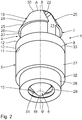
- Fig. 2
- eine perspektivische Ansicht der Befestigungsvorrichtung in
Fig. 1 , - Fig. 3
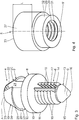
- eine perspektivische Ansicht eines Befestigungselements der Befestigungsvorrichtung in
Fig. 2 , - Fg. 4
- eine perspektivische Ansicht eines Abstandselements der Befestigungsvorrichtung in
Fig. 2 , - Fig. 5
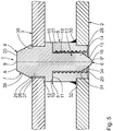
- einen Schnitt durch eine Befestigungsvorrichtung gemäß einem zweiten Ausführungsbeispiel, die zwei Leiterplatten beabstandet miteinander verbindet, und
- Fig. 6
- einen Schnitt durch eine Befestigungsvorrichtung gemäß einem dritten Ausführungsbeispiel, die zwei Leiterplatten beabstandet miteinander verbindet.
- Nachfolgend ist anhand der
Figuren 1 bis 4 ein erstes Ausführungsbeispiel beschrieben. Eine Befestigungsvorrichtung 1 dient zum beabstandeten Verbinden einer ersten Leiterplatte 2 mit einer zweiten Leiterplatte 3. Die Befestigungsvorrichtung 1 umfasst ein Befestigungselement 4, das mit einem zugehörigen Abstandselement 5 formschlüssig verbunden ist. - Das Befestigungselement 4 weist einen als ersten Rastabschnitt 6 ausgebildeten Befestigungsabschnitt und einen zweiten Rastabschnitt 7 auf, zwischen denen ein Mittelabschnitt 8 angeordnet ist. Die Rastabschnitte 6, 7 sind mit dem Mittelabschnitt 8 einteilig ausgebildet. Weiterhin sind die Rastabschnitte 6, 7 derart an dem Mittelabschnitt 8 angeordnet, dass das Befestigungselement 4 eine Mittellängsachse 9 aufweist.
- Die Rastabschnitte 6, 7 und der Mittelabschnitt 8 sind aus einem Kunststoffmaterial ausgebildet, das bis zu einer Temperatur von mindestens 240°C, insbesondere von mindestens 260°C, und insbesondere von mindestens 280°C beständig ist. Das Kunststoffmaterial ist elektrisch isolierend. Beispielsweise ist das Kunststoffmaterial ein LCP-Kunststoff (LCP: Liquid Crystal Polymer).
- Der Mittelabschnitt 8 ist durch eine kreisförmige Scheibe 10 gebildet, die an einer dem ersten Rastabschnitt 6 zugewandten Stirnseite einen ersten Anschlag 11 für das Abstandselement 5 und an einer dem zweiten Rastabschnitt 7 zugewandten Stirnseite einen zweiten Anschlag 12 für die zweite Leiterplatte 3 ausbildet. Der Mittelabschnitt 8 erstreckt sich im Wesentlichen senkrecht zu der Mittellängsachse 9.
- Ausgehend von dem Mittelabschnitt 8 erstreckt sich ein Tragzapfen 13 konzentrisch zu der Mittellängsachse 9. Der Tragzapfen 13 weist einen zylinderförmigen Tragzapfen-Grundkörper 14 auf, an dem endseitig eine Tragzapfen-Spitze 15 angeordnet ist, so dass sich der Tragzapfen 13 in Richtung eines freien Endes 16 verjüngt. An dem Tragzapfen-Grundkörper 14 sind einander relativ zu der Mittellängsachse 9 gegenüberliegende Tragzapfen-Stege 17 angeordnet, die entlang der Mittellängsachse 9 verlaufen und die Tragzapfen-Spitze 15 mit dem Mittelabschnitt 8 verbinden. Zwischen den Tragzapfen-Stegen 17 sind auf beiden Seiten des Tragzapfen-Grundkörpers 14 mehrere erste Rastvorsprünge 18 angeordnet, die entlang der Mittellängsachse 9 beabstandet zueinander angeordnet sind. Die ersten Rastvorsprünge 18 sind lamellenartig bzw. tellerartig ausgebildet. Alternativ können die ersten Rastvorsprünge 18 gewindeartig ausgebildet sein. Die ersten Rastvorsprünge 18 erstrecken sich im Wesentlichen entlang des halben Umfangs des Tragzapfen-Grundkörpers 14. Der Tragzapfen 13 und die zugehörigen ersten Rastvorsprünge 18 bilden den ersten Rastabschnitt 6 aus.
- Der zweite Rastabschnitt 7 erstreckt sich ausgehend von dem Mittelabschnitt 8 konzentrisch zu der Mittellängsachse 9. Der zweite Rastabschnitt 7 umfasst zwei Rastarme 19, 20, die beabstandet zueinander an dem Mittelabschnitt 8 angeordnet sind und zwischen sich einen schlitzförmigen Freiraum 21 begrenzen. Durch die beabstandete Anordnung sind die Rastarme 19, 20 endseitig in radialer Richtung flexibel verlagerbar. Die Rastarme 19, 20 sind endseitig durch eine den Freiraum 21 begrenzende Wand 22 verbunden. Die Wand 22 ist derart dünn ausgebildet, dass diese eine Solldeformationsstelle ausbildet, die eine Verlagerung der Rastarme 19, 20 in radialer Richtung zulässt. Vorzugsweise ist die Wand 22 derart dünn, dass diese eine Sollbruchstelle ausbildet, so dass die Wand 22 bei einer radialen Verlagerung der Rastarme 19, 20 zerstört wird.
- An einem freien Ende 30 des zweiten Rastabschnitts 7 sind die Rastarme 19, 20 eben ausgebildet. Dadurch, dass die Wand 22 bündig zwischen den Rastarmen 19, 20 verläuft, bildet der zweite Rastabschnitt 7 endseitig eine ebene Montagefläche A aus. Die Montagefläche A verläuft im Wesentlichen senkrecht zu der Mittellängsachse 9. Die Montagefläche A ist insbesondere kreisförmig ausgebildet. Vorzugsweise gilt: A ≥ 3 mm2, insbesondere A ≥ 4,5 mm2, und insbesondere A ≥ 6 mm2. Die Solldeformationsstelle bzw. Sollbruchstelle ist somit im Bereich der Montagefläche A ausgebildet.
- Die Rastarme 19, 20 weisen jeweils einen Rastarm-Grundkörper 23 und eine daran angeordnete Rastarm-Spitze 24 auf. Der jeweilige Rastarm-Grundkörper 23 und die zugehörige Rastarm-Spitze 24 sind im Querschnitt in Form eines Kreissegments ausgebildet. Der jeweilige Rastarm-Grundkörper 23 weist entlang der Mittellängsachse 9 einen konstanten Radius auf, so dass der jeweilige Rastarm-Grundkörper 23 in Form eines im Wesentlichen halben Zylinders ausgebildet ist. Demgegenüber nimmt der Radius der jeweiligen Rastarm-Spitze 24 entlang der Mittellängsachse 9 zu dem freien Ende 30 hin ab, so dass sich der zweite Rastabschnitt 7 in Richtung der Montagefläche A verjüngt. Dadurch, dass die jeweilige Rastarm-Spitze 24 unmittelbar benachbart zu dem zugehörigen Rastarm-Grundkörper 23 einen größeren Radius hat, bildet die Rastarm-Spitze 24 mit dem zugehörigen Rastarm-Grundkörper 23 einen jeweiligen zweiten Rastvorsprung 25 aus. Der jeweilige zweite Rastvorsprung 25 bildet an einer dem Mittelabschnitt 8 zugewandten Stirnseite einen zugehörigen dritten Anschlag 26 aus. Der jeweilige Anschlag 26 hat die Form eines Ringabschnitts.
- Das Abstandselement 5 weist einen Distanzabschnitt 27 und einen einteilig damit ausgebildeten Einführabschnitt 28 auf. Der Distanzabschnitt 27 und der Einführabschnitt 28 sind hohlzylinderförmig ausgebildet und begrenzen eine Rastausnehmung 29. Die Rastausnehmung 29 erstreckt sich entlang einer Mittellängsachse 9' durch das Abstandselement 5. An einer der Rastausnehmung 29 zugewandten Innenwand weist das Abstandselement 5 ein Innengewinde 31 zum Verrasten mit den ersten Rastvorsprüngen 18 auf. Der Distanzabschnitt 27 weist einen größeren Radius auf als der Einführabschnitt 28, so dass das Abstandselement 5 einen ringförmigen Einführanschlag 32 ausbildet. Darüber hinaus bildet der Distanzabschnitt 27 an einer dem Einführabschnitt 28 abgewandten Seite einen ringförmigen Anschlag 33 aus. Das Abstandselement 5 besteht zum Verlöten mit der ersten Leiterplatte 2 aus einem Metall, insbesondere aus Stahl oder Messing.
- Nachfolgend ist das beabstandete Verbinden der Leiterplatten 2, 3 im Einzelnen beschrieben. Die Leiterplatten 2, 3 werden mittels mehrerer Befestigungsvorrichtungen 1 beabstandet miteinander verbunden. Nachfolgend ist beispielhaft lediglich das Verbinden der Leiterplatten 2, 3 mittels einer der Befestigungsvorrichtungen 1 beschrieben.
- Zunächst wird aus dem Befestigungselement 4 und dem zugehörigen Abstandselement 5 die Befestigungsvorrichtung 1 hergestellt. Hierzu wird der erste Rastabschnitt 6 in die Rastausnehmung 29 eingeführt, wodurch die ersten Rastvorsprünge 18 in dem Innengewinde 31 verrasten. Durch die Tragzapfen-Spitze 15 wird das Einführen erleichtert. Das Einführen wird gestoppt, wenn die Anschläge 11 und 33 gegeneinander anliegen.
- Das Abstandselement 5 wird als separates Bauteil bereitgestellt. Vorzugsweise stehen mehrere gleichartige Abstandselemente 5 mit einer unterschiedlichen Länge L bereit, so dass je nach gewünschtem Abstand zwischen den Leiterplatten 2, 3 ein Abstandselement 5 mit einer geeigneten Länge L auswählbar ist. Das Verrasten des Befestigungselements 4 mit dem zugehörigen Abstandselement 5 kann manuell oder automatisiert erfolgen. Ein automatisiertes Verrasten erfolgt beispielsweise derart, dass mehrere Befestigungselemente 4 gegurtet sind und zugehörige Abstandselemente 5 vollautomatisch bestückt werden. Weiterhin kann das automatisierte Verrasten beispielsweise derart erfolgen, dass das Befestigungselement 4 an der ebenen Montagefläche A pneumatisch gehalten wird und mittels eines geeigneten Handhabungssystems mit dem ersten Rastabschnitt 6 in die Rastausnehmung 29 eingeführt wird. Das Abstandselement 5 wird hierbei mittels des Handhabungssystems beispielsweise mechanisch gehalten.
- Anschließend wird die erste Leiterplatte 2 an der Befestigungsvorrichtung 1 befestigt. Hierzu wird die Befestigungsvorrichtung 1 an der Montagefläche A pneumatisch gehalten und mittels eines Handhabungssystems der Einführabschnitt 28 des Abstandselements 5 in eine zugehörige Einführöffnung 34 in der ersten Leiterplatte 2 eingeführt. Das Einführen wird durch den Einführanschlag 32 gestoppt. Das metallische Abstandselement 5 wird daraufhin mit der ersten Leiterplatte 2 durch ein Lötmittel 35 entsprechend einem SMD-Bauelement (SMD: Surface Mounted Device) verlötet. Bei diesem Lötvorgang können ggf. auch noch weitere SMD-Bauelemente mit der ersten Leiterplatte 2 verlötet werden. Das Lötmittel 35 stellt eine feste Verbindung zwischen dem metallischen Abstandselement 5 und der ersten Leiterplatte 2 her. Dadurch, dass das Befestigungselement 4 aus einem hochtemperaturbeständigen Kunststoffmaterial ausgebildet ist, wird das Befestigungselement 4 aufgrund des Lötvorgangs nicht beschädigt.
- Anschließend wird die zweite Leiterplatte 3 mit dem Befestigungselement 4 verbunden. Hierzu wird die zweite Leiterplatte 3 manuell oder automatisch gegriffen und derart in Richtung der Mittellängsachse 9 bewegt, dass der zweite Rastabschnitt 7 in eine durchgehende Ausnehmung 36 der zweiten Leiterplatte 3 eingeführt wird. Beim Einführen werden die Rastarme 19, 20 radial in Richtung der Mittellängsachse 9 verlagert, so dass die Wand 22 aufgrund der Ausbildung als Solldeformationsstelle bzw. Sollbruchstelle deformiert bzw. zerstört wird. Die Rastarm-Spitzen 24 können so in einfacher Weise durch die Ausnehmung 36 geführt werden. Die Bewegung der zweiten Leiterplatte 3 entlang der Mittellängsachse 9 wird gestoppt, wenn die zweite Leiterplatte 3 gegen den Anschlag 12 anschlägt. Die axiale Länge der Rastarm-Grundkörper 23 ist derart angepasst, dass beim Anschlagen die Rastarm-Spitzen 24 vollständig durch die Ausnehmung 36 geführt sind, so dass die dritten Anschläge 26 einen Gegenanschlag für die zweite Leiterplatte 3 bilden. Hierzu entspricht die axiale Länge der Rastarm-Grundkörper 23 ungefähr der Dicke der zweiten Leiterplatte 3. Nachdem die Rastarm-Spitzen 24 vollständig durch die Ausnehmung 36 geführt sind, verlagern sich die elastischen Rastarme 19, 20 wieder in radialer Richtung von der Mittellängsachse 9 weg. Der Radius der Rastarm-Grundkörper 23 entspricht im Wesentlichen dem Radius der Ausnehmung 36, so dass die zweite Leiterplatte 3 quer zu der Mittellängsachse 9 gegen die Rastarm-Grundkörper 23 anliegt und sicher gehalten wird. Der zweite Rastabschnitt 7 wird auf diese Weise in axialer und radialer Richtung sicher an der zweiten Leiterplatte 3 befestigt.
- Ist die zweite Leiterplatte 3 derart ausgebildet, dass sich die Ausnehmung 36' in Richtung einer der ersten Leiterplatte 2 abgewandten Seite erweitert, so liegt die zweite Leiterplatte 3 gegen den Anschlag 12 an und ist in radialer Richtung gesichert. In axialer Richtung wird die zweite Leiterplatte 3 durch die Schwerkraft in Position gehalten. Diese alternative Ausgestaltung der zweiten Leiterplatte 3 und der Ausnehmung 36' ist in
Fig. 1 als gestrichelte Linie dargestellt. - Nachfolgend ist anhand von
Figur 5 ein zweites Ausführungsbeispiel beschrieben. Im Unterschied zu dem ersten Ausführungsbeispiel weist der zweite Rastabschnitt 7 einen zylinderförmigen Grundkörper 37 und eine im Querschnitt kreisförmige Spitze 38 auf. Die Spitze 38 bildet endseitig die ebene Montagefläche A aus. Weiterhin bildet die Spitze 38 einen zweiten Rastvorsprung 25 mit einem dritten Anschlag 26 aus. Das Befestigungselement 4 ist aus einem elastischen Material, insbesondere aus einem elastischen Kunststoff- oder Gummimaterial, so dass der zweite Rastabschnitt 7 durch die Ausnehmung 36 einführbar ist. Hinsichtlich des weiteren Aufbaus und der weiteren Funktionsweise wird auf das erste Ausführungsbeispiel verwiesen. - Nachfolgend ist anhand von
Fig. 6 ein drittes Ausführungsbeispiel beschrieben. Im Unterschied zu den vorangegangenen Ausführungsbeispielen ist der Befestigungsabschnitt 6 mit dem Abstandselement 5 kraftschlüssig und/oder stoffschlüssig verbunden. Der Befestigungsabschnitt 6 weist hierzu einen Befestigungszapfen 39 auf, der mit dem Mittelabschnitt 8 verbunden ist. Der Befestigungszapfen 39 ist in einer Ausnehmung 40 des Abstandselements 5 angeordnet. Der Befestigungszapfen 39 kann sich entsprechend den vorangegangenen Ausführungsbeispielen zu seinem freien Ende 16 hin verjüngen. Alternativ kann der Befestigungszapfen 39 endseitig eben ausgebildet sein. Die Ausnehmung 40 kann als Durchgangsbohrung oder Sacklochbohrung ausgebildet sein. InFig. 6 ist eine Ausbildung als Sacklochbohrung veranschaulicht. Der Befestigungszapfen 39 kann durch eine Presspassverbindung, eine Klebverbindung oder eine Spritzgussverbindung mit dem Abstandselement 5 verbunden sein. Im Falle einer Spritzgussverbindung dient das Abstandselement 5 als Einlegeteil für eine Spritzgussmaschine, wobei das Befestigungselement 4 durch Spritzgießen unmittelbar bei der Herstellung mit dem Abstandselement 5 verbunden wird. Hinsichtlich des weiteren Aufbaus und der weiteren Funktionsweise wird auf die vorangegangenen Ausführungsbeispiele verwiesen. - Die erfindungsgemäße Abstandsmontage von Leiterplatten 2, 3 gewährleistet somit eine hohe Prozesssicherheit und einen hohen Automatisierungsgrad beim Montieren von zwei Leiterplatten auf einen definierten Abstand.
- Die Montagefläche stellt eine integrierte Ansaughilfe bereit und gewährleistet eine vollautomatische Bestückung der Befestigungsvorrichtung 1 auf der ersten Leiterplatte 2. Die integrierte Ansaughilfe muss im Nachgang nicht entfernt werden. Die Montagefläche ist mit einer Solldeformationsstelle bzw. Sollbruchstelle versehen, so dass nach dem Bestücken eine Snap-In-Funktion bzw. Rastfunktion des zweiten Rastabschnitts 7 gewährleistet ist. Durch das SMD-Bestücken auf der ersten Leiterplatte 2 und die Snap-In-Verbindung bzw. Rastverbindung mit der zweiten Leiterplatte 3 entfällt jegliches Verschrauben, wodurch die hohe Prozesssicherheit gewährleistet ist. Durch die Befestigungsvorrichtung 1 können somit Leiterplatten 2, 3 einfach, schnell, flexibel und zuverlässig miteinander beabstandet verbunden werden.
Claims (14)
- Befestigungselement zur Befestigung an einer Leiterplatte mit- einem ersten Befestigungsabschnitt (6) zum Verbinden mit einem Abstandselement (5),- einem zweiten Rastabschnitt (7) zum Verrasten mit einer Leiterplatte (3), und- einem Mittelabschnitt (8), der zur Ausbildung eines ersten Anschlags (11) für das Abstandselement (5) und eines zweiten Anschlags (12) für die Leiterplatte (3) zwischen dem Befestigungsabschnitt (6) und dem Rastabschnitt (7) angeordnet ist,
dadurch gekennzeichnet,
dass der zweite Rastabschnitt (7) endseitig eine als Ansaugfläche dienende Montagefläche (A) zum pneumatischen Halten des Befestigungselements (4) ausbildet. - Befestigungselement nach Anspruch 1, dadurch gekennzeichnet, dass die Montagefläche (A) eben ausgebildet ist und insbesondere senkrecht zu einer Mittellängsachse (9) des Befestigungselements (4) verläuft.
- Befestigungselement nach Anspruch 1 oder 2, dadurch gekennzeichnet, dass der zweite Rastabschnitt (7) im Bereich der Montagefläche (A) eine Solldeformationsstelle, insbesondere eine Sollbruchstelle, aufweist.
- Befestigungselement nach einem der Ansprüche 1 bis 3, dadurch gekennzeichnet, dass der zweite Rastabschnitt (7) mindestens zwei Rastarme (19, 20) aufweist, die zueinander beabstandet und endseitig durch eine Wand (22) verbunden sind, wobei die Wand (22) insbesondere eine Solldeformationsstelle ausbildet.
- Befestigungselement nach einem der Ansprüche 1 bis 4, dadurch gekennzeichnet, dass der Befestigungsabschnitt (6) als erster Rastabschnitt ausgebildet ist, der einen konzentrisch zu einer Mittellängsachse (9) angeordneten Tragzapfen (13) aufweist, an dem mindestens ein erster Rastvorsprung (18) ausgebildet ist.
- Befestigungselement nach Anspruch 5, dadurch gekennzeichnet, dass an dem Tragzapfen (13) entlang der Mittellängsachse (9) mehrere erste Rastvorsprünge (18) ausgebildet sind.
- Befestigungselement nach einem der Ansprüche 1 bis 6, dadurch gekennzeichnet, dass sich der Befestigungsabschnitt (6) zu einem freien Ende (16) verjüngt.
- Befestigungselement nach einem der Ansprüche 1 bis 7, dadurch gekennzeichnet, dass der zweite Rastabschnitt (7) mindestens einen zweiten Rastvorsprung (25) ausbildet und sich ausgehend von dem mindestens einen zweiten Rastvorsprung (25) in Richtung eines freien Endes verjüngt.
- Befestigungselement nach einem der Ansprüche 1 bis 8, dadurch gekennzeichnet, dass der Befestigungsabschnitt (6), der Rastabschnitt (7) und der Mittelabschnitt (8) aus einem Kunststoffmaterial ausgebildet sind, das bis zu einer Temperatur von mindestens 240°C, insbesondere von mindestens 260°C, und insbesondere von mindestens 280°C beständig ist.
- Befestigungselement nach einem der Ansprüche 1 bis 9, dadurch gekennzeichnet, dass der Befestigungsabschnitt (6), der Rastabschnitt (7) und der Mittelabschnitt (8) aus einem elektrisch isolierenden Kunststoffmaterial ausgebildet sind.
- Befestigungselement nach einem der Ansprüche 1 bis 10, dadurch gekennzeichnet, dass der Befestigungsabschnitt (6), der Rastabschnitte (7) und der Mittelabschnitt (8) einteilig miteinander ausgebildet sind.
- Befestigungsvorrichtung zum beabstandeten Verbinden von Leiterplatten mit- einem Abstandselement (5) zur Befestigung an einer ersten Leiterplatte (2),- einem Befestigungselement (4) nach einem der Ansprüche 1 bis 11 zur Befestigung an einer zweiten Leiterplatte (3), wobei der Befestigungsabschnitt (6) mit dem Abstandselement (5) verbunden ist.
- Befestigungsvorrichtung nach Anspruch 12, dadurch gekennzeichnet, dass das Abstandselement (5) zum Verlöten mit der ersten Leiterplatte (2) aus einem Metall ist.
- Verfahren zum beabstandeten Verbinden von Leiterplatten, mit folgenden Schritten:- Bereitstellen einer ersten Leiterplatte (2) und einer mit dieser zu verbindenden zweiten Leiterplatte (3),- Bereitstellen mehrerer Abstandselemente (5) und zugehöriger Befestigungselemente (4) nach einem der Ansprüche 1 bis 11, die miteinander verbunden sind,- Befestigen der Abstandselemente (5) an der ersten Leiterplatte (2), insbesondere durch Verlöten der Abstandselemente (5) an der ersten Leiterplatte (2), und- Anordnen der zweiten Leiterplatte (3) an den Befestigungselementen (4), insbesondere derart, dass die zweiten Rastabschnitte (7) mit der zweiten Leiterplatte (3) verrastet sind.
Priority Applications (2)
| Application Number | Priority Date | Filing Date | Title |
|---|---|---|---|
| PL15788443T PL3066907T3 (pl) | 2014-11-11 | 2015-11-04 | Element mocujący do mocowania na płytce drukowanej, jak również mechanizm do mocowania oraz sposób łączenia w odstępach płytek drukowanych za pomocą takiego elementu mocującego |
| SI201530054A SI3066907T1 (sl) | 2014-11-11 | 2015-11-04 | Pritrdilni element za pritrditev na ploščo tiskanega vezja in pa pritrdilna naprava in postopek za razmaknjeno povezovanje plošč tiskanega vezja s takim pritrdilnim elementom |
Applications Claiming Priority (2)
| Application Number | Priority Date | Filing Date | Title |
|---|---|---|---|
| DE102014222951.0A DE102014222951B4 (de) | 2014-11-11 | 2014-11-11 | Befestigungselement zur Befestigung an einer Leiterplatte sowie Befestigungsvorrichtung und Verfahren zum beabstandeten Verbinden von Leiterplatten mit einem derartigen Befestigungselement |
| PCT/EP2015/075713 WO2016075012A1 (de) | 2014-11-11 | 2015-11-04 | Befestigungselement zur befestigung an einer leiterplatte sowie befestigungsvorrichtung und verfahren zum beabstandeten verbinden von leiterplatten mit einem derartigen befestigungselement |
Publications (2)
| Publication Number | Publication Date |
|---|---|
| EP3066907A1 EP3066907A1 (de) | 2016-09-14 |
| EP3066907B1 true EP3066907B1 (de) | 2017-03-01 |
Family
ID=54366238
Family Applications (1)
| Application Number | Title | Priority Date | Filing Date |
|---|---|---|---|
| EP15788443.8A Active EP3066907B1 (de) | 2014-11-11 | 2015-11-04 | Befestigungselement zur befestigung an einer leiterplatte sowie befestigungsvorrichtung und verfahren zum beabstandeten verbinden von leiterplatten mit einem derartigen befestigungselement |
Country Status (18)
| Country | Link |
|---|---|
| US (2) | US10462910B2 (de) |
| EP (1) | EP3066907B1 (de) |
| JP (1) | JP6277268B2 (de) |
| KR (1) | KR101909357B1 (de) |
| CN (1) | CN105900536B (de) |
| CA (1) | CA2935973C (de) |
| DE (1) | DE102014222951B4 (de) |
| ES (1) | ES2622866T3 (de) |
| IL (1) | IL244979B (de) |
| MX (1) | MX371263B (de) |
| MY (1) | MY174550A (de) |
| PH (1) | PH12016501665A1 (de) |
| PL (1) | PL3066907T3 (de) |
| RU (1) | RU2646861C9 (de) |
| SG (1) | SG11201605218TA (de) |
| SI (1) | SI3066907T1 (de) |
| TW (1) | TWI617232B (de) |
| WO (1) | WO2016075012A1 (de) |
Families Citing this family (21)
| Publication number | Priority date | Publication date | Assignee | Title |
|---|---|---|---|---|
| DE102014222951B4 (de) * | 2014-11-11 | 2016-07-28 | Würth Elektronik eiSos Gmbh & Co. KG | Befestigungselement zur Befestigung an einer Leiterplatte sowie Befestigungsvorrichtung und Verfahren zum beabstandeten Verbinden von Leiterplatten mit einem derartigen Befestigungselement |
| DE102015204120B4 (de) * | 2015-03-06 | 2022-08-25 | Zf Friedrichshafen Ag | Befestigungsvorrichtung zum Befestigen einer Leiterplatte an einem Träger, Schaltungsvorrichtung und Verfahren zum Befestigen einer Leiterplatte an einem Träger |
| CN106773564B (zh) * | 2016-12-26 | 2018-05-29 | 武汉华星光电技术有限公司 | 一种apr版固定治具 |
| JP6881839B2 (ja) * | 2017-03-06 | 2021-06-02 | Necプラットフォームズ株式会社 | 回路基板連結装置および電子部品 |
| US10959343B2 (en) * | 2017-08-25 | 2021-03-23 | Hewlett Packard Enterprise Development Lp | Integrated stand-offs for printed circuit boards |
| JP6882232B2 (ja) | 2018-06-28 | 2021-06-02 | パナソニック液晶ディスプレイ株式会社 | 液晶表示装置 |
| DE102018214770B3 (de) * | 2018-08-30 | 2020-01-16 | Würth Elektronik eiSos Gmbh & Co. KG | Verfahren zum beabstandeten Verbinden von Leiterplatten sowie Montageeinheit und Montagebaugruppe |
| USD891235S1 (en) * | 2019-01-10 | 2020-07-28 | Illinois Tool Works Inc. | Fastener |
| US11519441B2 (en) | 2019-01-10 | 2022-12-06 | Illinois Tool Works Inc. | Tree fastener removal assemblies and methods therefor |
| JP7384618B2 (ja) * | 2019-10-23 | 2023-11-21 | ファナック株式会社 | 接続構造および組立体 |
| NL2025299B1 (en) * | 2020-04-08 | 2021-10-25 | Microsoft Technology Licensing Llc | Systems and methods retaining components in an electronic device |
| DE102021123552A1 (de) * | 2020-10-30 | 2022-05-05 | Illinois Tool Works Inc. | Befestigungsvorrichtung |
| CN113145957A (zh) * | 2021-04-20 | 2021-07-23 | 成都哈工驱动科技有限公司 | 一种防拆型低压伺服驱动器的装配方法 |
| US11978971B2 (en) * | 2021-07-15 | 2024-05-07 | Dell Products, L.P. | Toolless information handling system Compression attached memory module installation apparatus, systems, and methods |
| DE102022203680B3 (de) | 2022-04-12 | 2023-08-03 | Vitesco Technologies GmbH | Verbindungsvorrichtung und Verfahren zum Herstellen einer Verbindungsvorrichtung |
| CN116981162A (zh) * | 2022-04-22 | 2023-10-31 | 富联精密电子(天津)有限公司 | 固定辅助装置、固定装置及电子设备 |
| KR102878295B1 (ko) * | 2022-10-13 | 2025-10-29 | 주식회사 엘지에너지솔루션 | 회로 기판 결합 구조체 |
| DE102022213517A1 (de) * | 2022-12-13 | 2024-06-13 | Robert Bosch Gesellschaft mit beschränkter Haftung | Montagehilfselement, Baugruppe mit einem Montagehilfselement und Verfahren zur Montage der Baugruppe |
| AU2022489414A1 (en) * | 2022-12-15 | 2025-07-31 | Enatel | Circuit board spacer |
| US12575049B2 (en) * | 2023-04-27 | 2026-03-10 | Hewlett Packard Enterprise Development Lp | Chassis having a base pan for use with different mounting trays |
| JP2025079569A (ja) * | 2023-11-10 | 2025-05-22 | 北川工業株式会社 | スペーサ |
Family Cites Families (33)
| Publication number | Priority date | Publication date | Assignee | Title |
|---|---|---|---|---|
| DE1997946U (de) * | 1968-06-15 | 1968-12-05 | Telefonbau & Normalzeit Gmbh | Verbindungsglied fuer platten. |
| DE3003176A1 (de) * | 1980-01-30 | 1981-08-06 | Licentia Patent-Verwaltungs-Gmbh, 6000 Frankfurt | Verfahren zum befestigen einer leiterplatte in einem geraet der nachrichtentechnik |
| JPS607798A (ja) * | 1983-06-28 | 1985-01-16 | 北川工業株式会社 | 固定具 |
| DE8631156U1 (de) * | 1986-11-21 | 1987-01-15 | Siemens AG, 1000 Berlin und 8000 München | Distanzstütze |
| US4901205A (en) * | 1988-09-02 | 1990-02-13 | Ncr Corporation | Housing for electronic components |
| JP2829132B2 (ja) * | 1990-12-21 | 1998-11-25 | 北川工業株式会社 | 固定具 |
| TW443704U (en) * | 1998-04-02 | 2001-06-23 | Wang Wen Shiu | Separation post of printed circuit board |
| JP3972458B2 (ja) * | 1998-05-08 | 2007-09-05 | ソニー株式会社 | 係止構造及び部品取付具 |
| US6140591A (en) * | 1998-09-04 | 2000-10-31 | Unitrend, Inc. | Plunger stand-off assembly |
| TW385133U (en) | 1998-10-01 | 2000-03-11 | Kang Yang Hardware Entpr Co Lt | Improved structure for the space pole of circuit board |
| US6501030B1 (en) * | 1999-10-26 | 2002-12-31 | Cisco Technology, Inc. | Grounding plug for printed circuit board |
| JP2003123871A (ja) * | 2001-10-05 | 2003-04-25 | Mac Eight Co Ltd | 印刷配線板用取付具 |
| DE60312873T2 (de) * | 2002-10-04 | 2008-01-03 | Covidien Ag | Elektrochirurgisches instrument zum verschluss von gefässen |
| US7405948B2 (en) | 2003-01-22 | 2008-07-29 | Nec Corporation | Circuit board device and method of interconnecting wiring boards |
| EP1453366A1 (de) * | 2003-02-28 | 2004-09-01 | Siemens Aktiengesellschaft | Elektronisches Gerät mit sicherer Wärmeableitung |
| US7516209B2 (en) * | 2003-06-27 | 2009-04-07 | Microsoft Corporation | Method and framework for tracking/logging completion of requests in a computer system |
| US20050217088A1 (en) | 2004-04-05 | 2005-10-06 | Lin Chiang C | Secure device |
| JP2008105464A (ja) * | 2006-10-23 | 2008-05-08 | Sumitomo Wiring Syst Ltd | ワイヤハーネス用クランプ |
| JP5191813B2 (ja) * | 2007-07-26 | 2013-05-08 | 株式会社ニフコ | 固定具、被固定部材の固定構造、被固定部材の固定方法及び固定具の固定解除方法 |
| DE102007035794A1 (de) * | 2007-07-31 | 2009-02-05 | Robert Bosch Gmbh | Leiterplattenverbund sowie Verfahren zum Herstellen eines Leiterplattenverbundes |
| JP4640509B2 (ja) * | 2009-01-13 | 2011-03-02 | 株式会社デンソー | 回路装置及びその製造方法 |
| JP2010267893A (ja) * | 2009-05-18 | 2010-11-25 | Funai Electric Co Ltd | 配線基板の支持部材 |
| JP2011086720A (ja) * | 2009-10-14 | 2011-04-28 | Fujitsu Ltd | 電子機器、ワッシャ、およびワッシャ製造方法 |
| JP2011159938A (ja) * | 2010-02-04 | 2011-08-18 | Fujitsu Telecom Networks Ltd | スペーサ |
| JP5660709B2 (ja) * | 2010-07-26 | 2015-01-28 | パナソニック株式会社 | プリント基板ユニット |
| WO2012063676A1 (ja) * | 2010-11-08 | 2012-05-18 | シャープ株式会社 | 照明装置、表示装置およびテレビ受信装置 |
| TWM408220U (en) | 2011-01-03 | 2011-07-21 | Hanwit Prec Ind Ltd | Spacer posts for circuit board |
| CN201957331U (zh) * | 2011-01-19 | 2011-08-31 | 恒昌行精密工业有限公司 | 电路板用间隔柱 |
| TW201325401A (zh) * | 2011-12-06 | 2013-06-16 | Inventec Corp | 雙層主板固定柱 |
| CN202476005U (zh) * | 2012-02-13 | 2012-10-03 | 康扬塑胶(东莞)有限公司 | 用于印刷电路板的间隔柱 |
| US8779295B2 (en) * | 2012-03-27 | 2014-07-15 | Kang Yang Hardware Enterprises Co., Ltd. | Partition post used on printed circuit board |
| DE202012101791U1 (de) | 2012-05-15 | 2013-08-20 | Weidmüller Interface GmbH & Co. KG | Abstandshalter für Leiterplatten |
| DE102014222951B4 (de) * | 2014-11-11 | 2016-07-28 | Würth Elektronik eiSos Gmbh & Co. KG | Befestigungselement zur Befestigung an einer Leiterplatte sowie Befestigungsvorrichtung und Verfahren zum beabstandeten Verbinden von Leiterplatten mit einem derartigen Befestigungselement |
-
2014
- 2014-11-11 DE DE102014222951.0A patent/DE102014222951B4/de active Active
-
2015
- 2015-11-04 RU RU2016113761A patent/RU2646861C9/ru active
- 2015-11-04 ES ES15788443.8T patent/ES2622866T3/es active Active
- 2015-11-04 WO PCT/EP2015/075713 patent/WO2016075012A1/de not_active Ceased
- 2015-11-04 PL PL15788443T patent/PL3066907T3/pl unknown
- 2015-11-04 EP EP15788443.8A patent/EP3066907B1/de active Active
- 2015-11-04 JP JP2016524412A patent/JP6277268B2/ja active Active
- 2015-11-04 SG SG11201605218TA patent/SG11201605218TA/en unknown
- 2015-11-04 US US15/109,919 patent/US10462910B2/en active Active
- 2015-11-04 SI SI201530054A patent/SI3066907T1/sl unknown
- 2015-11-04 KR KR1020167017157A patent/KR101909357B1/ko active Active
- 2015-11-04 MX MX2016009012A patent/MX371263B/es active IP Right Grant
- 2015-11-04 CA CA2935973A patent/CA2935973C/en active Active
- 2015-11-04 MY MYPI2016702382A patent/MY174550A/en unknown
- 2015-11-04 CN CN201580003583.6A patent/CN105900536B/zh active Active
- 2015-11-10 TW TW104137002A patent/TWI617232B/zh active
-
2016
- 2016-04-07 IL IL244979A patent/IL244979B/en active IP Right Grant
- 2016-08-19 PH PH12016501665A patent/PH12016501665A1/en unknown
-
2019
- 2019-09-20 US US16/577,056 patent/US11259416B2/en active Active
Also Published As
| Publication number | Publication date |
|---|---|
| US20200015361A1 (en) | 2020-01-09 |
| US11259416B2 (en) | 2022-02-22 |
| US10462910B2 (en) | 2019-10-29 |
| SI3066907T1 (sl) | 2017-06-30 |
| IL244979B (en) | 2021-02-28 |
| KR20160091398A (ko) | 2016-08-02 |
| MX2016009012A (es) | 2016-10-07 |
| TW201630512A (zh) | 2016-08-16 |
| PL3066907T3 (pl) | 2017-08-31 |
| MX371263B (es) | 2020-01-23 |
| CA2935973A1 (en) | 2016-05-19 |
| DE102014222951B4 (de) | 2016-07-28 |
| SG11201605218TA (en) | 2016-08-30 |
| IL244979A0 (en) | 2016-07-31 |
| RU2016113761A (ru) | 2017-10-16 |
| CN105900536A (zh) | 2016-08-24 |
| RU2646861C2 (ru) | 2018-03-12 |
| EP3066907A1 (de) | 2016-09-14 |
| KR101909357B1 (ko) | 2018-10-17 |
| DE102014222951A1 (de) | 2016-05-12 |
| CA2935973C (en) | 2018-04-10 |
| JP2017502492A (ja) | 2017-01-19 |
| JP6277268B2 (ja) | 2018-02-07 |
| TWI617232B (zh) | 2018-03-01 |
| PH12016501665A1 (en) | 2016-10-03 |
| MY174550A (en) | 2020-04-24 |
| US20160330849A1 (en) | 2016-11-10 |
| WO2016075012A1 (de) | 2016-05-19 |
| ES2622866T3 (es) | 2017-07-07 |
| CN105900536B (zh) | 2019-05-10 |
| RU2646861C9 (ru) | 2018-07-11 |
Similar Documents
| Publication | Publication Date | Title |
|---|---|---|
| DE102014222951B4 (de) | Befestigungselement zur Befestigung an einer Leiterplatte sowie Befestigungsvorrichtung und Verfahren zum beabstandeten Verbinden von Leiterplatten mit einem derartigen Befestigungselement | |
| EP2301115B1 (de) | Elektrische anschlussvorrichtung | |
| EP2311136B1 (de) | Halterung für ein kraftfahrzeug-anbauteil sowie vorrichtung zum halten eines kraftfahrzeug-anbauteils | |
| EP3586013B1 (de) | Befestigungsbaugruppe | |
| DE202019106150U1 (de) | Hochfrequenz-Steckervorrichtung und Steckverbindungs-System | |
| EP3424283B1 (de) | Schaltkreis einer elektronischen steuereinheit | |
| DE102006036297A1 (de) | Buchsenartiges Kontaktelement und Herstellungsverfahren für ein Buchsenartiges Kontaktelement | |
| EP3105459B1 (de) | Verfahren zum fixieren von bauteilen | |
| EP3167308B1 (de) | Ultraschallsensoreinrichtung für ein kraftfahrzeug, kraftfahrzeug und verfahren zur montage einer ultraschallsensoreinrichtung | |
| DE102019206750B4 (de) | Vorrichtung zum Ausgleichen von Toleranzen zwischen einem ersten Bauteil und einem zweiten Bauteil | |
| DE1790257B1 (de) | Anschlussoese zum Einsetzen in Bohrungen von Schaltungsplatten | |
| EP3312440B1 (de) | Befestigungsklammer | |
| EP2288243A1 (de) | Verfahren zur Herstellung einer elektrischen Verbindung zwischen Leiterplatten | |
| DE102016212258B4 (de) | Kombination, umfassend einen Stecker und eine Fädelhilfe, Anordnung und Verfahren zum Anbringen eines Steckers an einer Leiterplatte | |
| DE102013020801B4 (de) | Verfahren zum Fügen wenigstens zweier Bauteile mittels einer Fließformniethülse | |
| DE102012017685B4 (de) | Kompensationsvorrichtung für einen Bowdenzug | |
| DE3500975C2 (de) | ||
| DE102012023785A1 (de) | Vorrichtung zum spannungsarmen Verbinden zweier Bauteile eines Kraftfahrzeuges sowie Fahrzeug-Scheinwerfer | |
| EP3084860B1 (de) | Batterieklemme | |
| DE10316384A1 (de) | Kontaktadapter für die Kontaktierung einer Antennenstruktur eines Fahrzeuges | |
| EP0290827A2 (de) | Elektrischer Steckverbinder für gedruckte Schaltungsplatten | |
| DE102010027372A1 (de) | Befestigungsvorrichtung | |
| EP3015720B1 (de) | Bauelement | |
| DE102018111628A1 (de) | Steckervorrichtung mit Lamellen und Verriegelungselement | |
| DE102012023518B4 (de) | Haltevorrichtung zur Befestigung eines Anbauteiles an einem Fahrzeugkarosserieteil |
Legal Events
| Date | Code | Title | Description |
|---|---|---|---|
| PUAI | Public reference made under article 153(3) epc to a published international application that has entered the european phase |
Free format text: ORIGINAL CODE: 0009012 |
|
| 17P | Request for examination filed |
Effective date: 20160606 |
|
| AK | Designated contracting states |
Kind code of ref document: A1 Designated state(s): AL AT BE BG CH CY CZ DE DK EE ES FI FR GB GR HR HU IE IS IT LI LT LU LV MC MK MT NL NO PL PT RO RS SE SI SK SM TR |
|
| AX | Request for extension of the european patent |
Extension state: BA ME |
|
| GRAP | Despatch of communication of intention to grant a patent |
Free format text: ORIGINAL CODE: EPIDOSNIGR1 |
|
| DAX | Request for extension of the european patent (deleted) | ||
| INTG | Intention to grant announced |
Effective date: 20161121 |
|
| GRAS | Grant fee paid |
Free format text: ORIGINAL CODE: EPIDOSNIGR3 |
|
| GRAA | (expected) grant |
Free format text: ORIGINAL CODE: 0009210 |
|
| STAA | Information on the status of an ep patent application or granted ep patent |
Free format text: STATUS: THE PATENT HAS BEEN GRANTED |
|
| DAV | Request for validation of the european patent (deleted) | ||
| AK | Designated contracting states |
Kind code of ref document: B1 Designated state(s): AL AT BE BG CH CY CZ DE DK EE ES FI FR GB GR HR HU IE IS IT LI LT LU LV MC MK MT NL NO PL PT RO RS SE SI SK SM TR |
|
| REG | Reference to a national code |
Ref country code: GB Ref legal event code: FG4D Free format text: NOT ENGLISH |
|
| REG | Reference to a national code |
Ref country code: CH Ref legal event code: EP Ref country code: AT Ref legal event code: REF Ref document number: 872676 Country of ref document: AT Kind code of ref document: T Effective date: 20170315 |
|
| REG | Reference to a national code |
Ref country code: IE Ref legal event code: FG4D Free format text: LANGUAGE OF EP DOCUMENT: GERMAN Ref country code: NL Ref legal event code: FP |
|
| REG | Reference to a national code |
Ref country code: DE Ref legal event code: R096 Ref document number: 502015000660 Country of ref document: DE |
|
| REG | Reference to a national code |
Ref country code: RO Ref legal event code: EPE |
|
| REG | Reference to a national code |
Ref country code: SE Ref legal event code: TRGR |
|
| REG | Reference to a national code |
Ref country code: ES Ref legal event code: FG2A Ref document number: 2622866 Country of ref document: ES Kind code of ref document: T3 Effective date: 20170707 |
|
| REG | Reference to a national code |
Ref country code: LT Ref legal event code: MG4D |
|
| PG25 | Lapsed in a contracting state [announced via postgrant information from national office to epo] |
Ref country code: GR Free format text: LAPSE BECAUSE OF FAILURE TO SUBMIT A TRANSLATION OF THE DESCRIPTION OR TO PAY THE FEE WITHIN THE PRESCRIBED TIME-LIMIT Effective date: 20170602 Ref country code: NO Free format text: LAPSE BECAUSE OF FAILURE TO SUBMIT A TRANSLATION OF THE DESCRIPTION OR TO PAY THE FEE WITHIN THE PRESCRIBED TIME-LIMIT Effective date: 20170601 Ref country code: LT Free format text: LAPSE BECAUSE OF FAILURE TO SUBMIT A TRANSLATION OF THE DESCRIPTION OR TO PAY THE FEE WITHIN THE PRESCRIBED TIME-LIMIT Effective date: 20170301 Ref country code: HR Free format text: LAPSE BECAUSE OF FAILURE TO SUBMIT A TRANSLATION OF THE DESCRIPTION OR TO PAY THE FEE WITHIN THE PRESCRIBED TIME-LIMIT Effective date: 20170301 |
|
| PG25 | Lapsed in a contracting state [announced via postgrant information from national office to epo] |
Ref country code: BG Free format text: LAPSE BECAUSE OF FAILURE TO SUBMIT A TRANSLATION OF THE DESCRIPTION OR TO PAY THE FEE WITHIN THE PRESCRIBED TIME-LIMIT Effective date: 20170601 Ref country code: RS Free format text: LAPSE BECAUSE OF FAILURE TO SUBMIT A TRANSLATION OF THE DESCRIPTION OR TO PAY THE FEE WITHIN THE PRESCRIBED TIME-LIMIT Effective date: 20170301 Ref country code: LV Free format text: LAPSE BECAUSE OF FAILURE TO SUBMIT A TRANSLATION OF THE DESCRIPTION OR TO PAY THE FEE WITHIN THE PRESCRIBED TIME-LIMIT Effective date: 20170301 |
|
| PG25 | Lapsed in a contracting state [announced via postgrant information from national office to epo] |
Ref country code: EE Free format text: LAPSE BECAUSE OF FAILURE TO SUBMIT A TRANSLATION OF THE DESCRIPTION OR TO PAY THE FEE WITHIN THE PRESCRIBED TIME-LIMIT Effective date: 20170301 |
|
| REG | Reference to a national code |
Ref country code: SK Ref legal event code: T3 Ref document number: E 24296 Country of ref document: SK |
|
| REG | Reference to a national code |
Ref country code: FR Ref legal event code: PLFP Year of fee payment: 3 |
|
| PG25 | Lapsed in a contracting state [announced via postgrant information from national office to epo] |
Ref country code: IS Free format text: LAPSE BECAUSE OF FAILURE TO SUBMIT A TRANSLATION OF THE DESCRIPTION OR TO PAY THE FEE WITHIN THE PRESCRIBED TIME-LIMIT Effective date: 20170701 Ref country code: SM Free format text: LAPSE BECAUSE OF FAILURE TO SUBMIT A TRANSLATION OF THE DESCRIPTION OR TO PAY THE FEE WITHIN THE PRESCRIBED TIME-LIMIT Effective date: 20170301 Ref country code: PT Free format text: LAPSE BECAUSE OF FAILURE TO SUBMIT A TRANSLATION OF THE DESCRIPTION OR TO PAY THE FEE WITHIN THE PRESCRIBED TIME-LIMIT Effective date: 20170703 |
|
| REG | Reference to a national code |
Ref country code: DE Ref legal event code: R097 Ref document number: 502015000660 Country of ref document: DE |
|
| PLBE | No opposition filed within time limit |
Free format text: ORIGINAL CODE: 0009261 |
|
| STAA | Information on the status of an ep patent application or granted ep patent |
Free format text: STATUS: NO OPPOSITION FILED WITHIN TIME LIMIT |
|
| PG25 | Lapsed in a contracting state [announced via postgrant information from national office to epo] |
Ref country code: DK Free format text: LAPSE BECAUSE OF FAILURE TO SUBMIT A TRANSLATION OF THE DESCRIPTION OR TO PAY THE FEE WITHIN THE PRESCRIBED TIME-LIMIT Effective date: 20170301 |
|
| 26N | No opposition filed |
Effective date: 20171204 |
|
| PG25 | Lapsed in a contracting state [announced via postgrant information from national office to epo] |
Ref country code: MC Free format text: LAPSE BECAUSE OF FAILURE TO SUBMIT A TRANSLATION OF THE DESCRIPTION OR TO PAY THE FEE WITHIN THE PRESCRIBED TIME-LIMIT Effective date: 20170301 |
|
| PG25 | Lapsed in a contracting state [announced via postgrant information from national office to epo] |
Ref country code: LU Free format text: LAPSE BECAUSE OF NON-PAYMENT OF DUE FEES Effective date: 20171104 |
|
| REG | Reference to a national code |
Ref country code: IE Ref legal event code: MM4A |
|
| PG25 | Lapsed in a contracting state [announced via postgrant information from national office to epo] |
Ref country code: MT Free format text: LAPSE BECAUSE OF FAILURE TO SUBMIT A TRANSLATION OF THE DESCRIPTION OR TO PAY THE FEE WITHIN THE PRESCRIBED TIME-LIMIT Effective date: 20170301 |
|
| PG25 | Lapsed in a contracting state [announced via postgrant information from national office to epo] |
Ref country code: IE Free format text: LAPSE BECAUSE OF NON-PAYMENT OF DUE FEES Effective date: 20171104 |
|
| PG25 | Lapsed in a contracting state [announced via postgrant information from national office to epo] |
Ref country code: HU Free format text: LAPSE BECAUSE OF FAILURE TO SUBMIT A TRANSLATION OF THE DESCRIPTION OR TO PAY THE FEE WITHIN THE PRESCRIBED TIME-LIMIT; INVALID AB INITIO Effective date: 20151104 |
|
| PG25 | Lapsed in a contracting state [announced via postgrant information from national office to epo] |
Ref country code: CY Free format text: LAPSE BECAUSE OF FAILURE TO SUBMIT A TRANSLATION OF THE DESCRIPTION OR TO PAY THE FEE WITHIN THE PRESCRIBED TIME-LIMIT Effective date: 20170301 |
|
| PG25 | Lapsed in a contracting state [announced via postgrant information from national office to epo] |
Ref country code: MK Free format text: LAPSE BECAUSE OF FAILURE TO SUBMIT A TRANSLATION OF THE DESCRIPTION OR TO PAY THE FEE WITHIN THE PRESCRIBED TIME-LIMIT Effective date: 20170301 |
|
| PG25 | Lapsed in a contracting state [announced via postgrant information from national office to epo] |
Ref country code: AL Free format text: LAPSE BECAUSE OF FAILURE TO SUBMIT A TRANSLATION OF THE DESCRIPTION OR TO PAY THE FEE WITHIN THE PRESCRIBED TIME-LIMIT Effective date: 20170301 |
|
| P01 | Opt-out of the competence of the unified patent court (upc) registered |
Effective date: 20230517 |
|
| REG | Reference to a national code |
Ref country code: CH Ref legal event code: U11 Free format text: ST27 STATUS EVENT CODE: U-0-0-U10-U11 (AS PROVIDED BY THE NATIONAL OFFICE) Effective date: 20251201 |
|
| PGFP | Annual fee paid to national office [announced via postgrant information from national office to epo] |
Ref country code: NL Payment date: 20251119 Year of fee payment: 11 |
|
| PGFP | Annual fee paid to national office [announced via postgrant information from national office to epo] |
Ref country code: DE Payment date: 20251119 Year of fee payment: 11 |
|
| PGFP | Annual fee paid to national office [announced via postgrant information from national office to epo] |
Ref country code: GB Payment date: 20251121 Year of fee payment: 11 |
|
| PGFP | Annual fee paid to national office [announced via postgrant information from national office to epo] |
Ref country code: AT Payment date: 20251120 Year of fee payment: 11 |
|
| PGFP | Annual fee paid to national office [announced via postgrant information from national office to epo] |
Ref country code: FI Payment date: 20251125 Year of fee payment: 11 Ref country code: IT Payment date: 20251125 Year of fee payment: 11 |
|
| PGFP | Annual fee paid to national office [announced via postgrant information from national office to epo] |
Ref country code: FR Payment date: 20251125 Year of fee payment: 11 |
|
| PGFP | Annual fee paid to national office [announced via postgrant information from national office to epo] |
Ref country code: BE Payment date: 20251119 Year of fee payment: 11 Ref country code: TR Payment date: 20251028 Year of fee payment: 11 |
|
| PGFP | Annual fee paid to national office [announced via postgrant information from national office to epo] |
Ref country code: CH Payment date: 20251201 Year of fee payment: 11 Ref country code: SE Payment date: 20251119 Year of fee payment: 11 |
|
| PGFP | Annual fee paid to national office [announced via postgrant information from national office to epo] |
Ref country code: CZ Payment date: 20251029 Year of fee payment: 11 |
|
| PGFP | Annual fee paid to national office [announced via postgrant information from national office to epo] |
Ref country code: PL Payment date: 20251023 Year of fee payment: 11 |
|
| PGFP | Annual fee paid to national office [announced via postgrant information from national office to epo] |
Ref country code: RO Payment date: 20251023 Year of fee payment: 11 Ref country code: SK Payment date: 20251030 Year of fee payment: 11 |
|
| PGFP | Annual fee paid to national office [announced via postgrant information from national office to epo] |
Ref country code: SI Payment date: 20251023 Year of fee payment: 11 Ref country code: ES Payment date: 20251229 Year of fee payment: 11 |