EP3062437A2 - Verzerrungskompensationsschaltung - Google Patents
Verzerrungskompensationsschaltung Download PDFInfo
- Publication number
- EP3062437A2 EP3062437A2 EP16000320.8A EP16000320A EP3062437A2 EP 3062437 A2 EP3062437 A2 EP 3062437A2 EP 16000320 A EP16000320 A EP 16000320A EP 3062437 A2 EP3062437 A2 EP 3062437A2
- Authority
- EP
- European Patent Office
- Prior art keywords
- multiplier
- output
- signal
- component
- circuit
- Prior art date
- Legal status (The legal status is an assumption and is not a legal conclusion. Google has not performed a legal analysis and makes no representation as to the accuracy of the status listed.)
- Withdrawn
Links
Images


Classifications
-
- H—ELECTRICITY
- H04—ELECTRIC COMMUNICATION TECHNIQUE
- H04L—TRANSMISSION OF DIGITAL INFORMATION, e.g. TELEGRAPHIC COMMUNICATION
- H04L27/00—Modulated-carrier systems
- H04L27/32—Carrier systems characterised by combinations of two or more of the types covered by groups H04L27/02, H04L27/10, H04L27/18 or H04L27/26
- H04L27/34—Amplitude- and phase-modulated carrier systems, e.g. quadrature-amplitude modulated carrier systems
- H04L27/36—Modulator circuits; Transmitter circuits
- H04L27/362—Modulation using more than one carrier, e.g. with quadrature carriers, separately amplitude modulated
- H04L27/364—Arrangements for overcoming imperfections in the modulator, e.g. quadrature error or unbalanced I and Q levels
-
- H—ELECTRICITY
- H03—ELECTRONIC CIRCUITRY
- H03D—DEMODULATION OR TRANSFERENCE OF MODULATION FROM ONE CARRIER TO ANOTHER
- H03D3/00—Demodulation of angle-, frequency- or phase- modulated oscillations
- H03D3/007—Demodulation of angle-, frequency- or phase- modulated oscillations by converting the oscillations into two quadrature related signals
- H03D3/009—Compensating quadrature phase or amplitude imbalances
-
- H—ELECTRICITY
- H03—ELECTRONIC CIRCUITRY
- H03F—AMPLIFIERS
- H03F1/00—Details of amplifiers with only discharge tubes, only semiconductor devices or only unspecified devices as amplifying elements
- H03F1/32—Modifications of amplifiers to reduce non-linear distortion
- H03F1/3211—Modifications of amplifiers to reduce non-linear distortion in differential amplifiers
-
- H—ELECTRICITY
- H03—ELECTRONIC CIRCUITRY
- H03F—AMPLIFIERS
- H03F1/00—Details of amplifiers with only discharge tubes, only semiconductor devices or only unspecified devices as amplifying elements
- H03F1/32—Modifications of amplifiers to reduce non-linear distortion
- H03F1/3241—Modifications of amplifiers to reduce non-linear distortion using predistortion circuits
- H03F1/3247—Modifications of amplifiers to reduce non-linear distortion using predistortion circuits using feedback acting on predistortion circuits
-
- H—ELECTRICITY
- H03—ELECTRONIC CIRCUITRY
- H03F—AMPLIFIERS
- H03F3/00—Amplifiers with only discharge tubes or only semiconductor devices as amplifying elements
- H03F3/45—Differential amplifiers
- H03F3/45071—Differential amplifiers with semiconductor devices only
- H03F3/45076—Differential amplifiers with semiconductor devices only characterised by the way of implementation of the active amplifying circuit in the differential amplifier
- H03F3/4508—Differential amplifiers with semiconductor devices only characterised by the way of implementation of the active amplifying circuit in the differential amplifier using bipolar transistors as the active amplifying circuit
-
- H—ELECTRICITY
- H03—ELECTRONIC CIRCUITRY
- H03F—AMPLIFIERS
- H03F3/00—Amplifiers with only discharge tubes or only semiconductor devices as amplifying elements
- H03F3/45—Differential amplifiers
- H03F3/45071—Differential amplifiers with semiconductor devices only
- H03F3/45076—Differential amplifiers with semiconductor devices only characterised by the way of implementation of the active amplifying circuit in the differential amplifier
- H03F3/45475—Differential amplifiers with semiconductor devices only characterised by the way of implementation of the active amplifying circuit in the differential amplifier using IC blocks as the active amplifying circuit
-
- H—ELECTRICITY
- H04—ELECTRIC COMMUNICATION TECHNIQUE
- H04B—TRANSMISSION
- H04B1/00—Details of transmission systems, not covered by a single one of groups H04B3/00 - H04B13/00; Details of transmission systems not characterised by the medium used for transmission
- H04B1/06—Receivers
- H04B1/10—Means associated with receiver for limiting or suppressing noise or interference
- H04B1/1027—Means associated with receiver for limiting or suppressing noise or interference assessing signal quality or detecting noise/interference for the received signal
- H04B1/1036—Means associated with receiver for limiting or suppressing noise or interference assessing signal quality or detecting noise/interference for the received signal with automatic suppression of narrow band noise or interference, e.g. by using tuneable notch filters
-
- H—ELECTRICITY
- H04—ELECTRIC COMMUNICATION TECHNIQUE
- H04B—TRANSMISSION
- H04B3/00—Line transmission systems
- H04B3/02—Details
- H04B3/32—Reducing cross-talk, e.g. by compensating
-
- H—ELECTRICITY
- H04—ELECTRIC COMMUNICATION TECHNIQUE
- H04L—TRANSMISSION OF DIGITAL INFORMATION, e.g. TELEGRAPHIC COMMUNICATION
- H04L25/00—Baseband systems
- H04L25/02—Details ; arrangements for supplying electrical power along data transmission lines
- H04L25/03—Shaping networks in transmitter or receiver, e.g. adaptive shaping networks
- H04L25/03006—Arrangements for removing intersymbol interference
- H04L25/03343—Arrangements at the transmitter end
-
- H—ELECTRICITY
- H04—ELECTRIC COMMUNICATION TECHNIQUE
- H04L—TRANSMISSION OF DIGITAL INFORMATION, e.g. TELEGRAPHIC COMMUNICATION
- H04L27/00—Modulated-carrier systems
- H04L27/32—Carrier systems characterised by combinations of two or more of the types covered by groups H04L27/02, H04L27/10, H04L27/18 or H04L27/26
- H04L27/34—Amplitude- and phase-modulated carrier systems, e.g. quadrature-amplitude modulated carrier systems
- H04L27/36—Modulator circuits; Transmitter circuits
- H04L27/366—Arrangements for compensating undesirable properties of the transmission path between the modulator and the demodulator
- H04L27/367—Arrangements for compensating undesirable properties of the transmission path between the modulator and the demodulator using predistortion
- H04L27/368—Arrangements for compensating undesirable properties of the transmission path between the modulator and the demodulator using predistortion adaptive predistortion
-
- H—ELECTRICITY
- H03—ELECTRONIC CIRCUITRY
- H03C—MODULATION
- H03C2200/00—Indexing scheme relating to details of modulators or modulation methods covered by H03C
- H03C2200/0037—Functional aspects of modulators
- H03C2200/0079—Measures to linearise modulation or reduce distortion of modulation characteristics
- H03C2200/0083—Predistortion of input modulating signal to obtain a linear modulation characteristic
-
- H—ELECTRICITY
- H03—ELECTRONIC CIRCUITRY
- H03D—DEMODULATION OR TRANSFERENCE OF MODULATION FROM ONE CARRIER TO ANOTHER
- H03D2200/00—Indexing scheme relating to details of demodulation or transference of modulation from one carrier to another covered by H03D
- H03D2200/0041—Functional aspects of demodulators
- H03D2200/0088—Reduction of intermodulation, nonlinearities, adjacent channel interference; intercept points of harmonics or intermodulation products
Definitions
- This disclosure generally relates to distortion compensation, and more particularly to circuits and methods for correcting distortion for in phase and quadrature component signals.
- Communication systems include various circuits, such as receiver demodulators and baseband amplifiers, which have nonlinearities that may lead to "unwanted signals.”
- the nonlinear behavior of such circuits induces intermodulation products that, together with the system noise, increase the amount of signal distortion, thereby lowering the system performance.
- Unwanted signals that occur at multiples of the input frequency are referred to as harmonic distortion (HD).
- Unwanted signals that occur at frequencies that are linear combinations of the input frequencies are referred to as intermodulation distortion (IM).
- Nonlinear distortion products include a 2 nd Order Intermodulation Term (IM2), a 2 nd Order Harmonic Distortion Term (HD2), a 3 rd Order Intermodulation Term (IM3), and a 3 rd Order Harmonic Distortion Term (HD3).
- IM2 2 nd Order Intermodulation Term
- HD2 2 nd Order Harmonic Distortion Term
- IM3 3 rd Order Intermodulation Term
- HD3 3 rd Order Harmonic Distortion Term
- U.S. Patent 8,848,824 uses a complex system that may only correct for odd-order nonlinearities, such as IM3. It uses non-linear distortion generators driven appreciably into their non-linear regions. The compensating distortion signals are generated from the in-phase or quadrature path independently.
- an RF IM2 generator is configured to only correct for mixer IM2 distortion.
- the '649 patent is not readily applicable to baseband signal paths and cannot be readily used to correct for both mixer baseband distortion and baseband amplifier distortion.
- the method of the '649 patent uses the RF signal and a non-linear distortion generator to produce an IM2 signal to sum into the baseband. Because of such summation, distortion generated in the baseband path may not be cancelled.
- U.S. Pat. 7,876,867 represents an approach where DSP methods are used to calculate distortion components (i.e., an analog solution is not used).
- the method of the '867 patent uses a digital IM2 generator that calculates the squared magnitude of the I and Q signals, and generates an IM3 signal based on this digital IM2. Since the '867 patent uses a digital approach, it does not have the potential precision that is offered by calculating IM2 distortion in the analog domain.
- the methods of the '824, '649, and '646 patents may not allow for independent control of all of the distortion components, namely IM2, HD2, IM3, HD3.
- a distortion compensation circuit compensates for distortion in a baseband quadrature Q signal and a corresponding baseband in-phase I signal.
- the distortion compensation circuit includes an in-phase I attenuator that attenuates the baseband in-phase I signal.
- the one or more calculation circuits calculate parameters, such as at least one of: IM2, HD2@0°, HD2@90°, IM3@ 0°, IM3@ 90°, HD3@0°, and HD3@90°.
- the distortion compensation circuit is configured to use the result of at least one of the calculation circuits to generate I and Q distortion compensation output signals.
- the distortion compensation circuit may generate the I and Q distortion compensation signals by substantially using the result of a single calculation circuit, a plurality of the calculation circuits, or all of the calculation circuits, depending on the application.
- the circuits and methods described herein can correct or compensate for the distortion in IQ communication signal paths with substantially independent control of each distortion component.
- the circuit may use an analog computation method to directly calculate from the I and Q signals the distortion products independently.
- the circuits and methods described herein are low-current and lend themselves to monolithic integration.
- each of the following distortion components can be directly calculated as provided in equations 1 to 7 below:
- Equations 1 to 7 use two tone I and Q elements in the analog domain to represent a distortion component.
- Equations 1 to 7 above have the same form as the nonlinear terms in the expanded I DIST and Q DIST expressions.
- the advantage of having isolated distortion components in each equation 1 to 7, is that, for a particular application, the distortion levels of the components may be different, and these equations show that the distortion components can be independently controlled.
- the equations show that the distortion components can be generated directly by algebraic operations on the in-phase and quadrature signals, whereas prior art distortion compensation signals have used non-linear distortion generators implemented with degenerated differential pairs, or DSP methods that inherently suffer from high-current consumption, have limited bandwidth, and other drawbacks.
- the input signal level (e.g., voltage or current) can be scaled with an attenuator to provide the appropriate scaling factor for the overall distortion level.
- the overall distortion level may have some variation for a particular application, such as an integrated circuit, where process parameter variation and device matching may be a contributing factor.
- the appropriate scaling factor for the attenuator in this case may be chosen to provide a signal large enough to compensate for the worst case distortion level expected.
- the output currents from each distortion compensation circuit are scaled for independent control of each distortion component. By scaling the output currents independently, the distortion level variation due to process parameter variation and device matching errors may be better compensated for each device.
- FIGS. 1 to 7 illustrate example embodiments of circuits that implement the functions of equations 1 to 7, respectively.
- Each of the FIGS. 1 to 7 includes an "I side” and a "Q side,” which may be substantially similar, in some cases.
- aspects of each circuit may be discussed in the context of the "I side” and not repeated for the "Q side,” for brevity.
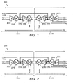
- FIG. 1 is a block diagram of an example circuit that can provide IM2 compensation signals that may be used in a distortion compensation circuit.
- Circuit 100 includes in phase inputs I (i.e., IP2 A2 /IM2 A2 and IP2 A3 /IM2 A3 ) and quadrature inputs Q (i.e., QP2 A3 /QM2 A3 and QP2 A2 /QM2 A2 ), where the I inputs (IP2 A2 /IM2 A2 and IP2 A3 /IM2 A3 ) and Q inputs (QP2 A3 /QM2 A3 and QP2 A2 /QM2 A2 ) may be attenuated (e.g., by use of a voltage attenuator) versions of the I and Q inputs, respectively.
- I i.e., IP2 A2 /IM2 A2 and IP2 A3 /IM2 A3
- Q Q inputs
- the I side of circuit 100 includes a transconductance block 102a, a multiplier 104a, a fold circuit 106a, and an output multiplier 108a.
- the multiplier 104a multiplies the two input I signals, providing at its output the I 2 term in equation 1.
- the multiplier 104b multiplies the two Q signals, providing the Q 2 of equation 1.
- the I 2 term and the Q 2 are summed by the folding circuit 108a for the I side, and the folding circuit 108b for the Q side, thereby providing the second order intermodulation correction signal of equation 1.
- the output signals of the I side and Q side may be scaled independently by multipliers 108a and 108b, based on inputs V IM2I and V IM2Q , respectively.
- V IM2I and V IM2Q are differential DC control voltages that can be generated by passing a differential control current through diodes as shown in Fig. 12 .
- the V IM2I and V IM2Q components can be adjusted independently to obtain the optimal amount and polarity of IM2 distortion to cancel the IM2 distortion present in the original I or Q signal paths.
- the determination of the optimal amount of distortion is performed by a calibration step for the IQ signal path, wherein the IM2 component generated by a 2-tone test signal of the form shown in Eq. A1 and A2 is measured in the analog or digital domain using a measuring receiver capable of frequency selectively measuring the IM2 tone power present at the IM2 distortion frequency. Optimization algorithms could be applied to iteratively measure and reduce the IM2 level by calculating an updated control current value at each iteration.
- FIG. 2 is a block diagram of an example circuit that can provide HD2 compensation signals at 0° that may be used in a distortion compensation circuit.
- the inputs and components of circuit 200 are substantially similar to those of circuit 100, and will therefore not be repeated here for brevity.
- the multiplier 204a multiplies the two input I signals, providing the I 2 term of equation 2.
- the multiplier 204b multiplies the two Q signals, providing the Q 2 of equation 2. Since the I 2 term and the Q 2 are coupled to the inverse polarities of folding circuits 206a and 206b, each folding circuit 108a/108b subtracts the I 2 and Q 2 signals from each other for the I side and Q side, respectively.
- the output signals of the I side and Q side may be scaled independently by multipliers 208a and 208b, based on inputs V HD2IX and V HD2QX , respectively.
- FIG. 3 is a block diagram of an example circuit that can provide HD2 compensation signals at 90° that may be used in a distortion compensation circuit.
- the inputs and components of circuit 300 are substantially similar to those of circuits 100 and 200, and will therefore not be repeated here for brevity.
- the multiplier 304a multiplies the input I signal by the input Q signal, providing an IQ term.
- multiplier 304b multiplies the input Q signal with the input I signal, providing another IQ term. Both IQ terms are summed by the folding circuits 306a and 306b, respectively, thereby providing the 2IQ term of equation 3.
- the output signals of the I side and Q side may be scaled independently by multipliers 308a and 308b, based on inputs V HD2IY and V HD2QY , respectively.
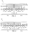
- FIG. 4 is a block diagram of an example circuit that can provide IM3 compensation signals at 0° that may be used in a distortion compensation circuit.
- Circuit 400 includes in phase inputs I (i.e., IP2 A2 /IM2 A2 , IP2 A3 /IM2 A3 , and IP2 A1 /IM2 A1 ) and quadrature inputs Q (i.e., QP2 A3 /QM2 A3 and QP2 A2 /QM2 A2 ).
- the I side of circuit 400 includes a transconductance block 402a, a first multiplier 404a, a second multiplier 406a, a fold circuit 408a, and an output multiplier 410a.
- the first multiplier 404a provides an I 2 output, which is multiplied by another I by the second multiplier 406a, thereby providing the I 3 component of equation 4.
- the output of the first multiplier 404b provides the Q 2 component.
- the second multiplier on the Q side 406b multiplies the Q 2 component by I, thereby providing the Q 2 I component of equation 4.
- the I 3 and the Q 2 I components are summed together by the folding circuits 408a and 408b, respectively, thereby providing the third order intermodulation correction signal of equation 4.
- the output signals of the I side and Q side may be scaled independently by multipliers 410a and 410b, based on inputs V IM3IX and V IM3QX , respectively.
- FIG. 5 is a block diagram of an example circuit that can provide IM3 compensation signals at 90° that may be used in a distortion compensation circuit.
- Circuit 500 includes in phase inputs I (i.e., IP2 A2 /IM2 A2 , and IP2 A3 /IM2 A3 ) and quadrature inputs Q (i.e., QP2 A3 /QM2 A3 , QP2 A2 /QM2 A2 , and QP2 A1 /QM2 A1 .
- the components of the circuit 500 are substantially similar to those of circuit 400, and will therefore not be repeated here for brevity.
- the first multiplier 504b provides a Q 2 output, which is multiplied by another Q by the second multiplier 506b, thereby providing the Q 3 component of equation 5.
- the output of the first multiplier 504a provides the I 2 component.
- the second multiplier on the I side 506a multiplies the I 2 component by Q, thereby providing the I 2 Q component of equation 5.
- the Q 3 and the I 2 Q components are summed together by the folding circuits 508a and 508b, respectively, thereby providing the third order intermodulation correction signal of equation 5.
- the output signals of the I side and Q side may be scaled independently by multipliers 510a and 510b, based on inputs V IM3IY and U IM3QY , respectively.
- FIG. 6 is a block diagram of an example circuit that can provide HD3 compensation signals at 0° that may be used in a distortion compensation circuit.
- Circuit 600 includes in phase inputs I (i.e., IP2 A2 /IM2 A2 , IP2 A3 /IM2 A3 , IP2 A1 /IM2 A1 , and IP1 A1 /IM1 A1 ) and quadrature inputs Q (i.e., QP1 A3 /QM1 A3 and QP1 A2 /QM1 A2 ).
- I i.e., IP2 A2 /IM2 A2
- IP2 A3 /IM2 A3 IP2 A1 /IM2 A1
- IP1 A1 /IM2 A1 IP1 A1 /IM1 A1
- Q quadrature inputs
- the components of the circuit 600 are substantially similar to those of circuits 400 and 500, and will therefore not be repeated here for brevity.
- the first multiplier 604a provides an I 2 output, which is multiplied by another I by the second multiplier 606a, thereby providing the I 3 component of equation 6.
- the output signals of the I side and Q side may be scaled independently by multipliers 610a and 610b, based on inputs V HD3IX and V HD3QX , respectively.
- the attenuator connections such as M1 or P1 are 3 ⁇ (1/3) larger in magnitude than the M2 or P2 signals, so that a signal like IM1A1 is 3 A (1/3) times greater than IM2A1.
- FIG. 7 is a block diagram of an example circuit that can provide HD3 compensation signals at 90° that may be used in a distortion compensation circuit.
- Circuit 700 includes in phase inputs I (i.e., IP1 A2 /IM1 A2 , and IP1 A3 /IM1 A3 ) and quadrature inputs Q (i.e., QP2 A3 /QM2 A3 , QP2 A2 /QM2 A2 , QP2 A1 /QM2 A1 , and QP1 A1 /QM1 A1 ).
- the components of the circuit 700 are substantially similar to those of circuit 600, and will therefore not be repeated here for brevity.
- the first multiplier 704b provides a Q 2 output, which is multiplied by another I by the second multiplier 706b, thereby providing the Q 3 component of equation 7.
- the quadrature Q attenuator attenuates the baseband quadrature Q signal such that it is greater than the attenuated baseband quadrature Q signal by a factor of 3 ⁇ (1/3).
- circuit 700 is substantially similar to circuit 600, except that the circuit has been flipped between the I side and Q side.
- FIGS. 1 to 7 show block level schematics of an example implementation of each of the equations 1-7, respectively.
- the blocks named "g m " may each be transconductance amplifiers, such as the one discussed later in the context of in FIG.9b .
- the blocks marked with an X may each be multipliers, such as the one discussed in more detail later in the context of FIG. 10b .
- the blocks named "FOLD" may each be current folds, such as the one discussed in more detail in the context of FIG. 8b .
- FIG. 8a is a symbol of a current fold block and FIG. 8b is an example schematic diagram of the symbol of FIG. 8a .
- Circuit 800 illustrates, by way of example, a circuit that may be used as the current fold block illustrated in FIGS. 1 to 7 .
- Circuit 800 includes a left side and a right side, which are mutually similar. The two halves can be viewed as single-ended circuits that have been mated together to form a differential configuration. Accordingly, resistor R1 (804a), transistor Q1 (806a), and current source I1 (808a) may be matched by R2 (804b), Q2 (806b), and I2 (808b), respectively.
- a differential current impressed on nodes I INP and I INM may be folded and output through nodes I OUTP and I OUTM .
- the current provided at output node IOUTP is substantially similar to the current at the emitter of transistor Q1 (806a). The same is true on the right side of the circuit 800.
- Voltage bias point V BFOLD may be set so that the common mode voltage of the input nodes (i.e., I INP and I INM ) does not cause the preceding transistors (i.e., Q1 and Q2, respectively) to saturate.
- resistors R1/R2 may be configured to provide about a 500mV drop from the positive rail 810 (which may be Vcc for bipolar, Vdd for FET, or any other suitable voltage). Accordingly, the voltage at the common node V BFOLD may be about 1.2V below the positive rail 810, due to the diode voltage drop from transistors Q1 and Q2, respectively.
- FIG. 9a is a symbol of a transconductance amplifier and FIG. 9b is a schematic diagram of an example differential pair of transistors that may be used as the transconductance amplifier illustrated in FIGS. 1 to 7 .
- two transistors 904a and 904b share a common node at each emitter, respectively, which is coupled to a current source 906.
- the transconductance g m may be equal to I1/(2V T ), where V T is the transistor thermal voltage.
- FIG. 10a is a symbol of a multiplier and FIG. 10b is a schematic diagram of an example multiplier that may be used as the multiplier illustrated in FIGS. 1 to 7 .
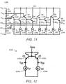
- FIG. 11 is a schematic diagram of an example input attenuator and voltage buffer circuit, which is sometimes referred to herein as an "attenuator.”
- Circuit 1100 may be used, for example, to attenuate the baseband in-phase I signal of a distortion compensation circuit. It may also be used to attenuate the baseband quadrature signal. An example application will be illustrated later in the context of FIG. 13 .
- Circuit 1100 includes resistors R1 (1102), R2 (1104), R3 (1106), R4 (1108), and R5 (1110) connected in series. Circuit 1100 also includes transistors Q1 (1120), Q2 (1122), Q3 (1124), Q4 (1126), Q5 (1128), Q6 (1130), Q7 (1132), and Q8 (1134), which are each configured as emitter followers, having each emitter coupled to a corresponding current source (i.e., I1 (1140) to I8 (1154), respectively).
- the resistance pairs R1 / R5 and R2 / R4 match.
- the values of the resistances may be adjusted such that the voltage signal at the P1, M1 nodes is 3 ⁇ 3 times larger than the voltage signal at the P2, M2 nodes.
- the attenuator factor 3 ⁇ 3 may be chosen in order to implement the factor 3 in equations 6 and 7, since three signals are being multiplied together.
- resistances R2 and R4 are set to be 0.2211 times the value of R3 to obtain this 3 ⁇ 3 factor.
- Resistances R1 and R5 may be set to control the amount of signal attenuation for a desired range of distortion to be generated by the distortion compensation sub-blocks.
- Matched transistors Q1 to Q8 along with their associated current sources may be voltage buffers used for level shifting of the voltage signals from the attenuator to suitable bias points for the operation of the compensation circuits.
- FIG. 12 is a schematic diagram of an example circuit that may be used to transform control currents into control voltages.
- Circuit 1200 includes a left half and a right half that are mutually similar. The two halves can be viewed as single-ended circuits that have been mated together to form a differential configuration of current to voltage circuit.
- FIG. 13 is a block diagram of an example distortion compensation circuit.
- Distortion compensation circuit 1300 includes an in-phase I attenuator 1302 that is configured to attenuate the baseband in-phase I signal. There is an in-phase Q attenuator 1304 configured to attenuate the baseband Q signal.
- the I signal comprises differential signals IP and IM and the Q signal comprises differential signals QP and QM.
- the attenuators were described by way of example in the context of the discussion of FIG. 11 .
- circuit 1300 may include one or more of the circuits that are represented by blocks 1310 to 1322, which are configured to receive the attenuated in-phase I signal and the attenuated baseband Q signal.
- Each of the circuits 1310 to 1322 is configured to implement the functions of equations 1 to 7 above, respectively.
- the distortion compensation circuit 1300 is configured to use the result of at least one of the calculation circuits 1310 to 1322 to generate an I distortion compensation signal (represented by differential signals IP/IM) at a first output, and a Q distortion compensation signal (represented by differential signals QP/QM) at a second output.
- I distortion compensation signal represented by differential signals IP/IM
- QP/QM differential signals
- FIG. 14 is a block diagram illustrating use of a distortion compensation circuit 1402 to linearize a demodulation circuit 1400.
- the distortion compensation block 1402 is the circuit illustrated in FIG. 13 .
- Each R LOAD i.e., 1410a/b and 1412a/b
- Each circled “X” may be a multiplier circuit (e.g., 1420a and 1420b), such as the one illustrated in FIG. 10b .
- Each transconductance unit e.g., 1430a and 1430b
- FIG. 15 is a block diagram illustrating use of a distortion compensation circuit 1502 to linearize an amplifier 1500.
- the distortion compensation block 1502 is the circuit illustrated in FIG. 13 .
- the amplifier 1500 comprises amplifiers 1530a and 1530b that may each be differential linear amplifiers.
- Each R LOAD i.e., 1510a/b and 1512a/b
- Each R LOAD may be a load resistor.
- FIG. 16 is a graph of typical distortion vs a differential control current I CD .
- the control current I CD may be better understood in view of FIG. 12 , where I CD represents the differential current between V CP and V CM .
- FIG.16 illustrates a typical response of one of the distortion components (e.g., IM2, HD2, IM3, and HD3), versus a corresponding differential control current I CD as in FIG.12 . Accordingly, FIG. 16 illustrates that, at a calculated ICD, there is a spot where the distortion is reduced most effectively.
- the distortion components e.g., IM2, HD2, IM3, and HD3
- any signal discussed herein may be scaled, buffered, scaled and buffered, converted to another mode (e.g., voltage, current, charge, time, etc.,), or converted to another state (e.g., from HIGH to LOW and LOW to HIGH) without materially changing the underlying control method.
- higher order distortion products could be compensated for by using this same method.
- the use of more multipliers and/or different attenuation factors could be used to calculate the result of more complicated equations for higher order distortions such as IM5 HD4 HD5, etc.
- the NPN transistors in FIGS. 9 to 12 could be replaced by NMOS transistors, and the PNP transistors of FIG. 8 could be replaced with PMOS transistors.
- the circuits could be reconfigured to use PNP transistors instead of NPN transistors (and PMOS transistors instead of NMOS) while still adhering to the principles of the subject matter disclosed herein.
- the circuits shown in FIGS. 8 to 10 could have their basic function implemented or improved in numerous ways.
- the transconductor of FIG. 9 could be made more linear by using an emitter degeneration resistance. This may be desirable if the input signals were larger because less attenuation was chosen.
- a pre-distortion circuit such as that illustrated by FIG.12 could be used at the multiplier inputs from the attenuator in order to obtain a more linear response for larger input signals.
Landscapes
- Engineering & Computer Science (AREA)
- Power Engineering (AREA)
- Computer Networks & Wireless Communication (AREA)
- Signal Processing (AREA)
- Physics & Mathematics (AREA)
- Nonlinear Science (AREA)
- Amplifiers (AREA)
Applications Claiming Priority (3)
| Application Number | Priority Date | Filing Date | Title |
|---|---|---|---|
| US201562120711P | 2015-02-25 | 2015-02-25 | |
| US201562134389P | 2015-03-17 | 2015-03-17 | |
| US14/806,492 US9660856B2 (en) | 2015-02-25 | 2015-07-22 | Distortion compensation circuit |
Publications (2)
| Publication Number | Publication Date |
|---|---|
| EP3062437A2 true EP3062437A2 (de) | 2016-08-31 |
| EP3062437A3 EP3062437A3 (de) | 2016-11-16 |
Family
ID=55405089
Family Applications (1)
| Application Number | Title | Priority Date | Filing Date |
|---|---|---|---|
| EP16000320.8A Withdrawn EP3062437A3 (de) | 2015-02-25 | 2016-02-09 | Verzerrungskompensationsschaltung |
Country Status (5)
| Country | Link |
|---|---|
| US (1) | US9660856B2 (de) |
| EP (1) | EP3062437A3 (de) |
| KR (1) | KR20160103942A (de) |
| CN (1) | CN105915185B (de) |
| TW (1) | TW201635766A (de) |
Families Citing this family (1)
| Publication number | Priority date | Publication date | Assignee | Title |
|---|---|---|---|---|
| TWI677192B (zh) * | 2018-11-05 | 2019-11-11 | 瑞昱半導體股份有限公司 | 諧波補償裝置 |
Citations (4)
| Publication number | Priority date | Publication date | Assignee | Title |
|---|---|---|---|---|
| US7876867B2 (en) | 2006-08-08 | 2011-01-25 | Qualcomm Incorporated | Intermodulation distortion detection and mitigation |
| US8050649B2 (en) | 2005-08-30 | 2011-11-01 | Qualcomm Incorporated | Downconversion mixer with IM2 cancellation |
| US8483646B2 (en) | 2011-12-12 | 2013-07-09 | Linear Technology Corporation | Second order intermodulation canceller |
| US8848824B2 (en) | 2008-03-07 | 2014-09-30 | Andrew M. Teetzel | High efficiency RF system linearizer using controlled complex nonlinear distortion generators |
Family Cites Families (8)
| Publication number | Priority date | Publication date | Assignee | Title |
|---|---|---|---|---|
| JP4394409B2 (ja) | 2003-09-25 | 2010-01-06 | 株式会社日立国際電気 | プリディストーション方式歪補償機能付き増幅器 |
| US7430248B2 (en) * | 2004-01-27 | 2008-09-30 | Crestcom, Inc. | Predistortion circuit and method for compensating nonlinear distortion in a digital RF communications transmitter |
| US7469491B2 (en) | 2004-01-27 | 2008-12-30 | Crestcom, Inc. | Transmitter predistortion circuit and method therefor |
| JP4557702B2 (ja) * | 2004-12-17 | 2010-10-06 | 株式会社東芝 | 受信機 |
| DE602006000525T2 (de) * | 2005-06-03 | 2009-02-05 | Ntt Docomo Inc. | Mehrbandvorverzerrer mit Korrekturwertetabellen |
| JP2008022111A (ja) | 2006-07-11 | 2008-01-31 | Sony Corp | 歪み補償装置、及び無線通信装置 |
| US7804922B2 (en) * | 2007-03-02 | 2010-09-28 | Skyworks Solutions, Inc. | System and method for adjacent channel power detection and dynamic bandwidth filter control |
| EP2876852A1 (de) * | 2013-11-22 | 2015-05-27 | Sequans Communications Limited | Senderlinearisierung |
-
2015
- 2015-07-22 US US14/806,492 patent/US9660856B2/en active Active
-
2016
- 2016-02-09 EP EP16000320.8A patent/EP3062437A3/de not_active Withdrawn
- 2016-02-22 TW TW105105148A patent/TW201635766A/zh unknown
- 2016-02-24 KR KR1020160021789A patent/KR20160103942A/ko not_active Withdrawn
- 2016-02-25 CN CN201610104467.XA patent/CN105915185B/zh active Active
Patent Citations (4)
| Publication number | Priority date | Publication date | Assignee | Title |
|---|---|---|---|---|
| US8050649B2 (en) | 2005-08-30 | 2011-11-01 | Qualcomm Incorporated | Downconversion mixer with IM2 cancellation |
| US7876867B2 (en) | 2006-08-08 | 2011-01-25 | Qualcomm Incorporated | Intermodulation distortion detection and mitigation |
| US8848824B2 (en) | 2008-03-07 | 2014-09-30 | Andrew M. Teetzel | High efficiency RF system linearizer using controlled complex nonlinear distortion generators |
| US8483646B2 (en) | 2011-12-12 | 2013-07-09 | Linear Technology Corporation | Second order intermodulation canceller |
Also Published As
| Publication number | Publication date |
|---|---|
| EP3062437A3 (de) | 2016-11-16 |
| US20160248617A1 (en) | 2016-08-25 |
| CN105915185A (zh) | 2016-08-31 |
| KR20160103942A (ko) | 2016-09-02 |
| TW201635766A (zh) | 2016-10-01 |
| CN105915185B (zh) | 2019-06-28 |
| US9660856B2 (en) | 2017-05-23 |
Similar Documents
| Publication | Publication Date | Title |
|---|---|---|
| US6794938B2 (en) | Method and apparatus for cancellation of third order intermodulation distortion and other nonlinearities | |
| CN107078980B (zh) | 一种模拟预失真器核心模块及模拟预失真器系统 | |
| WO2009030938A2 (en) | Multiplier, mixer, modulator, receiver and transmitter | |
| US6529075B2 (en) | Amplifier with suppression of harmonics | |
| US20070037544A1 (en) | Integrated RF circuits | |
| JPH06177668A (ja) | シングルエンド入力を差動出力に変換する増幅回路の出力の平衡を向上させるための回路および方法 | |
| TW202107838A (zh) | 具有雜訊消除之寬帶低雜訊放大器 | |
| EP3062437A2 (de) | Verzerrungskompensationsschaltung | |
| CN104734641A (zh) | 混频器 | |
| JP2002057533A (ja) | 前置歪み補償回路、低歪み電力増幅器、及びその制御方法 | |
| JP2010220195A (ja) | カレントコンベアベースの計器増幅器 | |
| EP2605402B1 (de) | Intermodulationsabbruch dritter Ordnung für RF-Transleiter | |
| US7750734B2 (en) | Apparatus and methods for amplifiers | |
| JP5104561B2 (ja) | 直交信号出力回路 | |
| EP3062438A1 (de) | Phasenfehlerausgleichsschaltung | |
| US9641127B1 (en) | Operational transconductance amplifier of improved linearity | |
| JP3510806B2 (ja) | 周波数変換回路及び高周波無線通信装置 | |
| JP2012100224A (ja) | 広帯域増幅器 | |
| EP3955459B1 (de) | Verstärkerschaltung, empfängerschaltung und verfahren zur verwendung der verstärkerschaltung | |
| CN111682855B (zh) | 信号处理装置 | |
| US9124215B2 (en) | Mixer circuit | |
| Kuremyr | A Study on Linearity of Mixers for Homodyne Receivers | |
| WO2006006239A1 (ja) | 移相回路及び位相補正方法 | |
| Wu et al. | Design of differential amplifier with negative impedance compensation | |
| CN105071779A (zh) | 一种预失真器和一种信号接收机 |
Legal Events
| Date | Code | Title | Description |
|---|---|---|---|
| PUAI | Public reference made under article 153(3) epc to a published international application that has entered the european phase |
Free format text: ORIGINAL CODE: 0009012 |
|
| AK | Designated contracting states |
Kind code of ref document: A2 Designated state(s): AL AT BE BG CH CY CZ DE DK EE ES FI FR GB GR HR HU IE IS IT LI LT LU LV MC MK MT NL NO PL PT RO RS SE SI SK SM TR |
|
| AX | Request for extension of the european patent |
Extension state: BA ME |
|
| PUAL | Search report despatched |
Free format text: ORIGINAL CODE: 0009013 |
|
| AK | Designated contracting states |
Kind code of ref document: A3 Designated state(s): AL AT BE BG CH CY CZ DE DK EE ES FI FR GB GR HR HU IE IS IT LI LT LU LV MC MK MT NL NO PL PT RO RS SE SI SK SM TR |
|
| AX | Request for extension of the european patent |
Extension state: BA ME |
|
| RIC1 | Information provided on ipc code assigned before grant |
Ipc: H03D 3/00 20060101AFI20161011BHEP Ipc: H03F 1/32 20060101ALI20161011BHEP |
|
| 17P | Request for examination filed |
Effective date: 20170515 |
|
| RBV | Designated contracting states (corrected) |
Designated state(s): AL AT BE BG CH CY CZ DE DK EE ES FI FR GB GR HR HU IE IS IT LI LT LU LV MC MK MT NL NO PL PT RO RS SE SI SK SM TR |
|
| 17Q | First examination report despatched |
Effective date: 20170727 |
|
| GRAP | Despatch of communication of intention to grant a patent |
Free format text: ORIGINAL CODE: EPIDOSNIGR1 |
|
| RIC1 | Information provided on ipc code assigned before grant |
Ipc: H03D 3/00 20060101AFI20180417BHEP Ipc: H04L 27/36 20060101ALI20180417BHEP Ipc: H04B 1/10 20060101ALI20180417BHEP Ipc: H03F 1/32 20060101ALI20180417BHEP Ipc: H04B 3/32 20060101ALI20180417BHEP Ipc: H04L 25/03 20060101ALI20180417BHEP Ipc: H03F 3/45 20060101ALI20180417BHEP |
|
| INTG | Intention to grant announced |
Effective date: 20180507 |
|
| STAA | Information on the status of an ep patent application or granted ep patent |
Free format text: STATUS: THE APPLICATION IS DEEMED TO BE WITHDRAWN |
|
| 18D | Application deemed to be withdrawn |
Effective date: 20180918 |