EP3057100B1 - Speichervorrichtung und betriebsverfahren dafür - Google Patents
Speichervorrichtung und betriebsverfahren dafür Download PDFInfo
- Publication number
- EP3057100B1 EP3057100B1 EP15168965.0A EP15168965A EP3057100B1 EP 3057100 B1 EP3057100 B1 EP 3057100B1 EP 15168965 A EP15168965 A EP 15168965A EP 3057100 B1 EP3057100 B1 EP 3057100B1
- Authority
- EP
- European Patent Office
- Prior art keywords
- access mode
- command code
- logic unit
- program
- array
- Prior art date
- Legal status (The legal status is an assumption and is not a legal conclusion. Google has not performed a legal analysis and makes no representation as to the accuracy of the status listed.)
- Active
Links
- 238000011017 operating method Methods 0.000 title 1
- 238000003491 array Methods 0.000 claims description 24
- 238000000034 method Methods 0.000 claims description 13
- 230000003287 optical effect Effects 0.000 description 2
- 230000003068 static effect Effects 0.000 description 1
Images


Classifications
-
- G—PHYSICS
- G11—INFORMATION STORAGE
- G11C—STATIC STORES
- G11C7/00—Arrangements for writing information into, or reading information out from, a digital store
-
- G—PHYSICS
- G06—COMPUTING; CALCULATING OR COUNTING
- G06F—ELECTRIC DIGITAL DATA PROCESSING
- G06F12/00—Accessing, addressing or allocating within memory systems or architectures
- G06F12/02—Addressing or allocation; Relocation
- G06F12/0223—User address space allocation, e.g. contiguous or non contiguous base addressing
- G06F12/023—Free address space management
- G06F12/0238—Memory management in non-volatile memory, e.g. resistive RAM or ferroelectric memory
- G06F12/0246—Memory management in non-volatile memory, e.g. resistive RAM or ferroelectric memory in block erasable memory, e.g. flash memory
-
- G—PHYSICS
- G11—INFORMATION STORAGE
- G11C—STATIC STORES
- G11C16/00—Erasable programmable read-only memories
- G11C16/02—Erasable programmable read-only memories electrically programmable
- G11C16/06—Auxiliary circuits, e.g. for writing into memory
-
- G—PHYSICS
- G11—INFORMATION STORAGE
- G11C—STATIC STORES
- G11C7/00—Arrangements for writing information into, or reading information out from, a digital store
- G11C7/10—Input/output [I/O] data interface arrangements, e.g. I/O data control circuits, I/O data buffers
- G11C7/1015—Read-write modes for single port memories, i.e. having either a random port or a serial port
- G11C7/1045—Read-write mode select circuits
-
- G—PHYSICS
- G06—COMPUTING; CALCULATING OR COUNTING
- G06F—ELECTRIC DIGITAL DATA PROCESSING
- G06F2212/00—Indexing scheme relating to accessing, addressing or allocation within memory systems or architectures
- G06F2212/10—Providing a specific technical effect
- G06F2212/1041—Resource optimization
- G06F2212/1044—Space efficiency improvement
-
- G—PHYSICS
- G06—COMPUTING; CALCULATING OR COUNTING
- G06F—ELECTRIC DIGITAL DATA PROCESSING
- G06F2212/00—Indexing scheme relating to accessing, addressing or allocation within memory systems or architectures
- G06F2212/10—Providing a specific technical effect
- G06F2212/1048—Scalability
-
- G—PHYSICS
- G06—COMPUTING; CALCULATING OR COUNTING
- G06F—ELECTRIC DIGITAL DATA PROCESSING
- G06F2212/00—Indexing scheme relating to accessing, addressing or allocation within memory systems or architectures
- G06F2212/72—Details relating to flash memory management
- G06F2212/7204—Capacity control, e.g. partitioning, end-of-life degradation
Definitions
- the present disclosure relates to a memory device and operation method of the same and, more particularly, to a memory device having extra arrays of reconfigurable size.
- a memory device may include a plurality of pages for storing user data, and the size of the pages is fixed and unchangeable. However, in some applications, it is desirable to store extra data in the memory device.
- US 2011/0258368 A1 concerns a memory system including a non-volatile memory device including a plurality of pages and a controller connected electrically with the non-volatile memory device and configured to control the non-volatile memory device.
- the non-volatile memory device is configured to be capable of storing data from a set number of write operations before data erasing with respect to each page.
- the controller is configured to divide each page of the non-volatile memory device into first and second areas, to perform a write operation of the first area by the NOP, and to write an invalidation mark in the second area.
- EP 1 632 950 A1 concerns a non-volatile memory device that can reduce the time required for the initialization process.
- the non-volatile memory device includes a non-volatile memory array having a plurality of pages. Each page includes a plurality of non-volatile memory cells, a first region for storing data, and a second region for storing control data that is associated with the data of the first region.
- the non-volatile memory device further includes a read out unit for reading out data from the pages, and a data buffer for temporarily storing data that has been read out from the pages by the read out unit. When reading out the control data, the read out unit reads out the second regions, across a plurality of pages, at one time.
- US 2014/0181378 A1 concerns a control device including, a reading and writing control unit configured to control writing and reading of data on and from a non-volatile memory that has a plurality of blocks each set to be a unit for performing erasure of data.
- the non-volatile memory stores order information indicating an order of the blocks in which data is to be written.
- the reading and writing control unit selects a writing target block that is a target block for writing of data according to the order indicated by the order information, and writes data in the selected writing target block.
- a memory device includes the features of claim 1.
- a memory device includes the features of claim 10.
- a method of operating a memory device includes a plurality of array blocks for storing array data and a plurality of extra array blocks respectively corresponding to the plurality of array blocks for storing extra data.
- the method includes receiving a read instruction including a read command code, and determining whether the read command code is a first read command code or a second read command code. If the read command code is determined to be the first read command code, the method includes sequentially reading out the array data stored in the plurality of pages. If the read command code is determined to be the second read command code, the method includes sequentially reading out the array data stored in the plurality of pages and the extra data stored in the plurality of extra arrays.
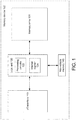
- FIG. 1 schematically illustrates a memory device 100 having extra arrays of reconfigurable size, according to an illustrated embodiment.
- Memory device 100 includes an input/output (I/O) interface 110, a logic unit 120 communicatively coupled to I/O interface 110, a memory array 130 communicatively coupled to logic unit 120, and a non-volatile memory 140 communicatively coupled to logic unit 120.
- I/O interface 110 includes a plurality of pins (not shown) coupled to an external circuit (not shown). I/O interface 110 receives various instructions and data to be programmed, i.e., written, into memory array 130 from the external circuit. I/O interface 110 also outputs data read from memory array 130 to the external circuit.
- Logic unit 120 receives the instructions and the data from I/O interface 110, and performs various operations (e.g., read, program, erase, etc.) on memory array 130 according to the received instructions.
- Logic unit 120 includes processing circuitry 122 and an internal register 124.
- Processing circuitry 122 includes logic circuits that control the overall operation of logic unit 120.
- Internal register 124 stores temporary data used by processing circuitry 122.
- Internal register 124 can be implemented by a volatile memory, such as a static random-access memory (SRAM), a random-access memory (RAM), and a dynamic random-access memory (DRAM).
- Non-volatile memory 140 stores permanent data used by processing circuitry 122.
- Non-volatile memory 140 also stores information about chip configuration for memory device 100.
- Non-volatile memory 140 can be implemented by a flash memory, a read-only memory (ROM), a ferroelectric random-access memory (F-RAM), a magnetic computer storage device, or an optical disc.
- Memory array 130 is a non-volatile memory such as a flash memory, a read-only memory (ROM), a ferroelectric random-access memory (F-RAM), a magnetic computer storage device, or an optical disc.
- internal register 124 of logic unit 120 stores a plurality of command codes and their corresponding operations.
- processing circuitry 122 of logic unit 120 parses the instruction to identify a command code, compares the identified command code with the plurality of command codes stored in internal register 124 to look for an operation corresponding to the identified command code, and then performs the operation.
- FIG. 2 schematically illustrates an array structure of memory array 130, according to an illustrated embodiment.
- Memory array 130 includes a plurality of array blocks 200 and a plurality of extra array blocks 210.
- Each extra array block 210 corresponds to one of the plurality of array blocks 200. That is, extra array block 0 corresponds to array block 0, extra array block 1 corresponds to array block 1,..., and extra array block n corresponds to array block n.
- Each array block 200 includes a plurality of, e.g., eight (8), pages 220.
- Each extra array block 210 includes a plurality of, e.g., eight (8), extra arrays 230.
- Each extra array 230 corresponds to one of the plurality of pages 220.
- extra array 0 corresponds to page 0
- extra array 1 corresponds to page 1
- extra array 7 corresponds to page 7.
- Each page 220 has a fixed size of, e.g., 256 bytes.
- Each extra array 230 has a reconfigurable size of, e.g., 1 byte, 2 bytes, or 8 bytes, etc.
- the plurality of pages 220 are used to store the array data defined by the user.
- the plurality of extra arrays 230 are used to store extra data associated with the array data stored in the corresponding pages 220.
- the extra data stored in extra array 0 includes Error Checking and Correcting (ECC) code, and/or security content, etc., associated with the array data stored in page 0.
- ECC Error Checking and Correcting
- the array structure illustrated in FIG. 2 is a logical array structure of memory array 130 usable by the external circuit.
- the address of data in the logical array structure (referred to as "logical address”) can be mapped to the address of data in a physical array structure (referred to as "physical address") by scramble transfer.
- logical address the address of data in the logical array structure
- physical address the address of data in a physical array structure
- the logical array structure of memory array 130 includes extra arrays 230 of reconfigurable size
- the physical array structure of memory array 130 also can be remapped by scramble transfer to include such extra arrays 230.
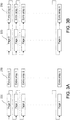
- FIG. 3A schematically illustrates an access sequence of memory array 130, according to a first access mode of an illustrated embodiment.
- the first access mode only pages 220 are accessed sequentially in the order of page 0, page 1, page 2,..., page n. Extra arrays 230 are not accessed.
- the first access mode can be applied when the extra data stored in extra arrays 230 includes security content associated with the array data stored in pages 220.
- FIG. 3B schematically illustrates another access sequence of memory array 130, according to a second access mode of an illustrated embodiment.
- both of pages 220 and extra arrays 230 are accessed sequentially in the order of page 0, extra array 0, page 1, extra array 1, page 2, extra array 2,..., page n, extra array n.
- logic unit 120 of memory device 100 can receive a read instruction that includes access information related to whether to perform a memory access operation in the first access mode or the second access mode.
- logic unit 120 sequentially reads out the array data stored in pages 220 in the order of page 0, page 1, page 2,..., page n.
- the extra data stored in extra arrays 230 are excluded from the read out sequence. That is, the extra data stored in extra arrays 230 are not read out.
- logic unit 120 When logic unit 120 performs a read operation in the second access mode, logic unit 120 sequentially reads out both the array data stored in pages 220 and the extra data stored in extra arrays in the order of page 0, extra array 0, page 1, extra array 1, page 2, extra array 2,..., page n, extra array n.
- FIG. 4 schematically illustrates a read instruction 400 for performing a read operation, according to an illustrated embodiment.
- Read instruction 400 is issued to logic unit 120 in order to read data stored in memory array 130.
- read instruction 400 includes a total of four (4) bytes, i.e., a first (1st) byte, a second (2nd) byte, a third (3rd) byte, and a fourth (4th) byte.
- the first (1st) byte includes a read command code, which can be pre-defined to instruct logic unit 120 to perform the read operation in the first access mode or in the second access mode, and, if in the second access mode, specify the size of each extra array 230.
- the second (2nd) byte includes a first address segment AD1, which includes address bits A23 to A16.
- the third (3rd) byte includes a second address segment AD2, which includes address bits A15 to A8.
- the fourth (4th) byte includes a third address segment AD3, which includes address bits A7 to A0.
- the address segments AD1, AD2, and AD3 constitute a 24-bit address, which represents a starting address in memory array 130 for the read operation.
- a read command code of 03 in hexadecimal hereinafter referred to as "03(hex)" can be pre-defined to instruct logic unit 120 to perform a read operation in the first access mode.
- logic unit 120 When logic unit 120 receives an instruction including 03(hex) followed by a 24-bit address, logic unit 120 performs a read operation in the first access mode as illustrated in FIG. 3A , sequentially reading out the array data stored in pages 220 of memory array 130, starting from a location having the 24-bit address.
- a read command code of 66(hex) can be pre-defined to instruct logic unit 120 to perform a read operation in the second access mode, and to specify that the size of each extra array 230 is 2 bytes.
- logic unit 120 When logic unit 120 receives an instruction including 66(hex) followed by a 24-bit address, logic unit 120 performs a read operation according to the second access mode as illustrated in FIG.
- a read command code of 68(hex) can be pre-defined to instruct logic unit 120 to perform a read operation in the second access mode, and to specify that the size of each extra array 230 is 4 bytes.
- logic unit 120 receives an instruction including 68(hex) followed by a 24-bit address
- logic unit 120 performs a read operation according to the second access mode as illustrated in FIG. 3B , sequentially reading out both the array data stored in pages 220 of memory array 130 and the extra data stored in the 4 bytes of each of extra arrays 230 of memory array 130, starting from a location having the 24-bit address.
- FIG. 5 schematically illustrates a fast read instruction 500 for performing a fast read operation, according to an illustrated embodiment.
- Fast read instruction 500 is issued to logic unit 120 in order to quickly read the data stored in memory array 130.
- fast read instruction 500 additionally includes a fifth (5th) byte, which is a dummy byte.
- the dummy byte provides an extra time margin required for sensing data.
- the read command code in the first byte can be pre-defined to instruct logic unit 120 to perform a fast read operation in the first access mode or the second access mode, and the size of each extra array 230.
- a read command code of 0B(hex) can be pre-defined to instruct logic unit 120 to perform a fast read operation in the first access mode.
- logic unit 120 When logic unit 120 receives an instruction including 0B(hex) followed by a 24-bit address and a dummy byte, logic unit 120 performs a fast read operation in the first access mode as illustrated in FIG. 3A , sequentially reading out the array data stored in pages 220 of memory array 130, starting from a location having the 24-bit address.
- a read command code of 67(hex) can be pre-defined to instruct logic unit 120 to perform a fast read operation in the second access mode, and to specify that the size of each extra array 230 is 2 bytes.
- logic unit 120 When logic unit 120 receives an instruction including 67(hex) followed by a 24-bit address and a dummy byte, logic unit 120 performs a fast read operation in the second access mode as illustrated in FIG. 3B , sequentially reading out both the array data stored in pages 220 of memory array 130 and the extra data stored in the 2 bytes of each of extra arrays 230 of memory array 130, starting from a location having the 24-bit address.
- FIG. 6 is a flowchart illustrating a read process performed by logic unit 120, according to an illustrated embodiment.
- logic unit 120 determines whether a read instruction is received (step 602). If a read instruction is not received (step 602: No), logic unit 120 repeats step 602 periodically until a read instruction is received. If a read instruction is received (step 602: Yes), logic unit 120 analyzes the received read instruction to determine whether the read instruction specifies the first access mode or the second access mode (step 604). For example, logic unit 120 determines whether a read command code in the read instruction is 03(hex) or 66(hex). If the read command code is 03(hex), logic unit 120 determines that the read instruction specifies the first access mode (step 606).
- logic unit 120 performs a read operation in the first access mode (step 608). If the read command code is 66(hex), logic unit 120 determines that the read instruction specifies the second access mode (step 610). As a result, logic unit 120 performs a read operation in the second access mode (step 612). Afterwards, logic unit 120 returns to step 602 to determine whether a read instruction is received.
- logic unit 120 can store, in non-volatile memory 140, access information related to whether to perform a memory access operation in the first access mode or in the second access mode, and the size of each extra array 230.
- FIG. 7 is a flowchart illustrating a read process performed by logic unit 120, according to such an embodiment.
- logic unit 120 loads the access information from non-volatile memory 140 into internal register 124 of logic unit 120 (step 702).
- Logic unit 120 then sets its default access mode according to the access information in internal register 124 (step 704). For example, when the access information in internal register 124 indicates the first access mode as illustrated in FIG. 3A , logic unit 120 sets its default access mode as the first access mode. As another example, when the access information in internal register 124 indicates the second access mode as illustrated in FIG. 3B and the size of extra array 230 is 2 bytes, logic unit 120 sets its default access mode as the second access mode with an extra array size of 2 bytes. Logic unit 120 determines whether a read instruction is received (step 706).
- step 706: No If a read instruction is not received (step 706: No), logic unit 120 directly moves to step 710. If a read instruction is received (step 706: Yes), logic unit 120 performs a read operation according to the default access mode (step 708). Because internal register 124 already contains the access information as to whether to perform an operation in the first access mode or in the second access mode, it is not necessary for the read instruction in this embodiment to specify whether to perform the read operation in the first access mode or in the second access mode. Logic unit 120 then determines whether an instruction to modify the access information in internal register 124 is received (step 710). If an instruction to modify the access information in internal register 124 is not received (step 710: No), logic unit 120 returns to step 706 to determine whether a read instruction is received.
- logic unit 120 modifies the access information according to the received instruction (step 712).
- Logic unit 120 sets its default access mode according to the modified access information in internal register 124 (step 714). For example, when the received instruction in step 710 instructs logic unit 120 to modify the access information to change the first access mode to the second access mode, logic unit 120 sets the default access mode as the second access mode in internal register 124. Afterwards, logic unit 120 returns to step 706 to determine whether a read instruction is received.
- logic unit 120 of memory device 100 can receive a program instruction that include access information related to whether to perform a program operation in the first access mode or the second access mode.
- FIG. 8A schematically illustrates a page program instruction 800 for performing a page program operation, i.e., for programming a page, in the first access mode, according to an illustrated embodiment.
- page program instruction 800 includes a total of 260 bytes.
- the first (1st) byte includes a page program command code, which can be pre-defined to instruct logic unit 120 to perform the page program operation in the first access mode.
- the second (2nd) through fourth (4th) bytes include address segments AD1, AD2, and AD3, respectively.
- the address segments AD1, AD2, and AD3 constitute a 24-bit address, which represents a location of a selected page to be programmed.
- the fifth (5th) through 260th byte include 256 bytes of array data to be programmed into the selected page.
- a page program command code of 02(hex) can be pre-defined to instruct logic unit 120 to perform a page program operation in the first access mode.
- logic unit 120 receives an instruction including 02(hex) followed by a 24-bit address and 256 bytes of data, logic unit 120 performs a page program operation in the first access mode, programming the 256 bytes of data into a page of memory array 130 having the 24-bit address.
- FIG. 8B schematically illustrates a page program instruction 810 for performing a page program operation in the second access mode, according to an illustrated embodiment.
- page program instruction 810 includes a total of 268 bytes.
- the first (1st) byte is a page program command code, which can be pre-defined to instruct logic unit 120 to perform the page program operation in the second access mode.
- the second (2nd) through fourth (4th) bytes include address segments AD1, AD2, and AD3, respectively.
- the address segments AD1, AD2, and AD3 constitute a 24-bit address, which represents a location of a selected page 220 to be programmed.
- the fifth (5th) through 260th byte include 256 bytes of array data to be programmed into the selected page 220.
- the 261st through 268th byte include 8 bytes of extra array data to be programmed into an extra array 230 following the selected page 220.
- a page program command code of 37(hex) can be pre-defined to indicate that the page program operation is performed in the second access mode, and that the size of each extra array 230 is 8 bytes.
- logic unit 120 When logic unit 120 receives an instruction including 37(hex) followed by a 24-bit address and 264 bytes of data, logic unit 120 performs a page program operation in the second access mode, programming the first 256 bytes of the received data into a selected page 220 of memory array 130 having the 24-bit address, and programming the remaining 8 bytes of data into an extra array 230 corresponding to the selected page 220.
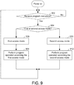
- FIG. 9 is a flowchart illustrating a program process performed by logic unit 120, according to an illustrated embodiment.
- logic unit 120 determines whether a program instruction is received (step 902). If a program instruction is not received (step 902: No), logic unit 120 repeats step 902 periodically until a program instruction is received. If a program instruction and data to be programmed are received (step 902: Yes), logic unit 120 analyzes the received program instruction to determine whether the program instruction specifies the first access mode or the second access mode (step 904). For example, logic unit 120 determines whether a program command code in the read instruction is 02(hex) or 37(hex).
- logic unit 120 determines that the program instruction specifies the first access mode (step 906). As a result, logic unit 120 performs a program operation in the first access mode (step 908). If the program command code is 37(hex), logic unit 120 determines that the received program instruction specifies the second access mode (step 910). As a result, logic unit 120 performs a program operation in the second access mode (step 912). Afterwards, logic unit 120 returns to step 902 to determine whether a program instruction is received.
- logic unit 120 can perform a program operation according to the access information stored in non-volatile memory 140 and loaded in internal register 124.
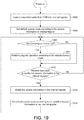
- FIG. 10 is a flowchart illustrating a program process performed by logic unit 120, according to such an embodiment.
- logic unit 120 when memory device 100 is powered on, logic unit 120 loads the access information from non-volatile memory 140 into internal register 124 of logic unit 120 (step 1002). Logic unit 120 then sets its default access mode according to the access information in internal register 124 (step 1004). Logic unit 120 determines whether a program instruction is received (step 1006). If a program instruction is not received (step 1006: No), logic unit 120 directly move to step 1010. If a program instruction is received (step 1006: Yes), logic unit 120 performs a program operation according to the default access mode (step 1008).
- Logic unit 120 determines whether an instruction to modify the access information in internal register 124 is received (step 1010). If an instruction to modify the access information in internal register 124 is not received (step 1010: No), logic unit 120 returns to step 1006 to determine whether a read instruction is received. If an instruction to modify the access information in internal register 124 is received (step 1010: Yes), logic unit 120 modifies the access information according to the received instruction (step 1012). Logic unit 120 then sets its default access mode according to the modified access information in internal register 124 (step 1014). Afterwards, logic unit 120 returns to step 1006 to determine whether a program instruction is received.
- logic unit 120 of memory device 100 can receive an erase instruction that includes information related to whether to erase a selected array block 200, or to erase a selected extra array block 210, or to erase both a selected array block 200 and a corresponding extra array block 210.
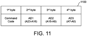
- FIG. 11 schematically illustrates an erase instruction 1100 for performing an erase operation, according to such an embodiment.
- erase instruction 1100 includes a total of four (4) bytes, i.e., a first (1st) byte, a second (2nd) byte, a third (3rd) byte, and a fourth (4th) byte.
- the first (1st) byte includes an erase command code, which can be pre-defined to instruct logic unit 120 to perform an erase operation to erase a selected array block 200, or to erase a selected extra array block 210, or to erase both a selected array block 200 and its corresponding extra array block 210.
- the second (2nd) through fourth (4th) bytes include address segments AD1, AD2, and AD3, respectively.
- the address segments AD1, AD2, and AD3 constitute a 24-bit address, which represents a location of a block to be erased.
- an erase command code of 52(hex) can be pre-defined to instruct logic unit 120 to perform an erase operation to erase a selected array block 200.
- logic unit 120 receives an instruction including 52(hex) followed by a 24-bit address, logic unit 120 performs an erase operation to erase an array block 200 having the 24-bit address.
- an erase command code of 53(hex) can be pre-defined to instruct logic unit 120 to perform an erase operation to erase a selected extra array block 210.
- logic unit 120 When logic unit 120 receives an instruction including 53(hex) followed by a 24-bit address, logic unit 120 performs an erase operation to erase an extra array block 210 having the 24-bit address.
- an erase command code of 54(hex) can be pre-defined to instruct logic unit 120 to perform an erase operation to erase both a selected array block 200 and its corresponding extra array block 210.
- logic unit 120 receives an instruction including 54(hex) followed by a 24-bit address
- logic unit 120 When logic unit 120 receives an instruction including 54(hex) followed by a 24-bit address, logic unit 120 performs an erase operation to erase an array block 200 having the 24-bit address, and an extra array block 210 corresponding to the array block 200 having the 24-bit address.
Claims (15)
- Speichervorrichtung (100), umfassend:ein Speicher-Array (130), das eine Vielzahl von Seiten (220) zum Speichern von Array-Daten und eine Vielzahl von zusätzlichen Arrays (230), die jeweils der Vielzahl von Seiten (220) zum Speichern von zusätzlichen Daten entsprechen, umfasst;eine Logikeinheit (120), die kommunikationsmäßig mit dem Speicher-Array (130) gekoppelt ist und konfiguriert ist zum:Empfangen einer Leseanweisung (400); undAusführen eines Lesevorgangs in einem ersten Zugriffsmodus (606) oder in einem zweiten Zugriffsmodus (610),dadurch gekennzeichnet, dassin dem ersten Zugriffsmodus die Logikeinheit die Array-Daten, die auf der Vielzahl von Seiten (220) gespeichert sind, sequenziell ausliest, undin dem zweiten Zugriffsmodus die Logikeinheit (120) die Array-Daten, die auf der Vielzahl von Seiten (220) gespeichert sind, und die zusätzlichen Daten, die in der Vielzahl von zusätzlichen Arrays (230) gespeichert sind, sequenziell ausliest.
- Speichervorrichtung nach Anspruch 1, wobei
die Leseanweisung vorgibt, ob der Lesevorgang in dem ersten Zugriffsmodus oder in dem zweiten Zugriffsmodus auszuführen ist;
die Leseanweisung (400) einen Lesebefehlscode und eine Startadresse für den Lesevorgang umfasst, und
der Lesebefehlscode einer von einem ersten Lesebefehlscode, der den ersten Zugriffsmodus vorgibt, und einem zweiten Lesebefehlscode, der den zweiten Zugriffsmodus und eine Größe von jedem von der Vielzahl von zusätzlichen Arrays (230) vorgibt, ist;
wobei die Logikeinheit (120) konfiguriert ist zum:Bestimmen, ob der Lesebefehlscode, der in der Leseanweisung (400) enthalten ist, der erste Lesebefehlscode oder der zweite Lesebefehlscode ist;falls bestimmt wird, dass der Lesebefehlscode der erste Lesebefehlscode ist, Ausführen des Lesevorgangs in dem ersten Zugriffsmodus; undfalls bestimmt wird, dass der Lesebefehlscode der zweite Lesebefehlscode ist, Ausführen des Lesevorgangs in dem zweiten Zugriffsmodus. - Speichervorrichtung nach Anspruch 1 oder 2, ferner umfassend einen nicht flüchtigen Speicher, der Speicherzugriffsinformationen umfasst, die vorgeben, ob ein Speicherzugriffsvorgang in dem ersten Zugriffsmodus oder dem zweiten Zugriffsmodus auszuführen ist, wobei die Logikeinheit (120) ein internes Register (124) umfasst,
wobei die Logikeinheit (120) konfiguriert ist zum:Laden der Zugriffsinformationen aus dem nicht flüchtigen Speicher in das interne Register (702); undEinstellen eines Standardzugriffsmodus gemäß den Zugriffsinformationen in dem internen Register (704). - Speichervorrichtung nach Anspruch 3, wobei die Logikeinheit (120) konfiguriert ist zum:Ausführen des Lesevorgangs in dem Standardzugriffsmodus (708).
- Speichervorrichtung nach Anspruch 3 oder 4, wobei die Logikeinheit konfiguriert ist zum:Empfangen einer Anweisung, die Zugriffsinformationen in dem internen Register (710) zu ändern;Ändern der Zugriffsinformationen in dem internen Register (712) gemäß der empfangenen Anweisung; undEinstellen des Standardzugriffsmodus gemäß der geänderten Zugriffsinformationen (714).
- Speichervorrichtung nach einem der Ansprüche 3 bis 5, wobei die Logikeinheit (120) konfiguriert ist zum:Empfangen einer Programmanweisung, die eine Adresse einer ausgewählten Seite und zu programmierende Daten umfasst; undAusführen eines Programmiervorgangs im Standardzugriffsmodus.
- Speichervorrichtung nach einem der Ansprüche 1 bis 6, wobei die Logikeinheit konfiguriert ist zum:Empfangen einer Programmanweisung (800), die eine Adresse einer ausgewählten Seite und zu programmierende Daten umfasst;Ausführen eines Programmiervorgangs in dem ersten Zugriffsmodus (906) oder dem zweiten Zugriffsmodus (910),wobeiim ersten Zugriffsmodus die Logikeinheit (120) die empfangenen Daten auf der ausgewählten Seite (220) programmiert, undim zweiten Zugriffsmodus die Logikeinheit (120) die empfangenen Daten auf der ausgewählten Seite (220) und dem zusätzlichen Array (230), das der ausgewählten Seite (220) entspricht, programmiert;wobei die Programmanweisung (800) einen Programmbefehlscode umfasst, undder Programmbefehlscode einer von einem ersten Programmbefehlscode, der den ersten Zugriffsmodus vorgibt, und einem zweiten Programmbefehlscode, der den zweiten Zugriffsmodus und die Größe von jedem von der Vielzahl von zusätzlichen Arrays vorgibt, ist.
- Speichervorrichtung nach Anspruch 7, wobei die Logikeinheit (120) konfiguriert ist zum:Bestimmen, ob der Programmbefehlscode, der in der Programmanweisung enthalten ist, der erste Programmbefehlscode oder der zweite Programmbefehlscode ist;falls bestimmt wird, dass der Programmbefehlscode der erste Programmbefehlscode ist, Ausführen des Programmiervorgangs in dem ersten Zugriffsmodus (906); undfalls bestimmt wird, dass der Programmbefehlscode der zweite Programmbefehlscode ist, Ausführen des Programmiervorgangs in dem zweiten Zugriffsmodus (910).
- Speichervorrichtung nach einem der Ansprüche 1 bis 8, wobei die Logikeinheit (120) konfiguriert ist zum:Empfangen einer Löschanweisung (1100), die eine Adresse umfasst;Bestimmen, ob die Löschanweisung (1100) das Löschen eines Array-Blocks (200), der die Adresse aufweist, oder das Löschen eines zusätzlichen Array-Blocks (210), der die Adresse aufweist, oder das Löschen eines Array-Blocks (200) und eines entsprechenden zusätzlichen Array-Blocks (210), welche die Adresse aufweisen, vorgibt; undAusführen eines Löschvorgangs basierend auf der Bestimmung.
- Speichervorrichtung (100), umfassend:ein Speicher-Array (130), das eine Vielzahl von Seiten (220) zum Speichern von Array-Daten und eine Vielzahl von zusätzlichen Arrays (230), die jeweils der Vielzahl von Seiten (220) zum Speichern zusätzlicher Daten entsprechen, umfasst;eine Logikeinheit (120), die kommunikationsmäßig mit dem Speicher-Array (130) gekoppelt ist, und konfiguriert ist zum:Empfangen einer Programmanweisung (800), die eine Adresse einer ausgewählten Seite und zu programmierende Daten umfasst;Ausführen eines Programmiervorgangs in einem ersten Zugriffsmodus (906) oder in einem zweiten Zugriffsmodus (910),wobeiin dem ersten Zugriffsmodus die Logikeinheit (120) die empfangenen Daten auf der ausgewählten Seite (220) programmiert, undin dem zweiten Zugriffsmodus die Logikeinheit (120) die empfangenen Daten auf der ausgewählten Seite (120) und in dem zusätzlichen Array (230), das der ausgewählten Seite (220) entspricht, programmiert,dadurch gekennzeichnet, dassdie Programmanweisung (800) vorgibt, ob der Programmiervorgang in dem ersten Zugriffsmodus oder dem zweiten Zugriffsmodus auszuführen ist.
- Speichervorrichtung nach Anspruch 10, wobei
die Programmanweisung einen Programmbefehlscode umfasst, und
der Programmbefehlscode einer von einem ersten Programmbefehlscode, der den ersten Zugriffsmodus vorgibt, und einem zweiten Programmbefehlscode, der den zweiten Zugriffsmodus und die Größe von jedem von der Vielzahl von zusätzlichen Arrays (230) vorgibt, ist. - Speichervorrichtung nach Anspruch 11, wobei die Logikeinheit (120) konfiguriert ist zum:Bestimmen, ob der Programmbefehlscode, der in der Programmanweisung enthalten ist, der erste Programmbefehlscode oder der zweite Programmbefehlscode ist;falls bestimmt wird, dass der Programmbefehlscode der erste Programmbefehlscode ist, Ausführen des Programmiervorgangs im ersten Zugriffsmodus; undfalls bestimmt wird, dass der Programmbefehlscode der zweite Programmbefehlscode ist, Ausführen des Programmiervorgangs im zweiten Zugriffsmodus.
- Speichervorrichtung nach einem der Ansprüche 10 bis 12, ferner umfassend einen nicht flüchtigen Speicher, der Zugriffsinformationen speichert, die vorgeben, ob ein Speicherzugriffsvorgang in dem ersten Zugriffsmodus oder dem zweiten Zugriffsmodus auszuführen ist;
wobei die Speicherlogikeinheit (120) ein internes Register (124) umfasst, und die Logikeinheit (120) konfiguriert ist zum:Laden der Zugriffsinformationen aus dem nicht flüchtigen Speicher in das interne Register (1002);Einstellen eines Standardzugriffsmodus gemäß den Zugriffsinformationen in dem internen Register (1004); undAusführen des Programmiervorgangs gemäß dem Standardzugriffsmodus (1008). - Speichervorrichtung nach Anspruch 13, wobei die Logikeinheit (120) konfiguriert ist zum:Empfangen einer Anweisung, um die Zugriffsinformationen in dem internen Register (1010) zu ändern;Ändern der Zugriffsinformationen in dem internen Register (124) gemäß der empfangenen Anweisung (1012); undEinstellen des Standardzugriffsmodus gemäß der geänderten Zugriffsinformationen (1014).
- Verfahren zum Betätigen einer Speichervorrichtung (100), wobei die Speichervorrichtung (100) eine Vielzahl von Array-Blöcken (200) zum Speichern von Array-Daten und eine Vielzahl von zusätzlichen Array-Blöcken (210), die jeweils der Vielzahl von Array-Blöcken (200) zum Speichern von zusätzlichen Daten entsprechen, umfasst, wobei das Verfahren die Schritte umfasst:Empfangen einer Leseanweisung (1100), die einen Lesebefehlscode umfasst; undBestimmen, ob der Lesebefehlscode ein erster Lesebefehlscode oder ein zweiter Lesebefehlscode ist,gekennzeichnet durchfalls bestimmt wird, dass der Lesebefehlscode der erste Lesebefehlscode ist, sequenzielles Auslesen der Array-Daten, die auf der Vielzahl von Seiten (220) gespeichert sind; undfalls bestimmt wird, dass der Lesebefehlscode der zweite Lesebefehlscode ist, sequenzielles Auslesen der Array-Daten, die auf der Vielzahl von Seiten (220) gespeichert sind, und der zusätzlichen Daten, die in der Vielzahl von zusätzlichen Arrays (230) gespeichert sind.
Applications Claiming Priority (1)
| Application Number | Priority Date | Filing Date | Title |
|---|---|---|---|
| US14/619,810 US9396769B1 (en) | 2015-02-11 | 2015-02-11 | Memory device and operating method of same |
Publications (2)
| Publication Number | Publication Date |
|---|---|
| EP3057100A1 EP3057100A1 (de) | 2016-08-17 |
| EP3057100B1 true EP3057100B1 (de) | 2017-11-22 |
Family
ID=53264518
Family Applications (1)
| Application Number | Title | Priority Date | Filing Date |
|---|---|---|---|
| EP15168965.0A Active EP3057100B1 (de) | 2015-02-11 | 2015-05-22 | Speichervorrichtung und betriebsverfahren dafür |
Country Status (3)
| Country | Link |
|---|---|
| US (1) | US9396769B1 (de) |
| EP (1) | EP3057100B1 (de) |
| CN (1) | CN106155567B (de) |
Families Citing this family (4)
| Publication number | Priority date | Publication date | Assignee | Title |
|---|---|---|---|---|
| US9886194B2 (en) * | 2015-07-13 | 2018-02-06 | Samsung Electronics Co., Ltd. | NVDIMM adaptive access mode and smart partition mechanism |
| US10658046B2 (en) * | 2017-05-26 | 2020-05-19 | Macronix International Co., Ltd. | Memory device and method for operating the same |
| CN112052189B (zh) * | 2019-06-06 | 2024-05-07 | 旺宏电子股份有限公司 | 存储器装置、电子装置以及与其相关的读取方法 |
| CN113721853B (zh) * | 2021-08-31 | 2022-08-30 | 浩鲸云计算科技股份有限公司 | 一种基于NVMe多路径负载均衡的实现方法 |
Family Cites Families (4)
| Publication number | Priority date | Publication date | Assignee | Title |
|---|---|---|---|---|
| US7259989B2 (en) * | 2004-09-03 | 2007-08-21 | Matsushita Electric Industrial Co., Ltd. | Non-volatile memory device |
| KR101666987B1 (ko) * | 2010-04-20 | 2016-10-17 | 삼성전자주식회사 | 메모리 시스템 및 그것의 동작 방법 |
| JP2013069381A (ja) * | 2011-09-22 | 2013-04-18 | Toshiba Corp | 半導体記憶装置 |
| JP2014126989A (ja) * | 2012-12-26 | 2014-07-07 | Sony Corp | 制御装置、制御方法、及び、プログラム |
-
2015
- 2015-02-11 US US14/619,810 patent/US9396769B1/en active Active
- 2015-04-02 CN CN201510154201.1A patent/CN106155567B/zh active Active
- 2015-05-22 EP EP15168965.0A patent/EP3057100B1/de active Active
Non-Patent Citations (1)
| Title |
|---|
| None * |
Also Published As
| Publication number | Publication date |
|---|---|
| CN106155567A (zh) | 2016-11-23 |
| US20160232950A1 (en) | 2016-08-11 |
| US9396769B1 (en) | 2016-07-19 |
| EP3057100A1 (de) | 2016-08-17 |
| CN106155567B (zh) | 2019-05-31 |
Similar Documents
| Publication | Publication Date | Title |
|---|---|---|
| KR100531192B1 (ko) | 비휘발성 메모리의 제어방법 | |
| EP2306321B1 (de) | Erhöhung der Speicherleistung in Flash-Speichervorrichtungen mittels gleichzeitiger Durchführung des Schreibvorgangs auf mehreren Vorrichtungen | |
| KR100897591B1 (ko) | 비-휘발성 메모리에 대해 신뢰성이 높은 데이터 복사작동을 위한 신규 방법 및 구조 | |
| EP1242868B1 (de) | Ordnung von blöcken innerhalb eines nicht-flüchtligen speichers zur erheblichen reduzierung der schreibezeit in einem sektor | |
| US6757800B1 (en) | Increasing the memory performance of flash memory devices by writing sectors simultaneously to multiple flash memory devices | |
| CN109062827B (zh) | 闪存控制装置、闪存控制系统以及闪存控制方法 | |
| KR100546348B1 (ko) | 플래시 메모리 시스템 및 그 데이터 저장 방법 | |
| US6906961B2 (en) | Erase block data splitting | |
| US6728851B1 (en) | Increasing the memory performance of flash memory devices by writing sectors simultaneously to multiple flash memory devices | |
| TWI470429B (zh) | 記憶體裝置及記憶體存取方法 | |
| KR101950758B1 (ko) | 반도체 장치 | |
| WO2002075745A1 (en) | Storage device, storage device controlling method, and program | |
| EP3057100B1 (de) | Speichervorrichtung und betriebsverfahren dafür | |
| US20090204748A1 (en) | Multi-channel flash memory system and access method | |
| CN107045423B (zh) | 存储器装置及其数据存取方法 | |
| US10176876B2 (en) | Memory control method and apparatus for programming and erasing areas | |
| US11216381B2 (en) | Data storage devices and data processing methods | |
| KR100837273B1 (ko) | 플래시 메모리 장치 | |
| US6549468B2 (en) | Non-volatile memory with address descrambling | |
| KR100737919B1 (ko) | 낸드 플래시 메모리의 프로그램 방법 및 메모리 시스템의프로그램 방법 | |
| JP4697146B2 (ja) | メモリコントローラ及びメモリコントローラを備えるフラッシュメモリシステム、並びにフラッシュメモリの制御方法 | |
| JP2004039055A (ja) | 不揮発性半導体記憶装置 | |
| KR100965079B1 (ko) | 불휘발성 메모리 장치 | |
| KR20100068469A (ko) | 반도체 기억 장치와 그 제어 방법, 전자 기기, 및 제어 장치 | |
| JP2008077468A (ja) | メモリコントローラ及びメモリコントローラを備えるフラッシュメモリシステム、並びにフラッシュメモリの制御方法 |
Legal Events
| Date | Code | Title | Description |
|---|---|---|---|
| PUAI | Public reference made under article 153(3) epc to a published international application that has entered the european phase |
Free format text: ORIGINAL CODE: 0009012 |
|
| AK | Designated contracting states |
Kind code of ref document: A1 Designated state(s): AL AT BE BG CH CY CZ DE DK EE ES FI FR GB GR HR HU IE IS IT LI LT LU LV MC MK MT NL NO PL PT RO RS SE SI SK SM TR |
|
| AX | Request for extension of the european patent |
Extension state: BA ME |
|
| 17P | Request for examination filed |
Effective date: 20160819 |
|
| RBV | Designated contracting states (corrected) |
Designated state(s): AL AT BE BG CH CY CZ DE DK EE ES FI FR GB GR HR HU IE IS IT LI LT LU LV MC MK MT NL NO PL PT RO RS SE SI SK SM TR |
|
| GRAP | Despatch of communication of intention to grant a patent |
Free format text: ORIGINAL CODE: EPIDOSNIGR1 |
|
| STAA | Information on the status of an ep patent application or granted ep patent |
Free format text: STATUS: GRANT OF PATENT IS INTENDED |
|
| RIC1 | Information provided on ipc code assigned before grant |
Ipc: G06F 12/02 20060101ALI20170609BHEP Ipc: G11C 16/06 20060101ALI20170609BHEP Ipc: G11C 7/10 20060101AFI20170609BHEP Ipc: G11C 7/00 20060101ALI20170609BHEP |
|
| INTG | Intention to grant announced |
Effective date: 20170626 |
|
| GRAS | Grant fee paid |
Free format text: ORIGINAL CODE: EPIDOSNIGR3 |
|
| GRAA | (expected) grant |
Free format text: ORIGINAL CODE: 0009210 |
|
| STAA | Information on the status of an ep patent application or granted ep patent |
Free format text: STATUS: THE PATENT HAS BEEN GRANTED |
|
| AK | Designated contracting states |
Kind code of ref document: B1 Designated state(s): AL AT BE BG CH CY CZ DE DK EE ES FI FR GB GR HR HU IE IS IT LI LT LU LV MC MK MT NL NO PL PT RO RS SE SI SK SM TR |
|
| REG | Reference to a national code |
Ref country code: GB Ref legal event code: FG4D |
|
| REG | Reference to a national code |
Ref country code: CH Ref legal event code: EP |
|
| REG | Reference to a national code |
Ref country code: IE Ref legal event code: FG4D |
|
| REG | Reference to a national code |
Ref country code: AT Ref legal event code: REF Ref document number: 949096 Country of ref document: AT Kind code of ref document: T Effective date: 20171215 |
|
| REG | Reference to a national code |
Ref country code: DE Ref legal event code: R096 Ref document number: 602015006113 Country of ref document: DE |
|
| REG | Reference to a national code |
Ref country code: NL Ref legal event code: FP |
|
| REG | Reference to a national code |
Ref country code: FR Ref legal event code: PLFP Year of fee payment: 4 |
|
| REG | Reference to a national code |
Ref country code: LT Ref legal event code: MG4D |
|
| REG | Reference to a national code |
Ref country code: AT Ref legal event code: MK05 Ref document number: 949096 Country of ref document: AT Kind code of ref document: T Effective date: 20171122 |
|
| PG25 | Lapsed in a contracting state [announced via postgrant information from national office to epo] |
Ref country code: ES Free format text: LAPSE BECAUSE OF FAILURE TO SUBMIT A TRANSLATION OF THE DESCRIPTION OR TO PAY THE FEE WITHIN THE PRESCRIBED TIME-LIMIT Effective date: 20171122 Ref country code: LT Free format text: LAPSE BECAUSE OF FAILURE TO SUBMIT A TRANSLATION OF THE DESCRIPTION OR TO PAY THE FEE WITHIN THE PRESCRIBED TIME-LIMIT Effective date: 20171122 Ref country code: SE Free format text: LAPSE BECAUSE OF FAILURE TO SUBMIT A TRANSLATION OF THE DESCRIPTION OR TO PAY THE FEE WITHIN THE PRESCRIBED TIME-LIMIT Effective date: 20171122 Ref country code: FI Free format text: LAPSE BECAUSE OF FAILURE TO SUBMIT A TRANSLATION OF THE DESCRIPTION OR TO PAY THE FEE WITHIN THE PRESCRIBED TIME-LIMIT Effective date: 20171122 Ref country code: NO Free format text: LAPSE BECAUSE OF FAILURE TO SUBMIT A TRANSLATION OF THE DESCRIPTION OR TO PAY THE FEE WITHIN THE PRESCRIBED TIME-LIMIT Effective date: 20180222 |
|
| PG25 | Lapsed in a contracting state [announced via postgrant information from national office to epo] |
Ref country code: HR Free format text: LAPSE BECAUSE OF FAILURE TO SUBMIT A TRANSLATION OF THE DESCRIPTION OR TO PAY THE FEE WITHIN THE PRESCRIBED TIME-LIMIT Effective date: 20171122 Ref country code: LV Free format text: LAPSE BECAUSE OF FAILURE TO SUBMIT A TRANSLATION OF THE DESCRIPTION OR TO PAY THE FEE WITHIN THE PRESCRIBED TIME-LIMIT Effective date: 20171122 Ref country code: RS Free format text: LAPSE BECAUSE OF FAILURE TO SUBMIT A TRANSLATION OF THE DESCRIPTION OR TO PAY THE FEE WITHIN THE PRESCRIBED TIME-LIMIT Effective date: 20171122 Ref country code: AT Free format text: LAPSE BECAUSE OF FAILURE TO SUBMIT A TRANSLATION OF THE DESCRIPTION OR TO PAY THE FEE WITHIN THE PRESCRIBED TIME-LIMIT Effective date: 20171122 Ref country code: BG Free format text: LAPSE BECAUSE OF FAILURE TO SUBMIT A TRANSLATION OF THE DESCRIPTION OR TO PAY THE FEE WITHIN THE PRESCRIBED TIME-LIMIT Effective date: 20180222 Ref country code: GR Free format text: LAPSE BECAUSE OF FAILURE TO SUBMIT A TRANSLATION OF THE DESCRIPTION OR TO PAY THE FEE WITHIN THE PRESCRIBED TIME-LIMIT Effective date: 20180223 |
|
| PG25 | Lapsed in a contracting state [announced via postgrant information from national office to epo] |
Ref country code: DK Free format text: LAPSE BECAUSE OF FAILURE TO SUBMIT A TRANSLATION OF THE DESCRIPTION OR TO PAY THE FEE WITHIN THE PRESCRIBED TIME-LIMIT Effective date: 20171122 Ref country code: EE Free format text: LAPSE BECAUSE OF FAILURE TO SUBMIT A TRANSLATION OF THE DESCRIPTION OR TO PAY THE FEE WITHIN THE PRESCRIBED TIME-LIMIT Effective date: 20171122 Ref country code: CY Free format text: LAPSE BECAUSE OF FAILURE TO SUBMIT A TRANSLATION OF THE DESCRIPTION OR TO PAY THE FEE WITHIN THE PRESCRIBED TIME-LIMIT Effective date: 20171122 Ref country code: SK Free format text: LAPSE BECAUSE OF FAILURE TO SUBMIT A TRANSLATION OF THE DESCRIPTION OR TO PAY THE FEE WITHIN THE PRESCRIBED TIME-LIMIT Effective date: 20171122 Ref country code: CZ Free format text: LAPSE BECAUSE OF FAILURE TO SUBMIT A TRANSLATION OF THE DESCRIPTION OR TO PAY THE FEE WITHIN THE PRESCRIBED TIME-LIMIT Effective date: 20171122 |
|
| REG | Reference to a national code |
Ref country code: DE Ref legal event code: R097 Ref document number: 602015006113 Country of ref document: DE |
|
| PG25 | Lapsed in a contracting state [announced via postgrant information from national office to epo] |
Ref country code: SM Free format text: LAPSE BECAUSE OF FAILURE TO SUBMIT A TRANSLATION OF THE DESCRIPTION OR TO PAY THE FEE WITHIN THE PRESCRIBED TIME-LIMIT Effective date: 20171122 Ref country code: RO Free format text: LAPSE BECAUSE OF FAILURE TO SUBMIT A TRANSLATION OF THE DESCRIPTION OR TO PAY THE FEE WITHIN THE PRESCRIBED TIME-LIMIT Effective date: 20171122 Ref country code: IT Free format text: LAPSE BECAUSE OF FAILURE TO SUBMIT A TRANSLATION OF THE DESCRIPTION OR TO PAY THE FEE WITHIN THE PRESCRIBED TIME-LIMIT Effective date: 20171122 Ref country code: PL Free format text: LAPSE BECAUSE OF FAILURE TO SUBMIT A TRANSLATION OF THE DESCRIPTION OR TO PAY THE FEE WITHIN THE PRESCRIBED TIME-LIMIT Effective date: 20171122 |
|
| PLBE | No opposition filed within time limit |
Free format text: ORIGINAL CODE: 0009261 |
|
| STAA | Information on the status of an ep patent application or granted ep patent |
Free format text: STATUS: NO OPPOSITION FILED WITHIN TIME LIMIT |
|
| 26N | No opposition filed |
Effective date: 20180823 |
|
| PG25 | Lapsed in a contracting state [announced via postgrant information from national office to epo] |
Ref country code: SI Free format text: LAPSE BECAUSE OF FAILURE TO SUBMIT A TRANSLATION OF THE DESCRIPTION OR TO PAY THE FEE WITHIN THE PRESCRIBED TIME-LIMIT Effective date: 20171122 |
|
| REG | Reference to a national code |
Ref country code: CH Ref legal event code: PL |
|
| REG | Reference to a national code |
Ref country code: BE Ref legal event code: MM Effective date: 20180531 |
|
| PG25 | Lapsed in a contracting state [announced via postgrant information from national office to epo] |
Ref country code: MC Free format text: LAPSE BECAUSE OF FAILURE TO SUBMIT A TRANSLATION OF THE DESCRIPTION OR TO PAY THE FEE WITHIN THE PRESCRIBED TIME-LIMIT Effective date: 20171122 |
|
| REG | Reference to a national code |
Ref country code: IE Ref legal event code: MM4A |
|
| PG25 | Lapsed in a contracting state [announced via postgrant information from national office to epo] |
Ref country code: LI Free format text: LAPSE BECAUSE OF NON-PAYMENT OF DUE FEES Effective date: 20180531 Ref country code: CH Free format text: LAPSE BECAUSE OF NON-PAYMENT OF DUE FEES Effective date: 20180531 |
|
| PG25 | Lapsed in a contracting state [announced via postgrant information from national office to epo] |
Ref country code: LU Free format text: LAPSE BECAUSE OF NON-PAYMENT OF DUE FEES Effective date: 20180522 |
|
| PG25 | Lapsed in a contracting state [announced via postgrant information from national office to epo] |
Ref country code: IE Free format text: LAPSE BECAUSE OF NON-PAYMENT OF DUE FEES Effective date: 20180522 |
|
| PG25 | Lapsed in a contracting state [announced via postgrant information from national office to epo] |
Ref country code: BE Free format text: LAPSE BECAUSE OF NON-PAYMENT OF DUE FEES Effective date: 20180531 |
|
| PG25 | Lapsed in a contracting state [announced via postgrant information from national office to epo] |
Ref country code: MT Free format text: LAPSE BECAUSE OF NON-PAYMENT OF DUE FEES Effective date: 20180522 |
|
| PG25 | Lapsed in a contracting state [announced via postgrant information from national office to epo] |
Ref country code: TR Free format text: LAPSE BECAUSE OF FAILURE TO SUBMIT A TRANSLATION OF THE DESCRIPTION OR TO PAY THE FEE WITHIN THE PRESCRIBED TIME-LIMIT Effective date: 20171122 |
|
| PG25 | Lapsed in a contracting state [announced via postgrant information from national office to epo] |
Ref country code: PT Free format text: LAPSE BECAUSE OF FAILURE TO SUBMIT A TRANSLATION OF THE DESCRIPTION OR TO PAY THE FEE WITHIN THE PRESCRIBED TIME-LIMIT Effective date: 20171122 |
|
| PG25 | Lapsed in a contracting state [announced via postgrant information from national office to epo] |
Ref country code: MK Free format text: LAPSE BECAUSE OF NON-PAYMENT OF DUE FEES Effective date: 20171122 Ref country code: HU Free format text: LAPSE BECAUSE OF FAILURE TO SUBMIT A TRANSLATION OF THE DESCRIPTION OR TO PAY THE FEE WITHIN THE PRESCRIBED TIME-LIMIT; INVALID AB INITIO Effective date: 20150522 |
|
| PG25 | Lapsed in a contracting state [announced via postgrant information from national office to epo] |
Ref country code: AL Free format text: LAPSE BECAUSE OF FAILURE TO SUBMIT A TRANSLATION OF THE DESCRIPTION OR TO PAY THE FEE WITHIN THE PRESCRIBED TIME-LIMIT Effective date: 20171122 Ref country code: IS Free format text: LAPSE BECAUSE OF FAILURE TO SUBMIT A TRANSLATION OF THE DESCRIPTION OR TO PAY THE FEE WITHIN THE PRESCRIBED TIME-LIMIT Effective date: 20180322 |
|
| PGFP | Annual fee paid to national office [announced via postgrant information from national office to epo] |
Ref country code: FR Payment date: 20230330 Year of fee payment: 9 |
|
| P01 | Opt-out of the competence of the unified patent court (upc) registered |
Effective date: 20230526 |
|
| PGFP | Annual fee paid to national office [announced via postgrant information from national office to epo] |
Ref country code: DE Payment date: 20230316 Year of fee payment: 9 |
|
| PGFP | Annual fee paid to national office [announced via postgrant information from national office to epo] |
Ref country code: NL Payment date: 20240308 Year of fee payment: 10 |
|
| PGFP | Annual fee paid to national office [announced via postgrant information from national office to epo] |
Ref country code: GB Payment date: 20240307 Year of fee payment: 10 |