EP3055892B1 - Laminat für eine lichtemittierende vorrichtung und verfahren zur herstellung davon - Google Patents
Laminat für eine lichtemittierende vorrichtung und verfahren zur herstellung davon Download PDFInfo
- Publication number
- EP3055892B1 EP3055892B1 EP14851475.5A EP14851475A EP3055892B1 EP 3055892 B1 EP3055892 B1 EP 3055892B1 EP 14851475 A EP14851475 A EP 14851475A EP 3055892 B1 EP3055892 B1 EP 3055892B1
- Authority
- EP
- European Patent Office
- Prior art keywords
- weight
- glass frit
- layer
- laminate
- reliefs
- Prior art date
- Legal status (The legal status is an assumption and is not a legal conclusion. Google has not performed a legal analysis and makes no representation as to the accuracy of the status listed.)
- Not-in-force
Links
- 238000000034 method Methods 0.000 title claims description 58
- 230000008569 process Effects 0.000 title claims description 45
- 239000011521 glass Substances 0.000 claims description 273
- 239000000758 substrate Substances 0.000 claims description 91
- 238000005245 sintering Methods 0.000 claims description 65
- XLOMVQKBTHCTTD-UHFFFAOYSA-N Zinc monoxide Chemical compound [Zn]=O XLOMVQKBTHCTTD-UHFFFAOYSA-N 0.000 claims description 36
- VYPSYNLAJGMNEJ-UHFFFAOYSA-N Silicium dioxide Chemical compound O=[Si]=O VYPSYNLAJGMNEJ-UHFFFAOYSA-N 0.000 claims description 26
- 239000011295 pitch Substances 0.000 claims description 25
- GWEVSGVZZGPLCZ-UHFFFAOYSA-N Titan oxide Chemical compound O=[Ti]=O GWEVSGVZZGPLCZ-UHFFFAOYSA-N 0.000 claims description 21
- WMWLMWRWZQELOS-UHFFFAOYSA-N bismuth(iii) oxide Chemical compound O=[Bi]O[Bi]=O WMWLMWRWZQELOS-UHFFFAOYSA-N 0.000 claims description 18
- JKWMSGQKBLHBQQ-UHFFFAOYSA-N diboron trioxide Chemical compound O=BOB=O JKWMSGQKBLHBQQ-UHFFFAOYSA-N 0.000 claims description 18
- 239000000843 powder Substances 0.000 claims description 18
- KKCBUQHMOMHUOY-UHFFFAOYSA-N Na2O Inorganic materials [O-2].[Na+].[Na+] KKCBUQHMOMHUOY-UHFFFAOYSA-N 0.000 claims description 17
- 238000004519 manufacturing process Methods 0.000 claims description 17
- 229910052814 silicon oxide Inorganic materials 0.000 claims description 17
- 238000002834 transmittance Methods 0.000 claims description 16
- 239000011787 zinc oxide Substances 0.000 claims description 16
- 230000015572 biosynthetic process Effects 0.000 claims description 15
- CPLXHLVBOLITMK-UHFFFAOYSA-N Magnesium oxide Chemical compound [Mg]=O CPLXHLVBOLITMK-UHFFFAOYSA-N 0.000 claims description 12
- MCMNRKCIXSYSNV-UHFFFAOYSA-N Zirconium dioxide Chemical compound O=[Zr]=O MCMNRKCIXSYSNV-UHFFFAOYSA-N 0.000 claims description 12
- 238000000059 patterning Methods 0.000 claims description 12
- 210000003298 dental enamel Anatomy 0.000 claims description 11
- CETPSERCERDGAM-UHFFFAOYSA-N ceric oxide Chemical compound O=[Ce]=O CETPSERCERDGAM-UHFFFAOYSA-N 0.000 claims description 10
- 229910000422 cerium(IV) oxide Inorganic materials 0.000 claims description 10
- 239000003960 organic solvent Substances 0.000 claims description 10
- 238000001035 drying Methods 0.000 claims description 9
- 229910052751 metal Inorganic materials 0.000 claims description 8
- 239000002184 metal Substances 0.000 claims description 8
- 230000009477 glass transition Effects 0.000 claims description 7
- FUJCRWPEOMXPAD-UHFFFAOYSA-N Li2O Inorganic materials [Li+].[Li+].[O-2] FUJCRWPEOMXPAD-UHFFFAOYSA-N 0.000 claims description 6
- 229910019714 Nb2O3 Inorganic materials 0.000 claims description 6
- 230000004888 barrier function Effects 0.000 claims description 6
- XUCJHNOBJLKZNU-UHFFFAOYSA-M dilithium;hydroxide Chemical compound [Li+].[Li+].[OH-] XUCJHNOBJLKZNU-UHFFFAOYSA-M 0.000 claims description 6
- MRELNEQAGSRDBK-UHFFFAOYSA-N lanthanum oxide Inorganic materials [O-2].[O-2].[O-2].[La+3].[La+3] MRELNEQAGSRDBK-UHFFFAOYSA-N 0.000 claims description 6
- KTUFCUMIWABKDW-UHFFFAOYSA-N oxo(oxolanthaniooxy)lanthanum Chemical compound O=[La]O[La]=O KTUFCUMIWABKDW-UHFFFAOYSA-N 0.000 claims description 6
- NOTVAPJNGZMVSD-UHFFFAOYSA-N potassium monoxide Inorganic materials [K]O[K] NOTVAPJNGZMVSD-UHFFFAOYSA-N 0.000 claims description 6
- 239000000377 silicon dioxide Substances 0.000 claims description 6
- 229910052581 Si3N4 Inorganic materials 0.000 claims description 5
- 238000005054 agglomeration Methods 0.000 claims description 5
- 230000002776 aggregation Effects 0.000 claims description 5
- 150000001875 compounds Chemical class 0.000 claims description 5
- 229910044991 metal oxide Inorganic materials 0.000 claims description 5
- 150000004706 metal oxides Chemical class 0.000 claims description 5
- 229910052709 silver Inorganic materials 0.000 claims description 5
- 239000005361 soda-lime glass Substances 0.000 claims description 5
- DLYUQMMRRRQYAE-UHFFFAOYSA-N tetraphosphorus decaoxide Chemical compound O1P(O2)(=O)OP3(=O)OP1(=O)OP2(=O)O3 DLYUQMMRRRQYAE-UHFFFAOYSA-N 0.000 claims description 5
- BQCADISMDOOEFD-UHFFFAOYSA-N Silver Chemical compound [Ag] BQCADISMDOOEFD-UHFFFAOYSA-N 0.000 claims description 4
- 239000004020 conductor Substances 0.000 claims description 4
- 229920000172 poly(styrenesulfonic acid) Polymers 0.000 claims description 4
- 229940005642 polystyrene sulfonic acid Drugs 0.000 claims description 4
- 239000004332 silver Substances 0.000 claims description 4
- XOLBLPGZBRYERU-UHFFFAOYSA-N tin dioxide Chemical compound O=[Sn]=O XOLBLPGZBRYERU-UHFFFAOYSA-N 0.000 claims description 4
- 229910003076 TiO2-Al2O3 Inorganic materials 0.000 claims description 3
- 239000000956 alloy Substances 0.000 claims description 3
- 229910045601 alloy Inorganic materials 0.000 claims description 3
- 229910052782 aluminium Inorganic materials 0.000 claims description 3
- XAGFODPZIPBFFR-UHFFFAOYSA-N aluminium Chemical compound [Al] XAGFODPZIPBFFR-UHFFFAOYSA-N 0.000 claims description 3
- 238000000280 densification Methods 0.000 claims description 3
- AMGQUBHHOARCQH-UHFFFAOYSA-N indium;oxotin Chemical compound [In].[Sn]=O AMGQUBHHOARCQH-UHFFFAOYSA-N 0.000 claims description 3
- GYHNNYVSQQEPJS-UHFFFAOYSA-N Gallium Chemical compound [Ga] GYHNNYVSQQEPJS-UHFFFAOYSA-N 0.000 claims description 2
- 229920000144 PEDOT:PSS Polymers 0.000 claims description 2
- 229920001609 Poly(3,4-ethylenedioxythiophene) Polymers 0.000 claims description 2
- 239000004411 aluminium Substances 0.000 claims description 2
- XCJYREBRNVKWGJ-UHFFFAOYSA-N copper(II) phthalocyanine Chemical compound [Cu+2].C12=CC=CC=C2C(N=C2[N-]C(C3=CC=CC=C32)=N2)=NC1=NC([C]1C=CC=CC1=1)=NC=1N=C1[C]3C=CC=CC3=C2[N-]1 XCJYREBRNVKWGJ-UHFFFAOYSA-N 0.000 claims description 2
- 229910052733 gallium Inorganic materials 0.000 claims description 2
- RBTKNAXYKSUFRK-UHFFFAOYSA-N heliogen blue Chemical compound [Cu].[N-]1C2=C(C=CC=C3)C3=C1N=C([N-]1)C3=CC=CC=C3C1=NC([N-]1)=C(C=CC=C3)C3=C1N=C([N-]1)C3=CC=CC=C3C1=N2 RBTKNAXYKSUFRK-UHFFFAOYSA-N 0.000 claims description 2
- 238000001459 lithography Methods 0.000 claims description 2
- YVTHLONGBIQYBO-UHFFFAOYSA-N zinc indium(3+) oxygen(2-) Chemical compound [O--].[Zn++].[In+3] YVTHLONGBIQYBO-UHFFFAOYSA-N 0.000 claims description 2
- PNEYBMLMFCGWSK-UHFFFAOYSA-N aluminium oxide Inorganic materials [O-2].[O-2].[O-2].[Al+3].[Al+3] PNEYBMLMFCGWSK-UHFFFAOYSA-N 0.000 claims 5
- 229910052681 coesite Inorganic materials 0.000 claims 5
- 229910052593 corundum Inorganic materials 0.000 claims 5
- 229910052906 cristobalite Inorganic materials 0.000 claims 5
- 229910052682 stishovite Inorganic materials 0.000 claims 5
- 229910052905 tridymite Inorganic materials 0.000 claims 5
- 229910001845 yogo sapphire Inorganic materials 0.000 claims 5
- 239000010410 layer Substances 0.000 description 200
- 238000000605 extraction Methods 0.000 description 64
- 230000003287 optical effect Effects 0.000 description 27
- 230000000052 comparative effect Effects 0.000 description 16
- TWNQGVIAIRXVLR-UHFFFAOYSA-N oxo(oxoalumanyloxy)alumane Chemical compound O=[Al]O[Al]=O TWNQGVIAIRXVLR-UHFFFAOYSA-N 0.000 description 16
- 239000012071 phase Substances 0.000 description 12
- 230000001965 increasing effect Effects 0.000 description 10
- 239000000203 mixture Substances 0.000 description 10
- 238000000576 coating method Methods 0.000 description 9
- 239000011230 binding agent Substances 0.000 description 8
- 239000011248 coating agent Substances 0.000 description 8
- 230000000694 effects Effects 0.000 description 8
- 239000002245 particle Substances 0.000 description 8
- 239000002904 solvent Substances 0.000 description 8
- 239000000126 substance Substances 0.000 description 8
- 239000001856 Ethyl cellulose Substances 0.000 description 6
- ZZSNKZQZMQGXPY-UHFFFAOYSA-N Ethyl cellulose Chemical compound CCOCC1OC(OC)C(OCC)C(OCC)C1OC1C(O)C(O)C(OC)C(CO)O1 ZZSNKZQZMQGXPY-UHFFFAOYSA-N 0.000 description 6
- 229920001249 ethyl cellulose Polymers 0.000 description 6
- 235000019325 ethyl cellulose Nutrition 0.000 description 6
- 238000002360 preparation method Methods 0.000 description 6
- 239000010408 film Substances 0.000 description 5
- 239000000463 material Substances 0.000 description 5
- 239000012044 organic layer Substances 0.000 description 5
- 239000005373 porous glass Substances 0.000 description 5
- 238000000149 argon plasma sintering Methods 0.000 description 4
- 230000008859 change Effects 0.000 description 4
- 230000006866 deterioration Effects 0.000 description 4
- 238000009826 distribution Methods 0.000 description 4
- 239000002086 nanomaterial Substances 0.000 description 4
- 239000002994 raw material Substances 0.000 description 4
- 238000001878 scanning electron micrograph Methods 0.000 description 4
- 238000000151 deposition Methods 0.000 description 3
- 238000010438 heat treatment Methods 0.000 description 3
- 238000005259 measurement Methods 0.000 description 3
- 239000011368 organic material Substances 0.000 description 3
- 229920000642 polymer Polymers 0.000 description 3
- 238000007650 screen-printing Methods 0.000 description 3
- 230000000087 stabilizing effect Effects 0.000 description 3
- 230000003746 surface roughness Effects 0.000 description 3
- 239000010409 thin film Substances 0.000 description 3
- 230000007704 transition Effects 0.000 description 3
- 229910052723 transition metal Inorganic materials 0.000 description 3
- 150000003624 transition metals Chemical class 0.000 description 3
- VXQBJTKSVGFQOL-UHFFFAOYSA-N 2-(2-butoxyethoxy)ethyl acetate Chemical compound CCCCOCCOCCOC(C)=O VXQBJTKSVGFQOL-UHFFFAOYSA-N 0.000 description 2
- NCGICGYLBXGBGN-UHFFFAOYSA-N 3-morpholin-4-yl-1-oxa-3-azonia-2-azanidacyclopent-3-en-5-imine;hydrochloride Chemical group Cl.[N-]1OC(=N)C=[N+]1N1CCOCC1 NCGICGYLBXGBGN-UHFFFAOYSA-N 0.000 description 2
- 238000002835 absorbance Methods 0.000 description 2
- 230000007423 decrease Effects 0.000 description 2
- 238000005516 engineering process Methods 0.000 description 2
- 238000005530 etching Methods 0.000 description 2
- 239000000284 extract Substances 0.000 description 2
- 239000007791 liquid phase Substances 0.000 description 2
- 238000001000 micrograph Methods 0.000 description 2
- 238000007639 printing Methods 0.000 description 2
- 238000012545 processing Methods 0.000 description 2
- 230000009467 reduction Effects 0.000 description 2
- 238000011160 research Methods 0.000 description 2
- 239000002356 single layer Substances 0.000 description 2
- HUAUNKAZQWMVFY-UHFFFAOYSA-M sodium;oxocalcium;hydroxide Chemical compound [OH-].[Na+].[Ca]=O HUAUNKAZQWMVFY-UHFFFAOYSA-M 0.000 description 2
- 229910052720 vanadium Inorganic materials 0.000 description 2
- 229920002799 BoPET Polymers 0.000 description 1
- OKTJSMMVPCPJKN-UHFFFAOYSA-N Carbon Chemical compound [C] OKTJSMMVPCPJKN-UHFFFAOYSA-N 0.000 description 1
- 229910052688 Gadolinium Inorganic materials 0.000 description 1
- OAICVXFJPJFONN-UHFFFAOYSA-N Phosphorus Chemical compound [P] OAICVXFJPJFONN-UHFFFAOYSA-N 0.000 description 1
- 239000002253 acid Substances 0.000 description 1
- 229910052783 alkali metal Inorganic materials 0.000 description 1
- 150000001340 alkali metals Chemical class 0.000 description 1
- 239000005388 borosilicate glass Substances 0.000 description 1
- 230000005587 bubbling Effects 0.000 description 1
- 229910052793 cadmium Inorganic materials 0.000 description 1
- 238000004364 calculation method Methods 0.000 description 1
- 238000005266 casting Methods 0.000 description 1
- 238000003486 chemical etching Methods 0.000 description 1
- 229910052804 chromium Inorganic materials 0.000 description 1
- 229910052802 copper Inorganic materials 0.000 description 1
- 239000010949 copper Substances 0.000 description 1
- 230000007812 deficiency Effects 0.000 description 1
- 238000007872 degassing Methods 0.000 description 1
- 230000008021 deposition Effects 0.000 description 1
- 238000007607 die coating method Methods 0.000 description 1
- YWEUIGNSBFLMFL-UHFFFAOYSA-N diphosphonate Chemical compound O=P(=O)OP(=O)=O YWEUIGNSBFLMFL-UHFFFAOYSA-N 0.000 description 1
- 230000002708 enhancing effect Effects 0.000 description 1
- 238000011156 evaluation Methods 0.000 description 1
- 239000002241 glass-ceramic Substances 0.000 description 1
- 229910052737 gold Inorganic materials 0.000 description 1
- 229910021389 graphene Inorganic materials 0.000 description 1
- 238000000227 grinding Methods 0.000 description 1
- 238000010191 image analysis Methods 0.000 description 1
- 229910010272 inorganic material Inorganic materials 0.000 description 1
- 239000011147 inorganic material Substances 0.000 description 1
- 229910052742 iron Inorganic materials 0.000 description 1
- 239000012939 laminating adhesive Substances 0.000 description 1
- 229910052747 lanthanoid Inorganic materials 0.000 description 1
- 150000002602 lanthanoids Chemical class 0.000 description 1
- 229910052745 lead Inorganic materials 0.000 description 1
- 230000031700 light absorption Effects 0.000 description 1
- 238000012538 light obscuration Methods 0.000 description 1
- 239000006193 liquid solution Substances 0.000 description 1
- 229910052748 manganese Inorganic materials 0.000 description 1
- 229910052750 molybdenum Inorganic materials 0.000 description 1
- 239000002105 nanoparticle Substances 0.000 description 1
- 229910052759 nickel Inorganic materials 0.000 description 1
- 238000010943 off-gassing Methods 0.000 description 1
- 229910052763 palladium Inorganic materials 0.000 description 1
- 229910052698 phosphorus Inorganic materials 0.000 description 1
- 238000000206 photolithography Methods 0.000 description 1
- 239000004038 photonic crystal Substances 0.000 description 1
- 239000010665 pine oil Substances 0.000 description 1
- 229910052697 platinum Inorganic materials 0.000 description 1
- 230000000717 retained effect Effects 0.000 description 1
- 238000005488 sandblasting Methods 0.000 description 1
- 235000012239 silicon dioxide Nutrition 0.000 description 1
- HQVNEWCFYHHQES-UHFFFAOYSA-N silicon nitride Chemical compound N12[Si]34N5[Si]62N3[Si]51N64 HQVNEWCFYHHQES-UHFFFAOYSA-N 0.000 description 1
- 238000004544 sputter deposition Methods 0.000 description 1
- 229910052718 tin Inorganic materials 0.000 description 1
- OGIDPMRJRNCKJF-UHFFFAOYSA-N titanium oxide Inorganic materials [Ti]=O OGIDPMRJRNCKJF-UHFFFAOYSA-N 0.000 description 1
- XLYOFNOQVPJJNP-UHFFFAOYSA-N water Substances O XLYOFNOQVPJJNP-UHFFFAOYSA-N 0.000 description 1
- 238000004383 yellowing Methods 0.000 description 1
Images


Classifications
-
- F—MECHANICAL ENGINEERING; LIGHTING; HEATING; WEAPONS; BLASTING
- F21—LIGHTING
- F21V—FUNCTIONAL FEATURES OR DETAILS OF LIGHTING DEVICES OR SYSTEMS THEREOF; STRUCTURAL COMBINATIONS OF LIGHTING DEVICES WITH OTHER ARTICLES, NOT OTHERWISE PROVIDED FOR
- F21V5/00—Refractors for light sources
- F21V5/002—Refractors for light sources using microoptical elements for redirecting or diffusing light
-
- C—CHEMISTRY; METALLURGY
- C03—GLASS; MINERAL OR SLAG WOOL
- C03B—MANUFACTURE, SHAPING, OR SUPPLEMENTARY PROCESSES
- C03B23/00—Re-forming shaped glass
- C03B23/20—Uniting glass pieces by fusing without substantial reshaping
-
- F—MECHANICAL ENGINEERING; LIGHTING; HEATING; WEAPONS; BLASTING
- F21—LIGHTING
- F21K—NON-ELECTRIC LIGHT SOURCES USING LUMINESCENCE; LIGHT SOURCES USING ELECTROCHEMILUMINESCENCE; LIGHT SOURCES USING CHARGES OF COMBUSTIBLE MATERIAL; LIGHT SOURCES USING SEMICONDUCTOR DEVICES AS LIGHT-GENERATING ELEMENTS; LIGHT SOURCES NOT OTHERWISE PROVIDED FOR
- F21K9/00—Light sources using semiconductor devices as light-generating elements, e.g. using light-emitting diodes [LED] or lasers
- F21K9/60—Optical arrangements integrated in the light source, e.g. for improving the colour rendering index or the light extraction
-
- F—MECHANICAL ENGINEERING; LIGHTING; HEATING; WEAPONS; BLASTING
- F21—LIGHTING
- F21K—NON-ELECTRIC LIGHT SOURCES USING LUMINESCENCE; LIGHT SOURCES USING ELECTROCHEMILUMINESCENCE; LIGHT SOURCES USING CHARGES OF COMBUSTIBLE MATERIAL; LIGHT SOURCES USING SEMICONDUCTOR DEVICES AS LIGHT-GENERATING ELEMENTS; LIGHT SOURCES NOT OTHERWISE PROVIDED FOR
- F21K9/00—Light sources using semiconductor devices as light-generating elements, e.g. using light-emitting diodes [LED] or lasers
- F21K9/90—Methods of manufacture
-
- H—ELECTRICITY
- H10—SEMICONDUCTOR DEVICES; ELECTRIC SOLID-STATE DEVICES NOT OTHERWISE PROVIDED FOR
- H10K—ORGANIC ELECTRIC SOLID-STATE DEVICES
- H10K50/00—Organic light-emitting devices
- H10K50/80—Constructional details
- H10K50/805—Electrodes
- H10K50/81—Anodes
-
- H—ELECTRICITY
- H10—SEMICONDUCTOR DEVICES; ELECTRIC SOLID-STATE DEVICES NOT OTHERWISE PROVIDED FOR
- H10K—ORGANIC ELECTRIC SOLID-STATE DEVICES
- H10K50/00—Organic light-emitting devices
- H10K50/80—Constructional details
- H10K50/805—Electrodes
- H10K50/82—Cathodes
- H10K50/828—Transparent cathodes, e.g. comprising thin metal layers
-
- H—ELECTRICITY
- H10—SEMICONDUCTOR DEVICES; ELECTRIC SOLID-STATE DEVICES NOT OTHERWISE PROVIDED FOR
- H10K—ORGANIC ELECTRIC SOLID-STATE DEVICES
- H10K50/00—Organic light-emitting devices
- H10K50/80—Constructional details
- H10K50/84—Passivation; Containers; Encapsulations
- H10K50/844—Encapsulations
-
- H—ELECTRICITY
- H10—SEMICONDUCTOR DEVICES; ELECTRIC SOLID-STATE DEVICES NOT OTHERWISE PROVIDED FOR
- H10K—ORGANIC ELECTRIC SOLID-STATE DEVICES
- H10K50/00—Organic light-emitting devices
- H10K50/80—Constructional details
- H10K50/85—Arrangements for extracting light from the devices
- H10K50/854—Arrangements for extracting light from the devices comprising scattering means
-
- H—ELECTRICITY
- H10—SEMICONDUCTOR DEVICES; ELECTRIC SOLID-STATE DEVICES NOT OTHERWISE PROVIDED FOR
- H10K—ORGANIC ELECTRIC SOLID-STATE DEVICES
- H10K50/00—Organic light-emitting devices
- H10K50/80—Constructional details
- H10K50/85—Arrangements for extracting light from the devices
- H10K50/856—Arrangements for extracting light from the devices comprising reflective means
-
- H—ELECTRICITY
- H10—SEMICONDUCTOR DEVICES; ELECTRIC SOLID-STATE DEVICES NOT OTHERWISE PROVIDED FOR
- H10K—ORGANIC ELECTRIC SOLID-STATE DEVICES
- H10K50/00—Organic light-emitting devices
- H10K50/80—Constructional details
- H10K50/85—Arrangements for extracting light from the devices
- H10K50/858—Arrangements for extracting light from the devices comprising refractive means, e.g. lenses
-
- H—ELECTRICITY
- H10—SEMICONDUCTOR DEVICES; ELECTRIC SOLID-STATE DEVICES NOT OTHERWISE PROVIDED FOR
- H10K—ORGANIC ELECTRIC SOLID-STATE DEVICES
- H10K77/00—Constructional details of devices covered by this subclass and not covered by groups H10K10/80, H10K30/80, H10K50/80 or H10K59/80
- H10K77/10—Substrates, e.g. flexible substrates
-
- H—ELECTRICITY
- H10—SEMICONDUCTOR DEVICES; ELECTRIC SOLID-STATE DEVICES NOT OTHERWISE PROVIDED FOR
- H10K—ORGANIC ELECTRIC SOLID-STATE DEVICES
- H10K2102/00—Constructional details relating to the organic devices covered by this subclass
-
- H—ELECTRICITY
- H10—SEMICONDUCTOR DEVICES; ELECTRIC SOLID-STATE DEVICES NOT OTHERWISE PROVIDED FOR
- H10K—ORGANIC ELECTRIC SOLID-STATE DEVICES
- H10K2102/00—Constructional details relating to the organic devices covered by this subclass
- H10K2102/301—Details of OLEDs
- H10K2102/351—Thickness
-
- Y—GENERAL TAGGING OF NEW TECHNOLOGICAL DEVELOPMENTS; GENERAL TAGGING OF CROSS-SECTIONAL TECHNOLOGIES SPANNING OVER SEVERAL SECTIONS OF THE IPC; TECHNICAL SUBJECTS COVERED BY FORMER USPC CROSS-REFERENCE ART COLLECTIONS [XRACs] AND DIGESTS
- Y02—TECHNOLOGIES OR APPLICATIONS FOR MITIGATION OR ADAPTATION AGAINST CLIMATE CHANGE
- Y02B—CLIMATE CHANGE MITIGATION TECHNOLOGIES RELATED TO BUILDINGS, e.g. HOUSING, HOUSE APPLIANCES OR RELATED END-USER APPLICATIONS
- Y02B20/00—Energy efficient lighting technologies, e.g. halogen lamps or gas discharge lamps
- Y02B20/30—Semiconductor lamps, e.g. solid state lamps [SSL] light emitting diodes [LED] or organic LED [OLED]
-
- Y—GENERAL TAGGING OF NEW TECHNOLOGICAL DEVELOPMENTS; GENERAL TAGGING OF CROSS-SECTIONAL TECHNOLOGIES SPANNING OVER SEVERAL SECTIONS OF THE IPC; TECHNICAL SUBJECTS COVERED BY FORMER USPC CROSS-REFERENCE ART COLLECTIONS [XRACs] AND DIGESTS
- Y02—TECHNOLOGIES OR APPLICATIONS FOR MITIGATION OR ADAPTATION AGAINST CLIMATE CHANGE
- Y02E—REDUCTION OF GREENHOUSE GAS [GHG] EMISSIONS, RELATED TO ENERGY GENERATION, TRANSMISSION OR DISTRIBUTION
- Y02E10/00—Energy generation through renewable energy sources
- Y02E10/50—Photovoltaic [PV] energy
- Y02E10/549—Organic PV cells
-
- Y—GENERAL TAGGING OF NEW TECHNOLOGICAL DEVELOPMENTS; GENERAL TAGGING OF CROSS-SECTIONAL TECHNOLOGIES SPANNING OVER SEVERAL SECTIONS OF THE IPC; TECHNICAL SUBJECTS COVERED BY FORMER USPC CROSS-REFERENCE ART COLLECTIONS [XRACs] AND DIGESTS
- Y02—TECHNOLOGIES OR APPLICATIONS FOR MITIGATION OR ADAPTATION AGAINST CLIMATE CHANGE
- Y02P—CLIMATE CHANGE MITIGATION TECHNOLOGIES IN THE PRODUCTION OR PROCESSING OF GOODS
- Y02P70/00—Climate change mitigation technologies in the production process for final industrial or consumer products
- Y02P70/50—Manufacturing or production processes characterised by the final manufactured product
Definitions
- the present invention relates to a laminate for a light emitting device and a process for preparing the same, for enhancing external light efficiency by minimizing a loss of light at an interface between a glass substrate and an internal light extraction layer.
- the laminate for a light emitting device of the present invention is particularly suitable in the industrial fields of optical devices, such as organic light emitting diodes (OLEDs), backlights, lighting, and the like.
- Optical devices may be categorized into a bottom emission structure in which light is emitted toward a glass substrate, and a top emission structure in which light is emitted in a direction opposite to a glass substrate, depending on the emission structure.
- a cathode acts as a reflector by using a metal thin film of aluminum or the like, and an anode acts as a path, through which light is emitted, by using a transparent oxide conductive film of indium tin oxide (ITO) or the like.
- ITO indium tin oxide
- a cathode is formed as a multi-layered thin film including a very thin silver thin film, and light is emitted through the cathode.
- the bottom emission structure is generally used, with the top emission structure being rarely used.
- a laminate used for an optical device such as an OLED
- only about 20% of emitted light is emitted to the outside, and about 80% of the emitted light is lost.
- a planar waveguide is naturally formed in the OLED due to conditions wherein a refractive index of an internal organic layer is about 1.7 to 1.8, a refractive index of ITO generally used as a transparent electrode is about 1.9, a thickness of the two layers is about 200 nm to 400 nm (very thin), and a refractive index of the glass used as a substrate is about 1.5. Calculation shows that an amount of light lost by the wave-guiding effect is about 45% of the emitted light.
- Light extraction technology is progressively drawing much attention as a core technology that increases efficiency, luminance, and service life of optical devices.
- Technology of extracting light isolated between an organic layer and electrode is called the internal light extraction technology.
- an internal light scattering layer deformation of a substrate surface, a refractive index adjustment layer, photonic crystals, a nanostructure forming method, etc.
- a main objective of the internal light extraction technology is to scatter, diffract, or refract the light isolated due to the wave-guiding effect in order to form an incident angle less than or equal to the critical angle, thereby extracting light to the outside of an optical waveguide.
- Patent Document 1 discloses an internal light extraction layer having a structure wherein light scattering nanoparticles are applied on a substrate of low refractive index with one-dimensionally or two-dimensionally periodical structures formed thereon, and a flattening layer of high refractive index is then applied thereto.
- Patent Document 2 discloses an internal light extraction layer having a structure wherein a layer having periodical nanostructures is formed on a substrate of low refractive index by using a printing process, such as imprinting (an additional scattering element may be included), and a flattening layer of high refractive index is then applied thereto.
- Patent Document 3 discloses an internal light extraction layer wherein concavo-convex structures are formed on a substrate and does not comprise a flattening layer.
- Patent Document 4 discloses an internal light extraction layer having a structure wherein a surface of a substrate is roughened or a film having a micro-structure is attached on a surface of a substrate having low refractive index, and a flattening layer having high refractive index is then applied thereto.
- Micro-structured film is formed by casting a photopolymer on PET film, which is then filled with polymer. Finally, double layers of 3M Laminating Adhesive 8141 are laminated thereon.
- the material used for the formation of nano-structures via a patterning process is primarily a polymer or an organic binder.
- a patterning process is still problematic in that the polymer or organic binder may be decomposed to cause an outgassing phenomenon and stablization of the shape of the nano-structures may not be maintained during the subsequent high temperature processes.
- Patent Document 5 discloses formation of a structured layer which has feature sizes in the range of several micrometers to scores of ⁇ m regularly using the imprinting method, in which a stamp or roller is used.
- An intermediate layer may be deposited using a liquid solution onto the carrier body in the subsequent planarization step, to reduce the average roughness of the surface of the carrier body.
- Patent Document 5 does not limit the thickness of the intermediate layer and does not describe the roughness of the intermediate layer for avoiding the problem of short circuit between electrodes. Furthermore, an additional patterning process, such as imprinting, is needed to make the structured layer.
- Patent Document 6 discloses formation of a convex structure by using a glass frit paste, wherein the width of the convex structure is limited to 200 ⁇ m.
- the pitch between the convex structures that can be stably formed is at least about 200 ⁇ m, since a pattern having a high inclination angle cannot be formed considering the upper limit of thickness of the flattening layer. Further, a height of the convex structure is limited to the range of 5 ⁇ m to 200 ⁇ m in order to obtain a predetermined light extraction effect.
- the convex structure has a height of less than 8.75 ⁇ m, a low inclination angle (about 5 degrees) is shown to be ineffective in light extraction (i.e., 26.5%). Therefore, to form a convex structure having high inclination angle (about 15 degrees), the height of the convex structures should be more than 26.79 ⁇ m. There still remains the problem, however, that forming stable convex structures having a high inclination angle requires the thickness of a flattening layer to be at least double the height of the convex structures to fully cover the convex structures.
- US2012155093 discloses a light extraction layer comprising a glass substrate having a corrugated surface obtained by sand blasting or etching and a flattening layer made of enamel. Therefore, there still remains a need for a simple and economic process for preparing an internal light extraction layer made of enamel (melted glass frit) comprising reliefs. Also needed is an internal light extraction layer made of enamel which can efficiently discharge light to the exterior. Futher, there still remains a need for a preferred process for forming a concavo-convex structure without applying an additional patterning process, since applying a patterning process onto a glass substrate is not the most suitable means for producing optical devices, such as OLEDs, at large scale.
- the present invention provides a highly efficient and low-cost process for preparing a laminate for a light emitting device on a substrate having a large area.
- the present invention also provides a laminate for a light emitting device with a transparent electrode formed thereon and an OLED device.
- the present invention provides a laminate for a light emitting device, comprising:
- the present invention further provides the above-described laminate, wherein the network shows a roughness profile of Ra (arithmetical mean deviation of the roughness profile) ranging from 0.3 ⁇ m to 3 ⁇ m, preferably 0.3 ⁇ m to 1 ⁇ m, Ry (maximum height of the roughness profile) ranging from 1 ⁇ m to 10 ⁇ m, and S (mean spacing of local peaks) ranging from 2 ⁇ m to 40 ⁇ m, preferably 2 to 20 ⁇ m.
- Ra arithmetical mean deviation of the roughness profile
- Ry maximum height of the roughness profile
- S mean spacing of local peaks
- the present invention further provides the above-described laminate, wherein a ratio (r) of an average height (b') of the reliefs to an average pitch (c') of the reliefs is from 0.1 to 0.5.
- the present invention further provides the above-described laminate, wherein the proportion of area where said network covers said glass substrate is 60 to 90%.
- the present invention further provides the above-described laminate, wherein the reliefs comprises hillocks (or at least having curved surface) and/or clusters of hillocks (connected hillocks).
- the present invention further provides the above-described laminate, wherein an average total thickness (a') of the network and the flattening layer ranges from 6 to 20 ⁇ m.
- the present invention further provides the above-described laminate, wherein a thickness of the flattening layer (d) is less than 20 ⁇ m.
- the present invention further provides the above-described laminate, wherein a roughness Ra measured at the surface of the flattening layer is not more than 1 nm.
- the present invention further provides the above-described laminate, wherein said network is formed from a first glass frit, and the first glass frit comprises 10% to 40% by weight of SiO 2 , 1% to 7% by weight of Al 2 O 3 , 0% to 10% by weight of P 2 O 5 , 20% to 50% by weight of B 2 O 3 , 3% to 35% by weight of ZnO, and 5% to 20% by weight of at least one alkaline metal oxide(s) selected from the group consisting of Na 2 O, Li 2 O and K 2 O, based on the total weight of the first glass frit after formation of said network.
- the first glass frit comprises 10% to 40% by weight of SiO 2 , 1% to 7% by weight of Al 2 O 3 , 0% to 10% by weight of P 2 O 5 , 20% to 50% by weight of B 2 O 3 , 3% to 35% by weight of ZnO, and 5% to 20% by weight of at least one alkaline metal oxide(s) selected from the group consisting of Na 2 O, Li 2 O
- the present invention further provides the above-described laminate, wherein the flattening layer is formed from a second glass frit, and the second glass frit comprises 55% to 84% by weight of Bi 2 O 3 , 0% to 20% by weight of BaO, 5% to 20% by weight of ZnO, 1% to 7% by weight of Al 2 O 3 , 5% to 15% by weight of SiO 2 , 5% to 20% by weight of B 2 O 3 , 0 to 0.1% by weight of CeO 2 , 0.05 to 5% by weight of Na 2 O and less than 5% by weight of one or more compounds selected from a group consisting of TiO 2 , ZrO 2 , La 2 O 3 , Nb 2 O 3 and MgO, based on the total weight of the second glass frit after formation of said flattening layer.
- the second glass frit comprises 55% to 84% by weight of Bi 2 O 3 , 0% to 20% by weight of BaO, 5% to 20% by weight of ZnO, 1% to 7% by weight of Al
- the present invention further provides the above-described laminate, wherein the glass substrate is a sodalime glass substrate.
- the present invention further provides the above-described laminate, wherein the laminate shows a haze ratio of at least 70% and a total luminous transmittance of at least 65%.
- the present invention further provides the above-described laminate, further comprising a transparent electrode on the flattening layer.
- the present invention provides a light emitting device comprising the laminate according to any one of the above described laminates.
- the present invention provides a process for preparing a laminate for a light emitting device, comprising the steps of:
- the present invention further provides the above-described process for preparing a laminate, wherein the first glass frit powder is comprised in an amount from 10% to 50% by weight based on the total weight of the first glass frit paste.
- the present invention further provides the above-described process for preparing a laminate, wherein the sintering temperature T1 in step (b-3) is 60 to 110°C higher than the glass transition temperature of the first glass frit.
- the present invention further provides the above-described process for preparing a laminate, wherein the sintering temperature T1 in step (b-3) ranges from 550 to 590°C and preferably the sintering temperature T2 in step (c-3) is the same or lower than T1.
- the present invention further provides the above-described process for preparing a laminate, wherein any additional patterning process such as lithography or imprinting is not involved in steps (b-1) to (b-3).
- the present invention further provides the above-described process for preparing a laminate, wherein a ratio (r) of an average height (b') of the reliefs to an average pitch (c') of the reliefs is from 0.1 to 0.5.
- the present invention further provides the above-described process for preparing a laminate, wherein an average total thickness (a') of the network and the flattening layer ranges from 6 to 20 ⁇ m.
- the present invention further provides the above-described process for preparing a laminate, wherein a thickness of the flattening layer is less than 20 ⁇ m.
- the present invention further provides the above-described process for preparing a laminate, wherein the first glass frit powder comprises 10% to 40% by weight of SiO 2 , 1% to 7% by weight of Al 2 O 3 , 0% to 10% by weight of P 2 O 5 , 20% to 50% by weight of B 2 O 3 , 3% to 35% by weight of ZnO, and 5% to 20% by weight of at least one alkaline metal oxide(s) selected from the group consisting of Na 2 O, Li 2 O and K 2 O, based on the total weight of the first glass frit after formation of said network.
- the first glass frit powder comprises 10% to 40% by weight of SiO 2 , 1% to 7% by weight of Al 2 O 3 , 0% to 10% by weight of P 2 O 5 , 20% to 50% by weight of B 2 O 3 , 3% to 35% by weight of ZnO, and 5% to 20% by weight of at least one alkaline metal oxide(s) selected from the group consisting of Na 2 O, Li 2 O and K 2 O,
- the present invention further provides the above-described process for preparing a laminate, wherein the second glass frit powder comprises 55% to 84% by weight of Bi 2 O 3 , 0% to 20% by weight of BaO, 5% to 20% by weight of ZnO, 1% to 7% by weight of Al 2 O 3 , 5% to 15% by weight of SiO 2 , 5% to 20% by weight of B 2 O 3 , 0 to 0.1% by weight of CeO 2 , 0.05 to 5% by weight of Na 2 O and less than 5% by weight of one or more compounds selected from a group consisting of TiO 2 , ZrO 2 , La 2 O 3 , Nb 2 O 3 and MgO, based on the total weight of the second glass frit after formation of said flattening layer.
- the second glass frit powder comprises 55% to 84% by weight of Bi 2 O 3 , 0% to 20% by weight of BaO, 5% to 20% by weight of ZnO, 1% to 7% by weight of Al 2 O 3 , 5% to
- the present invention further provides the above-described process for preparing a laminate, wherein the glass substrate is a sodalime glass substrate.
- the angle between the reliefs and substrate is preferably used to show optimal light extraction efficiency. If the pitch between the reliefs becomes twice the height of the reliefs, optimal light extraction efficiency can be achieved. If the pitch between the reliefs is wider than twice the height of the reliefs, agglomeration between the reliefs can occur. If the pitch between the reliefs is narrower than twice the height of the reliefs, ligh extraction efficiency may be reduced due to back scattering. Ensuring process conditions that achieve the best performance is one of the objectives of the present invention.
- the present invention proposes a process for preparing a random network of reliefs having low refractive index and fine line width without the need for an additional patterning process. This is achieved by adopting a glass paste process that provides high production yield at low cost as a core technique for preparing an internal light extraction layer.
- the substrate is completely covered (by this first glass frit paste layer). Some portions of the substrate may not be coated with the first frit layer. If the first glass frit paste layer is continuous, a random network of suitable reliefs is formed with only sintering of the paste layer.
- the inventors of the present invention made a first glass frit paste layer insufficient to form a continuous melted glass frit (enamel) layer on the substrate after heating, by adjusting the content of glass frit particles in the glass frit paste and the coating thickness. If the amount of glass frit particles or the thickness of the glass frit paste layer is insufficient, the glass frit particles tend to form inter-particulate agglomerates at the surface of the glass substrate during the heating process. After drying and removing organic materials in the coated layer, such agglomerates or reliefs are randomly distributed at the surface of the glass substrate to form, after sintering, reliefs having a curved surface (hemispherical) and random distribution.
- Density of the reliefs is mainly controlled by the concentration, and to some extent the coating thickness, of the glass frit paste. Average size of the reliefs can be controlled by the concentration of glass frit particles in the first glass frit paste.
- the agglomerates or reliefs having a curved surface can be bonded onto the substrate by setting the sintering temperature of the first glass frit paste (T1) to be lower than a temperature that can form a completely uniform single layer of the first glass frit paste.
- Ratio (r) is preferably controlled to be 0.5 or less, preferably about 0.1 to about 0.5, in order to prevent merging of the agglomerates or reliefs.
- a proportion of the substrate area on which the network of reliefs are formed which means the area of the network of reliefs based on total area of the substrate, measured by optical image processing, ranges from 60 to 90%
- the process for coating the first glass frit paste on a substrate is characterized in that the value obtained by multiplying the weight proportion of the glass frit with the thickness of the liquid phase of the first glass frit paste layer to be coated satisfies the value of 3 to 5 ⁇ m.
- the invention is also characterized in that an average value of the total thickness (a') of said network and said flattening layer ranges from about 6 to about 20 ⁇ m, preferably no more than 15 ⁇ m.
- optical critical angle where the light incident from the flattening layer is totally reflected on the interface with the network is sin -1 (n 2 /n 1 ), wherein n 1 represents the refractive index of the flattening layer, and n 2 represents the refractive index of the network of reliefs. If it is assumed that light emitted from an optical device, such as an OLED, has a lambertian distribution, there is no occurrence of a total internal reflection in which the angle between the incident light and the normal to the interface between the two layers is lower than sin -1 (n 2 /n 1 ) (so-called "optical critical angle").
- the average total thickness (a') if a uniform flattening layer (d) over the entire area of the substrate is obtained, the average total thickness (a') is preferably more than twice of the height (b) of the network of reliefs. However, the average total thickness (a') is preferably not more than 20 ⁇ m, since light loss increases with increased light paths as the thickness of the flattening layer increases.
- the thickness of the flattening layer (d) is preferably not more than 20 ⁇ m, more preferably lower than 15 ⁇ m or 10 ⁇ m, and the height (b) of the relief is preferably not more than 10 ⁇ m, more preferably lower than 5 ⁇ m or 2 ⁇ m.
- a glass substrate widely used in the art such as a sodalime substrate can be used, and an internal light extraction layer can be efficiently prepared through a simple and inexpensive process, notably without an additional process for treating the substrate or even addition of a scattering element.
- the random network of reliefs comprised in the laminate for a light emitting device according to the present invention can be effectively formed through a simple sintering stage, notably without an additional patterning process. Since a glass frit, which has lower light absorbance but high transmittance and a similar refractive index to that of a glass substrate, is used as a material to form the network of reliefs, light loss can be efficiently avoided.
- the laminate for a light emitting device comprises a flattening layer, an internal light extraction layer can be formed with a smooth surface without unevenness, the problem of a short circuit in the electrodes would not occur.
- the laminate for a light emitting device shape of the reliefs or an angle between the reliefs and the substrate surface can be freely controlled, so that the light being emitted at an angle of not less than the critical angle is not lost and can be outwardly emitted in an efficient manner. Therefore, a laminate for a light emitting device with a large area can be more simply and easily manufactured as compared to an internal light extraction layer on which reliefs were formed by patterning or grinding the surface of the substrate by conventional procedures. Further, light transmittance at a perpendicular direction can be maintained at an equivalent or more superior level.
- the reliefs are formed from a glass frit, a problem like degassing does not occur during the heating process for preparing an OLED.
- the relief structures of the internal light extraction layer can be stably retained even during a high temperature process, as well as having excellent moisture resistance.
- laminate denotes a structure in which two or more layers are stacked, and may be separately used in a light emitting device, or used in a state where another layer (for example, transparent electrode, or the like) is additionally stacked on the laminate.
- glass frit is a raw material for forming an internal light extraction layer, and may denote a glass powder.
- glass frit paste denote a paste in which the glass frit is mixed with a solvent, a binder, etc.
- enamel the term “melted glass frit (or sintered glass frit)” is sometimes referred as “enamel.”
- glass frit paste layer denotes a layer in which a paste comprising the glass frit powder is applied on a substrate.
- low refractive index means a refractive index being similar to that of a glass substrate, within a range from about 1.45 to about 1.65.
- high refractive index means a refractive index being higher than that of a glass substrate, within a range from about 1.8 to about 2.1.
- an internal light extraction layer denotes a layer which, when it is used for an optical device such as an OLED, is located between the substrate and the transparent electrode, to effectively extract the light being lost due to a refractive index difference between the substrate and the transparent electrode layer and/or the organic layer.
- an internal light extraction layer should be understood as including both the random network of reliefs and the flattening layer, and the internal light extraction layer may comprise other scattering elements or substances in addition to the glass frit.
- reliefs means structures formed on the glass substrate, which are connected to each other or exist as an island shape. Reliefs may include those of hemispherical, pyramid, trigonal pyramid, tunnel shape, or the like. However, a structure having a rounded surface is preferred. Of course, reliefs are protuberances in a direction opposite to the glass substrate.
- a random network of reliefs is comprised in the laminate of the present invention. The reliefs may or may not be mutually connected, or when they are connected to each other, the lower parts of said reliefs may be connected to one another. Further, the lower part of the reliefs is tightly adhered to the glass substrate. Sometimes, the relief is referred as hillock in the specification. Sometimes, the term “network” means the (random) network of reliefs in the specification.
- flattening layer means a layer covering the network of reliefs.
- the uppermost part preferably satisfies ⁇ Ra ⁇ 1 nm.
- laminate for a light emitting device denotes a structure in which the internal light extraction layer is stacked on the substrate.
- pitch of the reliefs means a distance from a center of the lowest part of a relief to a center of lowest part of another adjacent relief.
- any substrate suitable for use in the art of light emitting devices can be used.
- a glass substrate having a thickness of 150 ⁇ m to several millimeter is preferably used.
- the thickness of glass substrate is preferably from 0.3 to 2.0 mm, more preferably from 0.5 to 1 mm.
- the glass substrate in the present invention can be a sodalime, a borosilicate glass, or even of a glass-ceramic type substrate, regardless of haze ratio of the glass substrate.
- the visible light transmittance of the glass substrate is at least 70%.
- the glass frit of the present invention is classified as the first glass frit and the second glass frit.
- the first glass frit is a raw material of low refractive index suitable for forming a random network of reliefs, and it is a powder.
- the second glass frit is a raw material of high refractive index suitable for forming a flattening layer, and it is a powder.
- all the compositions of the glass frit is preferably identical to all the compositions of the formed reliefs and the flattening layer. Accordingly, the features of the composition of the glass frit as described below correspond preferably to those of the enamel (melted or sintered glass frit).
- the first glass frit has a refractive index n2 of about 1.45 to about 1.65, preferably of 1.5 to 1.6, after sintering.
- the refractive index range preferably is similar to the n1 of the glass substrate, for example, satisfying n2-n1 ⁇ 0.1. If the refractive index n2 of the first glass frit is similar to that of the glass substrate, loss of light at the interface between the reliefs and the glass substrate can be prevented.
- Glass transition temperature of the first glass frit according to the present invention ranges from about 420 to about 500 °C.
- the first glass frit according to the present invention comprises about 10% to about 40% by weight of SiO 2 , about 1% to about 7% by weight of Al 2 O 3 , 0% to about 10% by weight of P 2 O 5 , about 20% to about 50% by weight of B 2 O 3 , about 3% to about 35% by weight of ZnO, and about 5% to about 20% by weight, preferably 10 to 15% by weight of at least one oxide of an alkali metal selected from the group consisting of Na 2 O, Li 2 O and K 2 O, based on the total weight of the first glass frit.
- Silicon dioxide is a component that stabilizes the phase of the glass frit.
- the content is about 10 to about 40% by weight, preferably 20 to 35% by weight.
- a content of less than the lower limit is undesirable because chemical resistance of the glass frit deteriorates.
- a content that exceeds the upper limit is undesirable because of increased softening temperature of the glass frit.
- Aluminum oxide is a component that stabilizes the phase of the glass frit.
- the content is about 1 to about 7% by weight, preferably 1.5 to 5% by weight, and more preferably 2 to 4% by weight.
- a content less than the lower limit is undesirable because the phase of the glass frit becomes unstable and chemical resistance of the glass frit deteriorates.
- a content that exceeds the upper limit is undesirable because of increased softening temperature of the glass frit.
- Phosphorus pentoxide serves to lower the refractive index of the glass frit and, at the same time, promote flatness of the flattening layer.
- the content is not more than about 10% by weight. When the content exceeds the upper limit, decrease of moisture resistance of the glass frit layer deteriorates.
- Diboron trioxide (B 2 O 3 ) is a component that lowers the thermal expansion coefficient, stabilizes the phase of the glass frit, and lowers the sintering temperature.
- the content is about 20 to about 50% by weight, preferably 30 to 45% by weight.
- a content less than the lower limit is undesirable because the phase of the glass frit becomes unstable.
- a content that exceeds the upper limit is undesirable because of increased softening temperature of the glass frit.
- Zinc oxide is a component that lowers the sintering temperature of the glass frit.
- the content is about 3 to about 35% by weight.
- a content that exceeds the upper limit of 35% is undesirable since it may cause deterioration of chemical resistance or increase of the refractive index.
- Alkaline metal oxide selected from a group consisting of Na 2 O, Li 2 O and K 2 O is a component that serves to lower the softening temperature of the glass frit and lower the refractive index.
- the content may be about 5 to about 20% by weight, preferably 10 to 20% by weight.
- a content less than the lower limit is undesirable because softening temperature of the frit may be increased.
- a content that exceeds the upper limit is undesirable because of deterioration of the chemical resistance.
- the first glass frit in contrast to the second glass frit, preferably does not comprise Bi 2 O 3 .
- the second glass frit for forming a flattening layer has a refractive index of about 1.8 to about 2.1, preferably 1.90 to 2.05.
- the thermal expansion coefficient of the second glass frit is about 70 ⁇ 10 -7 to about 90 ⁇ 10 -7 /°C.
- the range of refractive index is a value corresponding to a refractive index of each of a light transmissive electrode layer and organic layer of a general optical device, especially an OLED device, and is for minimizing the influence of the refractive index difference on light extraction efficiency.
- the thermal expansion coefficient is set up within a range for preventing the glass substrate (which is a light transmissive substrate that is the basis of formation of the flattening layer) from being deformed or deteriorated during sintering of the frit.
- the glass transition temperature of the second glass frit according to the present invention is about 420 to 490 °C.
- the second glass frit of the present invention comprises about 55 to about 84% by weight of Bi 2 O 3 , 0 to about 20% by weight of BaO, about 5 to about 20% by weight of ZnO, about 1 to about 7% by weight of Al 2 O 3 , about 5 to about 15% by weight of SiO 2 , about 5 to about 20% by weight B 2 O 3 , 0 to about 0.1% by weight CeO 2 , about 0.05 to about 5% by weight of Na 2 O and less than 5% by weight of one or more compounds selected from the group consisting of TiO 2 , ZrO 2 , La 2 O 3 , Nb 2 O 3 and MgO, based on the total weight of the second glass frit.
- Bismuth trioxide (Bi 2 O 3 ) is a component for lowering a sintering temperature of the glass frit and increasing a refractive index
- BaO is a component which can be contained together with Bi 2 O 3 that assists in increasing the refractive index.
- the content of Bi 2 O 3 is about 55 to about 84% by weight, preferably 60 to 70% by weight.
- the content of BaO is 0 to about 20% by weight, preferably 0 to 10% by weight, more preferably 0 to 5% by weight. In some embodiments, the content of BaO may be zero (0).
- Zinc oxide (ZnO) is a component for lowering a sintering temperature of the glass frit.
- the content is about 5 to about 20% by weight, preferably 5 to 15% by weight, and more preferably 5 to 13% by weight.
- a content that exceeds the upper limit is undesirable because a phase of the glass frit becomes unstable, acid resistance is weakened, and the glass frit strongly absorbs green-range light.
- Aluminum oxide (Al 2 O 3 ) is a component for stabilizing a phase of the glass frit.
- the content is about 1 to about 7% by weight, preferably 1.5 to 5% by weight, and more preferably 2 to 4% by weight.
- a content of less than the lower limit is undesirable because a phase of the glass frit becomes unstable and a chemical resistance is weakened.
- a content that exceeds the upper limit is undesirable because a refractive index of the glass frit is lowered and a sintering temperature increases.
- Silicon oxide (SiO 2 ) is a component for stabilizing a phase of the glass frit.
- the content is about 5 to about 15% by weight, preferably 6 to 14% by weight, and more preferably 7 to 12% by weight.
- a content of less than the lower limit is undesirable because a phase of the glass frit becomes unstable.
- a content that exceeds the upper limit is undesirable because the refractive index of the glass frit is lowered and a sintering temperature increases.
- Diboron trioxide (B 2 O 3 ) is a component for lowering a thermal expansion coefficient, stabilizing a phase of the glass frit, and lowering a sintering temperature.
- the content is about 5 to about 20% by weight, preferably 6 to 15% by weight, and more preferably 7 to 12% by weight.
- a content of less than the lower limit is undesirable because a phase of the glass frit becomes unstable.
- a content that exceeds the upper limit is undesirable because the water resistance of the internal light extraction layer is weakened.
- a composition of the glass frit according to an embodiment of the present invention does not contain any transition metals, such as Fe, V, Cr, Mn, Ni, Co, Cu, Pd, Ag, Au, Pt, Cd, etc.
- transition metals suppress the high-temperature reduction of Bi 2 O 3 or the like, thereby preventing the yellowing of a film during the sintering process, and thus, a transition element is generally added into the glass frit with Bi 2 O 3 .
- every transition metal exhibits strong absorbing characteristics within a specific light wavelength range, and particularly, when a light path increases due to scattering in the internal light extraction layer, light absorption by a transition element may cause serious optical loss. Therefore, it is very important to avoid adding a transition element into the composition of the glass frit.
- CeO 2 since the light absorbing property of CeO 2 is limited to the dark blue range (though Ce belongs to lanthanide elements), an optical influence of CeO 2 is weak on an OLED lighting device having a blue light source of a phosphor. Further, CeO 2 aids complete burning in a burn-out process of an organic material in preparing the light extraction layer. Therefore, CeO 2 may be added in an amount not more than 0.1% by weight. On the other hand, in a specific embodiment of the present invention, CeO 2 is not added.
- Na 2 O is a component added for lowering the densification temperature of the glass frit.
- the Na 2 O content in the glass frit may be about 0.05 to about 3% by weight, preferably 0.1 to 2% by weight, and more preferably 0.5 to 1.5% by weight.
- a Na 2 O content of less than the lowest limit of the above ranges is not preferable because the sintering temperature of the glass frit increases.
- a Na 2 O content greater than the upper most limit of the above ranges is not preferable because a chemical resistance is weakened.
- Oxides such as TiO 2 , ZrO 2 , La 2 O 3 , Nb 2 O 3 and MgO, may be added to the glass frit.
- the oxides can be comprised as a single oxide or a mixture of two or more oxides, when it is required to maintain a refractive index of the glass frit of not less than 1.8 and to maintain fine control of the sintering temperature of the glass frit paste.
- the content is preferably not more than 5% by weight. When the content exceeds the upper limit, it is difficult to form a light-transmissive enamel, and the softening temperature increases to an undesirable level.
- the glass frit does not contain any one of P, Pb, Ta, Y, Sn, Gd, V and Mo.
- a paste including the first glass frit according to the present invention is applied on a glass substrate to form a first glass frit layer, and organic solvent is removed by drying.
- a composition of the glass frit included in the first glass frit paste is as described above, and the first glass frit paste comprises at most 50% by weight, preferably 10 to 50% by weight of glass frit and a balanced amount of binder and solvent, etc.
- the first glass frit paste according to the present invention has lower content of glass frit and higher content of solvent and binder as compared to a glass frit paste conventionally used for forming an internal light extraction layer.
- the first glass frit paste is also preferably applied on a glass substrate that is sufficiently thin to form reliefs by agglomeration of the dried first glass frit layer during sintering.
- a proportion of area of the substrate on which reliefs are formed may range from 60 to 90%.
- An optical image may be measured by high resolution optical microscope.
- the process for coating the first glass frit paste on a substrate is characterized in that the value obtained by multiplying the weight proportion of the glass frit with thickness of the liquid phase of the first glass frit paste layer to be coated satisfies a value of 3 to 5 ⁇ m.
- the paste may be applied by a coating method generally used in the art, such as screen printing, slit die coating, bar coating, roll coating, or the like, but the method is not limited thereto.
- the dried first glass frit layer is then sintered at a temperature between about 550 to about 590 °C, preferably at a temperature between 560 to 580 °C, which is about 60 to 110 °C higher than the glass transition temperature of the first glass frit, to form the network of reliefs.
- a paste including the second glass frit according to the present invention is applied on the prepared network of reliefs to form a second glass frit layer, and organic solvent is removed by drying.
- a composition of the glass frit included in the second glass frit paste is as described above, and the second glass frit paste comprises preferably 70 to 80% by weight of glass frit and a balanced amount of binder and solvent, etc.
- the method of coating the paste is the same as that described for the first glass frit paste.
- the second glass frit paste layer is sintered to form a flattening layer at a sintering temperature that is preferably the same or lower than that of the first glass frit paste layer. This is to prevent deformation of reliefs.
- the flattening layer according to the present invention serves to effectively emit light in a perpendicular direction from the surface of the internal light extraction layer (due to its high refractive index) and to flatten the surface.
- the uppermost surface of the flattening layer formed is preferably flattened to have a surface roughness of 1 nm or less, as measured by an atomic force microscope (AFM).
- a surface roughness of 1 nm or more is disadvantageous in that, due to the unevenness of the surface, if an electrode layer is applied on an internal light extraction layer, for example, unevenness occurs even on the electrode layer to a cause short circuit in the electrodes.
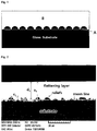
- Fig. 1 is a schematic cross-sectional view of a light emitting device with an internal light extraction layer according to the present invention, which comprises a random network of reliefs formed on a glass substrate from the first glass frit, and a flattening layer formed from the second glass frit on the network of reliefs.
- Fig. 2 is an SEM photograph of a cross-section of an internal light extraction layer actually formed according to the present invention. From Fig. 2 , we can plot the mean line of the roughness profile of the random network of reliefs, and measure the thickness of the flattening layer as the distance from this mean line to the top surface of the flattening layer.
- a relief has a height (b 1 ) of 3.1 ⁇ m, a width of 5.3 ⁇ m, and a pitch (c 1 ) (a distance between reliefs) of 10.6 ⁇ m, and a thickness of the flattening layer (d1) is 11.3 ⁇ m.
- a height (b) ranges from 1 to 10 ⁇ m, with the maximum height of said network being lower than 15 ⁇ m, and a width ranges from 2 to 40 ⁇ m, preferably at most 10 ⁇ m. Further, it is preferable that at least 50% (preferably at least 75%, and more preferably at least 85%) of pitches (c) of said network is in the range of 2 ⁇ m to 15 ⁇ m.
- An average total thickness (a') of the network and the flattening layer is from 6 ⁇ m to 20 ⁇ m.
- the ratio (r) of the height of the reliefs (b) to the pitch (c) of the reliefs, and the average total thickness (a') of the network and the flattening layer are within the range as described above, light scattering of a light incident from the lower part of the glass substrate is maximized by the uniform formation of the reliefs, thereby providing a homogeneous light extraction effect at the same time.
- the ratio (r) is preferably controlled to 0.5 or less in order to avoid merging between the agglomerates or reliefs.
- Fig. 3 schematically shows structural change of the first glass frit layer depending on the sintering temperature of the first glass frit.
- Fig. 3a shows the formation of porous glass frit structure wherein glass frit particles have not merged, when the first glass frit layer was sintered at a temperature lower than a temperature at which the network of reliefs can be formed.
- Fig. 3b shows the network of reliefs formed according to the present invention by sintering the first glass frit layer at an appropriate temperature at which the network of reliefs can be formed, to give partial agglomeration relief during sintering of the glass frit particles.
- Fig. 3c shows a densified structure in a continuous film shape with the glass frit particles completely sintered when the first glass frit layer was sintered at a temperature higher than a temperature at which reliefs can be formed.
- a composition of the first glass frit, a limited thickness of the first glass frit layer and an appropriate sintering temperature are critical. Based on the experimental results, it is preferable that a sintering temperature is about 60 to 110 °C higher than the glass transition temperature of the first glass frit. When said sintering temperature is too high, the first glass frit layer readily forms a densified structure. On the other hand, when said temperature is too low, the first glass frit layer forms a porous glass frit structure. If the first glass frit layer forms a porous glass frit structure as shown in Fig. 3a instead of the network of reliefs as shown in Fig. 3b , the optical transmittance deteriorates due to the porous glass frit structure.
- a small amount of voids may be formed inside the internal light extraction layer during the sintering process irrespective of the network of reliefs of the present invention. While this is inevitable during sintering of the glass frit layer, it is desirable that the voids are formed so as not to affect the total transmittance, absorbance, and haze ratio of a laminate for an light emitting device.
- the laminate for the light emitting device of the present invention can effectively extract light (which is lost at the interface) to the outside, maintain optical characteristics, such as the total transmittance and optical transmittance in a perpendicular direction, at a level similar to or better than an existing laminate for a light emitting device wherein a concavo-convex structures are formed on a substrate by using a patterning process after applying an additional layer.
- the laminate according to the invention is advantageous in that the preparation process is simple and convenient, the shape of the network of reliefs can be freely controlled, and the laminate can be prepared with a large area.
- the laminate for a light emitting device of the present invention may be used in a state where a transparent electrode layer (transparency given by the nature of material or by the arrangment in grid of metal absorbant and/or reflective like silver) is additionally stacked on the internal light extraction layer, when being applied to an optical device such as an OLED.
- a transparent electrode layer transmission given by the nature of material or by the arrangment in grid of metal absorbant and/or reflective like silver
- inorganic conductive materials such as transparent conductive oxide (TCO), for example, indium tin oxide (ITO), doped SnO 2 , indium zinc oxide (IZO), doped zinc oxide (ZnO) such as aluminium doped zinc oxide (AZO) or gallium doped zinc oxide (GZO) or graphene, or organic conductive materials, for example, polymeric material such as polyethylene dioxythiophene doped with polystyrene sulfonic acid (PSS) (PEDOT:PSS) or phthalocyanines such as copper phthalocyanine (CuPc) can be used.
- TCO transparent conductive oxide
- ITO indium tin oxide
- IZO indium zinc oxide
- ZnO doped zinc oxide
- AZO aluminium doped zinc oxide
- GZO gallium doped zinc oxide
- organic conductive materials for example, polymeric material such as polyethylene dioxythiophene doped with polystyrene sulfonic acid (PSS) (
- the metal grid can have a thickness of at least 100 nm and preferably at most 1500 nm.
- the grid can be formed from strands (also known as tracks) having a width A smaller than or equal to 50 ⁇ m and separated by an inter-strand distance B smaller than or equal to 5000 ⁇ m. These strands can be separated by a plurality of electrically insulated layers having a refractive index higher than 1.65, all covered by an electroconductive coating (inorganic materials such as transparent conductive oxide or organic materials, as described above).
- the strands are interconnected in the active zone of the OLED or (only) connected via their ends to electrical contacts.
- the grid may take the form of linear strands running parallel to one another and connected to electrical contacts through vias at their ends and/or may even take the form of closed patterns or meshes (strands interconnected to one another defining closed patterns), for example geometric (rectangular, square, polygonal, honeycomb, etc.) patterns of nonuniform shape and/or nonuniform size.
- the grid may contain a linear zone (strips of strands or tracks) and a zone containing closed patterns (meshed strands or tracks).
- the thickness may be smaller than 1500 nm, preferably less than 1000 nm, and especially from 100 nm to 1000 nm; or less than 800 nm, especially from 200 nm to 800 nm; or less than 650 nm.
- the width A can be chosen to be smaller than or equal to 50 ⁇ m in order to limit the visibility of the strands to the naked eye, and it can be chosen to be at least 100 nm in order to more easily obtain the objective of a low Rsquare.
- the width A can be smaller than 30 ⁇ m, and preferably from 1 to 20 ⁇ m and even more preferably from 1.5 to 20 ⁇ m or 1.5 to 15 ⁇ m.
- the inter-strand distance B may be at least 50 ⁇ m and even at least 200 ⁇ m and smaller than 5000 ⁇ m, preferably smaller than 2000 ⁇ m and even smaller than 1000 ⁇ m.
- Another feature of the metal grid is a coverage T which is smaller than 25% and preferably smaller than 10%, and even smaller than 6% or than 2%.
- the inter-strand distance B is between 2000 and 5000 ⁇ m when the thickness is between 800 and 1500 nm, and the width A is between 10 and 50 ⁇ m. This corresponds to a coverage of between 0.4 and 6.0%.
- the inter-strand distance B is between 200 and 1000 ⁇ m when the thickness is smaller than 500 nm, and the width A is between 3 and 20 ⁇ m or even from 3 to 10 ⁇ m. This corresponds to a coverage of between 0.5 and 22% or even from 0.5 to 11%.
- the metallic grid electrode disclosed in WO2014/135817 (A1 ) can be used.
- the metal grid can be formed by silvering.
- a conventional deposition method of the transparent electrode layer such as sputtering or deposition
- a conventional patterning method of the transparent electrode layer such as photolithography, etching or printing, may be used for preparing a transparent electrode pattern.
- a barrier layer which comprises silicon nitride, titanium oxide, aluminum oxide or the like, and preferably has a refractive index of 1.8 or more and a thickness of 200 nm or less, may be present between the internal light extraction layer and the electrode. Meanwhile, it is possible to increase light extraction efficiency and to protect the internal extraction layer from chemical etching through an additional process of depositing a SiO 2 , SiON, Si 3 N 4 , TiO 2 or Al 2 O 3 , or TiO 2 -Al 2 O 3 alloy barrier layer having a thickness of 5 to 50 nm on the internal light extraction layer.
- the barrier layer may comprise SiO 2 and/or Si 3 N 4 or an intermediate component called SiON.
- the barrier layer may comprise TiO 2 and/or Al 2 O 3 or an intermediate component such as TiO 2 -Al 2 O 3 alloy. Furthermore the barrier layer can be formed as a monolayer or as a multilayer (for example, alternating SiO 2 and Si 3 N 4 layers, or TiO 2 and Al 2 O 3 layers).
- Example 1 Preparation of a laminate for a light emitting device
- a sodalime glass substrate which has a thickness of 0.7 mm; a first glass frit paste comprising 20% by weight (based on the total weight of the paste) of glass frit which comprises 28.4% by weight of SiO 2 , 3.6% by weight of Al 2 O 3 , 39.5% by weight of B 2 O 3 , 11.6% by weight of ZnO, 3% by weight of P 2 O 5 and 13.9% by weight of Na 2 O (based on the total weight of the first glass frit paste), and 80% by weight (based on the total weight of the paste) of ethyl cellulose as a binder and butyl carbitol acetate as a solvent; and a second glass frit paste comprising 75% by weight (based on the total weight of the paste) of glass frit which comprises 70% by weight of Bi 2 O 3 , 10% by weight of ZnO, 3% by weight of Al 2 O 3 , 7% by weight of SiO 2 , 9% by weight of B 2 O 3 and 1% by weight of Na 2 O (based on
- the glass substrate was cleaned, and then the first glass frit paste was coated on the glass substrate by means of a screen printing method.
- the solvent was evaporated by drying the coated paste in an oven at 150 °C for about 20 minutes.
- ethyl cellulose contained in the dried paste was removed by keeping the dried paste in an oven at a temperature of 450 °C for about 20 minutes.
- the dried first glass frit layer was sintered at a temperature of 570 °C for about 10 minutes to form a random network of reliefs.
- the glass frit layer may be heated to remove ethyl cellulose and sintered by a successive process using a roll hearth furnace (RHF) or by using separate ovens.
- the network of reliefs prepared had a refractive index of 1.54 and a glass transition temperature of about 480 °C.
- Fig. 4 is a microphotograph of the random network of reliefs prepared as described above, which confirms the formation of the network of reliefs on the glass substrate by sintering of the first glass frit layer.
- the coverage of a random network of reliefs on the glass substrate, which can be calculated by optical image processing, is about 78% according to Fig. 4 .
- Fig. 5 shows SEM images of internal light extraction layers prepared according to Example 1, except with different sintering temperatures.
- Fig. 5a is an SEM image of an internal light extraction layer comprising porous first glass frit structures, in the case where the sintering temperature of the first glass frit layer is lower than 550 °C.
- Fig. 5b is an SEM image of an internal light extraction layer comprising a random network of reliefs made of the first glass frit, in the case where a sintering temperature of the first glass frit layer is 570 °C.
- Fig. 5c is an SEM image of an internal light extraction layer comprising a densified layer of the first glass frit, in the case where the sintering temperature of the first glass frit layer is 590 °C.
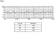
- Fig. 6 shows roughness profiles of the network of reliefs, which were measured using a cut-off filter having a profile filter ( ⁇ c ) of 0.08 mm and a profile filter ( ⁇ s ) of 0.08 ⁇ m.
- Ra arithmetical mean deviation of the roughness profile
- Ry maximum height of the roughness profile
- S mean spacing of local peaks
- the roughness profile was measured using the JIS B 0601:1994 standard.
- SURFCOM 1400D manufactured by Japan Tokyo Seimitsu Co., Ltd. was used for the measurement.
- the second glass frit paste was coated on the network of reliefs by means of a screen printing method.
- the solvent was evaporated by drying the coated paste in an oven at 150 °C for about 20 minutes.
- ethyl cellulose contained in the dried paste was removed by keeping the dried paste in an oven at a temperature of 150 °C for about 10 minutes.
- the dried second glass frit layer was sintered at a temperature of 545 °C in an IR furnace for about 10 minutes to form a flattening layer.
- the glass frit layer may be heated to remove ethyl cellulose and sintered by a successive process using a roll hearth furnace (RHF) or using separate ovens.
- the flattening layer prepared had a refractive index of about 1.9.
- the roughness profile of the network of reliefs once covered by the flattening layer could be analyzed through a SEM cross-section-image-analysis between the network of reliefs and the flattening layer.
- Comparative Example 1 Preparation of a laminate for a light emitting device
- An internal light extraction layer was formed according to the procedure of Example 1, except that porous glass frit structures were formed at a lower sintering temperature (i.e., a temperature not more than 550 °C) ( Fig. 5a ).
- Comparative Example 2 Preparation of a laminate for a light emitting device
- An internal light extraction layer was formed according to the procedure of Example 1, except that the first glass frit was flattened by sintering at a higher sintering temperature (i.e., a temperature of 590 °C or more) ( Fig. 5c ).
- a sintering temperature T1 of the first glass frit layer was not more than 550 °C ( Fig. 5a )
- bubbles were generated in a large amount, and reliefs were not formed.
- a sintering temperature T1 of the first glass frit layer was not less than 590 °C ( Fig. 5c )
- the reliefs were deformed to become flat.
- the sintering temperature T1 of the first glass frit layer was within a range from 550 to 590 °C, preferably from 560 to 580 °C ( Fig. 5b )
- bubbling inside the first glass frit layer was inhibited, and the intended reliefs were obtained.
- a laminate for a light emitting device having reliefs with a stable shape were maintained during the sintering process of the flattening layer.
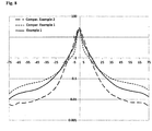
- Example 1 An internal light extraction layer was formed according to the procedure of Example 1, except that the thickness of the flattening layer was increased to 30 ⁇ m or more. Table 1.
- the result of total luminous transmittance (%) was measured by ASTM D 1003 for laminates for the light emitting device of Example 1, Comparative Example 1 and Comparative Example 3. Standard for measurement: ASTM D 1003
- Example 1 Comp. Example 1 Comp.
- Example 3 Total Thickness ( ⁇ m) 13.1 11.3 47.6 Total Luminous Transmittance (%) 73.1 64.1 63.5 Percent Haze (%) 72.8 83.7 82.0
- Comparative Example 3 had a thicker flattening layer compared to Example 1. Even though the reliefs of Example 1 and Comparative Example 3 had similar average thicknesses, the results in Comparative Example 3 was poor due to increase of light loss, which occurs by the increased light paths as the thickness of the flattening layer increases.
- Example 1 The total luminous transmittance of Example 1 was the highest among the three samples.
- Fig. 7 shows SEM photographs of an internal light extraction layer prepared according to the procedure of Example 1 ( Fig. 7a ) and Comparative Example 3 ( Fig. 7b ).
- Fig. 7b many air bubbles exist inside the flattening layer generated during the sintering process.
- the concentration of captured air bubbles increases according to the increase of the thickness of the flattening layer.
- the air bubbles also lead to reduction of total luminerous transmittance due to an increase of light path.
- the thickness of the second glass frit paste layer increases, the process time for forming (sintering) the flattening layer increases, which is economically disadvantages.
- Fig. 8 is a graph showing the intensity distribution of externally emitted light with respect to a viewing angle.
- GONIOPHOTOMETER GP-11R manufactured by Murakami Color Research Laboratory Co. was used for the measurement.
- the laminate for a light emitting device according to the present invention (Example 1) exhibits good intensity as compared to that of Comparative Example 1 at a viewing angle between -20° and 20°, since the laminate according to the invention can form many prominent structures. Further, the laminate of Example 1 exhibits good intensity as compared to that of Comparative Example 3 at a viewing angle between -20° and 20°, since the laminate according to the invention has excellent light diffusive performance.
- the laminate for a light emitting device according to the present invention which comprises a random network of reliefs of low refractive index advantageously exhibits excellent light diffusive performance and superior optical transmittance in a perpendicular direction.
- a laminate for a light emitting device of the present invention can be widely used for light emitting devices requiring efficient extraction of light, being particularly suitable in the industrial fields of optical devices, such as organic light emitting diodes (OLEDs), backlights, and lighting, due to its superior optical characteristics.
- OLEDs organic light emitting diodes
Landscapes
- Physics & Mathematics (AREA)
- Optics & Photonics (AREA)
- Engineering & Computer Science (AREA)
- General Engineering & Computer Science (AREA)
- Chemical & Material Sciences (AREA)
- Microelectronics & Electronic Packaging (AREA)
- Materials Engineering (AREA)
- Organic Chemistry (AREA)
- Manufacturing & Machinery (AREA)
- Electroluminescent Light Sources (AREA)
- Glass Compositions (AREA)
Claims (28)
- Laminat für eine lichtemittierende Vorrichtung, umfassend:ein Glassubstrat mit einem Brechungsindex n1 von 1,45 bis 1,65;ein zufälliges Netzwerk von Reliefs aus Email, das auf dem Glassubstrat ausgebildet ist, wobei das Netzwerk einen Brechungsindex n2 im Bereich von 1,45 bis 1,65 aufweist; undeine Glättungsschicht aus Email, die auf dem Netzwerk und dem Glassubstrat ausgebildet ist, wobei die Glättungsschicht einen Brechungsindex n3 im Bereich von 1,8 bis 2,1 aufweist;dadurch gekennzeichnet, dass
mindestens 50 %, vorzugsweise mindestens 75 % und stärker bevorzugt mindestens 85 % der Reliefs einen Querschnitt zeigen, der Folgendes aufweist:eine Höhe (b) im Bereich von 1 bis 10 µm, wobei die maximale Höhe der Reliefs vorzugsweise geringer als 15 µm ist, undeine Breite im Bereich von 2 bis 40 µm, vorzugsweise höchstens 10 µm; undwobei mindestens 50 %, vorzugsweise mindestens 75 % und stärker bevorzugt mindestens 85 % der Teilungsabstände (c) des Netzwerks im Bereich von 2 µm bis 15 µm liegen, wobei ein Teilungsabstand der Abstand von dem Mittelpunkt des untersten Teils eines Reliefs zu dem Mittelpunkt des untersten Teils eines anderen, benachbarten Reliefs ist. - Laminat nach Anspruch 1, worin das Netzwerk ein Rauigkeitsprofil mit Ra, die arithmetische Mittelwertabweichung des Rauigkeitsprofils, im Bereich von 0,3 µm bis 3 µm, vorzugsweise 0,3 µm bis 1 µm; mit Ry, die maximale Höhe des Rauigkeitsprofils im Bereich von 1 µm bis 10 µm; und S, die mittlere Beabstandung lokaler Peaks, im Bereich von 2 µm bis 40 µm, vorzugsweise 2 bis 20 µm, zeigt.
- Laminat nach Anspruch 1 oder 2, worin ein Verhältnis (r) einer durchschnittlichen Höhe (b') der Reliefs zu einem durchschnittlichen Teilungsabstand (c') der Reliefs 0,1 bis 0,5 beträgt.
- Laminat nach einem der Ansprüche 1 bis 3, worin der Anteil der Fläche, auf der das Netzwerk das Glassubstrat bedeckt, 60 bis 90 % beträgt.
- Laminat nach einem der Ansprüche 1 bis 4, worin die Reliefs Hügel und/oder Ansammlungen von Hügeln umfassen.
- Laminat nach einem der Ansprüche 1 bis 5, worin die durchschnittliche Gesamtdicke (a') des Netzwerks und der Glättungsschicht im Bereich von 6 bis 20 µm liegt.
- Laminat nach einem der Ansprüche 1 bis 6, worin die Dicke der Glättungsschicht (d) weniger als 20 µm beträgt.
- Laminat nach einem der Ansprüche 1 bis 7, worin die Rauigkeit Ra, gemessen an der Oberfläche der Glättungsschicht, nicht mehr als 1 nm beträgt.
- Laminat nach einem der Ansprüche 1 bis 8, worin das Netzwerk aus einer ersten Glasfritte gebildet ist und die erste Glasfritte 10 bis 40 Gew.-% SiO2, 1 bis 7 Gew.-% Al2O3, 0 bis 10 Gew.-% P2O5, 20 bis 50 Gew.-% B2O3, 3 bis 35 Gew.-% ZnO und 5 bis 20 Gew.-% mindestens eines Alkalimetalloxids, ausgewählt aus der Gruppe bestehend aus Na2O, Li2O und K2O, bezogen auf das Gesamtgewicht der ersten Glasfritte nach der Ausbildung des Netzwerks, umfasst.
- Laminat nach einem der Ansprüche 1 bis 9, worin die Glättungsschicht aus einer zweiten Glasfritte ausgebildet ist und die zweite Glasfritte 55 bis 84 Gew.-% Bi2O3, 0 bis 20 Gew.-% BaO, 5 bis 20 Gew.-% ZnO, 1 bis 7 Gew.-% Al2O3, 5 bis 15 Gew.-% SiO2, 5 bis 20 Gew.-% B2O3, 0 bis 0,1 Gew.-% CeO2, 0,05 bis 5 Gew.-% Na2O und weniger als 5 Gew.-% einer oder mehrerer Verbindungen, ausgewählt aus der Gruppe bestehend aus TiO2, ZrO2, La2O3, Nb2O3 und MgO, bezogen auf das Gesamtgewicht der zweiten Glasfritte nach der Ausbildung der Glättungsschicht, umfasst.
- Laminat nach einem der Ansprüche 1 bis 10, worin das Glassubstrat ein Natronkalkglassubstrat ist.
- Laminat nach einem der Ansprüche 1 bis 11, worin das Laminat ein Trübungsverhältnis von mindestens 70 % und eine Gesamtlichtdurchlässigkeit von mindestens 65 % zeigt.
- Laminat nach einem der Ansprüche 1 bis 12, weiter umfassend eine transparente Elektrode auf der Glättungsschicht.
- Lichtemittierende Vorrichtung, umfassend das Laminat nach einem der Ansprüche 1 bis 13.
- Verfahren zur Herstellung eines Laminats für eine lichtemittierende Vorrichtung, umfassend die folgenden Schritte:(a) Bereitstellen eines Glassubstrats mit einem Brechungsindex n1 von 1,45 bis 1,65;(b-1) Ausbilden einer ersten Glasfrittenpastenschicht durch Aufbringen einer ersten Glasfrittenpaste, die ein organisches Lösungsmittel und ein erstes Glasfrittenpulver umfasst, auf dem Glassubstrat, wobei das erste Glasfrittenpulver in einer Menge von 50 Gew.-% oder weniger, bezogen auf das Gesamtgewicht der ersten Glasfrittenpaste, enthalten ist und die erste Pastenschicht eine gegebene Fläche des Glassubstrats bedeckt;(b-2) Entfernen des organischen Lösungsmittels durch Trocknen der aufgebrachten ersten Glasfrittenpastenschicht;(b-3) Ausbilden eines zufälligen Netzwerks von Reliefs durch Sintern der getrockneten ersten Glasfrittenschicht bei einer Sintertemperatur T1, um eine teilweise Agglomeration oder Verdichtung des ersten Glasfrittenpulvers zu bewirken;(c-1) Ausbilden einer zweiten Glasfrittenpastenschicht durch Aufbringen einer zweiten Glasfrittenpaste, die ein organisches Lösungsmittel und ein zweites Glasfrittenpulver umfasst, auf das Netzwerk;(c-2) Entfernen des organischen Lösungsmittels durch Trocknen der aufgebrachten zweiten Glasfrittenschicht; und(c-3) Ausbilden einer Glättungsschicht durch Sintern der getrockneten zweiten Glasfrittenschicht bei einer Sintertemperatur T2;wobei mindestens 50 %, vorzugsweise mindestens 75 % und stärker bevorzugt mindestens 85 % der Reliefs einen Querschnitt zeigen, der Folgendes aufweist: eine Höhe (b) im Bereich von 1 bis 10 µm, wobei die maximale Höhe der Reliefs vorzugsweise nicht höher als 15 µm ist, und
eine Breite im Bereich von 2 bis 40 µm, vorzugsweise höchstens 10 µm; und
wobei mindestens 50 %, vorzugsweise mindestens 75 %, stärker bevorzugt mindestens 85 %, der Teilungsabstände (c) des Netzwerks im Bereich von 2 µm bis 15 µm liegen, wobei ein Teilungsabstand der Abstand von dem Mittelpunkt des untersten Teils eines Reliefs zu dem Mittelpunkt des untersten Teils eines anderen, angrenzenden Reliefs ist. - Verfahren nach Anspruch 15, worin das erste Glasfrittenpulver in einer Menge von 10 bis 50 Gew.-%, bezogen auf das Gesamtgewicht der ersten Glasfrittenpaste, enthalten ist.
- Verfahren nach Anspruch 15 oder 16, worin die Sintertemperatur T1 in Schritt (b-3) 60 bis 110 °C höher ist als die Glasübergangstemperatur der ersten Glasfritte.
- Verfahren nach einem der Ansprüche 15 bis 17, worin die Sintertemperatur T1 in Schritt (b-3) im Bereich von 550 bis 590 °C liegt und die Sintertemperatur T2 in Schritt (c-3) vorzugsweise gleich hoch wie T1 oder niedriger ist.
- Verfahren nach einem der Ansprüche 15 bis 18, worin an den Schritten (b-1) bis (b-3) kein zusätzlicher Strukturierungsprozess wie Lithografie oder Prägung beteiligt ist.
- Verfahren nach einem der Ansprüche 15 bis 19, worin das Verhältnis (r) der durchschnittlichen Höhe (b') der Reliefs zu dem durchschnittlichen Teilungsabstand (c') der Reliefs 0,1 bis 0,5 beträgt.
- Verfahren nach einem der Ansprüche 15 bis 20, worin die durchschnittliche Gesamtdicke (a') des Netzwerks und der Glättungsschicht im Bereich von 6 bis 20 µm liegt.
- Verfahren nach einem der Ansprüche 15 bis 21, worin die Dicke der Glättungsschicht (d) weniger als 20 µm beträgt.
- Verfahren nach einem der Ansprüche 15 bis 22, wobei das erste Glasfrittenpulver 10 bis 40 Gew.-% SiO2, 1 bis 7 Gew.-% Al2O3, 0 bis 10 Gew.-% P2O5, 20 bis 50 Gew.-% B2O3, 3 bis 35 Gew.-% ZnO und 5 bis 20 Gew.-% mindestens eines Alkalimetalloxids, ausgewählt aus der Gruppe bestehend aus Na2O, Li2O und K2O, bezogen auf das Gesamtgewicht der ersten Glasfritte nach Ausbildung des Netzwerks, umfasst.
- Verfahren nach einem der Ansprüche 15 bis 23, wobei das zweite Glasfrittenpulver 55 bis 84 Gew.-% Bi2O3, 0 bis 20 Gew.-% BaO, 5 bis 20 Gew.-% ZnO, 1 bis 7 Gew.-% Al2O3, 5 bis 15 Gew.-% SiO2, 5 bis 20 Gew.-% B2O3, 0 bis 0,1 Gew.-% CeO2, 0,05 bis 5 Gew.-% Na2O und weniger als 5 Gew.-% einer oder mehrerer Verbindungen, ausgewählt aus der Gruppe bestehend aus TiO2, ZrO2, La2O3, Nb2O3 und MgO, bezogen auf das Gesamtgewicht der zweiten Glasfritte nach Ausbildung der Glättungsschicht, umfasst.
- Verfahren nach einem der Ansprüche 15 bis 24, wobei das Glassubstrat ein Natronkalkglassubstrat ist.
- Laminat nach einem der Ansprüche 1 bis 13, wobei die Glättungsschicht weiter Hohlräume umfasst.
- Laminat nach Anspruch 13, wobei die transparente Elektrode ausgewählt ist aus der Gruppe bestehend aus anorganischen leitfähigen Materialien wie Indiumzinnoxid (ITO), dotiertem SnO2, Indiumzinkoxid (IZO), dotiertem Zinkoxid (ZnO) wie mit Aluminium dotiertem Zinkoxid (AZO) oder mit Gallium dotiertem Zinkoxid (GZO) und Graphen und organischen leitfähigen Materialien wie mit Polystyrolsulfonsäure (PSS) dotiertem Polyethylendioxythiophen (PEDOT:PSS) und Phthalocyaninen wie Kupferphthalocyanin (CuPc), wobei die transparente Elektrode ein Metallgitter, vorzugsweise ein Silbergitter, umfassen kann.
- Laminat nach Anspruch 13 oder 27, weiter umfassend eine Sperrschicht, die eine oder mehrere Schichten, ausgewählt aus der Gruppe bestehend aus einer SiO2-Schicht, einer SiON-Schicht, einer Si3N4-Schicht, einer TiO2-Schicht, einer Al2O3-Schicht und einer TiO2-Al2O3-Legierungsschicht, zwischen der Glättungsschicht und der Elektrode umfasst.
Applications Claiming Priority (2)
| Application Number | Priority Date | Filing Date | Title |
|---|---|---|---|
| KR20130119830A KR101493612B1 (ko) | 2013-10-08 | 2013-10-08 | 발광 디바이스용 적층체 및 그의 제조 방법 |
| PCT/KR2014/009420 WO2015053529A1 (en) | 2013-10-08 | 2014-10-07 | Laminate for light emitting device and process of preparing same |
Publications (3)
| Publication Number | Publication Date |
|---|---|
| EP3055892A1 EP3055892A1 (de) | 2016-08-17 |
| EP3055892A4 EP3055892A4 (de) | 2017-05-17 |
| EP3055892B1 true EP3055892B1 (de) | 2018-07-18 |
Family
ID=52593500
Family Applications (1)
| Application Number | Title | Priority Date | Filing Date |
|---|---|---|---|
| EP14851475.5A Not-in-force EP3055892B1 (de) | 2013-10-08 | 2014-10-07 | Laminat für eine lichtemittierende vorrichtung und verfahren zur herstellung davon |
Country Status (9)
| Country | Link |
|---|---|
| US (1) | US9634290B2 (de) |
| EP (1) | EP3055892B1 (de) |
| JP (1) | JP6630269B2 (de) |
| KR (1) | KR101493612B1 (de) |
| CN (1) | CN105684181B (de) |
| ES (1) | ES2690404T3 (de) |
| RU (1) | RU2663086C2 (de) |
| TW (1) | TWI555253B (de) |
| WO (1) | WO2015053529A1 (de) |
Families Citing this family (9)
| Publication number | Priority date | Publication date | Assignee | Title |
|---|---|---|---|---|
| KR101493601B1 (ko) * | 2013-07-17 | 2015-02-13 | 쌩-고벵 글래스 프랑스 | 발광 디바이스용 적층체 및 그의 제조 방법 |
| JP2018067414A (ja) * | 2016-10-18 | 2018-04-26 | OLED Material Solutions株式会社 | 電子デバイス用基板のマザー基板 |
| WO2018102512A1 (en) * | 2016-11-30 | 2018-06-07 | Corning Incorporated | Textured glass for light extraction enhancement of oled lighting |
| KR20220123557A (ko) * | 2017-02-20 | 2022-09-07 | 카티바, 인크. | 향상된 광 아웃커플링을 갖는 발광 소자를 위한 잉크젯 인쇄 시스템 및 기술 |
| FR3074167B1 (fr) * | 2017-11-30 | 2019-11-15 | Saint-Gobain Glass France | Feuille de verre revetue d'un empilement de couches minces et d'une couche d'email. |
| CN108512029B (zh) * | 2018-04-16 | 2020-03-24 | 齐鲁工业大学 | 一种基于非晶铋酸盐的超宽带随机激光散射材料、激光器件及制备与应用 |
| CN109461826B (zh) * | 2018-08-29 | 2020-08-14 | 云谷(固安)科技有限公司 | 一种显示面板和显示装置 |
| KR102799116B1 (ko) * | 2019-07-01 | 2025-04-21 | 쇼오트 글라스 테크놀로지스 (쑤저우) 코퍼레이션 리미티드. | 회절 광학 소자 및 회절 광학 소자의 제조 방법 |
| KR102715988B1 (ko) | 2019-09-06 | 2024-10-11 | 쇼오트 글라스 테크놀로지스 (쑤저우) 코퍼레이션 리미티드. | 유리 기판과 미세구조 층 사이의 높은 결합 강도를 갖는 미세 광학 소자 |
Family Cites Families (39)
| Publication number | Priority date | Publication date | Assignee | Title |
|---|---|---|---|---|
| US5309070A (en) | 1991-03-12 | 1994-05-03 | Sun Sey Shing | AC TFEL device having blue light emitting thiogallate phosphor |
| JPH07155598A (ja) | 1993-12-10 | 1995-06-20 | Toto Ltd | 光触媒被膜及び光触媒被膜の形成方法 |
| ATE166858T1 (de) | 1994-10-13 | 1998-06-15 | Saint Gobain Vitrage | Substrat aus verstärktem glas |
| DE69604359T2 (de) | 1995-11-03 | 2000-03-30 | Quest International B.V., Naarden | Cyclopentylidene-cyclopentanol in Parfümerie |
| ZA973692B (en) * | 1996-05-17 | 1997-11-25 | Dexter Corp | Extrusion coating compositions and method. |
| FR2757150B1 (fr) | 1996-12-12 | 1999-01-22 | Saint Gobain Vitrage | Procede d'emaillage de substrats en verre, composition d'email utilisee et produits obtenus |
| ES2181196T3 (es) | 1997-03-13 | 2003-02-16 | Saint Gobain | Composiciones de vidrio silico-sodo-calcicas y sus aplicaciones. |
| AU4157202A (en) * | 2000-10-24 | 2002-05-27 | Ppg Ind Ohio Inc | Method of making coated articles and coated articles made thereby |
| EP1330844A1 (de) | 2000-11-02 | 2003-07-30 | 3M Innovative Properties Company | Helligkeits- und kontraststeigerung von direktsicht-emissionsanzeigevorrichtungen |
| JP2007287486A (ja) * | 2006-04-17 | 2007-11-01 | Aitesu:Kk | 透明基板と電極の間に微細構造体を有する有機el素子 |
| KR101548025B1 (ko) | 2007-07-27 | 2015-08-27 | 아사히 가라스 가부시키가이샤 | 투광성 기판, 그의 제조 방법, 유기 led 소자 및 그의 제조 방법 |
| JPWO2009060916A1 (ja) | 2007-11-09 | 2011-03-24 | 旭硝子株式会社 | 透光性基板、その製造方法、有機led素子およびその製造方法 |
| FR2924274B1 (fr) * | 2007-11-22 | 2012-11-30 | Saint Gobain | Substrat porteur d'une electrode, dispositif electroluminescent organique l'incorporant, et sa fabrication |
| WO2009116531A1 (ja) | 2008-03-18 | 2009-09-24 | 旭硝子株式会社 | 電子デバイス用基板、有機led素子用積層体及びその製造方法、有機led素子及びその製造方法 |
| US20100110551A1 (en) * | 2008-10-31 | 2010-05-06 | 3M Innovative Properties Company | Light extraction film with high index backfill layer and passivation layer |
| WO2010058755A1 (ja) | 2008-11-18 | 2010-05-27 | 株式会社クラレ | 面光源素子およびそれを用いた画像表示装置ならびに照明装置 |
| US7957621B2 (en) | 2008-12-17 | 2011-06-07 | 3M Innovative Properties Company | Light extraction film with nanoparticle coatings |
| WO2010084922A1 (ja) | 2009-01-26 | 2010-07-29 | 旭硝子株式会社 | 有機led素子の散乱層用ガラス及び有機led素子 |
| CN102293054B (zh) | 2009-01-26 | 2016-08-03 | 旭硝子株式会社 | 电子器件用基板及使用该基板的电子器件 |
| JP5541165B2 (ja) | 2009-01-26 | 2014-07-09 | 旭硝子株式会社 | 電子デバイス用基板の製造方法、電子デバイスの製造方法、電子デバイス用基板、および電子デバイス |
| KR20100131074A (ko) * | 2009-06-05 | 2010-12-15 | 엘지디스플레이 주식회사 | 상부 발광방식 유기전계발광소자 및 이의 제조방법 |
| FR2963705B1 (fr) * | 2010-08-06 | 2012-08-17 | Saint Gobain | Support a couche diffusante pour dispositif a diode electroluminescente organique, dispositif electroluminescent organique comportant un tel support |
| FR2964254B1 (fr) * | 2010-08-30 | 2013-06-14 | Saint Gobain | Support de dispositif a diode electroluminescente organique, un tel dispositif a diode electroluminescente organique et son procede de fabrication |
| CN103097098B (zh) * | 2010-09-30 | 2015-11-25 | 三菱丽阳株式会社 | 表面具有微细凹凸构造的模具、表面具有微细凹凸构造的物品制造方法、物品用途、体现色彩差异的层积体以及面发光体 |
| KR101638488B1 (ko) | 2010-12-08 | 2016-07-11 | 니폰 덴키 가라스 가부시키가이샤 | 고굴절률 유리 |
| KR101863948B1 (ko) | 2010-12-20 | 2018-07-04 | 삼성전자주식회사 | 발광 소자 기판과 그 제조 방법, 면발광 소자, 조명 기구 및 백라이트 |
| JP5938757B2 (ja) | 2011-11-25 | 2016-06-22 | 三星電子株式会社Samsung Electronics Co.,Ltd. | 発光素子基板とその製造方法、面発光素子、照明器具およびバックライト |
| US9224983B2 (en) | 2010-12-20 | 2015-12-29 | Samsung Electronics Co., Ltd. | Substrate for surface light emitting device and method of manufacturing the substrate, surface light emitting device, lighting apparatus, and backlight including the same |
| WO2012086396A1 (ja) | 2010-12-20 | 2012-06-28 | 旭硝子株式会社 | 有機el素子および透光性基板 |
| JP4952842B2 (ja) * | 2010-12-24 | 2012-06-13 | 大日本印刷株式会社 | 色変換層形成用塗工液および有機エレクトロルミネッセンス素子用基板、ならびにこれらの製造方法 |
| US8692446B2 (en) | 2011-03-17 | 2014-04-08 | 3M Innovative Properties Company | OLED light extraction films having nanoparticles and periodic structures |
| US9882170B2 (en) * | 2011-05-25 | 2018-01-30 | Koninklijke Philips N.V. | Organic light emitting device with improved light extraction |
| WO2013008982A1 (ko) | 2011-07-14 | 2013-01-17 | 엘티씨 (주) | 높은 광추출 성능을 갖는 무기 산란막 {inorganic scattering films having high light extraction performance} |
| JP2013025900A (ja) | 2011-07-15 | 2013-02-04 | Asahi Glass Co Ltd | 電子デバイス用基板、及び、これを用いた有機led素子 |
| JP2013109922A (ja) * | 2011-11-18 | 2013-06-06 | Asahi Glass Co Ltd | 電子デバイス用基板、及び、これを用いた有機led |
| DE102012200084B4 (de) | 2012-01-04 | 2021-05-12 | Pictiva Displays International Limited | Strahlungsemittierendes organisches bauteil |
| CN103000817B (zh) | 2012-11-29 | 2016-04-20 | 无锡格菲电子薄膜科技有限公司 | 一种柔性有机发光二极管 |
| FR3003084B1 (fr) | 2013-03-08 | 2015-02-27 | Saint Gobain | Support electroconducteur pour oled, oled l'incorporant, et sa fabrication |
| KR101493601B1 (ko) * | 2013-07-17 | 2015-02-13 | 쌩-고벵 글래스 프랑스 | 발광 디바이스용 적층체 및 그의 제조 방법 |
-
2013
- 2013-10-08 KR KR20130119830A patent/KR101493612B1/ko not_active Expired - Fee Related
-
2014
- 2014-10-07 CN CN201480054890.2A patent/CN105684181B/zh not_active Expired - Fee Related
- 2014-10-07 US US15/027,383 patent/US9634290B2/en not_active Expired - Fee Related
- 2014-10-07 TW TW103134930A patent/TWI555253B/zh not_active IP Right Cessation
- 2014-10-07 ES ES14851475.5T patent/ES2690404T3/es active Active
- 2014-10-07 RU RU2016117270A patent/RU2663086C2/ru active
- 2014-10-07 WO PCT/KR2014/009420 patent/WO2015053529A1/en not_active Ceased
- 2014-10-07 EP EP14851475.5A patent/EP3055892B1/de not_active Not-in-force
- 2014-10-07 JP JP2016520628A patent/JP6630269B2/ja not_active Expired - Fee Related
Non-Patent Citations (1)
| Title |
|---|
| None * |
Also Published As
| Publication number | Publication date |
|---|---|
| US9634290B2 (en) | 2017-04-25 |
| RU2016117270A3 (de) | 2018-05-28 |
| CN105684181B (zh) | 2018-03-27 |
| JP2016532994A (ja) | 2016-10-20 |
| WO2015053529A1 (en) | 2015-04-16 |
| RU2016117270A (ru) | 2017-11-15 |
| RU2663086C2 (ru) | 2018-08-01 |
| KR101493612B1 (ko) | 2015-02-13 |
| CN105684181A (zh) | 2016-06-15 |
| US20160248047A1 (en) | 2016-08-25 |
| JP6630269B2 (ja) | 2020-01-15 |
| TWI555253B (zh) | 2016-10-21 |
| TW201523959A (zh) | 2015-06-16 |
| EP3055892A1 (de) | 2016-08-17 |
| EP3055892A4 (de) | 2017-05-17 |
| ES2690404T3 (es) | 2018-11-20 |
Similar Documents
| Publication | Publication Date | Title |
|---|---|---|
| EP3055892B1 (de) | Laminat für eine lichtemittierende vorrichtung und verfahren zur herstellung davon | |
| EP2384086B1 (de) | Substrat für ein elektronisches gerät und elektronisches gerät damit | |
| KR101493601B1 (ko) | 발광 디바이스용 적층체 및 그의 제조 방법 | |
| EP2862212B1 (de) | Schichtstruktur für oled-vorrichtung und oled-vorrichtung damit | |
| CN105140415A (zh) | 具有电极的基材、与其结合的有机发光装置、及其制造 | |
| TWI577068B (zh) | 發光器件及增加具有玻璃基板之器件之光散射的方法 | |
| KR20130106832A (ko) | 유기 발광 다이오드 소자의 지지체, 이러한 유기 발광 다이오드 소자 및 그의 제조 방법 | |
| KR101823358B1 (ko) | 투광성 기판의 제조방법 및 이를 통해 제조된 투광성 기판 | |
| KR101862760B1 (ko) | 투광성 기판의 제조방법 및 이를 통해 제조된 투광성 기판 | |
| KR101862763B1 (ko) | 투광성 기판 및 이의 제조방법 |
Legal Events
| Date | Code | Title | Description |
|---|---|---|---|
| PUAI | Public reference made under article 153(3) epc to a published international application that has entered the european phase |
Free format text: ORIGINAL CODE: 0009012 |
|
| 17P | Request for examination filed |
Effective date: 20160509 |
|
| AK | Designated contracting states |
Kind code of ref document: A1 Designated state(s): AL AT BE BG CH CY CZ DE DK EE ES FI FR GB GR HR HU IE IS IT LI LT LU LV MC MK MT NL NO PL PT RO RS SE SI SK SM TR |
|
| AX | Request for extension of the european patent |
Extension state: BA ME |
|
| DAX | Request for extension of the european patent (deleted) | ||
| A4 | Supplementary search report drawn up and despatched |
Effective date: 20170421 |
|
| RIC1 | Information provided on ipc code assigned before grant |
Ipc: H01L 51/56 20060101ALI20170413BHEP Ipc: H01L 51/52 20060101AFI20170413BHEP |
|
| GRAP | Despatch of communication of intention to grant a patent |
Free format text: ORIGINAL CODE: EPIDOSNIGR1 |
|
| INTG | Intention to grant announced |
Effective date: 20180215 |
|
| GRAS | Grant fee paid |
Free format text: ORIGINAL CODE: EPIDOSNIGR3 |
|
| GRAA | (expected) grant |
Free format text: ORIGINAL CODE: 0009210 |
|
| AK | Designated contracting states |
Kind code of ref document: B1 Designated state(s): AL AT BE BG CH CY CZ DE DK EE ES FI FR GB GR HR HU IE IS IT LI LT LU LV MC MK MT NL NO PL PT RO RS SE SI SK SM TR |
|
| REG | Reference to a national code |
Ref country code: GB Ref legal event code: FG4D |
|
| REG | Reference to a national code |
Ref country code: CH Ref legal event code: EP |
|
| REG | Reference to a national code |
Ref country code: IE Ref legal event code: FG4D |
|
| REG | Reference to a national code |
Ref country code: AT Ref legal event code: REF Ref document number: 1020296 Country of ref document: AT Kind code of ref document: T Effective date: 20180815 |
|
| REG | Reference to a national code |
Ref country code: DE Ref legal event code: R096 Ref document number: 602014028900 Country of ref document: DE |
|
| REG | Reference to a national code |
Ref country code: FR Ref legal event code: PLFP Year of fee payment: 5 |
|
| REG | Reference to a national code |
Ref country code: CH Ref legal event code: NV Representative=s name: DENNEMEYER AG, CH Ref country code: NL Ref legal event code: FP |
|
| REG | Reference to a national code |
Ref country code: ES Ref legal event code: FG2A Ref document number: 2690404 Country of ref document: ES Kind code of ref document: T3 Effective date: 20181120 |
|
| REG | Reference to a national code |
Ref country code: LT Ref legal event code: MG4D |
|
| PG25 | Lapsed in a contracting state [announced via postgrant information from national office to epo] |
Ref country code: GR Free format text: LAPSE BECAUSE OF FAILURE TO SUBMIT A TRANSLATION OF THE DESCRIPTION OR TO PAY THE FEE WITHIN THE PRESCRIBED TIME-LIMIT Effective date: 20181019 Ref country code: NO Free format text: LAPSE BECAUSE OF FAILURE TO SUBMIT A TRANSLATION OF THE DESCRIPTION OR TO PAY THE FEE WITHIN THE PRESCRIBED TIME-LIMIT Effective date: 20181018 Ref country code: SE Free format text: LAPSE BECAUSE OF FAILURE TO SUBMIT A TRANSLATION OF THE DESCRIPTION OR TO PAY THE FEE WITHIN THE PRESCRIBED TIME-LIMIT Effective date: 20180718 Ref country code: BG Free format text: LAPSE BECAUSE OF FAILURE TO SUBMIT A TRANSLATION OF THE DESCRIPTION OR TO PAY THE FEE WITHIN THE PRESCRIBED TIME-LIMIT Effective date: 20181018 Ref country code: RS Free format text: LAPSE BECAUSE OF FAILURE TO SUBMIT A TRANSLATION OF THE DESCRIPTION OR TO PAY THE FEE WITHIN THE PRESCRIBED TIME-LIMIT Effective date: 20180718 Ref country code: PL Free format text: LAPSE BECAUSE OF FAILURE TO SUBMIT A TRANSLATION OF THE DESCRIPTION OR TO PAY THE FEE WITHIN THE PRESCRIBED TIME-LIMIT Effective date: 20180718 Ref country code: FI Free format text: LAPSE BECAUSE OF FAILURE TO SUBMIT A TRANSLATION OF THE DESCRIPTION OR TO PAY THE FEE WITHIN THE PRESCRIBED TIME-LIMIT Effective date: 20180718 Ref country code: LT Free format text: LAPSE BECAUSE OF FAILURE TO SUBMIT A TRANSLATION OF THE DESCRIPTION OR TO PAY THE FEE WITHIN THE PRESCRIBED TIME-LIMIT Effective date: 20180718 Ref country code: IS Free format text: LAPSE BECAUSE OF FAILURE TO SUBMIT A TRANSLATION OF THE DESCRIPTION OR TO PAY THE FEE WITHIN THE PRESCRIBED TIME-LIMIT Effective date: 20181118 |
|
| PG25 | Lapsed in a contracting state [announced via postgrant information from national office to epo] |
Ref country code: AL Free format text: LAPSE BECAUSE OF FAILURE TO SUBMIT A TRANSLATION OF THE DESCRIPTION OR TO PAY THE FEE WITHIN THE PRESCRIBED TIME-LIMIT Effective date: 20180718 Ref country code: LV Free format text: LAPSE BECAUSE OF FAILURE TO SUBMIT A TRANSLATION OF THE DESCRIPTION OR TO PAY THE FEE WITHIN THE PRESCRIBED TIME-LIMIT Effective date: 20180718 Ref country code: HR Free format text: LAPSE BECAUSE OF FAILURE TO SUBMIT A TRANSLATION OF THE DESCRIPTION OR TO PAY THE FEE WITHIN THE PRESCRIBED TIME-LIMIT Effective date: 20180718 |
|
| REG | Reference to a national code |
Ref country code: DE Ref legal event code: R097 Ref document number: 602014028900 Country of ref document: DE |
|
| PG25 | Lapsed in a contracting state [announced via postgrant information from national office to epo] |
Ref country code: EE Free format text: LAPSE BECAUSE OF FAILURE TO SUBMIT A TRANSLATION OF THE DESCRIPTION OR TO PAY THE FEE WITHIN THE PRESCRIBED TIME-LIMIT Effective date: 20180718 Ref country code: RO Free format text: LAPSE BECAUSE OF FAILURE TO SUBMIT A TRANSLATION OF THE DESCRIPTION OR TO PAY THE FEE WITHIN THE PRESCRIBED TIME-LIMIT Effective date: 20180718 Ref country code: CZ Free format text: LAPSE BECAUSE OF FAILURE TO SUBMIT A TRANSLATION OF THE DESCRIPTION OR TO PAY THE FEE WITHIN THE PRESCRIBED TIME-LIMIT Effective date: 20180718 |
|
| PLBE | No opposition filed within time limit |
Free format text: ORIGINAL CODE: 0009261 |
|
| STAA | Information on the status of an ep patent application or granted ep patent |
Free format text: STATUS: NO OPPOSITION FILED WITHIN TIME LIMIT |
|
| PG25 | Lapsed in a contracting state [announced via postgrant information from national office to epo] |
Ref country code: SK Free format text: LAPSE BECAUSE OF FAILURE TO SUBMIT A TRANSLATION OF THE DESCRIPTION OR TO PAY THE FEE WITHIN THE PRESCRIBED TIME-LIMIT Effective date: 20180718 Ref country code: DK Free format text: LAPSE BECAUSE OF FAILURE TO SUBMIT A TRANSLATION OF THE DESCRIPTION OR TO PAY THE FEE WITHIN THE PRESCRIBED TIME-LIMIT Effective date: 20180718 Ref country code: SM Free format text: LAPSE BECAUSE OF FAILURE TO SUBMIT A TRANSLATION OF THE DESCRIPTION OR TO PAY THE FEE WITHIN THE PRESCRIBED TIME-LIMIT Effective date: 20180718 |
|
| 26N | No opposition filed |
Effective date: 20190423 |
|
| REG | Reference to a national code |
Ref country code: BE Ref legal event code: MM Effective date: 20181031 |
|
| PG25 | Lapsed in a contracting state [announced via postgrant information from national office to epo] |
Ref country code: LU Free format text: LAPSE BECAUSE OF NON-PAYMENT OF DUE FEES Effective date: 20181007 Ref country code: MC Free format text: LAPSE BECAUSE OF FAILURE TO SUBMIT A TRANSLATION OF THE DESCRIPTION OR TO PAY THE FEE WITHIN THE PRESCRIBED TIME-LIMIT Effective date: 20180718 |
|
| REG | Reference to a national code |
Ref country code: IE Ref legal event code: MM4A |
|
| PG25 | Lapsed in a contracting state [announced via postgrant information from national office to epo] |
Ref country code: SI Free format text: LAPSE BECAUSE OF FAILURE TO SUBMIT A TRANSLATION OF THE DESCRIPTION OR TO PAY THE FEE WITHIN THE PRESCRIBED TIME-LIMIT Effective date: 20180718 Ref country code: BE Free format text: LAPSE BECAUSE OF NON-PAYMENT OF DUE FEES Effective date: 20181031 |
|
| PG25 | Lapsed in a contracting state [announced via postgrant information from national office to epo] |
Ref country code: IE Free format text: LAPSE BECAUSE OF NON-PAYMENT OF DUE FEES Effective date: 20181007 |
|
| PG25 | Lapsed in a contracting state [announced via postgrant information from national office to epo] |
Ref country code: MT Free format text: LAPSE BECAUSE OF NON-PAYMENT OF DUE FEES Effective date: 20181007 |
|
| PG25 | Lapsed in a contracting state [announced via postgrant information from national office to epo] |
Ref country code: TR Free format text: LAPSE BECAUSE OF FAILURE TO SUBMIT A TRANSLATION OF THE DESCRIPTION OR TO PAY THE FEE WITHIN THE PRESCRIBED TIME-LIMIT Effective date: 20180718 |
|
| PG25 | Lapsed in a contracting state [announced via postgrant information from national office to epo] |
Ref country code: PT Free format text: LAPSE BECAUSE OF FAILURE TO SUBMIT A TRANSLATION OF THE DESCRIPTION OR TO PAY THE FEE WITHIN THE PRESCRIBED TIME-LIMIT Effective date: 20180718 |
|
| PG25 | Lapsed in a contracting state [announced via postgrant information from national office to epo] |
Ref country code: CY Free format text: LAPSE BECAUSE OF FAILURE TO SUBMIT A TRANSLATION OF THE DESCRIPTION OR TO PAY THE FEE WITHIN THE PRESCRIBED TIME-LIMIT Effective date: 20180718 Ref country code: MK Free format text: LAPSE BECAUSE OF NON-PAYMENT OF DUE FEES Effective date: 20180718 Ref country code: HU Free format text: LAPSE BECAUSE OF FAILURE TO SUBMIT A TRANSLATION OF THE DESCRIPTION OR TO PAY THE FEE WITHIN THE PRESCRIBED TIME-LIMIT; INVALID AB INITIO Effective date: 20141007 |
|
| PGFP | Annual fee paid to national office [announced via postgrant information from national office to epo] |
Ref country code: GB Payment date: 20200930 Year of fee payment: 7 |
|
| PGFP | Annual fee paid to national office [announced via postgrant information from national office to epo] |
Ref country code: NL Payment date: 20201015 Year of fee payment: 7 |
|
| PGFP | Annual fee paid to national office [announced via postgrant information from national office to epo] |
Ref country code: CH Payment date: 20201015 Year of fee payment: 7 Ref country code: IT Payment date: 20200911 Year of fee payment: 7 Ref country code: AT Payment date: 20200925 Year of fee payment: 7 Ref country code: DE Payment date: 20200922 Year of fee payment: 7 Ref country code: ES Payment date: 20201105 Year of fee payment: 7 Ref country code: FR Payment date: 20201030 Year of fee payment: 7 |
|
| REG | Reference to a national code |
Ref country code: DE Ref legal event code: R119 Ref document number: 602014028900 Country of ref document: DE |
|
| REG | Reference to a national code |
Ref country code: CH Ref legal event code: PL |
|
| REG | Reference to a national code |
Ref country code: NL Ref legal event code: MM Effective date: 20211101 |
|
| REG | Reference to a national code |
Ref country code: AT Ref legal event code: MM01 Ref document number: 1020296 Country of ref document: AT Kind code of ref document: T Effective date: 20211007 |
|
| GBPC | Gb: european patent ceased through non-payment of renewal fee |
Effective date: 20211007 |
|
| PG25 | Lapsed in a contracting state [announced via postgrant information from national office to epo] |
Ref country code: NL Free format text: LAPSE BECAUSE OF NON-PAYMENT OF DUE FEES Effective date: 20211101 Ref country code: GB Free format text: LAPSE BECAUSE OF NON-PAYMENT OF DUE FEES Effective date: 20211007 Ref country code: DE Free format text: LAPSE BECAUSE OF NON-PAYMENT OF DUE FEES Effective date: 20220503 |
|
| PG25 | Lapsed in a contracting state [announced via postgrant information from national office to epo] |
Ref country code: LI Free format text: LAPSE BECAUSE OF NON-PAYMENT OF DUE FEES Effective date: 20211031 Ref country code: CH Free format text: LAPSE BECAUSE OF NON-PAYMENT OF DUE FEES Effective date: 20211031 Ref country code: AT Free format text: LAPSE BECAUSE OF NON-PAYMENT OF DUE FEES Effective date: 20211007 |
|
| PG25 | Lapsed in a contracting state [announced via postgrant information from national office to epo] |
Ref country code: FR Free format text: LAPSE BECAUSE OF NON-PAYMENT OF DUE FEES Effective date: 20211031 |
|
| PG25 | Lapsed in a contracting state [announced via postgrant information from national office to epo] |
Ref country code: IT Free format text: LAPSE BECAUSE OF NON-PAYMENT OF DUE FEES Effective date: 20211007 |
|
| REG | Reference to a national code |
Ref country code: ES Ref legal event code: FD2A Effective date: 20221129 |
|
| PG25 | Lapsed in a contracting state [announced via postgrant information from national office to epo] |
Ref country code: ES Free format text: LAPSE BECAUSE OF NON-PAYMENT OF DUE FEES Effective date: 20211008 |