EP3048645A1 - Solid-state image sensor and camera - Google Patents
Solid-state image sensor and camera Download PDFInfo
- Publication number
- EP3048645A1 EP3048645A1 EP16150024.4A EP16150024A EP3048645A1 EP 3048645 A1 EP3048645 A1 EP 3048645A1 EP 16150024 A EP16150024 A EP 16150024A EP 3048645 A1 EP3048645 A1 EP 3048645A1
- Authority
- EP
- European Patent Office
- Prior art keywords
- opening
- light blocking
- focus detection
- blocking portion
- microlens
- Prior art date
- Legal status (The legal status is an assumption and is not a legal conclusion. Google has not performed a legal analysis and makes no representation as to the accuracy of the status listed.)
- Withdrawn
Links
- 238000001514 detection method Methods 0.000 claims abstract description 114
- 230000000903 blocking effect Effects 0.000 claims abstract description 81
- 239000004065 semiconductor Substances 0.000 claims abstract description 23
- 239000000758 substrate Substances 0.000 claims abstract description 23
- 238000012546 transfer Methods 0.000 claims description 13
- 238000000034 method Methods 0.000 claims description 5
- 238000003384 imaging method Methods 0.000 description 30
- 230000003287 optical effect Effects 0.000 description 22
- 210000001747 pupil Anatomy 0.000 description 21
- 238000009826 distribution Methods 0.000 description 15
- 239000010410 layer Substances 0.000 description 11
- 230000006870 function Effects 0.000 description 8
- 230000035945 sensitivity Effects 0.000 description 7
- 230000002093 peripheral effect Effects 0.000 description 5
- 238000000605 extraction Methods 0.000 description 4
- 238000006243 chemical reaction Methods 0.000 description 3
- 238000012545 processing Methods 0.000 description 3
- 229910052581 Si3N4 Inorganic materials 0.000 description 2
- VYPSYNLAJGMNEJ-UHFFFAOYSA-N Silicium dioxide Chemical compound O=[Si]=O VYPSYNLAJGMNEJ-UHFFFAOYSA-N 0.000 description 2
- 239000012535 impurity Substances 0.000 description 2
- 230000010354 integration Effects 0.000 description 2
- 239000000463 material Substances 0.000 description 2
- 229910021420 polycrystalline silicon Inorganic materials 0.000 description 2
- 229920005591 polysilicon Polymers 0.000 description 2
- HQVNEWCFYHHQES-UHFFFAOYSA-N silicon nitride Chemical compound N12[Si]34N5[Si]62N3[Si]51N64 HQVNEWCFYHHQES-UHFFFAOYSA-N 0.000 description 2
- 229910052814 silicon oxide Inorganic materials 0.000 description 2
- RYGMFSIKBFXOCR-UHFFFAOYSA-N Copper Chemical compound [Cu] RYGMFSIKBFXOCR-UHFFFAOYSA-N 0.000 description 1
- RTAQQCXQSZGOHL-UHFFFAOYSA-N Titanium Chemical compound [Ti] RTAQQCXQSZGOHL-UHFFFAOYSA-N 0.000 description 1
- 238000010521 absorption reaction Methods 0.000 description 1
- XAGFODPZIPBFFR-UHFFFAOYSA-N aluminium Chemical compound [Al] XAGFODPZIPBFFR-UHFFFAOYSA-N 0.000 description 1
- 229910052782 aluminium Inorganic materials 0.000 description 1
- 230000003321 amplification Effects 0.000 description 1
- 230000015556 catabolic process Effects 0.000 description 1
- 238000004891 communication Methods 0.000 description 1
- 238000004590 computer program Methods 0.000 description 1
- 239000004020 conductor Substances 0.000 description 1
- 238000012790 confirmation Methods 0.000 description 1
- 230000001276 controlling effect Effects 0.000 description 1
- 239000010949 copper Substances 0.000 description 1
- 229910052802 copper Inorganic materials 0.000 description 1
- 230000002596 correlated effect Effects 0.000 description 1
- 238000006731 degradation reaction Methods 0.000 description 1
- 230000000694 effects Effects 0.000 description 1
- 239000004973 liquid crystal related substance Substances 0.000 description 1
- 239000002932 luster Substances 0.000 description 1
- 238000012986 modification Methods 0.000 description 1
- 230000004048 modification Effects 0.000 description 1
- 238000003199 nucleic acid amplification method Methods 0.000 description 1
- 238000005070 sampling Methods 0.000 description 1
- HBMJWWWQQXIZIP-UHFFFAOYSA-N silicon carbide Chemical compound [Si+]#[C-] HBMJWWWQQXIZIP-UHFFFAOYSA-N 0.000 description 1
- 239000002356 single layer Substances 0.000 description 1
- 229910052715 tantalum Inorganic materials 0.000 description 1
- GUVRBAGPIYLISA-UHFFFAOYSA-N tantalum atom Chemical compound [Ta] GUVRBAGPIYLISA-UHFFFAOYSA-N 0.000 description 1
- 239000010936 titanium Substances 0.000 description 1
- 229910052719 titanium Inorganic materials 0.000 description 1
- 238000002834 transmittance Methods 0.000 description 1
- WFKWXMTUELFFGS-UHFFFAOYSA-N tungsten Chemical compound [W] WFKWXMTUELFFGS-UHFFFAOYSA-N 0.000 description 1
- 229910052721 tungsten Inorganic materials 0.000 description 1
- 239000010937 tungsten Substances 0.000 description 1
Images


Classifications
-
- H—ELECTRICITY
- H01—ELECTRIC ELEMENTS
- H01L—SEMICONDUCTOR DEVICES NOT COVERED BY CLASS H10
- H01L27/00—Devices consisting of a plurality of semiconductor or other solid-state components formed in or on a common substrate
- H01L27/14—Devices consisting of a plurality of semiconductor or other solid-state components formed in or on a common substrate including semiconductor components sensitive to infrared radiation, light, electromagnetic radiation of shorter wavelength or corpuscular radiation and specially adapted either for the conversion of the energy of such radiation into electrical energy or for the control of electrical energy by such radiation
- H01L27/144—Devices controlled by radiation
- H01L27/146—Imager structures
- H01L27/14601—Structural or functional details thereof
- H01L27/14609—Pixel-elements with integrated switching, control, storage or amplification elements
-
- H—ELECTRICITY
- H04—ELECTRIC COMMUNICATION TECHNIQUE
- H04N—PICTORIAL COMMUNICATION, e.g. TELEVISION
- H04N25/00—Circuitry of solid-state image sensors [SSIS]; Control thereof
-
- H—ELECTRICITY
- H01—ELECTRIC ELEMENTS
- H01L—SEMICONDUCTOR DEVICES NOT COVERED BY CLASS H10
- H01L27/00—Devices consisting of a plurality of semiconductor or other solid-state components formed in or on a common substrate
- H01L27/14—Devices consisting of a plurality of semiconductor or other solid-state components formed in or on a common substrate including semiconductor components sensitive to infrared radiation, light, electromagnetic radiation of shorter wavelength or corpuscular radiation and specially adapted either for the conversion of the energy of such radiation into electrical energy or for the control of electrical energy by such radiation
- H01L27/144—Devices controlled by radiation
- H01L27/146—Imager structures
- H01L27/14601—Structural or functional details thereof
- H01L27/14603—Special geometry or disposition of pixel-elements, address-lines or gate-electrodes
-
- H—ELECTRICITY
- H01—ELECTRIC ELEMENTS
- H01L—SEMICONDUCTOR DEVICES NOT COVERED BY CLASS H10
- H01L27/00—Devices consisting of a plurality of semiconductor or other solid-state components formed in or on a common substrate
- H01L27/14—Devices consisting of a plurality of semiconductor or other solid-state components formed in or on a common substrate including semiconductor components sensitive to infrared radiation, light, electromagnetic radiation of shorter wavelength or corpuscular radiation and specially adapted either for the conversion of the energy of such radiation into electrical energy or for the control of electrical energy by such radiation
- H01L27/144—Devices controlled by radiation
- H01L27/146—Imager structures
- H01L27/14601—Structural or functional details thereof
- H01L27/1462—Coatings
- H01L27/14621—Colour filter arrangements
-
- H—ELECTRICITY
- H01—ELECTRIC ELEMENTS
- H01L—SEMICONDUCTOR DEVICES NOT COVERED BY CLASS H10
- H01L27/00—Devices consisting of a plurality of semiconductor or other solid-state components formed in or on a common substrate
- H01L27/14—Devices consisting of a plurality of semiconductor or other solid-state components formed in or on a common substrate including semiconductor components sensitive to infrared radiation, light, electromagnetic radiation of shorter wavelength or corpuscular radiation and specially adapted either for the conversion of the energy of such radiation into electrical energy or for the control of electrical energy by such radiation
- H01L27/144—Devices controlled by radiation
- H01L27/146—Imager structures
- H01L27/14601—Structural or functional details thereof
- H01L27/1462—Coatings
- H01L27/14623—Optical shielding
-
- H—ELECTRICITY
- H01—ELECTRIC ELEMENTS
- H01L—SEMICONDUCTOR DEVICES NOT COVERED BY CLASS H10
- H01L27/00—Devices consisting of a plurality of semiconductor or other solid-state components formed in or on a common substrate
- H01L27/14—Devices consisting of a plurality of semiconductor or other solid-state components formed in or on a common substrate including semiconductor components sensitive to infrared radiation, light, electromagnetic radiation of shorter wavelength or corpuscular radiation and specially adapted either for the conversion of the energy of such radiation into electrical energy or for the control of electrical energy by such radiation
- H01L27/144—Devices controlled by radiation
- H01L27/146—Imager structures
- H01L27/14601—Structural or functional details thereof
- H01L27/14625—Optical elements or arrangements associated with the device
- H01L27/14627—Microlenses
-
- H—ELECTRICITY
- H01—ELECTRIC ELEMENTS
- H01L—SEMICONDUCTOR DEVICES NOT COVERED BY CLASS H10
- H01L27/00—Devices consisting of a plurality of semiconductor or other solid-state components formed in or on a common substrate
- H01L27/14—Devices consisting of a plurality of semiconductor or other solid-state components formed in or on a common substrate including semiconductor components sensitive to infrared radiation, light, electromagnetic radiation of shorter wavelength or corpuscular radiation and specially adapted either for the conversion of the energy of such radiation into electrical energy or for the control of electrical energy by such radiation
- H01L27/144—Devices controlled by radiation
- H01L27/146—Imager structures
- H01L27/14643—Photodiode arrays; MOS imagers
-
- H—ELECTRICITY
- H04—ELECTRIC COMMUNICATION TECHNIQUE
- H04N—PICTORIAL COMMUNICATION, e.g. TELEVISION
- H04N23/00—Cameras or camera modules comprising electronic image sensors; Control thereof
- H04N23/50—Constructional details
- H04N23/54—Mounting of pick-up tubes, electronic image sensors, deviation or focusing coils
-
- H—ELECTRICITY
- H04—ELECTRIC COMMUNICATION TECHNIQUE
- H04N—PICTORIAL COMMUNICATION, e.g. TELEVISION
- H04N25/00—Circuitry of solid-state image sensors [SSIS]; Control thereof
- H04N25/70—SSIS architectures; Circuits associated therewith
-
- H—ELECTRICITY
- H04—ELECTRIC COMMUNICATION TECHNIQUE
- H04N—PICTORIAL COMMUNICATION, e.g. TELEVISION
- H04N25/00—Circuitry of solid-state image sensors [SSIS]; Control thereof
- H04N25/70—SSIS architectures; Circuits associated therewith
- H04N25/71—Charge-coupled device [CCD] sensors; Charge-transfer registers specially adapted for CCD sensors
- H04N25/75—Circuitry for providing, modifying or processing image signals from the pixel array
-
- H—ELECTRICITY
- H04—ELECTRIC COMMUNICATION TECHNIQUE
- H04N—PICTORIAL COMMUNICATION, e.g. TELEVISION
- H04N25/00—Circuitry of solid-state image sensors [SSIS]; Control thereof
- H04N25/70—SSIS architectures; Circuits associated therewith
- H04N25/76—Addressed sensors, e.g. MOS or CMOS sensors
- H04N25/77—Pixel circuitry, e.g. memories, A/D converters, pixel amplifiers, shared circuits or shared components
-
- H—ELECTRICITY
- H04—ELECTRIC COMMUNICATION TECHNIQUE
- H04N—PICTORIAL COMMUNICATION, e.g. TELEVISION
- H04N25/00—Circuitry of solid-state image sensors [SSIS]; Control thereof
- H04N25/70—SSIS architectures; Circuits associated therewith
- H04N25/76—Addressed sensors, e.g. MOS or CMOS sensors
- H04N25/78—Readout circuits for addressed sensors, e.g. output amplifiers or A/D converters
Definitions
- the present invention relates to a solid-state image sensor and camera.
- a solid-state image sensor such as a CCD image sensor or a CMOS image sensor is used in a camera such as a video camera or an electronic still camera.
- Some solid-state image sensors include focus detection pixels.
- Japanese Patent Laid-Open No. 2013-157883 discloses a solid-state image sensor in which a light blocking portion covering almost half the region of a photoelectric converter is arranged on the photoelectric converter.
- Focus detection is performed (defocus amount is detected) based on an image detected by the focus detection pixels of the first group and the focus detection pixels of the second group.
- the edge of an image detected by the focus detection pixels of each group becomes flat in a region where the image height is large, and the focus detection performance may drop or focus detection may fail.
- the present invention provides a technique advantageous for focus detection in a region where the image height is large.
- the present invention in its first aspect provides a solid-state image sensor as specified in claims 1 to 9.
- the present invention in its second aspect provides a camera as specified in claim 10.
- Fig. 1 shows the arrangement of a solid-state image sensor 10 according to the first embodiment of the present invention.
- the solid-state image sensor 10 is a solid-state image sensor including focus detection pixels serving as pixels for focus detection.
- the solid-state image sensor 10 can include, for example, a pixel region 21, a vertical scanning circuit (vertical selecting circuit) 22, two readout circuits 23, two horizontal scanning circuits (horizontal selecting circuits) 24, and two output amplifiers 25.
- a region excluding the pixel region 21 can be called a peripheral circuit region.
- a plurality of pixels are arrayed two-dimensionally.
- the plurality of pixels include a plurality of imaging pixels and a plurality of focus detection pixels.
- Each readout circuit 23 can include, for example, a column amplifier, a correlated double sampling (CDS) circuit, and an addition circuit.
- the readout circuit 23 performs processes such as amplification and addition on signals read out via vertical signal lines from pixels of a row selected by the vertical scanning circuit 22.
- Each horizontal scanning circuit 24 generates a column selecting signal for sequentially reading out signals based on pixel signals from the readout circuit 23.
- Each output amplifier 25 amplifies and outputs a signal of a column selected by the horizontal scanning circuit 24.
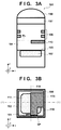
- Figs. 2A, 2B , 3A, and 3B show the arrangements of a first focus detection pixel 100 and second focus detection pixel 101 in the solid-state image sensor 10 according to the first embodiment, respectively.
- Figs. 2B and 3B are plan views of the focus detection pixels 100 and 101, and Figs. 2A and 3A are sectional views taken along lines (i) - (i) in Figs. 2B and 3B , respectively.
- the first focus detection pixel 100 is configured to detect light having passed through the first region of the pupil of an imaging optical system (not shown).
- the second focus detection pixel 101 is configured to detect light having passed through the second region of the pupil of the imaging optical system.
- the first focus detection pixel 100 includes a photoelectric converter 102 arranged in a semiconductor substrate 103, a microlens 108, and a light blocking portion 109 arranged between the semiconductor substrate 103 and the microlens 108 to cover part of the photoelectric converter 102.
- the photoelectric converter 102 is formed by, for example, doping an impurity into the semiconductor substrate 103.
- the second focus detection pixel 101 includes the photoelectric converter 102 arranged in the semiconductor substrate 103, the microlens 108, and a light blocking portion 113 arranged between the semiconductor substrate 103 and the microlens 108 to cover part of the photoelectric converter 102.
- the photoelectric converter 102 is formed by, for example, doping an impurity into the semiconductor substrate 103.
- the solid-state image sensor 10 or the focus detection pixels 100 and 101 according to the first embodiment can further include an insulating film 104 arranged between the microlens 108 and the semiconductor substrate 103, and a color filter 107 arranged between the insulating film 104 and the microlens 108.
- the light blocking portions 109 and 113 can be arranged in the insulating film 104.
- the color filter 107 may include a planarizing layer.
- a face PL which is parallel to the surface of the semiconductor substrate 103 and on which the light blocking portion 109 is arranged includes a first opening 112 and a second opening 111 in addition to the light blocking portion 109.
- the second opening 111 is preferably larger in area than the first opening 112.
- the light blocking portion 109 includes a separator SP that has a light blocking property and is arranged between the first opening 112 and the second opening 111.
- the face PL which is parallel to the surface of the semiconductor substrate 103 and on which the light blocking portion 113 is arranged includes a first opening 116 and a second opening 115 larger in area than the first opening 116, in addition to the light blocking portion 113.
- the light blocking portion 113 includes the separator SP that has a light blocking property and is arranged between the first opening 116 and the second opening 115.
- the solid-state image sensor 10 or the focus detection pixels 100 and 101 according to the first embodiment can further include wiring layers 106 between the face PL and the microlens 108 in the insulating film 104.
- Each of the focus detection pixels 100 and 101 can further include a transfer gate (transfer transistor) 105 in which a channel for transferring charges generated in the photoelectric converter 102 is formed in the semiconductor substrate 103.
- the separator SP can be arranged to cover part of the transfer gate 105.
- Boundary lines 110 between the second openings 111 and 115 and the light blocking portions 109 and 113 can be perpendicular to the direction of length of the channel formed by the transfer gate 105 (direction in which the transfer gate transfers charges).
- Contact plugs may be arranged in the first openings 112 and 116.
- the insulating film 104 is typically transparent. Although the insulating film 104 may be a monolayer film made of one type of material, the insulating film 104 can be typically a multilayer film formed by stacking a plurality of layers made of different materials. A given layer of the insulating film 104 can be made of, for example, silicon oxide (SiO 2 ). Another layer of the multilayer film constituting the insulating film 104 can be made of silicon nitride (Si 3 N 4 ) or silicon carbide (SiC).
- the wiring layer 106 can be typically multilayer wiring.
- a conductive material such as copper, aluminum, tungsten, tantalum, titanium, or polysilicon can be used for the wiring layer 106.
- the typical wiring layer 106 is opaque and has metallic luster. The same layer as the light blocking portions 109 and 113 may be used as wiring.
- the transfer gate 105 can be made of, for example, polysilicon. The transfer gate 105 can be connected to the wiring layer 106 via a contact plug.
- the color filter 107 and the microlens 108 are arranged.
- the color filter 107 is an absorption filter that transmits R (Red), G (Green), or B (Blue) light.
- the color filter 107 may be a W (White) filter that transmits beams of the R, G, and B wavelengths, or a filter that transmits IR (Infrared Ray).
- the color filter 107 may include a planarizing layer in order to improve the stability of the filter.
- the direction is expressed by the x-y-z coordinate system.
- a direction perpendicular to the surface of the semiconductor substrate 103 (direction from the semiconductor substrate 103 toward the microlens 108) is defined as the z direction.
- a face that is perpendicular to the z direction and parallel to the surface of the semiconductor substrate 103 is defined as the x-y face.
- the x and y directions are perpendicular to each other.
- the focus detection pixels 100 and 101 are paired.
- the focus detection pixel 100 includes the light blocking portion 109 on the left side (-x direction side) of the region of the focus detection pixel 100.
- the focus detection pixel 101 includes the light blocking portion 113 on the right side (+x direction) of the region of the focus detection pixel 101.
- the light blocking portion 109 can also be understood as a member that defines the first opening 112 and the second opening 111.
- the first opening 112, the separator SP, and the second opening 111 are aligned in the x direction
- the first opening 116 and the second opening 115 are also aligned in the x direction. That is, the example shown in Figs. 2A, 2B , 3A, and 3B is an example of pixels that perform focus detection on an imaging pattern having grayscale in the x direction. If focus detection pixels in which the light blocking portions 109 and 113 are rotated by 90° and arranged are used, focus detection can be performed on an imaging pattern having grayscale in the y direction.
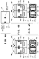
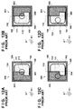
- Figs. 4A to 4C show the focus detection pixels 100 and 101 arranged in the peripheral region of the pixel region 21, and the focus detection pixels 100 and 101 arranged in the central region of the pixel region 21.
- Fig. 4B shows the section of the focus detection pixels 100 and 101 arranged in the peripheral region of the pixel region 21.
- Fig. 4C shows the section of the focus detection pixels 100 and 101 arranged in the central region of the pixel region 21.
- the microlens 108 can be shifted much more toward the center side and arranged. This can increase rays entering the photoelectric converter 102 of the focus detection pixel and improve the focus detection performance.
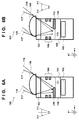
- Figs. 5A and 5B schematically show the geometrical relationship between a pupil (exit pupil) 31 of the imaging optical system and the focus detection pixels 100 and 101.
- the x direction is the pupil division direction.
- the pupil 31 includes a divided first region 33 and second region 32. It is desired that rays traveling from the first region 33 are dominant among rays entering the focus detection pixel 101, and rays traveling from the second region 32 are dominant among rays entering the focus detection pixel 100.
- Figs. 5A and 5B show a state in which light enters the focus detection pixels 100 and 101 in the peripheral region ( Fig. 4B ) within the pixel region 21.
- the angles of beams entering the focus detection pixels 100 and 101 change depending on the distances (to be referred to as pupil distances hereinafter) from the position of the pupil 31 of the imaging optical system to the focus detection pixels 100 and 101.
- Fig. 5A shows a case in which the incident angle of incident light 117 matches the shift amount of the microlens 108.
- Fig. 5B shows a case in which the pupil distance is shorter than that in Fig. 5A and the incident angle is large with respect to the shift amount of the microlens 108.
- Figs. 6A and 6B are enlarged views of the focus detection pixels 100 and 101 in Figs. 5A and 5B .
- an incident angle ⁇ from the +x direction to the -z direction is set to be ⁇ > 0, and an incident angle from the -x direction to the -z direction is set to be ⁇ ⁇ 0. Since the incident angle of the incident light 117 matches the shift amount of the microlens 108, the condensing center of the incident light 117 exists on the boundary between the second opening 111 and the light blocking portion 109 and the boundary between the second opening 115 and the light blocking portion 113.
- the focus detection accuracy is improved even in a region where the relationship between the shift of the microlens and the incident angle is improper.
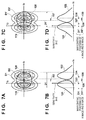
- the relationship between the incident angle distributions of the focus detection pixels 100 and 101 and the opening (aperture) of the pupil (exit pupil) of the imaging optical system will be explained. Images in the regions 32 and 33 within the pupil 31 in Figs. 5A and 5B correspond to the incident angle distributions of the focus detection pixels 100 and 101.
- the incident angle distributions of the focus detection pixels 100 and 101 are defined as an A image and a B image, respectively.
- An A image 119 in Figs. 7A and 7C is the contour drawing of an incident angle distribution determined by the focus detection pixel 100.
- a B image 120 in Figs. 7A and 7C is the contour drawing of an incident angle distribution determined by the focus detection pixel 101.
- Incident angles in the x and y directions are represented by ⁇ x and ⁇ y, respectively.
- Figs. 7B and 7D show projection data with respect to ⁇ x in Figs. 7A and 7C .
- the abscissa indicates the incident angle ⁇ x, and the ordinate indicates the sensitivity [a.u.].
- the microlens 108 is shifted in the x direction (y direction)
- the incident angle distribution is translated in the ⁇ x ( ⁇ y) direction.
- D1, D2, D1', and D2' represent angle regions where light enters.
- the angle region is determined by the opening (aperture) of the exit pupil of an imaging optical system 11 (see Fig. 21 ).
- D1 and D1' are incident angle regions when the aperture of the imaging optical system 11 is set to a full-aperture state (for example, f1.4).
- D2 and D2' are incident angle regions when the aperture is narrowed (for example, f8).
- the incident angle changes depending on the pupil distance of the imaging optical system 11.
- D1 and D2 represent a case in which the incident angle ⁇ x of the incident light 117 matches the shift amount of the microlens 108.
- D1' and D2' represent a case in which the incident angle ⁇ x is large with respect to the shift amount of the microlens 108.
- the barycentric positions of the A and B images are spaced apart from each other in the incident light angle regions D1 and D2 determined by the aperture (f-number).
- the barycentric position of a function F( ⁇ ) in an interval [a,b] is defined by: ⁇ a b ⁇ F ⁇ d ⁇ ⁇ a b ⁇ F ⁇ d ⁇
- reference numerals 123 and 124 denote barycentric positions (abscissa: ⁇ x) of the A and B images in the angle region of D1, respectively.
- Reference numerals 125 and 126 denote barycentric positions (abscissa: ⁇ x) of the A and B images in the angle region of D2, respectively.
- reference numerals 127 and 128 denote barycentric positions (abscissa: ⁇ x) of the A and B images in the angle region of D1', respectively.
- Reference numerals 129 and 130 denote barycentric positions (abscissa: ⁇ x) of the A and B images in the angle region of D2', respectively.
- the focus detection performance can be improved.
- the aperture is in a full-aperture state (f-number is small)
- the integration interval is widened, the distance between the barycenters is increased, and the focus detection performance becomes good.
- the angle regions D2 and D2 in which the aperture is narrowed (f-number is large) the integration interval is narrow, and the distance between the barycenters of the A and B images tends to be short. Since the incident angle of light changes depending on the pupil distance of the imaging optical system 11, the distance between the barycenters also changes along with this.
- the focus detection accuracy in this region is improved.
- Figs. 8A and 8B show condensed spots 131 of light condensed on the light blocking portions 109 and 113 when the incident angle ⁇ x is large with respect to the shift amount of the microlens 108.
- the condensed spots of light condensed on the light blocking portions 109 and 113 of the focus detection pixels 100 and 101 change to be condensed spots 132 in Figs. 8C and 8D .
- the condensed spot has a certain width owing to diffraction in wave optics.
- Figs. 9A to 9D show light blocking portions according to the prior art.
- Light blocking portions 202 and 203 in Figs. 9A to 9D each cover almost half the region of the photoelectric converter 102.
- the light blocking portions 109 and 113 are configured to form the openings 112 and 116.
- Figs. 9A and 9B show the condensed spots 131 formed on the light blocking portions 202 and 203 of focus detection pixels 200 and 201 when the shift amount of the microlens 108 and the incident angle ⁇ match each other.
- Figs. 9C and 9D show the condensed spots 132 formed on the light blocking portions 202 and 203 when the incident angle ⁇ is large with respect to the shift amount of the microlens 108.
- the focus detection pixels 100 and 101 respectively including the light blocking portions 109 and 113 according to the first embodiment
- the focus detection pixels 200 and 201 respectively including the light blocking portions 202 and 203 according to the prior art are compared here.
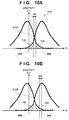
- Figs. 10A and 10B show incident angle distributions A 121 and B 122 (solid lines) of the focus detection pixels 100 and 101 according to the first embodiment, and incident angle distributions A 204 and B 205 (broken lines) of the focus detection pixels 200 and 201 according to the prior art, which are superimposed on each other.
- D2 represents the angle region D2 when the aperture is narrowed (for example, f8).
- D2 in Fig. 10A corresponds to a case in which the incident angle of light matches the shift amount of the microlens 108.
- D2' in Fig. 10B corresponds to a case in which the incident angle of light is large with respect to the shift amount of the microlens 108.
- Fig. 11A shows extractions of the A and B images in the angle region D2 of Fig. 10A .
- Reference numerals 125 and 126 denote the barycentric positions of the A and B images in the angle region D2 in the focus detection pixels 100 and 101 according to the first embodiment.
- Reference numerals 205 and 206 denote the barycentric positions of the A and B images in the focus detection pixels 200 and 201 according to the prior art.
- Fig. 11B shows extractions of the A and B images in the angle region D2' of Fig. 10B .
- Reference numerals 127 and 128 denote the barycentric positions of the A and B images in the angle region D2 in the focus detection pixels 100 and 101 according to the first embodiment.
- Reference numerals 208 and 209 denote the barycentric positions of the A and B images in the focus detection pixels 200 and 201 according to the prior art.
- the shapes of the A and B images depend on the shape of the light blocking portion.
- the light blocking portions 202 and 203 when the position of the condensed spot 132 shifts from the boundary line 110, as shown in Fig. 9C , most of light is blocked by the light blocking portion 202. If a cross point C 133 between the A image 204 and the B image 205 in Figs. 10A and 10B deviates from the boundary line 110, the sensitivity abruptly drops.
- the light blocking portions 109 and 113 according to the first embodiment when the position of the condensed spot 132 shifts from the boundary line 110, as shown in Fig. 8C , light enters the photoelectric converter 102 through the opening Q 112.
- the barycentric position depends on the center value of the angle interval and the distance between the barycenters becomes small.
- the barycentric position is spaced apart from the center value of the angle interval, and the distance between the barycenters of the A and B images can be increased.
- Figs. 12A to 12D are schematic views for examining focus detection pixels shown in Fig. 8 of Japanese Patent Laid-Open No. 2013-157883 .
- Figs. 12A to 12D show a focus detection pixel 300 including a light blocking portion 302, and a focus detection pixel 301 including a light blocking portion 303.
- the light blocking portions 302 and 303 in Figs. 12A to 12D are configured so that an opening 304 is merged with the opening 111 and an opening 305 is merged with the opening 115.
- Figs. 12A and 12B show the condensed spots 131 formed on the light blocking portions 302 and 303 of the focus detection pixels 300 and 301 when the shift amount of the microlens 108 and the incident angle ⁇ match each other.
- Figs. 12C and 12D show the condensed spots 132 formed on the light blocking portions 302 and 303 when the incident angle is large with respect to the shift amount of the microlens 108.
- Figs. 12A and 12B show the condensed spots 131 formed on the light blocking portions 302 and 303 of the
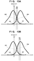
- 13A and 13B show incident angle distributions (A image and B image) 121 and 122 (solid lines) of the focus detection pixels 100 and 101 according to the first embodiment, and incident angle distributions (A image and B image) 304 and 305 (broken lines) of the focus detection pixels 300 and 301 according to the prior art, which are superimposed on each other.
- D2 represents the angle region D2 when the aperture is narrowed (for example, f8).
- D2 in Fig. 13A corresponds to a case in which the incident angle ⁇ x of light matches the shift amount of the microlens 108.
- D2' in Fig. 13B corresponds to a case in which the incident angle ⁇ x of light is large with respect to the shift amount of the microlens 108.
- Fig. 14A shows extractions of the A image 121 and B image 122 in the angle region D2 of Fig. 13A .
- Reference numerals 125 and 126 denote the barycentric positions of the A image 121 and B image 122 in the angle region D2 in the focus detection pixels 100 and 101 according to the first embodiment.
- Reference numerals 306 and 307 denote the barycentric positions of the A image 304 and B image 305 in the focus detection pixels 300 and 301 according to the prior art.
- Fig. 14B shows extractions of the A and B images in the angle region D2' of Fig. 13B .
- Reference numerals 127 and 128 denote the barycentric positions of the A image 121 and B image 122 in the angle region D2 in the focus detection pixels 100 and 101 according to the first embodiment.
- Reference numerals 308 and 309 denote the barycentric positions of the A image 304 and B image 305 in the focus detection pixels 300 and 301 according to the prior art.
- the shapes of the A and B images depend on the shape of the light blocking portion.
- the condensed spots 131 partially leak from the openings 304 and 305 and enter the photoelectric converters 102, as shown in Figs. 12A and 12B in which the incident angle and the shift amount of the microlens 108 match each other.
- the change of the sensitivity with respect to the incident angle ⁇ x becomes more gradual in comparison with the A image 121 and B image 122 of the first embodiment, and the gradient becomes smaller.
- the barycentric positions 306 and 307 of the A and B images according to the prior art come closer to each other in comparison with the barycentric positions 125 and 126 of the A and B images in the first embodiment, and the distance between the barycenters becomes short.
- the distance between the barycenters becomes larger in the first embodiment than in the prior art because of the same reason as that in Fig. 11B .
- the focus detection performance is higher in the first embodiment than in the prior art.
- the distance between the barycenters becomes larger in the first embodiment than in the prior art, and the A and B images can be clearly separated, improving the focus detection performance.
- the second opening 111 is larger in area than the first opening 112 and the second opening 115 is larger in area than the first opening 116. Further, it is preferable that the light blocking portion 109 is larger in area than the first opening 112 and smaller in area than the second opening 111, and the light blocking portion 113 is larger in area than the first opening 116 and smaller in area than the second opening 115.
- the light blocking portions 109 and 113 block almost half the condensed spots 131.
- part of light can enter the photoelectric converters 102 through the openings 112 and 116.
- the A and B images can be clearly separated, improving the focus detection performance.
- d represents the shortest distance between the first opening 112 (116) and the second opening 111 (115) (or the boundary line 110), and w represents the width (diameter) of the condensed spot 131.
- w represents the width (diameter) of the condensed spot 131.
- ⁇ represents the wavelength of incident light
- n represents the refractive index of the insulating film 104
- L represents the distance from the apex of the microlens 108 to the light blocking portion 109
- D represents the size of the focus detection pixel 100.
- the wavelength ⁇ of incident light is the maximum wavelength of the transmittance of the color filter 107.
- the wavelength ⁇ of incident light is the center wavelength of the incident light.
- the condensed spots 131 exist on the boundary lines 110, the light blocking portions 109 and 113 can block incident light, and the gradient with respect to the abscissa ⁇ x can be made steep, as in the A image 121 and the B image 122 in Figs. 11A and 14A .
- the distance between the barycenters of the A and B images can be increased, and the focus detection performance can be improved.
- d ⁇ 3w if the condensed spots 131 shift from the boundary lines 110, as shown in Figs. 8C and 8D , incident light can enter the photoelectric converters 102 through the openings 112 and 116. As shown in Fig.
- the condensed spot 131 has the distance w from the maximum peak value of the field strength to a zero point, has the distance w from the zero point to the next zero point, and has a small peak value between them.
- d ⁇ 3w a region of the condensed spot 131 where the small peak value exists enters the photoelectric converter 102 through one of the openings 111 and 115 and the opening Q 112 and 116. Accordingly, a gradient with respect to the abscissa ⁇ x can be obtained, as in the A image 121 in Figs. 11B and 14B , the distance between the barycenters of the A and B images is increased, and the focus detection performance can be improved.
- the light blocking portion 109 of the focus detection pixel 100 and the light blocking portion 113 of the focus detection pixel 101 can be configured to cover part of the transfer gates 105 in the plan view (x-y face).
- the sensitivity drops, the shape of the incident angle distribution changes, and the focus detection performance may be degraded.
- the focus detection performance By blocking light with respect to part of the transfer gate 105, degradation of the focus detection performance can be suppressed.
- the shapes of the light blocking portions 109 and 113 are not limited to the shapes as shown in Figs. 2A, 2B , 3A, and 3B and may be, for example, shapes as shown in Figs. 16A to 16H, 17A, and 17B .
- the light blocking portions 109 and 113 having the shapes shown in Figs. 17A and 17B can uniformly exert an effect in all reasons R1 to R9 within the pixel region 21 shown in Fig. 18 .
- the shapes of light blocking portions 109 and 113 are adjusted in accordance with positions in a pixel region 21.
- focus detection pixels 100 and 101 shown in Figs. 16A and 16B are arranged in regions R1, R4, and R7.
- the focus detection pixels 100 and 101 shown in Figs. 16E and 16F are arranged in regions R2, R5, and R8.
- the focus detection pixels 100 and 101 shown in Figs. 16G and 16H are arranged in regions R3, R6, and R9.
- a condensed spot is shifted to an obliquely upper left portion of the focus detection pixel on the paper surface, and it is preferable to arrange first openings 112 and 116 at upper portions on the paper surface in the region R1. As for the remaining regions, the first openings 112 and 116 are adjusted based on the same concept.
- the focus detection accuracy can be improved in all the regions R1 to R9 within the pixel region 21.
- a boundary line 110 shifts from the center of a photoelectric converter 102.
- Microlenses 108 can be shifted from the centers of focus detection pixels 100 and 101 toward the center side of the pixel region 21 and arranged in correspondence with light obliquely entering the focus detection pixels 100 and 101.
- even the boundary lines 110 between light blocking portions 109 and 113 and second openings 111 and 115 can be shifted from the centers of the focus detection pixels 100 and 101 and arranged.
- two or more types of focus detection pixels having different light blocking portions may be arranged to coexist in each region.
- focus detection pixels shown in Figs. 8A to 8D and focus detection pixels shown in Figs. 19A and 19B are arranged to coexist in a region R3. Accordingly, a more variety of imaging optical systems can be coped with in regard to the pupil distance.
- the fourth embodiment of the present invention will be described.
- the areas of first openings 112 and 116 are adjusted in accordance with the image height position in each of regions R1 to R9. A more variety of imaging optical systems can therefore be coped with in regard to the pupil distance.
- the fifth embodiment of the present invention will be described with reference to Figs. 20A and 20B .
- light blocking portions 109 and 113 are arranged at positions close to photoelectric converters 102.
- the characteristics of focus detection pixels 100 and 101 can be made closer to the characteristics of imaging pixels having neither the light blocking portion 109 nor 113.
- variations between solid-state image sensors 10 in regard to incident angle distribution characteristics as shown in Figs. 10A and 10B can be suppressed. This is because variations between the solid-state image sensors 10 owing to the influence of diffraction generated by the light blocking portion depend on variations in the distance between the light blocking portion and the photoelectric converter, and as this distance becomes shorter, variations in the distance also become smaller.
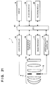
- a camera 1 according to the sixth embodiment of the present invention will be described with reference to Fig. 21 .
- the concept of the camera includes not only apparatuses mainly aiming at shooting but also apparatuses (for example, a personal computer and portable terminal) having an auxiliary shooting function.
- the camera 1 is constituted as a digital still camera and/or video camera.
- the camera 1 includes an imaging optical system 11 that forms an object image on the imaging surface of a solid-state image sensor 10.
- the imaging optical system 11 may be detachable from the body of the camera 1 or fixed to the body of the camera 1.
- a lens controller 12 can control the focus position of the imaging optical system 11.
- the imaging optical system 11 includes an aperture 13 that is controlled by an aperture controller 14. By changing the aperture diameter of the aperture 13, the intensity of light entering the solid-state image sensor 10 can be adjusted.
- the imaging surface of the solid-state image sensor 10 that converts an object image formed by the imaging optical system 11 into an electrical image signal by photoelectric conversion is arranged in the image space of the imaging optical system 11.
- the solid-state image sensor 10 can be constituted by, for example, a CMOS image sensor or a CCD image sensor.
- a CPU (controller) 15 controls various operations of the camera 1.
- the CPU 15 includes an arithmetic unit, ROM, RAM, A/D converter, D/A converter, communication interface circuit, and the like.
- the CPU 15 controls the operation of each unit of the camera 1 in accordance with a computer program stored in the ROM (not shown), and controls execution of a series of shooting operations such as AF, imaging, image processing, and recording including detection (focus detection) of the focus state of the imaging optical system 11.
- An image sensor controller 16 controls the operation of the solid-state image sensor 10, A/D-converts a pixel signal (imaging signal) output from the solid-state image sensor 10, and transmits the converted signal to the CPU 15.
- the solid-state image sensor 10 may or may not have the A/D conversion function.
- An image processor (processor) 17 performs image processes such as y conversion and color interpolation on the A/D-converted imaging signal, generating an image signal.
- a display 18 is constituted by, for example, a liquid crystal display (LCD), and displays information about the shooting mode of the camera 1, a preview image before shooting, a confirmation image after shooting, an in-focus state at the time of focus detection, and the like.
- An operation switch 19 is a switch that is operated by the user.
- a storage medium 20 is a removable recording medium, and records shot images.
- Embodiment(s) of the present invention can also be realized by a computer of a system or apparatus that reads out and executes computer executable instructions (e.g., one or more programs) recorded on a storage medium (which may also be referred to more fully as a 'non-transitory computer-readable storage medium') to perform the functions of one or more of the above-described embodiment(s) and/or that includes one or more circuits (e.g., application specific integrated circuit (ASIC)) for performing the functions of one or more of the above-described embodiment(s), and by a method performed by the computer of the system or apparatus by, for example, reading out and executing the computer executable instructions from the storage medium to perform the functions of one or more of the above-described embodiment(s) and/or controlling the one or more circuits to perform the functions of one or more of the above-described embodiment(s).
- computer executable instructions e.g., one or more programs
- a storage medium which may also be referred to more fully as
- the computer may comprise one or more processors (e.g., central processing unit (CPU), micro processing unit (MPU)) and may include a network of separate computers or separate processors to read out and execute the computer executable instructions.
- the computer executable instructions may be provided to the computer, for example, from a network or the storage medium.
- the storage medium may include, for example, one or more of a hard disk, a random-access memory (RAM), a read only memory (ROM), a storage of distributed computing systems, an optical disk (such as a compact disc (CD), digital versatile disc (DVD), or Blu-ray Disc (BD)TM), a flash memory device, a memory card, and the like.
- a solid-state image sensor includes a plurality of pixels for focus detection, each of the pixels including a photoelectric converter arranged in a semiconductor substrate, a microlens, and a light blocking portion arranged between the semiconductor substrate and the microlens to cover part of the photoelectric converter.
- a face in the pixel which is parallel to a surface of the semiconductor substrate and on which the light blocking portion is arranged, includes a first opening and a second opening in addition to the light blocking portion.
- the light blocking portion includes a separator that has a light blocking property and is arranged between the first opening and the second opening. The second opening is larger in area than the first opening, and the light blocking portion is larger in area than the first opening.
Landscapes
- Engineering & Computer Science (AREA)
- Power Engineering (AREA)
- Physics & Mathematics (AREA)
- Computer Hardware Design (AREA)
- General Physics & Mathematics (AREA)
- Condensed Matter Physics & Semiconductors (AREA)
- Electromagnetism (AREA)
- Microelectronics & Electronic Packaging (AREA)
- Multimedia (AREA)
- Signal Processing (AREA)
- Solid State Image Pick-Up Elements (AREA)
- Focusing (AREA)
- Automatic Focus Adjustment (AREA)
- Transforming Light Signals Into Electric Signals (AREA)
Applications Claiming Priority (1)
| Application Number | Priority Date | Filing Date | Title |
|---|---|---|---|
| JP2015012532A JP6518071B2 (ja) | 2015-01-26 | 2015-01-26 | 固体撮像装置およびカメラ |
Publications (1)
| Publication Number | Publication Date |
|---|---|
| EP3048645A1 true EP3048645A1 (en) | 2016-07-27 |
Family
ID=55066532
Family Applications (1)
| Application Number | Title | Priority Date | Filing Date |
|---|---|---|---|
| EP16150024.4A Withdrawn EP3048645A1 (en) | 2015-01-26 | 2016-01-04 | Solid-state image sensor and camera |
Country Status (4)
| Country | Link |
|---|---|
| US (1) | US9831278B2 (ja) |
| EP (1) | EP3048645A1 (ja) |
| JP (1) | JP6518071B2 (ja) |
| CN (1) | CN105828000B (ja) |
Cited By (1)
| Publication number | Priority date | Publication date | Assignee | Title |
|---|---|---|---|---|
| WO2023118166A1 (fr) * | 2021-12-24 | 2023-06-29 | Isorg | Capteur d'images et procede de fabrication d'un tel capteur |
Families Citing this family (21)
| Publication number | Priority date | Publication date | Assignee | Title |
|---|---|---|---|---|
| US8547428B1 (en) * | 2006-11-02 | 2013-10-01 | SeeScan, Inc. | Pipe mapping system |
| JP6408372B2 (ja) * | 2014-03-31 | 2018-10-17 | ソニーセミコンダクタソリューションズ株式会社 | 固体撮像装置及びその駆動制御方法、並びに、電子機器 |
| WO2016103430A1 (ja) * | 2014-12-25 | 2016-06-30 | キヤノン株式会社 | ラインセンサ、画像読取装置、画像形成装置 |
| WO2016194501A1 (ja) | 2015-06-03 | 2016-12-08 | ソニー株式会社 | 固体撮像素子、撮像装置、及び、固体撮像素子の製造方法 |
| JP2017069553A (ja) | 2015-09-30 | 2017-04-06 | キヤノン株式会社 | 固体撮像装置、その製造方法及びカメラ |
| JP6600246B2 (ja) | 2015-12-17 | 2019-10-30 | キヤノン株式会社 | 撮像装置及びカメラ |
| JP6732468B2 (ja) | 2016-02-16 | 2020-07-29 | キヤノン株式会社 | 光電変換装置及びその駆動方法 |
| JP6748529B2 (ja) * | 2016-09-12 | 2020-09-02 | キヤノン株式会社 | 撮像素子及び撮像装置 |
| JP6738200B2 (ja) | 2016-05-26 | 2020-08-12 | キヤノン株式会社 | 撮像装置 |
| US10319765B2 (en) | 2016-07-01 | 2019-06-11 | Canon Kabushiki Kaisha | Imaging device having an effective pixel region, an optical black region and a dummy region each with pixels including a photoelectric converter |
| JP6817835B2 (ja) | 2017-02-07 | 2021-01-20 | キヤノン株式会社 | 撮像装置及び撮像システム |
| WO2018181585A1 (ja) * | 2017-03-28 | 2018-10-04 | 株式会社ニコン | 撮像素子および撮像装置 |
| JP6653482B2 (ja) * | 2017-04-06 | 2020-02-26 | パナソニックIpマネジメント株式会社 | 撮像装置、およびそれに用いられる固体撮像装置 |
| JP2019041352A (ja) | 2017-08-29 | 2019-03-14 | キヤノン株式会社 | 撮像装置及び撮像システム |
| JP6643291B2 (ja) | 2017-09-22 | 2020-02-12 | キヤノン株式会社 | 撮像装置及びその駆動方法 |
| US10620054B2 (en) * | 2018-05-09 | 2020-04-14 | Wisconsin Alumni Research Foundation | Wavefront detector |
| WO2020045278A1 (en) | 2018-08-31 | 2020-03-05 | Canon Kabushiki Kaisha | Imaging device with motion dependent pixel binning |
| US10999540B1 (en) * | 2019-04-03 | 2021-05-04 | Apple Inc. | Camera with asymmetric field of view |
| JP7286445B2 (ja) | 2019-06-28 | 2023-06-05 | キヤノン株式会社 | 撮像装置および機器 |
| JP7538618B2 (ja) | 2020-05-01 | 2024-08-22 | キヤノン株式会社 | 光電変換装置及び光電変換システム |
| JP7171649B2 (ja) | 2020-05-15 | 2022-11-15 | キヤノン株式会社 | 撮像装置および撮像システム |
Citations (4)
| Publication number | Priority date | Publication date | Assignee | Title |
|---|---|---|---|---|
| WO2010061756A1 (en) * | 2008-11-27 | 2010-06-03 | Canon Kabushiki Kaisha | Solid-state image sensing element and image sensing apparatus |
| US20110317042A1 (en) * | 2010-06-28 | 2011-12-29 | Hisashi Goto | Image Pickup System |
| US20130182156A1 (en) * | 2012-01-13 | 2013-07-18 | Sony Corporation | Solid-state imaging device and electronic apparatus |
| JP2013157883A (ja) | 2012-01-31 | 2013-08-15 | Sony Corp | 固体撮像素子およびカメラシステム |
Family Cites Families (15)
| Publication number | Priority date | Publication date | Assignee | Title |
|---|---|---|---|---|
| JP5111157B2 (ja) | 2008-02-27 | 2012-12-26 | キヤノン株式会社 | 光電変換装置及び光電変換装置を用いた撮像システム |
| JP5398346B2 (ja) * | 2009-05-19 | 2014-01-29 | キヤノン株式会社 | 撮像装置及び信号処理装置 |
| JP5558916B2 (ja) | 2009-06-26 | 2014-07-23 | キヤノン株式会社 | 光電変換装置の製造方法 |
| JP5825817B2 (ja) * | 2011-04-01 | 2015-12-02 | キヤノン株式会社 | 固体撮像素子及び撮像装置 |
| JP5956782B2 (ja) * | 2011-05-26 | 2016-07-27 | キヤノン株式会社 | 撮像素子及び撮像装置 |
| JP6095258B2 (ja) * | 2011-05-27 | 2017-03-15 | キヤノン株式会社 | 固体撮像装置、及び固体撮像装置を用いた撮像システム |
| JP5893302B2 (ja) | 2011-09-01 | 2016-03-23 | キヤノン株式会社 | 固体撮像装置 |
| JP5956866B2 (ja) | 2011-09-01 | 2016-07-27 | キヤノン株式会社 | 固体撮像装置 |
| WO2013042518A1 (ja) * | 2011-09-22 | 2013-03-28 | 富士フイルム株式会社 | デジタルカメラ |
| US9568606B2 (en) * | 2012-03-29 | 2017-02-14 | Canon Kabushiki Kaisha | Imaging apparatus for distance detection using high and low sensitivity sensors with inverted positional relations |
| JP6308717B2 (ja) * | 2012-10-16 | 2018-04-11 | キヤノン株式会社 | 固体撮像装置、固体撮像装置の製造方法、および撮像システム |
| JP6288909B2 (ja) * | 2012-10-19 | 2018-03-07 | キヤノン株式会社 | 撮像素子及び撮像装置 |
| US9093345B2 (en) | 2012-10-26 | 2015-07-28 | Canon Kabushiki Kaisha | Solid-state imaging apparatus and imaging system |
| JP2014135355A (ja) * | 2013-01-09 | 2014-07-24 | Sony Corp | 撮像素子およびその製造方法、並びに電子機器 |
| TWI623232B (zh) * | 2013-07-05 | 2018-05-01 | Sony Corp | 固體攝像裝置及其驅動方法以及包含固體攝像裝置之電子機器 |
-
2015
- 2015-01-26 JP JP2015012532A patent/JP6518071B2/ja active Active
-
2016
- 2016-01-04 EP EP16150024.4A patent/EP3048645A1/en not_active Withdrawn
- 2016-01-15 US US14/996,774 patent/US9831278B2/en active Active
- 2016-01-21 CN CN201610040655.0A patent/CN105828000B/zh active Active
Patent Citations (4)
| Publication number | Priority date | Publication date | Assignee | Title |
|---|---|---|---|---|
| WO2010061756A1 (en) * | 2008-11-27 | 2010-06-03 | Canon Kabushiki Kaisha | Solid-state image sensing element and image sensing apparatus |
| US20110317042A1 (en) * | 2010-06-28 | 2011-12-29 | Hisashi Goto | Image Pickup System |
| US20130182156A1 (en) * | 2012-01-13 | 2013-07-18 | Sony Corporation | Solid-state imaging device and electronic apparatus |
| JP2013157883A (ja) | 2012-01-31 | 2013-08-15 | Sony Corp | 固体撮像素子およびカメラシステム |
Cited By (2)
| Publication number | Priority date | Publication date | Assignee | Title |
|---|---|---|---|---|
| WO2023118166A1 (fr) * | 2021-12-24 | 2023-06-29 | Isorg | Capteur d'images et procede de fabrication d'un tel capteur |
| FR3131440A1 (fr) * | 2021-12-24 | 2023-06-30 | Isorg | Capteur d'images et procédé de fabrication d'un tel capteur |
Also Published As
| Publication number | Publication date |
|---|---|
| JP2016138935A (ja) | 2016-08-04 |
| US20160218127A1 (en) | 2016-07-28 |
| JP6518071B2 (ja) | 2019-05-22 |
| US9831278B2 (en) | 2017-11-28 |
| CN105828000B (zh) | 2019-03-05 |
| CN105828000A (zh) | 2016-08-03 |
Similar Documents
| Publication | Publication Date | Title |
|---|---|---|
| US9831278B2 (en) | Solid-state image sensor and camera with pixel openings | |
| JP5157436B2 (ja) | 固体撮像素子および撮像装置 | |
| US10187595B2 (en) | Solid-state image sensor | |
| US8111982B2 (en) | Imaging device and electronic camera | |
| EP2762941B1 (en) | Imaging device and focus parameter value calculation method | |
| JP2005303409A (ja) | 固体撮像装置 | |
| JP2010271419A (ja) | 光学装置及び焦点検出方法 | |
| US20160073016A1 (en) | Sensor with focus detection units | |
| US10063765B2 (en) | Image pickup apparatus and camera | |
| WO2012073727A1 (ja) | 撮像装置及びその合焦位置検出方法 | |
| JP2002170944A (ja) | 固体撮像装置 | |
| US10276612B2 (en) | Photoelectric conversion apparatus and image pickup system | |
| EP3522223A1 (en) | Imaging element and focus adjustment device | |
| JP5800573B2 (ja) | 撮像装置、カメラシステムおよび焦点検出方法 | |
| US10665734B2 (en) | Image sensor and image capturing apparatus | |
| US20190258026A1 (en) | Image sensor and focus adjustment device | |
| JP5060216B2 (ja) | 撮像装置 | |
| WO2018062559A1 (ja) | 撮像素子、焦点検出装置、及び、電子カメラ | |
| JP2009065095A (ja) | 固体撮像素子 | |
| WO2018061941A1 (ja) | 撮像素子および撮像装置 | |
| US20190267422A1 (en) | Image sensor and focus adjustment device | |
| JP5537618B2 (ja) | 撮像装置 | |
| WO2018061940A1 (ja) | 撮像素子および焦点調節装置 | |
| US20220028914A1 (en) | Image sensor and image capturing apparatus | |
| JP5836629B2 (ja) | 撮像素子、それを具備する撮像装置及びカメラシステム |
Legal Events
| Date | Code | Title | Description |
|---|---|---|---|
| PUAI | Public reference made under article 153(3) epc to a published international application that has entered the european phase |
Free format text: ORIGINAL CODE: 0009012 |
|
| AK | Designated contracting states |
Kind code of ref document: A1 Designated state(s): AL AT BE BG CH CY CZ DE DK EE ES FI FR GB GR HR HU IE IS IT LI LT LU LV MC MK MT NL NO PL PT RO RS SE SI SK SM TR |
|
| AX | Request for extension of the european patent |
Extension state: BA ME |
|
| 17P | Request for examination filed |
Effective date: 20170127 |
|
| RBV | Designated contracting states (corrected) |
Designated state(s): AL AT BE BG CH CY CZ DE DK EE ES FI FR GB GR HR HU IE IS IT LI LT LU LV MC MK MT NL NO PL PT RO RS SE SI SK SM TR |
|
| STAA | Information on the status of an ep patent application or granted ep patent |
Free format text: STATUS: THE APPLICATION HAS BEEN WITHDRAWN |
|
| 18W | Application withdrawn |
Effective date: 20190426 |