EP3043396A1 - Cellule mémoire non volatile résistive et son procédé de fabrication - Google Patents
Cellule mémoire non volatile résistive et son procédé de fabrication Download PDFInfo
- Publication number
- EP3043396A1 EP3043396A1 EP16150341.2A EP16150341A EP3043396A1 EP 3043396 A1 EP3043396 A1 EP 3043396A1 EP 16150341 A EP16150341 A EP 16150341A EP 3043396 A1 EP3043396 A1 EP 3043396A1
- Authority
- EP
- European Patent Office
- Prior art keywords
- metal
- layer
- stoichiometric
- metal oxide
- memory cell
- Prior art date
- Legal status (The legal status is an assumption and is not a legal conclusion. Google has not performed a legal analysis and makes no representation as to the accuracy of the status listed.)
- Granted
Links
Images

Classifications
-
- H—ELECTRICITY
- H10—SEMICONDUCTOR DEVICES; ELECTRIC SOLID-STATE DEVICES NOT OTHERWISE PROVIDED FOR
- H10N—ELECTRIC SOLID-STATE DEVICES NOT OTHERWISE PROVIDED FOR
- H10N70/00—Solid-state devices having no potential barriers, and specially adapted for rectifying, amplifying, oscillating or switching
- H10N70/20—Multistable switching devices, e.g. memristors
- H10N70/24—Multistable switching devices, e.g. memristors based on migration or redistribution of ionic species, e.g. anions, vacancies
-
- H—ELECTRICITY
- H10—SEMICONDUCTOR DEVICES; ELECTRIC SOLID-STATE DEVICES NOT OTHERWISE PROVIDED FOR
- H10B—ELECTRONIC MEMORY DEVICES
- H10B63/00—Resistance change memory devices, e.g. resistive RAM [ReRAM] devices
-
- H—ELECTRICITY
- H10—SEMICONDUCTOR DEVICES; ELECTRIC SOLID-STATE DEVICES NOT OTHERWISE PROVIDED FOR
- H10N—ELECTRIC SOLID-STATE DEVICES NOT OTHERWISE PROVIDED FOR
- H10N70/00—Solid-state devices having no potential barriers, and specially adapted for rectifying, amplifying, oscillating or switching
- H10N70/011—Manufacture or treatment of multistable switching devices
- H10N70/021—Formation of switching materials, e.g. deposition of layers
-
- H—ELECTRICITY
- H10—SEMICONDUCTOR DEVICES; ELECTRIC SOLID-STATE DEVICES NOT OTHERWISE PROVIDED FOR
- H10N—ELECTRIC SOLID-STATE DEVICES NOT OTHERWISE PROVIDED FOR
- H10N70/00—Solid-state devices having no potential barriers, and specially adapted for rectifying, amplifying, oscillating or switching
- H10N70/011—Manufacture or treatment of multistable switching devices
- H10N70/021—Formation of switching materials, e.g. deposition of layers
- H10N70/023—Formation of switching materials, e.g. deposition of layers by chemical vapor deposition, e.g. MOCVD, ALD
-
- H—ELECTRICITY
- H10—SEMICONDUCTOR DEVICES; ELECTRIC SOLID-STATE DEVICES NOT OTHERWISE PROVIDED FOR
- H10N—ELECTRIC SOLID-STATE DEVICES NOT OTHERWISE PROVIDED FOR
- H10N70/00—Solid-state devices having no potential barriers, and specially adapted for rectifying, amplifying, oscillating or switching
- H10N70/011—Manufacture or treatment of multistable switching devices
- H10N70/041—Modification of switching materials after formation, e.g. doping
-
- H—ELECTRICITY
- H10—SEMICONDUCTOR DEVICES; ELECTRIC SOLID-STATE DEVICES NOT OTHERWISE PROVIDED FOR
- H10N—ELECTRIC SOLID-STATE DEVICES NOT OTHERWISE PROVIDED FOR
- H10N70/00—Solid-state devices having no potential barriers, and specially adapted for rectifying, amplifying, oscillating or switching
- H10N70/011—Manufacture or treatment of multistable switching devices
- H10N70/041—Modification of switching materials after formation, e.g. doping
- H10N70/043—Modification of switching materials after formation, e.g. doping by implantation
-
- H—ELECTRICITY
- H10—SEMICONDUCTOR DEVICES; ELECTRIC SOLID-STATE DEVICES NOT OTHERWISE PROVIDED FOR
- H10N—ELECTRIC SOLID-STATE DEVICES NOT OTHERWISE PROVIDED FOR
- H10N70/00—Solid-state devices having no potential barriers, and specially adapted for rectifying, amplifying, oscillating or switching
- H10N70/20—Multistable switching devices, e.g. memristors
-
- H—ELECTRICITY
- H10—SEMICONDUCTOR DEVICES; ELECTRIC SOLID-STATE DEVICES NOT OTHERWISE PROVIDED FOR
- H10N—ELECTRIC SOLID-STATE DEVICES NOT OTHERWISE PROVIDED FOR
- H10N70/00—Solid-state devices having no potential barriers, and specially adapted for rectifying, amplifying, oscillating or switching
- H10N70/801—Constructional details of multistable switching devices
- H10N70/821—Device geometry
-
- H—ELECTRICITY
- H10—SEMICONDUCTOR DEVICES; ELECTRIC SOLID-STATE DEVICES NOT OTHERWISE PROVIDED FOR
- H10N—ELECTRIC SOLID-STATE DEVICES NOT OTHERWISE PROVIDED FOR
- H10N70/00—Solid-state devices having no potential barriers, and specially adapted for rectifying, amplifying, oscillating or switching
- H10N70/801—Constructional details of multistable switching devices
- H10N70/821—Device geometry
- H10N70/826—Device geometry adapted for essentially vertical current flow, e.g. sandwich or pillar type devices
-
- H—ELECTRICITY
- H10—SEMICONDUCTOR DEVICES; ELECTRIC SOLID-STATE DEVICES NOT OTHERWISE PROVIDED FOR
- H10N—ELECTRIC SOLID-STATE DEVICES NOT OTHERWISE PROVIDED FOR
- H10N70/00—Solid-state devices having no potential barriers, and specially adapted for rectifying, amplifying, oscillating or switching
- H10N70/801—Constructional details of multistable switching devices
- H10N70/841—Electrodes
-
- H—ELECTRICITY
- H10—SEMICONDUCTOR DEVICES; ELECTRIC SOLID-STATE DEVICES NOT OTHERWISE PROVIDED FOR
- H10N—ELECTRIC SOLID-STATE DEVICES NOT OTHERWISE PROVIDED FOR
- H10N70/00—Solid-state devices having no potential barriers, and specially adapted for rectifying, amplifying, oscillating or switching
- H10N70/801—Constructional details of multistable switching devices
- H10N70/881—Switching materials
- H10N70/883—Oxides or nitrides
- H10N70/8833—Binary metal oxides, e.g. TaOx
Definitions
- the present invention generally relates to non-volatile memories with resistive elements. It more particularly describes a resistive non-volatile memory cell and its manufacturing method.
- the invention will find its application possibly in all the applications already covered by the existing non-volatile memories; in particular, memories of Flash type. Because of their access time and their ease of writing, non-volatile memories with resistive elements can also replace the static traditional memory or SRAM, the static random access memory.
- the invention will also find its application for the production of memory structures of the neuromorphic type or for CBRAM memories for the acronym "Conductive Bridge Ramdom Access Memory” or in nanoelectronic devices based on the principle of transitions Metal / Insulator also called “Mott insulator”, such as for example Mott selectors, Mott transistors, devices including photo-induced Mott transitions.
- Mott insulator such as for example Mott selectors, Mott transistors, devices including photo-induced Mott transitions.
- the resistive element memories use a material that can switch reversibly between at least two stable states having different electrical resistances.
- Resistive memories are generally referred to as RRAM, the acronym for “resistive random access memory”, that is, “resistive memory with random access”.
- OxRAM metal oxides
- LRS low resistance state
- HRS high resistance state
- non-volatile resistive memory structures have a reservoir of oxygen vacancies located in contact with the electrodes. This requires the use of electrodes insensitive to oxygen movements / gaps including electrodes made of noble materials. However, the use of noble electrodes strongly limits the use of such a stack in an integration with the standard of microelectronics where only a certain number of metals, not including noble metals, have shown their immunities -vis the operation of a transistor.
- non-noble electrode often leads to an increase in the variability from one device to another as well as to a low reliability of the memory cell in terms of cycling and retention time.
- the present invention aims to meet at least some of these issues.
- the present invention proposes for this purpose a resistive nonvolatile memory cell comprising a metal-insulator-metal type stack with a lower electrode and an upper electrode and in which the insulator is a multilayer comprising a stoichiometric metal oxide layer and a a stoichiometric metal oxide layer forming an oxygen vacancy reservoir layer and wherein the metal layer forming the upper electrode comprises a stoichiometric metal oxide layer below said metal layer.
- This arrangement makes it possible to place the oxygen vacancy reservoir layer between two stoichiometric metal oxide layers removing the contact between said gap reservoir layer and the electrodes. In this way the amount of oxygen vacancies in the reservoir is stable over time and cycling of the memory.
- the selection of materials for the electrodes extend outside the noble metals which allows integration of the memory cell according to the invention to the standard of microelectronics in a transistor.
- a contact between a reservoir of oxygen vacancies and a non-noble electrode can induce a variation of the amount of oxygen in the reservoir of vacancies.
- oxygen as a function of time or during the cycling of the memory cell may result in an increase in variability from one device to another.
- the invention thus makes it possible to respond to this problem. It also makes it possible to improve the reliability of the memory cells in terms of cycling and retention as a function of time.
- the electrodes are non-noble metals.
- the metals M1 of the lower electrode, M2 of the multilayer insulator and M3 of the stoichiometric metal oxide layer are chosen so that the metal M3 reduces the stoichiometric metal oxide 12 of the insulator but not a stoichiometric metal oxide I1 potentially present on the surface of the metal layer forming the lower electrode.
- the free formation enthalpy DG3 of the stoichiometric metal oxide 13 by oxidation of a metal M3 is greater in absolute value than the free formation enthalpy DG2 of the stoichiometric metal oxide 12 by oxidation of a metal M2 .
- the free formation enthalpy DG1 of the stoichiometric metal oxide I1 by oxidation of a metal M1 is greater than or equal in absolute value to the free formation enthalpy DG3 of the stoichiometric metal oxide 13 by oxidation of a M3 metal.
- the invention relates to a method of manufacturing a memory cell according to any one of the preceding claims comprising the following successive steps of deposition of a metal layer M1 to form the lower electrode, of deposit of a metal oxide layer 12, depositing a metal layer M3, reacting the metal layer M3 with the stoichiometric metal oxide 12 forming a stoichiometric oxide I2p and a metal oxide 13, depositing a metal layer M4.
- the invention relates to a microelectronic device characterized in that it comprises a memory cell as described above.
- the device comprises a cavity in which the memory cell is at least partially arranged.
- the memory cell is entirely comprised in the cavity.
- This provision makes it possible by confinement effect to overcome the impact of the exogenous oxygen provided by the successive steps during the manufacture of such a device and in particular during the deposition of interconnection oxide. This makes it possible to consider locating the filament in a well-defined and preferably centered region of the stack, which leads to a reduction in the potential for forming the filament Vf by constricting the current lines passing through the stack. This integration also makes it possible to reduce the variability of the on-state of the device.
- metals M2 and M3 respectively to form the insulator 12 and I2p and to form the stoichiometric metal oxide layer 13 are chosen so that the free formation enthalpy DG3 of the stoichiometric metal oxide 13 by oxidation of the metal M3 is greater in absolute value than the free formation enthalpy DG2 of the stoichiometric metal oxide 12 by oxidation of the metal M2.
- the lower electrode comprises above the metal layer M1, a metal oxide layer I1 of M1.
- the metals M1 and M3 are chosen so that the free formation enthalpy DG1 of the oxide I1 by oxidation of a metal M1 is greater than or equal in absolute value to the free formation enthalpy DG3 of the oxide 13 by oxidation of an M3 metal.
- the metal M1 is chosen so that the free formation enthalpy DG1 of the oxide I1 by oxidation of a metal M1 is greater than or equal in absolute value to the free formation enthalpy DG of the reaction 2Cu + O2 -> 2CuO.
- the metals M1 and M4 are chosen from a non-noble metal other than Pd, Ag, Ir, Pt, Au, or a pure metal or a binary or ternary metal alloy, or an alloy based on nitride or carbide or silicide or conductive metal oxide.
- the metals M1 and M4 are chosen from TiN, TaN, TiAlN, TaAlN.
- the lower electrode and the upper electrode are symmetrical in the stack.
- the stoichiometric metal oxide layer I1 of M1 is selected from TiO2 or TiON or Al2O3.
- the stoichiometric oxide layer 12 is formed from a metal M2 chosen from columns III, IV, V, of the periodic table, or Al or Si, or lanthanides.
- the stoichiometric oxide layer 12 is chosen from HfO2, ZrO2, TiO2, Al2O3, Ta2O5, Nb2O5, V2O5, La2O4, Gd2O3, Lu2O3, HfSiO, HfZrO, STO.
- the stoichiometric oxide layer 12 of a metal M2 has a thickness of 1 to 50 nm.
- the metal oxide layer 13 is formed from a metal M3 selected from a pure metal or a binary or ternary metal alloy.
- the metal M3 is chosen from Si, Ti, Zr, Hf, Al, Ta, Nb, V, and the alloys in a mixture of these elements, for example TiAl, TaAl.
- the stack comprises from bottom to top: TiN / TiO2 / Ta2O5 / TaOx / TiO2 / TiN, or TiN / TiO2 / Ta2O5 / TaOx / Nb2O5 / TiN, or TiN / TiO2 / V2O5 / VOx / Nb2O5 / TiN, or TiN / TiO2 / V2O5 / VOx / Nb2O5 / TiN, or TiN / TiO2 / V2O5 / VO / Ta2O5 / TiN
- the deposition of the metal layer M3 is carried out by flash vapor deposition.
- the deposition of the metal layer M3 is not a compliant deposit. This makes it possible to simplify the realization.
- the metal layer M3 is deposited on a thickness of 0.1 to 2 nm.
- the stoichiometric metal oxide layer 12 is deposited chemically.
- the stoichiometric metal oxide layer 12 is treated with plasma or by plasma nitriding.
- the stoichiometric metal oxide layer 12 is implanted with aluminum.
- Another object of the invention is a microelectronic device characterized in that it comprises a memory cell as described above.
- the device comprises a cavity in which the memory cell is at least partially arranged.
- the cavity is formed of an electrically insulating material, such as an oxide.
- the lower electrode of the memory cell is arranged below and outside the cavity.
- the lower electrode of the memory cell is arranged in the cavity.
- the device comprises a plurality of interconnection level and a plurality of connection plug between the levels, each plug comprising a cavity in which at least a memory cell as described above is at least partially arranged.
- the method comprises the conformal deposition of a metal layer M1 in the cavity to form the lower electrode before the deposition of the stoichiometric metal oxide layer 12.
- the method comprises depositing a metal layer M5 to plug the cavity.
- the deposition of the metal layer M3 is carried out by flash vapor deposition.
- the metal layer M3 is deposited on a thickness of 0.1 to 2 nm.
- the stoichiometric metal oxide layer 12 is deposited chemically.
- the stoichiometric metal oxide layer 12 is treated with plasma or by plasma nitriding.
- the stoichiometric metal oxide layer 12 is implanted with aluminum.
- the term “over”, “overcomes” or “underlying” or their equivalents do not necessarily mean “in contact with”.
- the deposition of a first layer on a second layer does not necessarily mean that the two layers are in direct contact with one another but that means that the first layer at least partially covers the second layer by being either directly in contact with it or separated from it by another layer or another element.
- thin layer a layer whose thickness varies from a few atomic layers to a few microns.
- microelectronic device any type of device made with microelectronics means. These devices include, in addition, devices for purely electronic purposes, micromechanical or electromechanical devices (MEMS, NEMS, etc.) as well as optical or optoelectronic devices (MOEMS, etc.).
- MEMS micromechanical or electromechanical devices
- MOEMS optical or optoelectronic devices
- the memory cell according to the invention is a stack of layers of the Metal-Insulator-Metal (MIM) type, more specifically of the Metal-Oxide-Metal (MOM) type.
- MIM Metal-Insulator-Metal
- MOM Metal-Oxide-Metal
- the memory cell is a nonvolatile memory with resistance change.
- Resistive Random Access Memory (RRAM) relies on the change of resistance of an active material, more precisely in the sub-category of OxRRAM (Oxide RRAM) the active material is an oxide forming an insulator 2.
- the two layers on both sides of the insulator 2 are electrodes 1, 3.
- the stack according to a preferred embodiment of the invention is represented in FIG. figure 1 .
- the stack comprises from bottom to top: a metal layer M1, optionally a metal oxide layer 11, a stoichiometric metal oxide layer 12, a stoichiometric metal oxide layer I2p, a stoichiometric metal oxide layer 13 and a metal layer M4.
- a lower electrode 1 also called “bottom electrode” in English comprises the metal layer M1 and potentially over a metal oxide layer I1.
- the metal layer M1 is formed by a non-noble metal.
- Noble means a metal that does not spontaneously oxidize in the air.
- the noble metals are silver (Ag), Iridium (Ir), Platinum (Pt), gold (Au) and palladium (Pd).
- the metal layer M1 may be a pure metal or a binary or ternary metal alloy such as, for example, TiAl, TaAl, TiAlN, TaAlN or else an alloy based on nitride, or carbide, or silicide, or on conductive metal oxide, preferentially TiN, TaN.
- the metal oxide I1 is an oxide that can be formed during the manufacturing process of the memory cell.
- the metal of the metal layer M1 can be oxidized by the air in contact, or by a stoichiometric metal oxide 12 described hereinafter.
- the metal layer M1 can also be intentionally oxidized to form the metal oxide I1.
- the metal oxide I1 is deposited, for example to form a selector or diode non-linear resistance.
- the metal oxide I1 is TiO2 or TiON.
- An insulator 2 advantageously comprises at least two layers of materials also called a multilayer, the insulator 2 is preferably a bilayer.
- the bi-layer comprises a stoichiometric metal oxide layer 12 and a stoichiometric metal oxide layer I2p.
- stoichiometric is understood as the proportion of elements in a crude formula.
- a stoichiometric layer according to the invention has a proportion of oxygen less than the stoichiometric proportion of the compound.
- the stoichiometric metal oxide 12 constitutes the active layer having a resistive variation as a function of an applied voltage.
- the stoichiometric metal oxide I2p constitutes a reservoir layer of oxygen vacancies. This layer is an oxide having a lesser amount of oxygen than the stoichiometric oxide. This oxygen deficiency is defined as oxygen deficiency. The more oxygen deficient the material, the more conductive it is. This oxygen vacancy reserve layer I2p makes it possible to facilitate the resistivity variations of the oxide layer 12. In fact, the two layers 12 and 12 interact during the SET and RESET phases so as to allow the formation of the filaments. conductors between the two electrodes 1 and 3.
- the stoichiometric metal oxide layer 12 is advantageously a thin layer.
- the stoichiometric metal oxide 12 is a metal stoichiometric oxide. This oxide 12 is chosen from columns III, IV, V, of the Periodic Table, or Aluminum (Al) or Silicon (Si), or a lanthanide, for example HfO 2, ZrO 2, TiO 2, Al 2 O 3, Ta 2 O 5, Nb 2 O 5, La2O4, Gd2O3, Lu2O3, or ternary compounds HfSiO, HfZrO, STO.
- the stoichiometric metal oxide 12 is preferably Ta2O5.
- the stoichiometric metal oxide layer 12 is deposited chemically.
- its thickness is between 1 nm and 50 nm.
- the stoichiometric metal oxide 12 is plasma treated. This type of treatment makes it possible to modulate the final thickness L and / or the oxygen depletion profile of the stoichiometric metal oxide layer I2p.
- treatments of the plasma nitriding type radio-frequency plasma or microwave N2 with nitrogen or nitriding in a reducing atmosphere typically in a hydrogenated atmosphere N2 + H2.
- the stoichiometric metal oxide layer 12 is processed by implantation. The implantation can be made directly in the layer 12 or through the stoichiometric metal oxide layer 13 and the stoichiometric metal oxide layer 12p. This implantation treatment makes it possible to promote the formation of conductive filaments between the lower electrode 1 and the upper electrode 3 of the stack of the memory cell. For example, an aluminum implantation can be performed.
- the metal oxide I2p is a sub stoichiometric oxide. This oxide I2p is not voluntarily deposited but comes from a reaction with a metal M3 deposited on top of the stoichiometric metal oxide 12.
- the metal M3 is preferably a pure metal or a binary or ternary metal alloy, for example TiAl, TaAl, preferably pure titanium (Ti).
- the metal M3 is deposited by flash vapor deposition (PVD flash).
- flash corresponds to the control over a very short time, advantageously of the order of one second, the deposit of a film of some Angstrom.
- the deposited metal layer M3 is of a thickness of 0.1 nm to 2 nm. The control of this time makes it possible very advantageously to deposit very precisely the quantity of metal M3 desired so as to be able to modulate the depth of oxygen depletion in the stoichiometric metal oxide layer 12 and the final thickness L of the metal oxide layer. under stoichiometric I2p.
- the flash time will make it possible to define the final thickness of the stoichiometric metal oxide 13.
- the type of metal deposition M3 influences the overall resistivity of the memory cell.
- the flash deposit makes it possible to form localized islands, also called dots, nanodots or nanocrystals, making it possible to locally reduce the stoichiometric metal oxide layer 12, and thus make it possible to locate the conductive filaments 4 in the layer of stoichiometric metal oxide 12.
- the deposited metal M3 is no longer present as a metal in the finalized memory cell.
- the metal M3 is configured to react with the stoichiometric metal oxide layer 12. This reaction leads to a partial reduction of the stoichiometric metal oxide 12 to a stoichiometric metal oxide I2p and to the oxidation of the metal M3 to a layer of metal.
- Stoichiometric metal oxide 13 As a preferred example, the metal M3 is pure titanium which reacts with the stoichiometric metal oxide I2, Ta2O5, to form the stoichiometric metal oxide. 13, TiO 2, and the stoichiometric metal oxide I 2p, TaO 2. This reaction can according to one possibility be activated thermally.
- the reduction of the oxide 12 by the metal M3 is possible if the free formation enthalpy (DG3) of the reaction M3 + O2-> I3 is greater in absolute value than the free formation enthalpy (DG2) of the reaction M2 + O2-> I2.
- An Elligham chart can typically be used to predict the direction of the reactions.
- the amount of metal M3 deposited is very small compared to the thickness of 12 so as not to consume the entire stoichiometric metal oxide 12 without being able to obtain the oxygen depletion profile referred to in the metal oxide under stoichiometric 12p .
- the metal M3 reduces the stoichiometric metal oxide layer 12, but not an oxide layer I1 possibly present on the surface of the metal layer M1. Therefore, it is advantageous for the free formation enthalpy (DG1) of the reaction M1 + O2 -> I1 to be greater than or equal in absolute value to the free enthalpy (DG3) forming the reaction M3 + O2-> I3.
- the free formation enthalpy DG1 of the oxide I1 by oxidation of a metal M1 is greater than or equal in absolute value to the free formation enthalpy DG of the reaction 2Cu + O2-> 2CuO .
- An upper electrode 3 also called "top electrode” in English comprises the metal layer M4 and a stoichiometric metal oxide layer 13.
- the metal oxide layer 13 forms an insulating layer for isolating the metal layer M4 partially forming the upper electrode 3 of the stoichiometric metal oxide layer I2p constituting the oxygen vacancy reservoir layer. The presence of this insulating layer 13 eliminates noble electrodes not likely to be oxidized.
- the metal layer M4 is formed by a non-noble metal.
- Noble means a metal that does not spontaneously oxidize in the air.
- the noble metals are silver (Ag), Iridium (Ir), Platinum (Pt), gold (Au) and palladium (Pd).
- the metal layer M4 may be a pure metal or a binary or ternary metal alloy such as for example TiN, TaN, TiAlN, TaAlN or else an alloy based on nitride, or carbide, or silicide, or oxide conductive metal, preferably TiN, TaN.
- the lower electrode 1 and the upper electrode 3 are symmetrical. Symmetrical means that the two electrodes 1 and 3 are of the same thickness, the same properties, the same materials.
- the stack of the memory cell consists of TiN / TiO2 / Ta2O5 / TaOx / TiO2 / TiN, or TiN / TiO2 / Ta2O5 / TaOx / Nb2O5 / TiN, or TiN / TiO2 / V2O5 / VOx / Nb2O5 / TiN, or TiN / TiO2 / V2O5 / VOx / Ta2O5 / TiN
- an oxygen profile as illustrated in figure 2 is particularly sought after. It can be seen in this figure that the stoichiometric metal oxide layer I2p exhibits oxygen depletion relative to the other stoichiometric metal oxide layers 11, 12 and 13 of the stack.
- L denotes I2P the thickness of the stoichiometric metal oxide 12 and small I I2P the thickness of the depletion profile.
- the depletion profile is characterized by I2P ⁇ L I2P .
- the present invention also relates to a method of manufacturing a memory cell as described above.
- Such a method comprises a series of successive steps including the deposition of the metal layer M1, then the deposition of the stoichiometric metal oxide 12 and then the deposition of a metal layer M3 and then the formation of the stoichiometric metal oxide layer 13 and the stoichiometric metal layer 12p by reaction between the metal M3 and the stoichiometric oxide 12, then the deposition of a metal layer M4.
- the reaction between the metal layer M3 and the stoichiometric metal oxide 12 is advantageously controlled by the choice of metals M1, M2 and M3.
- the free formation enthalpy (DG3) of the reaction M3 + O2-> I3 is greater in absolute value than the free formation enthalpy (DG2) of the reaction M2 + O2-> I2.
- DG1 free formation enthalpy of the reaction M1 + O2 -> I1
- DG3 free formation enthalpy
- the metal layer M3 reduces the stoichiometric metal oxide layer 12, but not a stoichiometric oxide layer I1 possibly present on the surface of the metal layer M1.
- a memory cell according to the invention can be integrated into various microelectronic devices ranging from portable data storage devices to neuromorphic memory structures.
- the integration of the active films of a memory cell according to the invention as described above, is currently done in the Back-End lines of microelectronic devices using memory cells, at a metal level Mi, the index i being an integer that represents the number of interconnect levels in a device.
- These films are deposited in planar on the surface of a plug. Then, an etching step makes it possible to define the final size of the memory cell. Finally, a new plug is created on the upper stage (Mi + 1) and connects the upper electrode of the memory cell.
- the formation of a plug requires the deposition of a low temperature oxide, the etching of a hole aligned on the upper electrode, then the deposition in this hole of a contact metal, typically TiN / W or Ta / TaN / Cu.
- the deposition of the low temperature oxide brings exogenous oxygen into contact with the memory cell and causes a deterioration of the properties of the cell.
- This type of oxygen capping with SiN is widely used for CMOS transistors.
- this SiN film also undergoes a thickness reduction in order to follow the overall geometry of the devices. For example, in the lines of the Mi levels, the thickness of the level represents approximately 2 to 3 times the width of the plug.
- the minimum thickness of the SiN film proposed in this document is 20 nm.
- a film of 20 nm represents approximately 1/3 of the height of the level Mi.
- the SiO2 plasma deposition process impacts the underlying films. Indeed, the treatment plasma used in situ during the deposition of the inter-plug insulator is physically penetrating and type O * species can pass through the SiN protective film.
- the memory cell as described above can be arranged at least partially in a cavity 6 also called "via".
- the invention will also find application for microelectronic and nanoelectronic devices comprising a plurality of interconnection levels and a plurality of connection plugs between the levels.
- Each plug comprises a cavity 6.
- the cavity 6 has a width 8 of opening less than 180 nm, preferably equal to or less than 65 nm.
- the cavity 6 is formed in chemically deposited SiO 2 oxide to form an interconnection plug leading to a level 7 connection line. lower Mi-1. More generally, the cavity 6 is formed of an electrically insulating material.
- the stack of the memory cell is partially arranged in the cavity 6.
- the connection line 7 of the lower level Mi-1 forms the metal layer M1 and optionally its stoichiometric metal oxide layer I1. This is possible when the connection line 7 is in Al, Ta, TaN or TiN.
- the stoichiometric metal oxide layer I1 is then Al2O3, TiO2, TiON, Ta2O5, TaON.
- the metal layer M1 of the lower electrode 1 and optionally the stoichiometric metal oxide layer I1 are arranged outside and under the cavity. Under which is meant that the metal layer M1 is present before the formation of the cavity, and outside is understood to mean that the metal layer M1 is of greater length than the width of the cavity 6.
- the cavity 6 comprises from bottom to top, the insulator 2 comprising the stoichiometric metal oxide layer 12 and the stoichiometric metal oxide layer I2p forming said oxygen vacancy reservoir layer and then the stoichiometric metal oxide layer. 13 and the metal layer M4.
- the stoichiometric metal oxide layer I1 is advantageously present for maintaining the sub-stoichiometric metal oxide layer I2p in contact with stoichiometric metal oxide layers 11, 12 and 13.
- the stack of the memory cell is entirely arranged in the cavity 6.
- the connection line 7 of the lower level Mi-1 does not form the metal layer M1.
- the metal layer M1 of the lower electrode 1 and possibly the stoichiometric metal oxide layer I1 are arranged in In this embodiment, it is noted that the insulator 2 formed at least by the stoichiometric metal oxide layer 12 conforms ensures the electrical insulation between the metal layers M1 and M4.
- the metal layer M1 then acts as a barrier intended to limit the diffusion of the material of the connection line 7 in the memory cell.
- the method of manufacturing a memory cell comprises the steps described below.
- the deposition of the stoichiometric metal oxide layer 12 is carried out by chemical vapor deposition (CVD acronym).
- CVD acronym chemical vapor deposition
- the term "compliant deposition” is understood to mean that the deposition is carried out in the bottom and on the walls of the cavity 6.
- the deposition of a layer of metal M3 at the bottom of the cavity preferably deposited by physical flash vapor deposition (PVD acronym), by example flash Ti, Al, Zr, Hf, Si, Ta, Nb, V.
- the method comprises a step of capping the cavity 6.
- At least one metal layer M4 is deposited in the cavity 6.
- the metal layer M4 is advantageously impermeable to oxygen such as for example Co, Ni, Cu.
- the deposits of the metal layers M1 and M4 are advantageously made as for the stack illustrated in FIG. figure 1 .
- the reaction of the metal layer M3 with the stoichiometric metal oxide 12 results in the formation of the sub-stoichiometric oxide I2p located around, more precisely in the immediate vicinity, of the stoichiometric metal oxide layer 13.
- This reaction can be assisted by annealing typically aligned with back end annealing at about 400 ° C.
- the exogenous oxygen-sensitive layer I2p is found buried in the cavity bottom 6, protected from oxidation by insulating layers: the residual stoichiometric metal oxide 12 (that has not reacted) and the stoichiometric metal oxide 13 and the metal layer M4.
- the method comprises a step of de-contact plugs of the same level comprising a chemical mechanical polishing (acronym CMP).
- acronym CMP chemical mechanical polishing
- the stoichiometric metal oxide layer 12 has a width L of between 2 and 20 nm. This width L is understood as the dimension separating the walls of the cavity 6 from the stoichiometric metal oxide layer 13.
- the stoichiometric metal oxide layer 13 has a width I of between 10 and 40 nm, preferably 25 nm.
- width L of the stoichiometric metal oxide layer 12 is 10 nm and width I of the stoichiometric metal oxide layer 13 is 25 nm.
- This stacking arrangement makes it possible to confine / locate the filament of gaps under the stoichiometric metal oxide layer 13 of width I.
- the current lines are located in a limited area increasing the temperature rise. local. This constriction of the current lines makes it possible to reduce the formation potential of the filament Vf.
- the formation potential Vf is advantageously less than 3V and preferably of the order of 2V thus allowing integration of the memory cell according to the invention into CMOS devices.
- the invention also has the advantage of reducing the variability of the on state, Ron, of the memory cell.
- the capping of the cavity can be achieved by stacking several layers. As illustrated in Figures 6 to 9 two metal layers M4 and M5 are deposited in the cavity 6 to close it.
- the metal layer M4 may be TiN or TaN.
- the metal layer M5 is an oxygen impermeable metal such as cobalt, nickel or copper.
- the manufacturing method comprises a step of disconnecting the metal layers M1 and M5, advantageously by CMP.
- This stack of the memory cell at least partially in a cavity can be applied to the field of CBRam memories in which the modulation of the resistance of the insulator 2 is carried out by a filament, for example copper, in the case where the metal layer M4 is Copper.
- This type of memory can be used to create memory structures of the neuromorphic type.
Landscapes
- Engineering & Computer Science (AREA)
- Manufacturing & Machinery (AREA)
- Semiconductor Memories (AREA)
Abstract
Description
- La présente invention concerne en général les mémoires non volatiles à éléments résistifs. Elle décrit plus particulièrement une cellule mémoire non volatile résistive et son procédé de fabrication.
- L'invention trouvera son application possiblement dans toutes les applications déjà couvertes par les mémoires non volatiles existantes ; notamment, les mémoires de type Flash. En raison de leur temps d'accès et de leur facilité d'écriture, les mémoires non volatiles à éléments résistifs peuvent aussi remplacer les mémoires traditionnelles statiques ou SRAM, de l'anglais « static random access memory ».
- L'invention trouvera également son application pour la réalisation de structures mémoires de type neuro-morphique ou pour des mémoires CBRAM pour l'acronyme anglais « Conductive Bridge Ramdom Access Memory » ou encore dans des dispositifs nanoélectroniques basés sur le principe de transitions Métal/Isolant aussi appelés « Mott insulator », tel que par exemple les sélecteurs de Mott, les transistors de Mott, les dispositifs incluant des transitions de Mott photo-induites.
- Les mémoires à éléments résistifs utilisent un matériau qui peut basculer réversiblement entre au moins deux états stables présentant des résistances électriques différentes.
- Les mémoires résistives sont globalement désignées sous le nom de RRAM, acronyme de l'anglais « resistive random access memory », c'est-à-dire : « mémoire résistive à accès aléatoire ».
- Parmi les différents types de mémoires résistives existantes celles dont le matériau de base est un diélectrique, normalement isolant, sont plus particulièrement considérées. Ces mémoires désignées par le terme OxRAM utilisent des oxydes métalliques (Ox) comme matériau diélectrique dont la résistance peut être contrôlée d'une manière réversible.
- Ces mémoires mettent en oeuvre un mode de fonctionnement dans lequel au moins un filament conducteur peut être formé entre deux électrodes séparées par l'oxyde après application d'une tension suffisamment importante entre celles-ci. Une fois que le filament a été formé, un état à faible résistance, généralement qualifié de LRS, de l'anglais « low resistance state », est obtenu. Cet état peut être inversé par une opération dite de « RESET », afin de mettre la mémoire dans un second état à forte résistance ou HRS de l'anglais « high resistance state », opération au cours de laquelle le ou les filaments sont rompus. Une fois que le filament a été formé une première fois une opération dite de « SET » peut remettre à nouveau la mémoire dans un état à faible résistance ou LRS en reformant au moins un filament.
- On connait de In situ observation of filamentary conducting channels in an asymmetric Ta2O5-x/TaO2-x bilayer structure Gyeong-Su Park, Nature Communications 4, (2013) 2382, un empilement MIM dont la couche mémoire est composée d'un oxyde métallique à base de Tantale, en monocouche ou en bicouche TaOx/Ta2O5. Le film de TaOx, sous-stoechiométrique en oxygène et réservoir de lacunes, fournit les lacunes nécessaires à la formation du filament conducteur dans le Ta2O5 permettant de moduler la résistance de ce dernier.
- Ces structures de mémoires non volatiles résistives ont un réservoir de lacunes d'oxygène localisé au contact des électrodes. Ceci impose d'utiliser des électrodes insensibles aux mouvements d'oxygène/lacunes notamment par des électrodes en matériaux nobles. Or, l'utilisation d'électrodes à caractère noble limite fortement l'utilisation d'un tel empilement dans une intégration au standard de la microélectronique où seulement un certain nombre de métaux, n'incluant pas les métaux nobles, ont montrés leurs immunités vis-vis du fonctionnement d'un transistor.
- Par ailleurs, il s'est avéré que l'utilisation d'une électrode non noble conduit souvent à une augmentation de la variabilité d'un dispositif à l'autre ainsi qu'à une faible fiabilité de la cellule mémoire en termes de cyclage et de rétention en fonction temps.
- La présente invention a pour but de répondre à certaines au moins de ces problématiques.
- La présente invention propose à cet effet une cellule mémoire non volatile résistive comprenant un empilement de type Métal-Isolant-Métal avec une électrode inférieure et une électrode supérieure et dans lequel l'isolant est un multicouche comprenant une couche d'oxyde métallique stoechiométrique et une couche d'oxyde métallique sous stoechiométrique formant une couche de réservoir de lacunes d'oxygène et dans lequel la couche métallique formant l'électrode supérieure comprend une couche d'oxyde métallique stoechiométrique en dessous de ladite couche métallique. Cette disposition permet de placer la couche de réservoir de lacunes d'oxygène entre deux couches d'oxyde métallique stoechiométrique supprimant le contact entre ladite couche de réservoir de lacunes et les électrodes. De cette manière la quantité de lacunes d'oxygène dans le réservoir est stable au cours du temps et du cyclage de la mémoire. Avantageusement, la sélection des matériaux pour les électrodes s'étendent en dehors des métaux nobles ce qui permet une intégration de la cellule mémoire selon l'invention au standard de la microélectronique dans un transistor.
- Pa ailleurs, dans le cadre du développement de la présente invention, il s'est avéré qu'un contact entre un réservoir de lacunes d'oxygène et une électrode non noble peut induire une variation de la quantité d'oxygène dans le réservoir de lacunes d'oxygène en fonction du temps ou au cours du cyclage de la cellule mémoire pouvant résulter en une augmentation de la variabilité d'un dispositif à l'autre.
- L'invention permet ainsi de répondre à ce problème. Elle permet également d'améliorer la fiabilité des cellules mémoire en termes de cyclage et de rétention en fonction temps.
- Avantageusement, les électrodes sont des métaux non nobles.
- Avantageusement, les métaux M1 de l'électrode inférieure, M2 de l'isolant multicouche et M3 de la couche d'oxyde métallique stoechiométrique sont choisis de sorte à ce que le métal M3 réduise l'oxyde métallique stoechiométrique 12 de l'isolant mais pas un oxyde métallique stoechiométrique I1 potentiellement présent à la surface de la couche métallique formant l'électrode inférieure.
- Avantageusement, l'enthalpie libre de formation DG3 de l'oxyde métallique stoechiométrique 13 par oxydation d'un métal M3 est supérieure en valeur absolue à l'enthalpie libre de formation DG2 de l'oxyde métallique stoechiométrique 12 par oxydation d'un métal M2.
- Avantageusement, l'enthalpie libre de formation DG1 de l'oxyde métallique stoechiométrique I1 par oxydation d'un métal M1 est supérieure ou égale en valeur absolue à l'enthalpie libre de formation DG3 de l'oxyde métallique stoechiométrique 13 par oxydation d'un métal M3.
- Selon un autre aspect, l'invention concerne un procédé de fabrication d'une cellule mémoire selon l'une quelconque des revendications précédentes comprenant les étapes successives suivantes de dépôt d'une couche métallique M1 pour former I' électrode inférieure, de dépôt d'une couche d'oxyde métallique 12, de dépôt d'une couche métallique M3, de réaction de la couche métallique M3 avec l'oxyde métallique stoechiométrique 12 formant un oxyde sous stoechiométrique I2p et un oxyde métallique 13, de dépôt d'une couche métallique M4.
- Selon un autre aspect, l'invention concerne un dispositif microélectronique caractérisé en ce qu'il comprend une cellule mémoire telle que décrite ci-dessus.
- Avantageusement, le dispositif comprend une cavité dans laquelle est au moins partiellement agencée la cellule mémoire. Selon un mode de réalisation la cellule mémoire est entièrement comprise dans la cavité.
- Cette disposition permet par effet de confinement de s'affranchir de l'impact de l'oxygène exogène apporté par les étapes successives lors de la fabrication d'un tel dispositif et notamment lors du dépôt d'oxyde d'interconnexion. Cela permet d'envisager de localiser le filament dans une région bien définie et préférentiellement centrée de l'empilement ce qui entraine une réduction du potentiel de formation du filament Vf par constriction des lignes de courant traversant l'empilement. Cette intégration permet aussi une réduction de la variabilité de l'état passant du dispositif.
- Selon un autre aspect, l'invention concerne un procédé de fabrication d'un dispositif tel que décrit ci-dessus comprenant les étapes successives suivantes :
- Dépôt conforme d'une couche d'oxyde métallique stoechiométrique 12 dans la cavité ;
- Dépôt d'une couche métallique M3 dans la cavité ;
- Réaction de la couche métallique M3 avec l'oxyde métallique stoechiométrique 12 formant un oxyde sous stoechiométrique I2p et un oxyde métallique stoechiométrique 13 ;
- Dépôt d'au moins une couche métallique M4 dans la cavité.
- Les buts, objets, ainsi que les caractéristiques et avantages de l'invention ressortiront mieux de la description détaillée d'un mode de réalisation de cette dernière qui est illustré par les figures d'accompagnement dans lesquelles :
-
Figure 1 : Schéma d'une cellule mémoire selon l'invention. -
Figure 2 : Courbe illustrant le profil en oxygène dans chacune des couches de l'empilement d'une cellule mémoire selon l'invention. -
Figures 3 à 9 : représentent une cellule mémoire selon l'invention agencée au moins partiellement dans une cavité d'un dispositif microélectronique. -
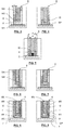
Figure 3 : représente la cellule mémoire selon un premier mode de réalisation partiellement agencée dans la cavité avant la réaction de la couche métallique M3 sur la couche d'oxyde métallique stoechiométrique 12. -
Figure 4 : représente la cellule mémoire de lafigure 3 , la couche métallique M3 ayant réagi sur la couche d'oxyde métallique stoechiométrique 12 pour former la couche d'oxyde métallique stoechiométrique 13 et la couche d"oxyde métallique sous stoechiométrique 12p. -
Figure 5 : représente la cellule mémoire de lafigure 4 lors de la formation du filament et des lignes de courant. -
Figures 6 et 7 : représentent la cellule mémoire partiellement agencée dans une cavité selon un deuxième mode de réalisation avant et après réaction de la couche métallique M3 sur la couche d'oxyde métallique stoechiométrique 12. -
Figures 8 et 9 : représentent la cellule mémoire selon un troisième mode de réalisation où l'élément mémoire est entièrement agencé dans une cavité d'un dispositif microélectronique. - Les dessins joints sont donnés à titre d'exemples et ne sont pas limitatifs de l'invention. Ils constituent des représentations schématiques de principe destinées à faciliter la compréhension de l'invention et ne sont pas nécessairement à l'échelle des applications pratiques. En particulier les épaisseurs relatives des différentes couches et films ne sont pas représentatives de la réalité.
- Avant d'entamer une revue détaillée de modes de réalisation de l'invention, sont énoncées ci-après des caractéristiques optionnelles qui peuvent éventuellement être utilisées en association ou alternativement.
- On rappelle tout d'abord que l'invention porte sur une cellule mémoire non volatile résistive comprenant un empilement comprenant deux électrodes et un isolant multi-couche, placé entre lesdites deux électrodes, comprenant une couche d'oxyde permettant une transition résistive et une couche de réservoir de lacunes d'oxygène caractérisée en ce que l'empilement comprend de bas en haut :
- une électrode inférieure comprenant une couche métallique M1,
- un isolant comprenant une couche d'oxyde métallique stoechiométrique 12 et une couche d'oxyde métallique sous stoechiométrique I2p formant ladite couche de réservoir de lacunes d'oxygène
- une électrode supérieure comprenant une couche d'oxyde métallique stoechiométrique 13 et une couche métallique M4, de sorte que la couche de réservoir de lacunes d'oxygène est intercalée entre deux couches d'oxydes métalliques stoechiométriques 12 et 13.
- Avantageusement, des métaux M2 et M3 respectivement pour former l'isolant 12 et I2p et pour former la couche d'oxyde métallique stoechiométrique 13 sont choisis de sorte que l'enthalpie libre de formation DG3 de l'oxyde métallique stoechiométrique 13 par oxydation du métal M3 est supérieure en valeur absolue à l'enthalpie libre de formation DG2 de l'oxyde métallique stoechiométrique 12 par oxydation du métal M2.
- Avantageusement, l'électrode inférieure comprend au-dessus de la couche métallique M1, une couche I1 d'oxyde métallique de M1.
- Avantageusement, les métaux M1et M3 sont choisis de sorte que l'enthalpie libre de formation DG1 de l'oxyde I1 par oxydation d'un métal M1 est supérieure ou égale en valeur absolue à l'enthalpie libre de formation DG3 de l'oxyde 13 par oxydation d'un métal M3.
- Avantageusement, le métal M1 est choisi de sorte que l'enthalpie libre de formation DG1 de l'oxyde I1 par oxydation d'un métal M1 est supérieure ou égale en valeur absolue à l'enthalpie libre de formation DG de la réaction 2Cu + 02 -> 2CuO.
- Avantageusement, les métaux M1 et M4 sont choisis parmi un métal non-noble autre que Pd, Ag, Ir, Pt, Au, ou un métal pure ou un alliage métallique binaire ou ternaire, ou un alliage à base de nitrure ou de carbure ou de siliciure ou d'oxyde métallique conducteur.
- Avantageusement, les métaux M1 et M4 sont choisis parmi TiN, TaN, TiAlN, TaAlN.
- Avantageusement, l'électrode inférieure et l'électrode supérieure sont symétriques dans l'empilement.
- Avantageusement, la couche I1 d'oxyde métallique stoechiométrique de M1 est choisie parmi Ti02 ou TiON ou Al2O3.
- Avantageusement, la couche d'oxyde stoechiométrique 12 est formée à partir d'un métal M2 choisi parmi des colonnes III, IV, V, du tableau périodique, ou AI ou Si, ou des lanthanides.
- Avantageusement, la couche d'oxyde stoechiométrique 12 est choisie parmi HfO2, ZrO2, TiO2, Al2O3, Ta2O5, Nb2O5, V2O5, La2O4, Gd2O3, Lu2O3, HfSiO, HfZrO, STO.
- Avantageusement, la couche d'oxyde stoechiométrique 12 d'un métal M2 présente une épaisseur de 1 à 50nm.
- Avantageusement, la couche d'oxyde métallique 13 est formée à partir d'un métal M3 choisi parmi, un métal pur ou un alliage métallique binaire ou ternaire.
- Avantageusement, le métal M3 est choisi parmi Si, Ti, Zr, Hf, AI, Ta, Nb, V, et les alliages en mélange de ces éléments, par exemple TiAI, TaAI.
- Avantageusement, l'empilement comprend de bas en haut : TiN/TiO2/Ta2O5/TaOx/TiO2/TiN, ou TiN/TiO2/Ta2O5/TaOx/Nb2O5/TiN, ou TiN/TiO2/V2O5/VOx/Nb2O5/TiN, ou TiN/TiO2/V2O5/VOx/Ta2O5/TiN
- Un autre objet de l'invention est un procédé de fabrication d'une cellule mémoire telle que décrites précédemment comprenant les étapes successives suivantes :
- Dépôt d'une couche métallique M1 pour former l'électrode inférieure,
- Dépôt d'une couche d'oxyde métallique stoechiométrique 12,
- Dépôt d'une couche métallique M3,
- Réaction de la couche métallique M3 avec l'oxyde métallique 12 formant un oxyde sous stoechiométrique I2p et un oxyde métallique stoechiométrique 13,
- Dépôt d'une couche métallique M4.
- Avantageusement, le dépôt de la couche métallique M3 est réalisé par dépôt flash en phase vapeur. Avantageusement, le dépôt de la couche métallique M3 n'est pas un dépôt conforme. Cela permet notamment de simplifier la réalisation.
- Avantageusement et optionnellement, la couche métallique M3 est déposée sur une épaisseur de 0,1 à 2nm.
- Avantageusement, la couche d'oxyde 12 métallique stoechiométrique est déposée par voie chimique.
- Avantageusement, la couche d'oxyde métallique stoechiométrique 12 est traitée au plasma ou par nitruration plasma.
- Avantageusement, la couche d'oxyde métallique stoechiométrique 12 est implantée d'aluminium.
- Un autre objet de l'invention est un dispositif microélectronique caractérisé en ce qu'il comprend une cellule mémoire telle que décrite ci-dessus.
- Avantageusement, le dispositif comprend une cavité dans laquelle est au moins partiellement agencée la cellule mémoire. La cavité est formée dans un matériau électriquement isolant, tel qu'un oxyde.
- Avantageusement, l'électrode inférieure de la cellule mémoire est agencée en dessous et en dehors de la cavité.
- Avantageusement, l'électrode inférieure de la cellule mémoire est agencée dans la cavité.
- Avantageusement, le dispositif comprend une pluralité de niveau d'interconnexion et une pluralité de plug de connexion entre les niveaux, chaque plug comprenant une cavité dans laquelle est au moins partiellement agencée une cellule mémoire telle que décrite ci-dessus.
- Un autre objet de l'invention est un procédé de fabrication d'un dispositif tel que décrit ci-dessus comprenant les étapes successives suivantes :
- Dépôt conforme d'une couche d'oxyde métallique stoechiométrique 12 dans la cavité,
- Dépôt d'une couche métallique M3 dans la cavité, de préférence par dépôt flash en phase vapeur. Ce dépôt de la couche métallique M3 est effectué sur la couche d'oxyde métallique stoechiométrique 12, de préférence dans le fond de la cavité de manière à ce qu'une portion des ou de la parois de la couche d'oxyde métallique stoechiométrique 12 ne soit pas recouverte par la couche métallique M3. ;
- Réaction de la couche métallique M3 avec l'oxyde métallique stoechiométrique 12 formant un oxyde sous stoechiométrique I2p et un oxyde métallique stoechiométrique 13,
- Dépôt d'au moins une couche métallique M4 dans la cavité. Ce dépôt de la couche métallique M4 est effectué sur l'oxyde métallique stoechiométrique 13 et sur la ou les parois verticales de la couche d'oxyde métallique stoechiométrique 12.
- Avantageusement, le procédé comprend le dépôt conforme d'une couche métallique M1 dans la cavité pour former l'électrode inférieure avant le dépôt de la couche d'oxyde métallique stoechiométrique 12.
- Avantageusement, le procédé comprend le dépôt d'une couche métallique M5 pour boucher la cavité.
- Avantageusement, le dépôt de la couche métallique M3 est réalisé par dépôt flash en phase vapeur.
- Avantageusement, la couche métallique M3 est déposée sur une épaisseur de 0,1 à 2nm.
- Avantageusement, la couche d'oxyde métallique stoechiométrique 12 est déposée par voie chimique.
- Avantageusement, la couche d'oxyde métallique stoechiométrique 12 est traitée au plasma ou par nitruration plasma.
- Avantageusement, la couche d'oxyde métallique stoechiométrique 12 est implantée d'aluminium.
- On notera que les caractéristiques relatives énoncées ci-dessus, notamment celles relatives à l'empilement de la cellule mémoire et à l'agencement de la cellule mémoire dans la cavité, bien qu'oeuvrant avantageusement en synergie lorsqu'elles sont combinées, peuvent être exploitées indépendamment les unes des autres et conférer néanmoins alors certains avantages techniques.
- Il est précisé que dans le cadre de la présente invention, le terme « sur », « surmonte » ou « sous-jacent » ou leurs équivalents ne signifient pas obligatoirement « au contact de ». Ainsi par exemple, le dépôt d'une première couche sur une deuxième couche, ne signifie pas obligatoirement que les deux couches sont directement au contact l'une de l'autre mais cela signifie que la première couche recouvre au moins partiellement la deuxième couche en étant soit directement à son contact soit en étant séparée d'elle par une autre couche ou un autre élément.
- On entend les termes « couche » et « film » comme des synonymes.
- On entend par « couche mince », une couche dont l'épaisseur varie de quelques couches atomiques à quelques micromètres.
- Par dispositif microélectronique, on entend tout type de dispositif réalisé avec des moyens de la microélectronique. Ces dispositifs englobent notamment en plus des dispositifs à finalité purement électronique, des dispositifs micromécaniques ou électromécaniques (MEMS, NEMS...) ainsi que des dispositifs optiques ou optoélectroniques (MOEMS...)
- La cellule mémoire selon l'invention est un empilement de couches de type Métal-Isolant-Métal (MIM) plus spécifiquement de type Métal-Oxyde-Métal (MOM). La cellule mémoire est une mémoire non volatile à changement de résistance. Les mémoires résistives (RRAM pour Resistive Random Access Memory) reposent sur le changement de résistance d'un matériau actif, plus précisément dans la sous-catégorie des OxRRAM (Oxyde RRAM) le matériau actif est un oxyde formant un isolant 2. Les deux couches métalliques de part et d'autres de l'isolant 2 sont des électrodes 1, 3.
- L'empilement selon un mode de réalisation préféré de l'invention est représenté à la
figure 1 . L'empilement comprend de bas en haut: une couche métallique M1, éventuellement une couche d'oxyde métallique 11, une couche d'oxyde métallique stoechiométrique 12, une couche d'oxyde métallique sous stoechiométrique I2p, une couche d'oxyde métallique stoechiométrique 13 et une couche métallique M4. - Une électrode inférieure 1 également appelée « bottom electrode » en anglais comprend la couche métallique M1 et par-dessus potentiellement une couche d'oxyde métallique I1.
- La couche métallique M1 est formée par un métal non noble. On entend par noble, un métal qui ne s'oxyde pas spontanément à l'air. Selon l'invention, les métaux nobles s'entendent de l'argent (Ag), de l'Iridium (Ir), du Platine (Pt), de l'or (Au) et du palladium (Pd). La couche métallique M1 peut-être un métal pure ou un alliage métallique binaire ou ternaire tel que par exemple TiAl, TaAl, TiAlN, TaAlN ou bien encore ou un alliage à base de nitrure, ou de carbure, ou de siliciure, ou d'oxyde métallique conducteur, préférentiellement TiN, TaN.
- L'oxyde métallique I1 est un oxyde qui peut se former lors du procédé de fabrication de la cellule mémoire. Le métal de la couche métallique M1 peut être oxydé par l'air en contact, ou bien par un oxyde métallique stoechiométrique 12 décrit ci-après. Selon une autre possibilité, la couche métallique M1 peut aussi être intentionnellement oxydée pour former l'oxyde métallique I1. Selon encore une autre possibilité, l'oxyde métallique I1 est déposé, par exemple pour former un sélecteur ou une diode résistance non-linéaire. .A titre d'exemple l'oxyde métallique I1 est du Ti02 ou du TiON.
- Un isolant 2 comprend avantageusement au moins deux couches de matériaux également appelé un multicouche, l'isolant 2 est préférentiellement une bi-couche. La bi-couche comprend une couche d'oxyde métallique stoechiométrique 12 et une couche d'oxyde métallique sous stoechiométrique I2p.
- Le terme stoechiométrique s'entend comme la proportion des éléments dans une formule brute. Une couche sous stoechiométrique selon l'invention présente une proportion d'oxygène inférieure à la proportion stoechiométrique du composé.
- L'oxyde métallique stoechiométrique 12 constitue la couche active présentant une variation résistive en fonction d'une tension appliquée. L'oxyde métallique sous stoechiométrique I2p constitue quant à lui une couche réservoir de lacunes d'oxygènes. Cette couche est un oxyde présentant une quantité d'oxygène moindre que l'oxyde stoechiométrique. Ce défaut d'oxygène est défini comme des lacunes en oxygène. Plus un matériau présente des lacunes d'oxygène, plus il est conducteur. Cette couche I2p de réserve de lacunes d'oxygène permet de faciliter les variations de résistivité de la couche d'oxyde 12. En effet, les deux couches 12 et I2p interagissent lors des phases de SET et de RESET de sorte permettre la formation des filaments conducteurs entre les deux électrodes 1 et 3.
- La couche d'oxyde métallique stoechiométrique 12 est avantageusement une couche mince.
- L'oxyde métallique stoechiométrique 12 est un oxyde stoechiométrique métallique. Cet oxyde 12 est choisi parmi des colonnes III, IV, V, du tableau périodique, ou Aluminium (Al) ou Silicium (Si), ou un lanthanide, à titre d'exemple Hf02, Zr02, Ti02, Al2O3, Ta2O5, Nb2O5, La2O4, Gd2O3, Lu2O3, ou des composés ternaires HfSiO, HfZrO, STO. L'oxyde métallique stoechiométrique 12 est préférentiellement du Ta2O5. Préférentiellement, la couche d'oxyde métallique stoechiométrique 12 est déposée par voie chimique. Avantageusement son épaisseur est comprise entre 1 nm et 50nm. Selon une possibilité, l'oxyde métallique stoechiométrique 12 est traité au plasma. Ce type de traitement permet de moduler l'épaisseur finale L et/ou le profil de déplétion en oxygène de la couche d'oxyde métallique sous stoechiométrique I2p. A titre d'exemple, des traitements de type nitruration plasma (plasma Radio-fréquence ou Micro-onde N2) à l'azote ou nitruration sous atmosphère réductrice typiquement en atmosphère hydrogénée N2+ H2. Selon une autre possibilité, la couche d'oxyde métallique stoechiométrique 12 est traitée par implantation. L'implantation peut être faite directement dans la couche 12 ou bien à travers la couche d'oxyde métallique stoechiométrique 13 et la couche d'oxyde métallique sous stoechiométrique 12p. Ce traitement par implantation permet de favoriser la formation de filaments conducteurs entre l'électrode inférieure 1 et l'électrode supérieure 3 de l'empilement de la cellule mémoire. A titre d'exemple, une implantation d'aluminium peut être réalisée.
- L'oxyde métallique I2p est un oxyde sous stoechiométrique. Cet oxyde I2p n'est pas volontairement déposé mais est issu d'une réaction avec un métal M3 déposé au-dessus de l'oxyde métallique stoechiométrique 12.
- Le métal M3 est préférentiellement un métal pur ou un alliage métallique binaire ou ternaire, par exemple, TiAl, TaAl, préférentiellement du Titane (Ti) pur.
- Selon un mode de réalisation préféré, le métal M3 est déposé par dépôt flash en phase vapeur (flash PVD en anglais). Le terme de « flash » correspond au contrôle sur un temps très court, avantageusement de l'ordre de la seconde, du dépôt d'un film de quelques Angstroem. Préférentiellement, la couche métallique M3 déposée est d'une épaisseur de 0,1nm à 2nm. Le contrôle de ce temps permet très avantageusement de déposer très précisément la quantité de métal M3 voulue afin de pouvoir moduler la profondeur de déplétion en oxygène dans la couche d'oxyde métallique stoechiométrique 12 et l'épaisseur finale L de la couche d'oxyde métallique sous stoechiométrique I2p.
- Le temps de flash va permettre de définir l'épaisseur finale de l'oxyde métallique stoechiométrique 13. Le type de dépôt du métal M3 influence la résistivité globale de la cellule mémoire. Selon un mode de réalisation, le dépôt flash permet de former des ilots localisés, appelés aussi dots, nanodots ou nanocristaux, permettant de réduire localement la couche d'oxyde métallique stoechiométrique 12, et ainsi permettre de localiser les filaments conducteurs 4 dans la couche d'oxyde métallique stoechiométrique 12.
- Le métal M3 déposé n'est plus présent sous forme de métal dans la cellule mémoire finalisée. Le métal M3 est configuré pour réagir avec la couche d'oxyde métallique stoechiométrique 12. Cette réaction conduit à une réduction partielle de l'oxyde métallique stoechiométrique 12 en un oxyde métallique sous stoechiométrique I2p et à l'oxydation du métal M3 en une couche d'oxyde métallique stoechiométrique 13. A titre d'exemple préféré, le métal M3 est du titane pur qui réagit avec l'oxyde métallique stoechiométrique I2,Ta2O5, pour former l'oxyde métallique stoechiométrique 13, Ti02, et l'oxyde métallique sous stoechiométrique I2p, Ta02. Cette réaction peut selon une possibilité être activée thermiquement.
- Avantageusement, la réduction de l'oxyde 12 par le métal M3 est possible si l'enthalpie libre de formation (DG3) de la réaction M3+O2->I3 est supérieure en valeur absolue à l'enthalpie libre de formation (DG2) de la réaction M2+O2->I2.Ceci peut se résumer par | DG3 | > | DG2|. Un abaque d'Elligham peut typiquement être utilisé afin de prévoir le sens des réactions.
- La quantité de métal M3 déposée est très faible au regard de l'épaisseur de 12 de sorte à ne pas consommer l'intégralité de oxyde métallique stoechiométrique 12 sans pouvoir obtenir le profil de déplétion d'oxygène visé dans l'oxyde métallique sous stoechiométrique 12p.
- Selon un mode de réalisation le métal M3 réduit la couche d'oxyde métallique stoechiométrique 12, mais pas une couche d'oxyde I1 possiblement présent à la surface de la couche métallique M1. De ce fait il est avantageux que l'enthalpie libre de formation (DG1) de la réaction M1+ 02 -> I1 soit supérieure ou égale en valeur absolue à l'enthalpie libre (DG3) de formation de la réaction M3+O2->I3 c'est-à-dire | DG1 | ≥ | DG3 | ou | DG1 | ≤ | DG(2Cu + 02 -> 2CuO) | c'est-à-dire l'enthalpie libre de formation DG1 de l'oxyde I1 par oxydation d'un métal M1 est supérieure ou égale en valeur absolue à l'enthalpie libre de formation DG de la réaction 2Cu+O2->2CuO.
- Une électrode supérieure 3 également appelée « top electrode » en anglais comprend la couche métallique M4 et une couche d'oxyde métallique stoechiométrique 13. La couche d'oxyde métallique 13 forme une couche isolant permettant d'isoler la couche métallique M4 formant partiellement l'électrode supérieure 3 de la couche d'oxyde métallique sous stoechiométrique I2p constituant la couche de réservoir de lacunes d'oxygène. La présence de cette couche isolante 13 permet de s'affranchir d'électrodes nobles ne risquant pas d'être oxydées.
- La couche métallique M4 est formée par un métal non noble. On entend par noble, un métal qui ne s'oxyde pas spontanément à l'air. Selon l'invention, les métaux nobles s'entendent de l'argent (Ag), de l'Iridium (Ir), du Platine (Pt), de l'or (Au) et du palladium (Pd). La couche métallique M4 peut être un métal pur ou un alliage métallique binaire ou ternaire tel que par exemple TiN, TaN, TiAlN, TaAlN ou bien encore ou un alliage à base de nitrure, ou de carbure, ou de siliciure, ou d'oxyde métallique conducteur, préférentiellement TiN, TaN.
- Selon un mode de réalisation préférée, l'électrode inférieure 1 et l'électrode supérieure 3 sont symétriques. On entend par symétrique que les deux électrodes 1 et 3 sont de même épaisseurs, de même propriétés, de même matériaux.
- Selon un exemple préféré, l'empilement de la cellule mémoire se compose de TiN/TiO2/Ta2O5/TaOx/TiO2/TiN, ou TiN/TiO2/Ta2O5/TaOx/Nb2O5/TiN, ou TiN/TiO2/V2O5/VOx/Nb2O5/TiN, ou TiN/TiO2/V2O5/VOx/Ta2O5/TiN
- Selon l'invention, un profil en oxygène tel qu'illustré en
figure 2 est particulièrement recherché. On peut voir sur cette figure que la couche d'oxyde métallique sous stoechiométrique I2p présente une déplétion en oxygène par rapport aux autres couches d'oxyde métallique stoechiométrique 11, 12 et 13 de l'empilement. On note LI2P l'épaisseur de l'oxyde métallique stoechiométrique 12, et petit II2P l'épaisseur du profil de déplétion. Le profil de déplétion est caractérisé par II2P<LI2P. - La présente invention concerne également un procédé de fabrication d'une cellule mémoire telle que décrite ci-dessus.
- Un tel procédé comprend un série d'étapes successives dont le dépôt de la couche métallique M1, puis le dépôt de l'oxyde métallique stoechiométrique 12 puis le dépôt d'une couche de métal M3 puis la formation de la couche d'oxyde métallique stoechiométrique 13 et de la couche métallique sous stoechiométrique 12p par réaction entre le métal M3 et l'oxyde stoechiométrique 12, puis le dépôt d'une couche métallique M4.
- La réaction entre la couche métallique M3 et l'oxyde métallique stoechiométrique 12 est avantageusement contrôlée par le choix des métaux M1, M2 et M3. Avantageusement, l'enthalpie libre de formation (DG3) de la réaction M3+O2->I3 est supérieure en valeur absolue à l'enthalpie libre de formation (DG2) de la réaction M2+O2->I2. Il est avantageux que l'enthalpie libre de formation (DG1) de la réaction M1+ 02 -> I1 soit supérieure ou égale en valeur absolue à l'enthalpie libre (DG3) de formation de la réaction M3+O2->I3.
- Avantageusement, la couche métallique M3 réduit la couche d'oxyde métallique stoechiométrique 12, mais pas une couche d'oxyde stoechiométrique I1 possiblement présent à la surface de la couche métallique M1.
- Une cellule mémoire selon l'invention peut être intégrée dans divers dispositif microélectronique allant de dispositifs de stockage de données portables à des structures mémoires neuro-morphiques.
- L'intégration des films actifs d'une cellule mémoire selon l'invention telle que décrite ci-dessus, se fait actuellement dans les lignes Back-End des dispositifs microélectroniques utilisant des cellules mémoires, à un niveau métal Mi, l'indice i étant un entier qui représente le nombre de niveaux d'interconnexion dans un dispositif. Ces films sont déposés en planaire à la surface d'un plug. Ensuite, une étape de gravure permet de définir la taille finale de la cellule mémoire. Enfin, un nouveau plug est créé à l'étage supérieur (Mi+1) et vient connecter l'électrode supérieure de la cellule mémoire. La formation d'un plug requiert, le dépôt d'un oxyde à basse température, la gravure d'un trou aligné sur l'électrode supérieure, puis le dépôt dans ce trou d'un métal de contact, typiquement TiN/W ou Ta/TaN/Cu.
- Le dépôt de l'oxyde basse température amène de l'oxygène exogène en contact de la cellule mémoire et engendre une détérioration des propriétés de la cellule. On connait du document
US2014/0197368 la possibilité de limiter l'impact de l'oxygène exogène amené par l'étape de dépôt de l'oxyde basse température, en déposant un film conforme de SiN par voie CVD après la gravure de l'élément mémoire déposé en planaire Ce film permet de « sceller » les flancs de la cellule mémoire. Ce type de capping à l'oxygène avec SiN est très utilisé pour les transistors CMOS. Toutefois, avec la réduction de taille des dispositifs, ce film de SiN subit aussi une réduction d'épaisseur afin de suivre la géométrie globale des dispositifs. Par exemple dans les lignes des niveaux Mi, l'épaisseur du niveau représente environ 2 à 3 fois la largeur du plug. Ceci afin de respecter un aspect ratio raisonnable pour les plugs afin d'assurer un remplissage optimal des plugs en voie chimique CVD. L'épaisseur minimum du film de SiN proposé dans ce document est de 20nm. Dans le cas où l'élément mémoire présente une taille de l'ordre ou inférieur à 40nm, on s'aperçoit qu'un film de 20nm représente environ 1/3 de la hauteur du niveau Mi. Or, en-dessous d'une certaine épaisseur de SiN d'environ 20nm, le procédé de dépôt plasma de Si02 impacte les films sous-jacents. Effectivement, le plasma de traitement utilisé in-situ au cours du dépôt de l'isolant inter-plugs est physiquement pénétrant et des espèces de type O* peuvent passer au travers du film de protection en SiN. - Il existe donc le besoin de proposer une technologie qui permet de limiter l'impact de l'oxygène exogène amené par l'étape de dépôt de l'oxyde basse température lors de la formation d'un plug.
- Selon un autre aspect de l'invention, la cellule mémoire telle que décrite ci-dessus peut être agencée au moins partiellement dans une cavité 6 aussi dénommée « via ».
- Avantageusement, l'invention trouvera également son application pour des dispositifs micro-électroniques et nanoélectroniques comprenant une pluralité de niveaux d'interconnexion et une pluralité de plugs de connexion entre les niveaux. Chaque plug comprend une cavité 6. Selon l'invention, la cavité 6 possède une largeur 8 d'ouverture inférieure à 180nm, préférentiellement égale ou inférieure à 65 nm.
- La cavité 6 est formée dans de l'oxyde de Si02 déposé par voie chimique pour former un plug d'interconnexion débouchant sur une ligne de connexion 7 de niveau inférieure Mi-1. Plus généralement la cavité 6 est formée dans un matériau électriquement isolant.
- Selon un premier mode de réalisation illustré aux
figures 3 à 7 , l'empilement de la cellule mémoire est partiellement agencé dans la cavité 6. La ligne de connexion 7 du niveau inférieur Mi-1 forme la couche métallique M1 et éventuellement sa couche d'oxyde métallique stoechiométrique I1. Cela est possible lorsque la ligne de connexion 7 est en Al, Ta, TaN ou TiN. La couche d'oxyde métallique stoechiométrique I1 est alors en Al2O3, Ti02, TiON, Ta2O5, TaON. La couche métallique M1 de l'électrode inférieure 1 et éventuellement la couche d'oxyde métallique stoechiométrique I1 sont disposées en dehors et sous la cavité. On entend par dessous que la couche métallique M1 est présente avant la formation de la cavité, et on entend par en dehors, que la couche métallique M1 est d'une longueur plus importante que la largeur de la cavité 6. - La cavité 6 comprend de bas en haut, l'isolant 2 comprenant la couche d'oxyde métallique stoechiométrique 12 et la couche d'oxyde métallique sous stoechiométrique I2p formant ladite couche de réservoir de lacunes d'oxygène puis la couche d'oxyde métallique stoechiométrique 13 et la couche métallique M4.
- Selon cet empilement, la couche d'oxyde métallique stoechiométrique I1 est avantageusement présente pour maintenir la couche d'oxyde métallique sous-stoechiométrie I2p en contact de couches d'oxyde métallique stoechiométrique 11, 12 et 13.
- Selon un deuxième mode de réalisation illustré aux
figures 8 et 9 , l'empilement de la cellule mémoire est entièrement agencé dans la cavité 6. La ligne de connexion 7 du niveau inférieur Mi-1 ne forme pas la couche métallique M1. Cela est le cas notamment lorsque la ligne de connexion 7 est en un matériau non adapté aux propriétés nécessaires pour former une électrode inférieure 1. La couche métallique M1 de l'électrode inférieure 1 et éventuellement la couche d'oxyde métallique stoechiométrique I1 sont disposées dans la cavité 6. Dans cette réalisation, on note que l'isolant 2 formé au moins par la couche d'oxyde métallique stoechiométrique 12 conforme garantit l'isolation électrique entre les couches métalliques M1 et M4. La couche métallique M1 joue alors le rôle de barrière destinée à limiter la diffusion du matériau de la ligne de connexion 7 dans la cellule mémoire. - Le procédé de fabrication d'une cellule mémoire comprend les étapes décrites ci-après. La formation d'une cavité 6 débouchant sur une ligne de connexion 7 de niveau inférieur Mi-1. Eventuellement, le dépôt conforme d'une couche métallique M1 dans la cavité 6. Eventuellement, le dépôt conforme ou la formation d'une couche d'oxyde métallique stoechiométrique I1 au contact de la couche métallique M1. Le dépôt conforme d'une couche d'oxyde métallique stoechiométrique 12. Avantageusement, le dépôt de la couche d'oxyde métallique stoechiométrique 12 est effectué par dépôt chimique en phase vapeur (acronyme CVD). On entend par dépôt conforme que le dépôt est effectué en fond et sur les parois de la cavité 6. Le dépôt d'une couche de métal M3 en fond de cavité, préférentiellement déposée par dépôt flash physique en phase vapeur (acronyme PVD), par exemple en flash Ti, Al, Zr, Hf, Si, Ta, Nb, V. Le procédé comprend une étape de bouchage de la cavité 6. Au moins une couche métallique M4 est déposée dans la cavité 6. La couche métallique M4 est avantageusement imperméable à l'oxygène tel que par exemple Co, Ni, Cu. Les dépôts des couches métalliques M1 et M4 sont avantageusement réalisés comme pour l'empilement illustré en
figure 1 . - La réaction de la couche métallique M3 sur l'oxyde métallique stoechiométrique 12 résulte en la formation de l'oxyde sous-stoechiométrique I2p localisé autour, plus précisément à proximité immédiate, de la couche d'oxyde métallique stoechiométrique 13. Cette réaction peut être assistée par recuit typiquement aligné sur le recuit du Back End à environ 400°C. Dans cette réalisation, la couche sensible à l'oxygène exogène I2p se retrouve enterrée en fond de cavité 6, protégée de l'oxydation par des couches isolantes : l'oxyde métallique stoechiométrique 12 résiduel (i.e. n'ayant pas réagi) et l'oxyde métallique stoechiométrique 13 et la couche métallique M4.
- Selon l'invention, le procédé comprend une étape de dé-contact des plugs d'un même niveau comprenant un polissage mécano-chimique (acronyme CMP). Lors du dépôt des couches d'oxyde métallique stoechiométrique 12 et métallique M4, de la matière reste potentiellement en dehors de la cavité 6. Cette matière peut entrainer une conduction entre les différentes cavités 6 du niveau dans le dispositif.
- Avantageusement, la couche d'oxyde métallique stoechiométrique 12 présente une largeur L comprise entre 2 et 20 nm. Cette largeur L s'entend comme la dimension séparant les parois de la cavité 6 de la couche d'oxyde métallique stoechiométrique 13.
- Avantageusement, la couche d'oxyde métallique stoechiométrique 13 présente une largeur I comprise entre 10 et 40 nm, préférentiellement 25nm.
- Par exemple, pour une cavité de 45nm, largeur L de la couche d'oxyde métallique stoechiométrique 12 est de 10nm et largeur I de la couche d'oxyde métallique stoechiométrique 13 est de 25nm.
- Cette disposition d'empilement permet de de confiner/localiser le filament de lacunes sous la couche d'oxyde métallique stoechiométrique 13 de largeur I. De plus, les lignes de courant sont localisées dans une zone limitée augmentant l'échauffement local. Cette constriction des lignes de courant permet de réduire le potentiel de formation du filament Vf. Le potentiel de formation Vf est avantageusement inférieur à 3V et préférentiellement de l'ordre de 2V autorisant ainsi l'intégration de la cellule mémoire selon l'invention dans des dispositifs CMOS. L'invention présente également l'avantage de réduire la variabilité de l'état passant, Ron, de la cellule mémoire.
- Selon une autre possibilité, le bouchage de la cavité peut être réalisé par l'empilement de plusieurs couches. Tel qu'illustré en
figures 6 à 9 , deux couches métalliques M4 et M5 sont déposées dans la cavité 6 pour la boucher. La couche métallique M4 pouvant être du TiN ou TaN . La couche métallique M5 est un métal imperméable à l'oxygène tel que du Cobalt, du Nickel ou du Cuivre. Dans cette disposition, le procédé de fabrication comprend une étape de déconnection des couches métalliques M1 et M5, avantageusement par CMP. - Cet empilement de la cellule mémoire au moins partiellement dans une cavité peut s'applique au domaine des mémoires CBRam dans lesquelles la modulation de la résistance de l'isolant 2 est réalisée par un filament par exemple de Cuivre dans le cas où la couche métallique M4 est du Cuivre. Ce type de mémoire peut servir à réaliser de structures mémoires du type neuro-morphique.
-
- 1.
- Electrode inférieure
- 2.
- Isolant
- 3.
- Électrode supérieure
- 4.
- Filament
- 5.
- Lignes de courant
- 6.
- Cavité
- 7.
- Ligne de connexion
- 8.
- Largeur d'ouverture de la cavitéM1. Couche métallique
- I1.
- Couche d'oxyde métallique
- I2.
- Couche d'oxyde métallique stoechiométrique
- I2p.
- Couche d'oxyde métallique sous stoechiométrique
- I3.
- Couche d'oxyde métallique stoechiométrique
- M4.
- Couche d'oxyde métallique
- LI2P.
- Epaisseur finale de la couche d'oxyde sous stoechiométrique I2p
- II2P.
- Epaisseur du profil de déplétion
- I.
- Largeur de la couche d'oxyde métallique stoechiométrique 13
- L.
- Largeur de la couche d'oxyde métallique stoechiométrique 12
Claims (16)
- Cellule mémoire non volatile résistive comprenant un empilement comprenant deux électrodes (1, 3) et un isolant (2) multi-couche, placé entre lesdites deux électrodes (1, 3), l'isolant (2) multi-couche comprenant une couche d'oxyde permettant une transition résistive et une couche de réservoir de lacunes d'oxygène, caractérisée en ce que l'empilement comprend de bas en haut :- une électrode inférieure (1) comprenant une couche métallique M1,- l'isolant (2) comprenant une couche d'oxyde métallique stoechiométrique 12 et une couche d'oxyde métallique sous stoechiométrique I2p formant ladite couche de réservoir de lacunes d'oxygène,- une électrode supérieure (3) comprenant une couche d'oxyde métallique stoechiométrique 13 et une couche métallique M4, de sorte que la couche de réservoir de lacunes d'oxygène est intercalée entre deux couches d'oxydes métalliques stoechiométriques 12 et 13.
- Cellule mémoire selon la revendication 1 dans laquelle des métaux M2 et M3 sont choisis de sorte que l'enthalpie libre de formation DG3 de l'oxyde métallique stoechiométrique 13 par oxydation du métal M3 est supérieure en valeur absolue à l'enthalpie libre de formation DG2 de l'oxyde métallique stoechiométrique 12 par oxydation du métal M2.
- Cellule mémoire selon l'une quelconque des revendications précédentes dans laquelle l'électrode inférieure (1) comprend au-dessus de la couche métallique M1, une couche I1 d'oxyde métallique stoechiométrique de M1, et de préférence dans laquelle des métaux M1 et M3 sont choisis de sorte que l'enthalpie libre de formation DG1 de l'oxyde métallique stoechiométrique I1 par oxydation du métal M1 est supérieure ou égale en valeur absolue à l'enthalpie libre de formation DG3 de l'oxyde métallique stoechiométrique 13 par oxydation du métal M3.
- Cellule mémoire selon l'une quelconque des revendications précédentes dans laquelle les couches métalliques M1 et M4 sont formées par au moins un métal parmi un métal non-noble autre que Pd, Ag, Ir, Pt, Au, et de préférence dans laquelle les métaux des couches métalliques M1 et M4 sont un métal pur ou un alliage métallique binaire ou ternaire, ou un alliage à base de nitrure ou de carbure ou de siliciure ou d'oxyde métallique conducteur et de préférence dans laquelle les métaux M1 et M4 sont choisis parmi TiN, TaN, TiAlN, TaAlN.
- Cellule mémoire selon l'une quelconque des revendications précédentes en combinaison de la revendication 3 dans laquelle la couche d'oxyde métallique stoechiométrique I1 de la couche métallique M1 est choisie parmi Ti02 ou TiON ou Al2O3.
- Cellule mémoire selon l'une quelconque des revendications précédentes en combinaison de la revendication 3 dans laquelle la couche d'oxyde stoechiométrique 12 d'un métal M2 est choisi parmi des colonnes III, IV, V, du tableau périodique, ou Al ou Si, ou des lanthanides, et de préférence dans laquelle la couche d'oxyde stoechiométrique 12 est choisie parmi Hf02, Zr02, Ti02, Al2O3, Ta2O5, Nb2O5, V2O5,La2O4, Gd2O3, Lu2O3, HfSiO, HfZrO, STO.
- Cellule mémoire selon l'une quelconque des revendications précédentes dans laquelle le métal M3 formant la couche d'oxyde métallique 13 est un métal pur ou un alliage métallique binaire ou ternaire, et de préférence dans laquelle le métal M3 est choisi parmi Si, Ti, Zr, Hf, Al, Ta, Nb, V, et les alliages en mélange de ces éléments par exemple TiAl, TaAl.
- Cellule mémoire selon l'une quelconque des revendications précédentes dans laquelle l'empilement comprend de bas en haut : TiN/TiO2/Ta2O5/TaOx/TiO2/TiN.
- Dispositif microélectronique comprenant une cavité (6) dans laquelle est au moins partiellement agencée une cellule mémoire selon l'une quelconque des revendications précédentes.
- Dispositif selon la revendication précédente dans laquelle l'électrode inférieure (1) de la cellule mémoire est agencée en dessous et en dehors de la cavité (6) ou dans laquelle l'électrode inférieure (1) de la cellule mémoire est agencée dans la cavité (6) et dans laquelle la couche d'oxyde stoechiométrique 12 présente de préférence une épaisseur de 1 à 50nm.
- Dispositif selon l'une quelconque des deux revendications précédentes comprenant une pluralité de niveau d'interconnexion et une pluralité de plug de connexion entre les niveaux, chaque plug comprenant une cavité (6) dans laquelle est au moins partiellement agencée une cellule mémoire selon l'une quelconque des revendications 1 à 8.
- Procédé de fabrication d'une cellule mémoire selon l'une quelconque des revendications 1 à 8 ou d'un dispositif microélectronique selon l'une quelconque des revendications 9 à 11 comprenant les étapes successives suivantes :- Dépôt d'une couche métallique M1 pour former l'électrode inférieure (1),- Dépôt d'une couche d'oxyde métallique stoechiométrique 12,- Dépôt d'une couche métallique M3,- Réaction de la couche métallique M3 avec l'oxyde métallique stoechiométrique 12 formant un oxyde sous stoechiométrique I2p et un oxyde métallique stoechiométrique 13,- Dépôt d'une couche métallique M4.
- Procédé selon la revendication précédente dans lequel le dépôt de la couche métallique M3 est réalisé par dépôt flash en phase vapeur et dans lequel la couche métallique M3 est déposée de préférence sur une épaisseur de 0,1 à 2 nm.
- Procédé selon l'une quelconque des deux revendications précédentes dans lequel la couche d'oxyde métallique stoechiométrique 12 est déposée par voie chimique et de préférence dans lequel la couche d'oxyde métallique stoechiométrique 12 est traitée au plasma ou par nitruration plasma.
- Procédé selon l'une quelconque des trois revendications précédentes dans lequel la couche d'oxyde métallique stoechiométrique 12 est implantée d'aluminium.
- Procédé de fabrication d'un dispositif selon l'une quelconque des revendications 9 à 11, comprenant les étapes successives suivantes :- Dépôt conforme d'une couche d'oxyde métallique stoechiométrique 12 dans la cavité (6),- Dépôt d'une couche métallique M3 dans la cavité (6),- Réaction de la couche métallique M3 avec l'oxyde métallique stoechiométrique 12 formant un oxyde sous stoechiométrique I2p et un oxyde métallique stoechiométrique 13,- Dépôt d'au moins une couche métallique M4 dans la cavité (6) ;et, de préférence, comprenant avant l'étape de dépôt de la couche d'oxyde métallique stoechiométrique 12, une étape de dépôt conforme d'une couche métallique M1 dans la cavité (6) pour former l'électrode inférieure (1).
Applications Claiming Priority (1)
| Application Number | Priority Date | Filing Date | Title |
|---|---|---|---|
| FR1550049A FR3031416B1 (fr) | 2015-01-06 | 2015-01-06 | Cellule memoire non volatile resistive et son procede de fabrication |
Publications (2)
| Publication Number | Publication Date |
|---|---|
| EP3043396A1 true EP3043396A1 (fr) | 2016-07-13 |
| EP3043396B1 EP3043396B1 (fr) | 2018-06-06 |
Family
ID=54065936
Family Applications (1)
| Application Number | Title | Priority Date | Filing Date |
|---|---|---|---|
| EP16150341.2A Not-in-force EP3043396B1 (fr) | 2015-01-06 | 2016-01-06 | Cellule mémoire non volatile résistive et son procédé de fabrication |
Country Status (3)
| Country | Link |
|---|---|
| US (1) | US9768379B2 (fr) |
| EP (1) | EP3043396B1 (fr) |
| FR (1) | FR3031416B1 (fr) |
Families Citing this family (7)
| Publication number | Priority date | Publication date | Assignee | Title |
|---|---|---|---|---|
| US9754665B2 (en) * | 2016-01-29 | 2017-09-05 | Sandisk Technologies Llc | Vacancy-modulated conductive oxide resistive RAM device including an interfacial oxygen source layer |
| US9887351B1 (en) | 2016-09-30 | 2018-02-06 | International Business Machines Corporation | Multivalent oxide cap for analog switching resistive memory |
| KR102578854B1 (ko) | 2016-12-31 | 2023-09-19 | 에스케이하이닉스 주식회사 | 저항성 메모리 소자 및 이의 제조 방법 |
| US10497752B1 (en) | 2018-05-11 | 2019-12-03 | International Business Machines Corporation | Resistive random-access memory array with reduced switching resistance variability |
| US10727407B2 (en) | 2018-08-08 | 2020-07-28 | International Business Machines Corporation | Resistive switching memory with replacement metal electrode |
| FR3103633B1 (fr) * | 2019-11-21 | 2023-05-26 | Commissariat Energie Atomique | Cellule mémoire de type OxRAM à faible tension de forming, et procédé de fabrication associé |
| CN114284431A (zh) * | 2021-12-23 | 2022-04-05 | 中国科学院微电子研究所 | 一种储备池元件的制备方法 |
Citations (3)
| Publication number | Priority date | Publication date | Assignee | Title |
|---|---|---|---|---|
| US20120032132A1 (en) * | 2010-08-06 | 2012-02-09 | Samsung Electronics Co., Ltd. | Nonvolatile Memory Elements And Memory Devices Including The Same |
| US20130146829A1 (en) * | 2011-12-12 | 2013-06-13 | Samsung Electronics Co., Ltd. | Resistive random access memory devices and methods of manufacturing the same |
| US20140197368A1 (en) | 2011-09-16 | 2014-07-17 | Panasonic Corporation | Nonvolatile memory element, nonvolatile memory device, nonvolatile memory element manufacturing method, and nonvolatile memory device manufacturing method |
Family Cites Families (6)
| Publication number | Priority date | Publication date | Assignee | Title |
|---|---|---|---|---|
| US7791925B2 (en) | 2008-10-31 | 2010-09-07 | Seagate Technology, Llc | Structures for resistive random access memory cells |
| JP4592828B2 (ja) * | 2009-02-04 | 2010-12-08 | パナソニック株式会社 | 不揮発性記憶素子 |
| KR101744758B1 (ko) * | 2010-08-31 | 2017-06-09 | 삼성전자 주식회사 | 비휘발성 메모리요소 및 이를 포함하는 메모리소자 |
| JP2014103326A (ja) * | 2012-11-21 | 2014-06-05 | Panasonic Corp | 不揮発性記憶素子およびその製造方法 |
| US9680095B2 (en) * | 2013-03-13 | 2017-06-13 | Macronix International Co., Ltd. | Resistive RAM and fabrication method |
| KR102275565B1 (ko) | 2014-03-25 | 2021-07-12 | 인텔 코포레이션 | 비평면 저항성 메모리 셀들을 형성하는 기법들 |
-
2015
- 2015-01-06 FR FR1550049A patent/FR3031416B1/fr not_active Expired - Fee Related
-
2016
- 2016-01-06 EP EP16150341.2A patent/EP3043396B1/fr not_active Not-in-force
- 2016-01-06 US US14/989,300 patent/US9768379B2/en not_active Expired - Fee Related
Patent Citations (3)
| Publication number | Priority date | Publication date | Assignee | Title |
|---|---|---|---|---|
| US20120032132A1 (en) * | 2010-08-06 | 2012-02-09 | Samsung Electronics Co., Ltd. | Nonvolatile Memory Elements And Memory Devices Including The Same |
| US20140197368A1 (en) | 2011-09-16 | 2014-07-17 | Panasonic Corporation | Nonvolatile memory element, nonvolatile memory device, nonvolatile memory element manufacturing method, and nonvolatile memory device manufacturing method |
| US20130146829A1 (en) * | 2011-12-12 | 2013-06-13 | Samsung Electronics Co., Ltd. | Resistive random access memory devices and methods of manufacturing the same |
Non-Patent Citations (1)
| Title |
|---|
| GYEONG-SU PARK: "ln situ observation of filamentary conducting channels in an asymmetric Ta205-x/Ta02-x bilayer structure", NATURE COMMUNICATIONS, vol. 4, 2013, pages 2382 |
Also Published As
| Publication number | Publication date |
|---|---|
| FR3031416A1 (fr) | 2016-07-08 |
| US20160197271A1 (en) | 2016-07-07 |
| EP3043396B1 (fr) | 2018-06-06 |
| FR3031416B1 (fr) | 2018-09-07 |
| US9768379B2 (en) | 2017-09-19 |
Similar Documents
| Publication | Publication Date | Title |
|---|---|---|
| EP3043396B1 (fr) | Cellule mémoire non volatile résistive et son procédé de fabrication | |
| EP2209139B1 (fr) | Elément de mémoire non volatile et dispositif semi-conducteur non volatile utilisant l'élément de mémoire non volatile | |
| US9570682B2 (en) | Semiconductor memory device and method of manufacturing the same | |
| KR101127236B1 (ko) | 저항성 메모리 소자의 제조 방법 | |
| US9385164B2 (en) | Method of making a resistive random access memory device with metal-doped resistive switching layer | |
| KR100913395B1 (ko) | 메모리 소자 및 그 제조방법 | |
| US8956939B2 (en) | Method of making a resistive random access memory device | |
| US8445883B2 (en) | Nonvolatile semiconductor memory device and manufacturing method thereof | |
| CN102648522B (zh) | 非易失性存储元件及其制造方法、以及非易失性存储装置 | |
| CN102217067B (zh) | 非易失性存储装置及其制造方法 | |
| CN103222055B (zh) | 非易失性存储元件及其制造方法 | |
| JP5436674B2 (ja) | 不揮発性記憶装置の製造方法 | |
| FR2969382A1 (fr) | Élément memristif et mémoire électronique basée sur de tels éléments | |
| US20140361235A1 (en) | Nonvolatile Resistive Memory Element With A Metal Nitride Containing Switching Layer | |
| EP4175448B1 (fr) | Procede de co-fabrication d'une memoire ferroelectrique et d'une memoire resistive oxram et dispositif co-integrant une memoire ferroelectrique et une memoire resistive oxram | |
| CN102244193A (zh) | 包含钌掺杂的氧化钽基电阻型存储器及其制备方法 | |
| KR101925448B1 (ko) | 가변 저항 메모리 장치 및 그 제조 방법 | |
| JP5232935B2 (ja) | 抵抗変化素子の製造方法 | |
| EP3984073B1 (fr) | Procédé de fabrication d'une cellule mémoire résistive de type oxram | |
| KR20110020886A (ko) | 저항성 메모리 소자의 제조 방법 | |
| EP3984072A1 (fr) | Procédé de détermination d'un paramètre de fabrication d'une cellule de mémoire vive résistive |
Legal Events
| Date | Code | Title | Description |
|---|---|---|---|
| PUAI | Public reference made under article 153(3) epc to a published international application that has entered the european phase |
Free format text: ORIGINAL CODE: 0009012 |
|
| AK | Designated contracting states |
Kind code of ref document: A1 Designated state(s): AL AT BE BG CH CY CZ DE DK EE ES FI FR GB GR HR HU IE IS IT LI LT LU LV MC MK MT NL NO PL PT RO RS SE SI SK SM TR |
|
| AX | Request for extension of the european patent |
Extension state: BA ME |
|
| STAA | Information on the status of an ep patent application or granted ep patent |
Free format text: STATUS: REQUEST FOR EXAMINATION WAS MADE |
|
| 17P | Request for examination filed |
Effective date: 20170113 |
|
| RBV | Designated contracting states (corrected) |
Designated state(s): AL AT BE BG CH CY CZ DE DK EE ES FI FR GB GR HR HU IE IS IT LI LT LU LV MC MK MT NL NO PL PT RO RS SE SI SK SM TR |
|
| GRAP | Despatch of communication of intention to grant a patent |
Free format text: ORIGINAL CODE: EPIDOSNIGR1 |
|
| STAA | Information on the status of an ep patent application or granted ep patent |
Free format text: STATUS: GRANT OF PATENT IS INTENDED |
|
| INTG | Intention to grant announced |
Effective date: 20171222 |
|
| GRAS | Grant fee paid |
Free format text: ORIGINAL CODE: EPIDOSNIGR3 |
|
| GRAA | (expected) grant |
Free format text: ORIGINAL CODE: 0009210 |
|
| STAA | Information on the status of an ep patent application or granted ep patent |
Free format text: STATUS: THE PATENT HAS BEEN GRANTED |
|
| AK | Designated contracting states |
Kind code of ref document: B1 Designated state(s): AL AT BE BG CH CY CZ DE DK EE ES FI FR GB GR HR HU IE IS IT LI LT LU LV MC MK MT NL NO PL PT RO RS SE SI SK SM TR |
|
| REG | Reference to a national code |
Ref country code: GB Ref legal event code: FG4D Free format text: NOT ENGLISH |
|
| REG | Reference to a national code |
Ref country code: CH Ref legal event code: EP Ref country code: AT Ref legal event code: REF Ref document number: 1007013 Country of ref document: AT Kind code of ref document: T Effective date: 20180615 |
|
| REG | Reference to a national code |
Ref country code: IE Ref legal event code: FG4D Free format text: LANGUAGE OF EP DOCUMENT: FRENCH |
|
| REG | Reference to a national code |
Ref country code: DE Ref legal event code: R096 Ref document number: 602016003233 Country of ref document: DE |
|
| REG | Reference to a national code |
Ref country code: NL Ref legal event code: MP Effective date: 20180606 |
|
| REG | Reference to a national code |
Ref country code: LT Ref legal event code: MG4D |
|
| PG25 | Lapsed in a contracting state [announced via postgrant information from national office to epo] |
Ref country code: BG Free format text: LAPSE BECAUSE OF FAILURE TO SUBMIT A TRANSLATION OF THE DESCRIPTION OR TO PAY THE FEE WITHIN THE PRESCRIBED TIME-LIMIT Effective date: 20180906 Ref country code: NO Free format text: LAPSE BECAUSE OF FAILURE TO SUBMIT A TRANSLATION OF THE DESCRIPTION OR TO PAY THE FEE WITHIN THE PRESCRIBED TIME-LIMIT Effective date: 20180906 Ref country code: FI Free format text: LAPSE BECAUSE OF FAILURE TO SUBMIT A TRANSLATION OF THE DESCRIPTION OR TO PAY THE FEE WITHIN THE PRESCRIBED TIME-LIMIT Effective date: 20180606 Ref country code: LT Free format text: LAPSE BECAUSE OF FAILURE TO SUBMIT A TRANSLATION OF THE DESCRIPTION OR TO PAY THE FEE WITHIN THE PRESCRIBED TIME-LIMIT Effective date: 20180606 Ref country code: CY Free format text: LAPSE BECAUSE OF FAILURE TO SUBMIT A TRANSLATION OF THE DESCRIPTION OR TO PAY THE FEE WITHIN THE PRESCRIBED TIME-LIMIT Effective date: 20180606 Ref country code: ES Free format text: LAPSE BECAUSE OF FAILURE TO SUBMIT A TRANSLATION OF THE DESCRIPTION OR TO PAY THE FEE WITHIN THE PRESCRIBED TIME-LIMIT Effective date: 20180606 Ref country code: SE Free format text: LAPSE BECAUSE OF FAILURE TO SUBMIT A TRANSLATION OF THE DESCRIPTION OR TO PAY THE FEE WITHIN THE PRESCRIBED TIME-LIMIT Effective date: 20180606 |
|
| PG25 | Lapsed in a contracting state [announced via postgrant information from national office to epo] |
Ref country code: LV Free format text: LAPSE BECAUSE OF FAILURE TO SUBMIT A TRANSLATION OF THE DESCRIPTION OR TO PAY THE FEE WITHIN THE PRESCRIBED TIME-LIMIT Effective date: 20180606 Ref country code: RS Free format text: LAPSE BECAUSE OF FAILURE TO SUBMIT A TRANSLATION OF THE DESCRIPTION OR TO PAY THE FEE WITHIN THE PRESCRIBED TIME-LIMIT Effective date: 20180606 Ref country code: HR Free format text: LAPSE BECAUSE OF FAILURE TO SUBMIT A TRANSLATION OF THE DESCRIPTION OR TO PAY THE FEE WITHIN THE PRESCRIBED TIME-LIMIT Effective date: 20180606 Ref country code: GR Free format text: LAPSE BECAUSE OF FAILURE TO SUBMIT A TRANSLATION OF THE DESCRIPTION OR TO PAY THE FEE WITHIN THE PRESCRIBED TIME-LIMIT Effective date: 20180907 |
|
| REG | Reference to a national code |
Ref country code: AT Ref legal event code: MK05 Ref document number: 1007013 Country of ref document: AT Kind code of ref document: T Effective date: 20180606 |
|
| PG25 | Lapsed in a contracting state [announced via postgrant information from national office to epo] |
Ref country code: NL Free format text: LAPSE BECAUSE OF FAILURE TO SUBMIT A TRANSLATION OF THE DESCRIPTION OR TO PAY THE FEE WITHIN THE PRESCRIBED TIME-LIMIT Effective date: 20180606 |
|
| PG25 | Lapsed in a contracting state [announced via postgrant information from national office to epo] |
Ref country code: PL Free format text: LAPSE BECAUSE OF FAILURE TO SUBMIT A TRANSLATION OF THE DESCRIPTION OR TO PAY THE FEE WITHIN THE PRESCRIBED TIME-LIMIT Effective date: 20180606 Ref country code: IS Free format text: LAPSE BECAUSE OF FAILURE TO SUBMIT A TRANSLATION OF THE DESCRIPTION OR TO PAY THE FEE WITHIN THE PRESCRIBED TIME-LIMIT Effective date: 20181006 Ref country code: EE Free format text: LAPSE BECAUSE OF FAILURE TO SUBMIT A TRANSLATION OF THE DESCRIPTION OR TO PAY THE FEE WITHIN THE PRESCRIBED TIME-LIMIT Effective date: 20180606 Ref country code: CZ Free format text: LAPSE BECAUSE OF FAILURE TO SUBMIT A TRANSLATION OF THE DESCRIPTION OR TO PAY THE FEE WITHIN THE PRESCRIBED TIME-LIMIT Effective date: 20180606 Ref country code: RO Free format text: LAPSE BECAUSE OF FAILURE TO SUBMIT A TRANSLATION OF THE DESCRIPTION OR TO PAY THE FEE WITHIN THE PRESCRIBED TIME-LIMIT Effective date: 20180606 Ref country code: SK Free format text: LAPSE BECAUSE OF FAILURE TO SUBMIT A TRANSLATION OF THE DESCRIPTION OR TO PAY THE FEE WITHIN THE PRESCRIBED TIME-LIMIT Effective date: 20180606 Ref country code: AT Free format text: LAPSE BECAUSE OF FAILURE TO SUBMIT A TRANSLATION OF THE DESCRIPTION OR TO PAY THE FEE WITHIN THE PRESCRIBED TIME-LIMIT Effective date: 20180606 |
|
| PG25 | Lapsed in a contracting state [announced via postgrant information from national office to epo] |
Ref country code: SM Free format text: LAPSE BECAUSE OF FAILURE TO SUBMIT A TRANSLATION OF THE DESCRIPTION OR TO PAY THE FEE WITHIN THE PRESCRIBED TIME-LIMIT Effective date: 20180606 Ref country code: IT Free format text: LAPSE BECAUSE OF FAILURE TO SUBMIT A TRANSLATION OF THE DESCRIPTION OR TO PAY THE FEE WITHIN THE PRESCRIBED TIME-LIMIT Effective date: 20180606 |
|
| REG | Reference to a national code |
Ref country code: DE Ref legal event code: R097 Ref document number: 602016003233 Country of ref document: DE |
|
| PLBE | No opposition filed within time limit |
Free format text: ORIGINAL CODE: 0009261 |
|
| STAA | Information on the status of an ep patent application or granted ep patent |
Free format text: STATUS: NO OPPOSITION FILED WITHIN TIME LIMIT |
|
| 26N | No opposition filed |
Effective date: 20190307 |
|
| PG25 | Lapsed in a contracting state [announced via postgrant information from national office to epo] |
Ref country code: SI Free format text: LAPSE BECAUSE OF FAILURE TO SUBMIT A TRANSLATION OF THE DESCRIPTION OR TO PAY THE FEE WITHIN THE PRESCRIBED TIME-LIMIT Effective date: 20180606 Ref country code: DK Free format text: LAPSE BECAUSE OF FAILURE TO SUBMIT A TRANSLATION OF THE DESCRIPTION OR TO PAY THE FEE WITHIN THE PRESCRIBED TIME-LIMIT Effective date: 20180606 |
|
| PG25 | Lapsed in a contracting state [announced via postgrant information from national office to epo] |
Ref country code: MC Free format text: LAPSE BECAUSE OF FAILURE TO SUBMIT A TRANSLATION OF THE DESCRIPTION OR TO PAY THE FEE WITHIN THE PRESCRIBED TIME-LIMIT Effective date: 20180606 |
|
| REG | Reference to a national code |
Ref country code: CH Ref legal event code: PL |
|
| PG25 | Lapsed in a contracting state [announced via postgrant information from national office to epo] |
Ref country code: LU Free format text: LAPSE BECAUSE OF NON-PAYMENT OF DUE FEES Effective date: 20190106 |
|
| REG | Reference to a national code |
Ref country code: BE Ref legal event code: MM Effective date: 20190131 |
|
| REG | Reference to a national code |
Ref country code: IE Ref legal event code: MM4A |
|
| PG25 | Lapsed in a contracting state [announced via postgrant information from national office to epo] |
Ref country code: BE Free format text: LAPSE BECAUSE OF NON-PAYMENT OF DUE FEES Effective date: 20190131 Ref country code: AL Free format text: LAPSE BECAUSE OF FAILURE TO SUBMIT A TRANSLATION OF THE DESCRIPTION OR TO PAY THE FEE WITHIN THE PRESCRIBED TIME-LIMIT Effective date: 20180606 |
|
| PG25 | Lapsed in a contracting state [announced via postgrant information from national office to epo] |
Ref country code: CH Free format text: LAPSE BECAUSE OF NON-PAYMENT OF DUE FEES Effective date: 20190131 Ref country code: LI Free format text: LAPSE BECAUSE OF NON-PAYMENT OF DUE FEES Effective date: 20190131 |
|
| PG25 | Lapsed in a contracting state [announced via postgrant information from national office to epo] |
Ref country code: IE Free format text: LAPSE BECAUSE OF NON-PAYMENT OF DUE FEES Effective date: 20190106 |
|
| PG25 | Lapsed in a contracting state [announced via postgrant information from national office to epo] |
Ref country code: TR Free format text: LAPSE BECAUSE OF FAILURE TO SUBMIT A TRANSLATION OF THE DESCRIPTION OR TO PAY THE FEE WITHIN THE PRESCRIBED TIME-LIMIT Effective date: 20180606 |
|
| PG25 | Lapsed in a contracting state [announced via postgrant information from national office to epo] |
Ref country code: MT Free format text: LAPSE BECAUSE OF FAILURE TO SUBMIT A TRANSLATION OF THE DESCRIPTION OR TO PAY THE FEE WITHIN THE PRESCRIBED TIME-LIMIT Effective date: 20180606 Ref country code: PT Free format text: LAPSE BECAUSE OF FAILURE TO SUBMIT A TRANSLATION OF THE DESCRIPTION OR TO PAY THE FEE WITHIN THE PRESCRIBED TIME-LIMIT Effective date: 20181008 |
|
| GBPC | Gb: european patent ceased through non-payment of renewal fee |
Effective date: 20200106 |
|
| PG25 | Lapsed in a contracting state [announced via postgrant information from national office to epo] |
Ref country code: GB Free format text: LAPSE BECAUSE OF NON-PAYMENT OF DUE FEES Effective date: 20200106 |
|
| PG25 | Lapsed in a contracting state [announced via postgrant information from national office to epo] |
Ref country code: HU Free format text: LAPSE BECAUSE OF FAILURE TO SUBMIT A TRANSLATION OF THE DESCRIPTION OR TO PAY THE FEE WITHIN THE PRESCRIBED TIME-LIMIT; INVALID AB INITIO Effective date: 20160106 |
|
| PG25 | Lapsed in a contracting state [announced via postgrant information from national office to epo] |
Ref country code: MK Free format text: LAPSE BECAUSE OF FAILURE TO SUBMIT A TRANSLATION OF THE DESCRIPTION OR TO PAY THE FEE WITHIN THE PRESCRIBED TIME-LIMIT Effective date: 20180606 |
|
| REG | Reference to a national code |
Ref country code: DE Ref legal event code: R079 Ref document number: 602016003233 Country of ref document: DE Free format text: PREVIOUS MAIN CLASS: H01L0045000000 Ipc: H10N0070000000 |
|
| PGFP | Annual fee paid to national office [announced via postgrant information from national office to epo] |
Ref country code: DE Payment date: 20240119 Year of fee payment: 9 |
|
| PGFP | Annual fee paid to national office [announced via postgrant information from national office to epo] |
Ref country code: FR Payment date: 20240118 Year of fee payment: 9 |
|
| REG | Reference to a national code |
Ref country code: DE Ref legal event code: R119 Ref document number: 602016003233 Country of ref document: DE |
|
| PG25 | Lapsed in a contracting state [announced via postgrant information from national office to epo] |
Ref country code: DE Free format text: LAPSE BECAUSE OF NON-PAYMENT OF DUE FEES Effective date: 20250801 |
|
| PG25 | Lapsed in a contracting state [announced via postgrant information from national office to epo] |
Ref country code: FR Free format text: LAPSE BECAUSE OF NON-PAYMENT OF DUE FEES Effective date: 20250131 |