EP3032235B1 - Halbleiterdrucksensor - Google Patents
Halbleiterdrucksensor Download PDFInfo
- Publication number
- EP3032235B1 EP3032235B1 EP15171268.4A EP15171268A EP3032235B1 EP 3032235 B1 EP3032235 B1 EP 3032235B1 EP 15171268 A EP15171268 A EP 15171268A EP 3032235 B1 EP3032235 B1 EP 3032235B1
- Authority
- EP
- European Patent Office
- Prior art keywords
- resistor
- membrane
- output node
- piezo
- node
- Prior art date
- Legal status (The legal status is an assumption and is not a legal conclusion. Google has not performed a legal analysis and makes no representation as to the accuracy of the status listed.)
- Active
Links
- 239000004065 semiconductor Substances 0.000 title claims description 57
- 239000012528 membrane Substances 0.000 claims description 192
- 239000000758 substrate Substances 0.000 claims description 33
- 238000000034 method Methods 0.000 claims description 26
- 238000004806 packaging method and process Methods 0.000 claims description 12
- 230000035945 sensitivity Effects 0.000 description 31
- 230000008901 benefit Effects 0.000 description 27
- 230000007423 decrease Effects 0.000 description 17
- 230000008859 change Effects 0.000 description 15
- 230000006399 behavior Effects 0.000 description 13
- 239000000463 material Substances 0.000 description 8
- 230000000694 effects Effects 0.000 description 7
- 229910052751 metal Inorganic materials 0.000 description 7
- 239000002184 metal Substances 0.000 description 7
- 238000010586 diagram Methods 0.000 description 6
- 230000005684 electric field Effects 0.000 description 6
- 229910052710 silicon Inorganic materials 0.000 description 6
- 239000010703 silicon Substances 0.000 description 6
- 239000002019 doping agent Substances 0.000 description 5
- 238000012545 processing Methods 0.000 description 4
- 235000012431 wafers Nutrition 0.000 description 4
- 230000001419 dependent effect Effects 0.000 description 2
- 238000005530 etching Methods 0.000 description 2
- 238000004519 manufacturing process Methods 0.000 description 2
- 238000005259 measurement Methods 0.000 description 2
- 238000009966 trimming Methods 0.000 description 2
- 229910052782 aluminium Inorganic materials 0.000 description 1
- XAGFODPZIPBFFR-UHFFFAOYSA-N aluminium Chemical compound [Al] XAGFODPZIPBFFR-UHFFFAOYSA-N 0.000 description 1
- 230000003321 amplification Effects 0.000 description 1
- 238000009530 blood pressure measurement Methods 0.000 description 1
- 239000013590 bulk material Substances 0.000 description 1
- 230000002301 combined effect Effects 0.000 description 1
- 230000001010 compromised effect Effects 0.000 description 1
- 239000012141 concentrate Substances 0.000 description 1
- 239000004020 conductor Substances 0.000 description 1
- 239000013078 crystal Substances 0.000 description 1
- 238000013461 design Methods 0.000 description 1
- 238000002050 diffraction method Methods 0.000 description 1
- 238000002474 experimental method Methods 0.000 description 1
- 239000012530 fluid Substances 0.000 description 1
- 230000006870 function Effects 0.000 description 1
- 230000006872 improvement Effects 0.000 description 1
- 230000004048 modification Effects 0.000 description 1
- 238000012986 modification Methods 0.000 description 1
- 238000003199 nucleic acid amplification method Methods 0.000 description 1
- 230000001151 other effect Effects 0.000 description 1
- 230000008569 process Effects 0.000 description 1
- 230000009467 reduction Effects 0.000 description 1
- 230000011664 signaling Effects 0.000 description 1
- 238000004088 simulation Methods 0.000 description 1
- 230000001052 transient effect Effects 0.000 description 1
- 238000013519 translation Methods 0.000 description 1
Images


Classifications
-
- G—PHYSICS
- G01—MEASURING; TESTING
- G01L—MEASURING FORCE, STRESS, TORQUE, WORK, MECHANICAL POWER, MECHANICAL EFFICIENCY, OR FLUID PRESSURE
- G01L19/00—Details of, or accessories for, apparatus for measuring steady or quasi-steady pressure of a fluent medium insofar as such details or accessories are not special to particular types of pressure gauges
- G01L19/04—Means for compensating for effects of changes of temperature, i.e. other than electric compensation
-
- G—PHYSICS
- G01—MEASURING; TESTING
- G01L—MEASURING FORCE, STRESS, TORQUE, WORK, MECHANICAL POWER, MECHANICAL EFFICIENCY, OR FLUID PRESSURE
- G01L19/00—Details of, or accessories for, apparatus for measuring steady or quasi-steady pressure of a fluent medium insofar as such details or accessories are not special to particular types of pressure gauges
- G01L19/02—Arrangements for preventing, or for compensating for, effects of inclination or acceleration of the measuring device; Zero-setting means
-
- G—PHYSICS
- G01—MEASURING; TESTING
- G01L—MEASURING FORCE, STRESS, TORQUE, WORK, MECHANICAL POWER, MECHANICAL EFFICIENCY, OR FLUID PRESSURE
- G01L9/00—Measuring steady of quasi-steady pressure of fluid or fluent solid material by electric or magnetic pressure-sensitive elements; Transmitting or indicating the displacement of mechanical pressure-sensitive elements, used to measure the steady or quasi-steady pressure of a fluid or fluent solid material, by electric or magnetic means
- G01L9/0041—Transmitting or indicating the displacement of flexible diaphragms
- G01L9/0051—Transmitting or indicating the displacement of flexible diaphragms using variations in ohmic resistance
- G01L9/0052—Transmitting or indicating the displacement of flexible diaphragms using variations in ohmic resistance of piezoresistive elements
- G01L9/0054—Transmitting or indicating the displacement of flexible diaphragms using variations in ohmic resistance of piezoresistive elements integral with a semiconducting diaphragm
-
- G—PHYSICS
- G01—MEASURING; TESTING
- G01L—MEASURING FORCE, STRESS, TORQUE, WORK, MECHANICAL POWER, MECHANICAL EFFICIENCY, OR FLUID PRESSURE
- G01L9/00—Measuring steady of quasi-steady pressure of fluid or fluent solid material by electric or magnetic pressure-sensitive elements; Transmitting or indicating the displacement of mechanical pressure-sensitive elements, used to measure the steady or quasi-steady pressure of a fluid or fluent solid material, by electric or magnetic means
- G01L9/0041—Transmitting or indicating the displacement of flexible diaphragms
- G01L9/0051—Transmitting or indicating the displacement of flexible diaphragms using variations in ohmic resistance
- G01L9/0052—Transmitting or indicating the displacement of flexible diaphragms using variations in ohmic resistance of piezoresistive elements
- G01L9/0055—Transmitting or indicating the displacement of flexible diaphragms using variations in ohmic resistance of piezoresistive elements bonded on a diaphragm
-
- G—PHYSICS
- G01—MEASURING; TESTING
- G01L—MEASURING FORCE, STRESS, TORQUE, WORK, MECHANICAL POWER, MECHANICAL EFFICIENCY, OR FLUID PRESSURE
- G01L9/00—Measuring steady of quasi-steady pressure of fluid or fluent solid material by electric or magnetic pressure-sensitive elements; Transmitting or indicating the displacement of mechanical pressure-sensitive elements, used to measure the steady or quasi-steady pressure of a fluid or fluent solid material, by electric or magnetic means
- G01L9/02—Measuring steady of quasi-steady pressure of fluid or fluent solid material by electric or magnetic pressure-sensitive elements; Transmitting or indicating the displacement of mechanical pressure-sensitive elements, used to measure the steady or quasi-steady pressure of a fluid or fluent solid material, by electric or magnetic means by making use of variations in ohmic resistance, e.g. of potentiometers, electric circuits therefor, e.g. bridges, amplifiers or signal conditioning
- G01L9/06—Measuring steady of quasi-steady pressure of fluid or fluent solid material by electric or magnetic pressure-sensitive elements; Transmitting or indicating the displacement of mechanical pressure-sensitive elements, used to measure the steady or quasi-steady pressure of a fluid or fluent solid material, by electric or magnetic means by making use of variations in ohmic resistance, e.g. of potentiometers, electric circuits therefor, e.g. bridges, amplifiers or signal conditioning of piezo-resistive devices
- G01L9/065—Measuring steady of quasi-steady pressure of fluid or fluent solid material by electric or magnetic pressure-sensitive elements; Transmitting or indicating the displacement of mechanical pressure-sensitive elements, used to measure the steady or quasi-steady pressure of a fluid or fluent solid material, by electric or magnetic means by making use of variations in ohmic resistance, e.g. of potentiometers, electric circuits therefor, e.g. bridges, amplifiers or signal conditioning of piezo-resistive devices with temperature compensating means
Definitions
- the present invention relates to the field of pressure sensors, in particular pressure sensors integrated in a semiconductor-device.
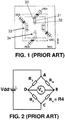
- US 4,672,411 discloses a pressure sensor (shown in FIG. 1 ) having a diaphragm formed in a semiconductor body, the diaphragm having a pair of pressure sensing semiconductor strips in a major surface thereof (vertical piezo-resistive strips 30, 31 in FIG. 1 ). Each of the strips 30, 31 is connected at one end to the other one by a semiconductor region (triangular region 32 in FIG. 1 ).
- the semiconductor region 32 is formed in a direction of small piezo-resistive coefficients, while the strips 30, 31 are formed in a direction of large piezo-resistive coefficients.
- the semiconductor region 32 (triangle) has a smaller sheet resistance than the resistance of the strips 30, 31.
- electrode lead-out regions are provided at the other ends of the strips 30, 31, which regions have low resistance, extend in a direction of small piezo-resistive coefficients, and extend beyond the edge of the diaphragm so the electrodes contact the semiconductor body outside the diaphragm.
- the resistive strips 30, 31 are connected in a Wheatstone bridge. Deformation of the diaphragm causes the diffused resistor layers (i.e. the piezo-resistive strips) to expand or shrink so as to change their resistances.
- the pressure sensor senses a pressure change by electrically detecting the change of the resistances.
- this pressure sensor is not very accurate in all circumstances, e.g. in case of temperature fluctuations, and in case of residual package-stress.
- a pressure sensor with a good accuracy, in particular in case of a non-uniform temperature (e.g. temperature gradient) of the semiconductor substrate and/or in case of packaging-stress and/or in case of a non-uniform electric field, or combinations thereof.
- a non-uniform temperature e.g. temperature gradient
- the present invention provides a semiconductor pressure sensor for determining an external pressure exerted on the sensor, comprising: a membrane as part of a semiconductor substrate for being deformed due to the external pressure, having a membrane edge and a membrane thickness; a first resistor pair located on or adjacent to a first side portion of the membrane, the first resistor pair comprising a first resistor connected between a first bias node and a first output node, and a second resistor connected between said first bias node and a second output node different from the first output node, the resistance of the second resistor being equal to that of the first resistor; a first current source connected or connectable to the first output node and adapted for causing a first predefined current to flow through the first resistor so that the first output node assumes a first output voltage; a second current source connected or connectable to the second output node and adapted for causing a second predefined current to flow through the second resistor so that the second output node assumes a second output voltage, wherein
- each output node is connected to a current source in order to obtain an output voltage between the nodes which is proportional to the external pressure.
- first resistor and the second resistor are located on the same side (e.g. edge of a square membrane), because by doing so, the distance between the resistors is small, and thus the temperature of both resistors is substantially the same. Since the resistance of the first and second resistor is equal, and since both resistors are made of the same material, the resistance of both resistors will vary with temperature, but in the same way (e.g. both increase with 5%). This will cause both output voltages to decrease with an equal amount, but will not influence the difference between them. In other words, this circuit is substantially insensitive to temperature variations (over time), and to temperature gradient over the membrane.
- the pressure sensor according to the present invention has a higher sensitivity and an improved linearity over (at least some) prior art pressure sensors.
- the layout of the first and the layout of the second resistive strips are matched.
- the semiconductor pressure sensor further comprises: a first readout circuit comprising a first differential amplifier for converting the first differential voltage signal into a first pressure signal indicative of the pressure to be measured.
- the first and the second piezo-resistive strips are formed as p doped regions within an n-well; and the biasing node is electrically connected to the n-well.
- the biasing voltage (preferably the supply voltage of the chip), is applied to the n-well and also to one end of the resistor, because this will cause a minimum (average) thickness of the depletion layer between the (p-doped) resistor and the (n-doped) n-well, allowing a higher circuit bandwidth.
- the semiconductor pressure sensor further comprises: a second resistor pair located on or adjacent to a second side portion of the membrane, wherein the second side portion is located substantially or precisely at 90° angular distance from the first side portion as measured from a center of the membrane; the second resistor pair comprising a third resistor connected in parallel with the second resistor between said first bias node and said second output node, and a fourth resistor connected in parallel with the first resistor between said first bias node and said first output node; the third resistor comprising one or more elongated piezo-resistive strips arranged in the first direction, the fourth resistor comprising one or more elongated piezo-resistive strips arranged in the second direction.
- first and fourth resistor in parallel to the first current source, and to arrange them in the manner described, because by doing so, they behave similarly to radial stress (e.g. both increase), but oppositely to uniform stress.
- the voltage created by the first current flowing through their parallel-connection has a high sensitivity to radial stress (e.g. caused by external pressure), and a reduced sensitivity to uniform stress (e.g. caused by package stress).
- the third and fourth resistor By locating the third and fourth resistor closely together (on a second side of the membrane), they will both have a similar temperature behavior (e.g. both increase or both decrease with temperature). Since R1 and R2 behave identically with temperature T1 (at a first side of the membrane), and R3 and R4 behave identically with temperature T2 (at a second side of the membrane), the parallel connection of R1 with R2 on the one hand, and R3 and R4 on the other hand, will behave almost identically with temperature variations (in first order), while being (relatively) insensitive to a temperature gradient over the membrane.
- this embodiment has the same advantages as mentioned above (high sensitivity, good linearity, low temperature influence), but in addition has a low sensitivity to uniform stress (e.g. package stress).
- the semiconductor pressure sensor further comprises:- a third resistor pair arranged at the first side portion of the membrane but outside of the membrane, the third resistor pair comprising a fifth resistor connected between said first bias node and a third output node, and a sixth resistor connected between said first bias node and a fourth output node different from the third output node; a third current source connected to the third output node and adapted for causing a third predefined current to flow through the fifth resistor so that the third output node provides a third output voltage; a fourth current source connected to the fourth output node and adapted for causing a fourth predefined current to flow through the sixth resistor so that the fourth output node provides a fourth output voltage, wherein the third and fourth predefined current is substantially equal to the first predefined current; the fifth resistor comprising one or more elongated piezo-resistive strips arranged in the first direction, and the sixth resistor comprising one or more elongated piezo-resistive strips arranged in the second
- these strips are only sensitive to (radial) package stress, but not to deformation of the membrane due to the external pressure, in contrast to the first and second resistor pairs, being mainly located on the membrane, within a distance of at most 3 times ( ⁇ 3x) the membrane thickness, which are sensitive to both (radial) package stress and the external pressure to be measured.
- the second differential voltage signal can be read by a second readout-circuit (e.g. comprising a differential amplifier, ADC, etc), and may be used by a processing unit for display, or for compensating the first differential voltage signal against package stress, e.g. by subtracting the second differential signal from the first differential signal. In this way, the package stress can be largely compensated for, or the influence thereof can at least be reduced in the final stress measurement value.
- a second readout-circuit e.g. comprising a differential amplifier, ADC, etc
- a semiconductor pressure sensor is provided with a reduced sensitivity to common mode temperature, e.g. ambient temperature (by using differential signaling), and to temperature gradients (by arranging the resistors “closely together” as pairs), and to common mode package stress (by using the third and fourth resistor and third and fourth current source, outside of the membrane), and having an increased sensitivity and improved linearity (by using current source rather than voltage source), and having a low or reduced sensitivity to temperature gradient (by using a parallel connection of resistors located at different locations), and having a reduced sensitivity to uniform stress (by locating the piezo-strips of the four resistors at 90° angular position on the membrane and by orienting the piezo-strips of the four resistors in parallel or at 90° as recited in the claim).
- common mode temperature e.g. ambient temperature (by using differential signaling), and to temperature gradients (by arranging the resistors "closely together” as pairs), and to common mode package stress (by using the third and fourth resistor
- the semiconductor pressure sensor further comprises: a multiplexer for selectively applying the first differential voltage signal and the second differential voltage signal to the first differential amplifier; and/or a second readout circuit comprising a second differential amplifier for converting the second differential voltage signal into a second pressure signal indicative of the package stress.
- each of the resistors comprises at least two or at least three piezo-resistive strips connected in series.
- the resistance value can be increased without having to decrease the doping level. This is especially advantageous when dimensions of the chip become smaller due to technology scaling.
- the piezo-resistive strips of each individual resistor are oriented in parallel.
- each of the resistors comprises an equal number of elongated piezo-resistive strips, and the dimensions of all piezo-strips is identical.
- the layout of the piezo-resistive strips, and also the interconnections between the strips belonging to a single resistor is identical (apart from rotating, shifting, mirroring), so that the resistors are better "matched".
- This offers the advantage that the resistance of the first, second, etc. resistors is equal within the tolerance margin of the process (e.g. within +/- 0.5%).
- a layout of each resistor pair further comprises a first and second leadout region for electrical interconnection to the outer nodes, and a third leadout region for electrical interconnection to the common biasing node, whereby the third leadout region is located between the first and second leadout region.
- the substrate is a CMOS wafer; and the membrane is located in the (100) plane, and at least one of the piezo-resistive elements is oriented in the ⁇ 110> direction.
- this direction is a direction of maximum piezo-resistive effect.
- a sensor having an improved, e.g. maximum sensitivity can be obtained.
- the membrane has a square or circular shape.
- the membrane has a square shape, it is advantageous to orient the sides of the square in crystallographic directions of maximum and minimum piezo-sensitivity.
- first and second resistor close to the middle of one of the sides of the square membrane.
- the deformation is larger in the middle of the sides than near the corners, and larger on the sides than in the center of the membrane, thus by providing the resistors substantially in the middle of the sides, the sensitivity of the pressure sensor is increased, e.g. maximized.
- the present invention provides a semiconductor device comprising a semiconductor pressure sensor according to the first aspect.
- the present invention provides a method of determining an external pressure exerted on a semiconductor substrate, the semiconductor substrate comprising: a membrane arranged for being deformed due to the external pressure, and having a membrane edge and a membrane thickness; a first resistor pair located on or adjacent to a first side portion of the membrane, the first resistor pair comprising a first resistor connected between a first bias node and a first output node, and a second resistor connected between said first bias node and a second output node different from the first output node, the resistance of the second resistor being equal to that of the first resistor; the first resistor comprising one or more first elongated piezo-resistive strips arranged in a first direction for measuring deformation of the membrane due to the external pressure to be measured, the second resistor comprising one or more second elongated piezo-resistive strips arranged in a second direction for measuring deformation of the membrane due to the external pressure to be measured, wherein the second direction is substantially perpen
- the method is performed using a substrate that further comprising a second resistor pair arranged as described above.
- the method is performed using a substrate that further comprises a third and a fourth resistor pair as described above, and the method further comprising the step of: applying a third predefined current to said parallel connection of the fifth resistor and the eighth resistor using a third current source; and applying a fourth predefined current to said parallel connection of the sixth resistor and the seventh resistor using a fourth current source; and measuring a second differential voltage signal over the third and fourth output node; and correcting a value corresponding to the first differential voltage signal with a value corresponding to the second differential voltage signal.
- FIG. 9 and FIG. 10 are drawn to scale.
- the terms "diaphragm” and “membrane” are used as synonyms for indicating a region of a semiconductor substrate with a reduced thickness as compared to the surrounding substrate material (also referred to as “bulk”), adapted to mechanically deform when an external pressure (to be measured) is applied thereto.
- thickness of the membrane has its usual meaning, as can be measured in a direction perpendicular to the substrate surface.
- current source or "current sink” has its usual meaning.
- An ideal current source is an electronic circuit that delivers or absorbs an electric current which is independent of the voltage across it.
- the internal resistance of an ideal current source is infinite.
- the current source has an internal resistance of at least five times the resistance of the resistor connected thereto.
- differential voltage has its usual meaning. It means the voltage difference between two nodes, as opposed to a single-ended voltage signal of a single node (implicitly measured relative to ground voltage).
- resistance is meant “electrical resistance”, unless explicitly mentioned otherwise.
- exital pressure is meant e.g. air pressure or gas pressure or fluid pressure of the environment wherein the pressure sensor is located, in contrast to “internal pressure” e.g. caused by the packaging of the semiconductor sensor.
- the membrane edges of embodiments of the present invention are preferably realized in such a way that maximum stress caused by the applied pressure is reached in at least two areas perpendicular to the membrane edge and where the membrane edge is oriented in the ⁇ 110> direction.
- Anisotropic etching of square membranes in silicon is often used as it creates four of such areas at the middle of the membrane edges due to the anisotropic etch stop on ⁇ 111> planes.
- round membranes would also result in four of such areas and oval membranes in two of such areas on the shorter diameter.
- the stress sensitivity of piezo-resistors also depends on the crystal orientation and the p doped resistors have a maximum change in resistance along the ⁇ 110> directions, and a minimum change in resistance along the ⁇ 100> directions, at 45° from the ⁇ 110> directions.
- Metal connections cause stress in the silicon and due to creep this stress can also change over time. Therefore a highly doped p doped path is realized between the metal and the piezo-resistive strips. By placing these highly p doped paths in the ⁇ 100> directions at 45 degrees of the ⁇ 110> directions one assures that stress from the metal lines does not change the resistance of these strips.
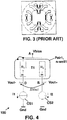
- Wheatstone-bridge circuits with four resistors R1, R2, R3, R4 arranged as shown in FIG. 2 are well known in the art. Such circuits are very well suited for determining an unknown resistor value Rx, when three other resistor values R1, R2 and R3 are known, or for detecting/measuring small resistance changes when all four resistor values are known.
- the bridge of FIG. 2 has four resistors R1, R2, R3 and R4 (or Rx).
- Vdd and Gnd are applied to the nodes A and C, respectively, a first current will flow from A to C through the first branch formed by R1 in series with R2, and a second current will flow through the second branch formed by R3 in series with R4.
- the voltages Vd and Vb can be read-out by a circuit having a large input impedance (in order not to draw additional current).
- the nodes D and B are connected to a differential amplifier which amplifies the differential voltage Vout. The amplified signal can then be used for further processing.
- An ideal pressure sensor has a high sensitivity (large output signal for even a small pressure), has zero offset, has a perfect linear behaviour (output voltage exactly proportional to the applied pressure), and is insensitive to temperature variations and package stress. Furthermore it is insensitive to electric fields perpendicular to the surface.
- Zero offset means that the voltage output over the nodes D and B should be exactly zero when no pressure is applied to the membrane 2, and ideally this value should remain exactly zero irrespective of the sensor temperature in the absence of external pressure. In practice, however, the output voltage value Vg corresponding to zero-pressure, is not exactly zero, and needs to be compensated for, in order to achieve an accurate pressure measurement value.
- This non-zero value is called “zero-offset”, i.e. the voltage offset value between nodes D and B when no external pressure is exerted on (or applied to) the sensor membrane.
- zero-offset i.e. the voltage offset value between nodes D and B when no external pressure is exerted on (or applied to) the sensor membrane.
- There may be various causes of such zero-offset e.g. mismatch between the various resistance values due to imperfections of the semiconductor processing, residual stresses in the membrane due to packaging of the semiconductor (e.g.
- FIG. 3 shows a prior art pressure sensor disclosed by Honeywell in EP0083496 . It is noted that in the illustration in the present document black lines are added to FIG. 3 , to clearly indicate the position and orientation of the piezo-resistive strips.
- This sensor has a first bridge with resistors located on the membrane for measuring the external pressure exerted on the membrane. This first bridge has a zero-offset due to temperature variations and due to package stress. This offset - may be compensated by using the output of a second bridge, having four resistors located outside the membrane. This total double bridge sensor provides a pressure value that is compensated for package stress, however, the compensation is not perfect.
- Zero-offset compensation for example by measuring the offset (at zero external pressure) during a calibration stage, and storing the offset-values in a non-volatile memory (e.g. flash), and compensating the readout by measuring the temperature, and by subtracting the stored value, are also known in the art.
- a non-volatile memory e.g. flash
- FIG. 4 shows a schematic block-diagram and FIG. 5 shows an example of a partial layout of a first embodiment of a semiconductor pressure sensor 100 according to the present invention.
- the length of the piezo-resistive strips may be a value in the range of 6 ⁇ m to 60 ⁇ m
- the width of the membrane may for example be a value in the range of 150 ⁇ m to 1500 ⁇ m, but the ratio of the length of the strip and the width of the membrane need not be equal to 1/10, but may for example be a value in the range of 1/50 to 1/10 , for example be a value in the range of 0.5% to 30%, or be a value in the range of 1% to 20%, or a value in the range of 2% to 10%, for example about 4% or about 8% or about 12% or about 15%.
- the pressure sensor 100 comprises a membrane 2 as part of a semiconductor substrate having a shape and dimensions for allowing the membrane 2 to be mechanically deformed due to an external pressure.
- the membrane 2 has a membrane edge 21 and a membrane thickness.
- the membrane 2 advantageously has a square or circular shape, but other shapes may also be used, for example: rectangular, polygonal, hexagonal, octagonal, or any other suitable shape.
- the pressure sensor 100 further comprises a (first) resistor pair P1 located on or adjacent to a first side portion S1 of the membrane 2.
- the (first) resistor pair P1 comprises a first resistor R1 connected between a first bias node A and a first output node D, and a second resistor R2 connected between said (same) first bias node A and a second output node B, different from the first output node D.
- a biasing voltage e.g. the chip supply voltage VDD is applied to the biasing node A.
- VDD chip supply voltage
- this low-ohmic contact is also used to maintain the potential of the n-type silicon around the p-type piezoresistors the same or higher than the local potential of the p-type resistors to form an isolating depletion layer.
- the (electrical) resistance of the second resistor R2 is substantially equal, e.g. equal to that of the first resistor R1 (in the absence of external pressure), within a very small tolerance margin (e.g. less than 1%, preferably less than 0.25%), which is achieved inter alia by matching the layout of the resistors, and in some embodiments, by placing the two resistors in a single N-well.
- the pressure sensor 100 further comprises a first current source CS1 connected to the first output node D and adapted for causing a first predefined current I1 to flow through the first resistor R1 so that the first output node D assumes a first output voltage Vout-, and a second current source CS2 connected to the second output node B, and adapted for causing a second predefined current I2 to flow through the second resistor R2 so that the second output node B assumes a second output voltage Vout+.
- Current sources adapted for providing a current which is quite independent of temperature are well known in the art of semiconductor devices, and hence need not be described in detail here.
- the current sources CS1 and CS2 are "matched", and provide a predefined current I1 and I2, which are identical within a tolerance margin less than 1.0%, preferably less than 0.5% or even less than 0.25%.
- the current source CS1 and CS2 have substantially the same quality of matching as the resistors R1, R2 or better by using switching techniques.
- the current sources CS1, CS2 have a "large" output impedance, e.g. at least 5 times the resistance R1, R2, for example at least 10 times or at least 20 times.
- the first resistor R1 comprises one or more, for example two or three first elongated piezo-resistive strips 8 arranged in a first direction X for measuring deformation of the membrane 2 due to the external pressure to be measured.
- the second resistor R2 comprise one or more, for example two or three second elongated piezo-resistive strips 9 arranged in a second direction Y, substantially orthogonal to the first direction X, for measuring deformation of the membrane 2 due to said external pressure.
- the layout of the first and second resistive strips 8, 9 are matched, meaning that the strips have an identical layout (apart from translation, rotation, and mirroring.
- R1 and R2 are arranged such that, if R1 increases due to external pressure, then R2 decreases, or vice versa.
- the first resistor R1 and the second resistor R2 are deliberately located on the same side (more specifically near the middle of a first side S1 of a square membrane), rather than being arranged on different sides of the membrane 2.
- the distance between the resistors is "small", and thus the temperature T1, T2 of the resistors R1, R2 is substantially the same (T1 ⁇ T2). Since the resistance of the first and second resistor is equal, and since both resistors are made of the same material, the resistance of both resistors will vary with temperature in the same way (e.g. both increase with 5% when temperature increases).
- the first and second output voltage Vout-, Vout+ form a first differential voltage signal ⁇ Vout indicative of the external pressure to be measured.
- the first differential voltage signal ⁇ Vout is substantially proportional to the external pressure applied to the pressure sensor, because the circuit provides two output voltages which vary linearly with change of the resistance R1, R2, which in turn vary linearly with deformation of the membrane, which is turn varies linearly with the amount of external pressure applied to the membrane 2.
- This non-linearity is avoided in the circuits proposed by the present invention by using the current sources CS1, CS2. It is a major advantage of the present invention that it provides an output signal ⁇ Vout with an improved linearity.
- FIG. 9 shows the layout pattern of FIG. 5 in more detail (and mirrored).
- the "lead-out regions" 6, as well as “corner parts” 3 interconnecting the piezo-resistive strips 8, 9 are made of a heavily-doped layer of the first dopant type, for instance a heavily-doped p+ type diffused layer. They have a relatively low electrical resistance, and extend in a direction of relatively small piezo-resistive coefficients (in the example shown, preferably at angles of +/- 45° with respect to the first and second direction Y, X).
- the lead-out regions 6 extend beyond the edge 21 of the membrane 2, and are in ohmic contact with conductor electrodes, e.g. metal electrodes 4, located on the bulk, outside of the membrane 2.
- Such metal electrodes 4 may e.g. comprise aluminum.
- the diffused layers of the first dopant type, e.g. p type diffused layers, 8, 9 constituting the pressure sensing elements have a relatively large, e.g. the maximum, piezo-resistive coefficient, their electrical resistance is varied greatly by a strain which develops due to the deformation of the semiconductor, e.g. silicon, membrane 2. That is, these pressure sensing elements are very sensitive to a pressure or the like.
- the diffused layers are heavily doped with dopants of the first dopant type, e.g. heavily-doped p+ diffused layers, the interconnections 3 and 6 are arranged in orientations of relatively small, e.g.
- the influence which is exerted on the deformation of the semiconductor, e.g. silicon, membrane by the residual stress developing in the vicinity of the contact portion, and any hysteresis due to temperature changes, can be reduced, e.g. minimized.
- a particular advantage of the layout shown in FIG. 9 is that the lead-out portion 6b of the (common) node A is routed between the lead-out portions 6a, 6b of the output nodes D, B. This offers the advantage that the routing passes only over a minimal distance (or no distance at all) over the membrane 2.
- the resistors R1 and R2 are of p type semiconductor material, embedded in an N-well structure.
- the N-well is electrically connected to the biasing node A (as explicitly shown in FIG. 4 and FIG. 6 ).
- the entire membrane is made of n-type material, acting as N-well. In this case the membrane establishes the depletion layer for all resistors. By doing so, the thickness of the depletion layer between the p-type resistor material and the N-well is reduced to a minimum and kept the same for both resistors, which allows a faster readout (higher bandwidth). Indeed, in the embodiment of FIG.
- the voltage difference between the resistor R1, R2 and the n-well is (Vbias - I x R) at one end of the resistor, and is Vbias at the other end of the resistor, thus on average: Vbias - (I x R)/2, which is typically somewhat higher than in the case of FIG. 4 .
- the depletion layer between the resistors and the N-well will (typically) have a larger thickness T in the embodiment of FIG. 6 as compared to that of FIG. 4 , which is disadvantageous for fast readout.
- the circuit of FIG. 6 needs four contacts as preferably the n-well is connected to a low ohmic voltage node with a voltage which is equal to or higher than the voltage on the nodes D and B.
- the depletion layer forms a capacitive load and by connecting it to one of the outputs and not separately the matching of the resistors is compromised as the resistor connected to n-well with have a much higher capacitance than the resistor that is not connected to the well.
- the configuration of FIG. 6 will need four bondpads whereas the configuration of FIG. 4 needs only three bondpads. In other words: if the resistor-layout structure of FIG. 9 is to be used in the circuit of FIG.
- either the N-well can be connected to the bias-voltage (e.g. via an additional bondpad, in case the membrane-substrate and the substrate with the current sources is not the same), or alternatively, the N-well can be connected to one of the output nodes, but this has the disadvantage of creating an asymmetric capacitive impedance for the two resistors R1, R2.
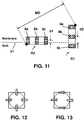
- FIG. 10 shows another example of a layout pattern as can be used in embodiments of the pressure sensor 100, 200 described above.
- each resistor R1, R2 contains three piezo-resistive strips 8, 9 (indicated in dark gray) arranged in "close vicinity" of the membrane edge 21. What is meant with “close” and “near” will be quantified when describing FIG. 11 .
- the piezo-resistive strips 8, 9 of each particular resistor are parallel to each other, but the piezo-resistive strips of the different resistors of the pair are oriented orthogonally with respect to each other.
- FIG. 11 shows an enlarged view of the piezo-resistive strips 8, 9 of FIG. 10 .
- the piezo-resistive strips 8, 9 are located "closely together near the membrane edge".
- a maximum distance MD is defined between a point of the first resistor strips 8 (of the first resistor R1) and a point of the second resistor strips 9 (of the second resistor R2), where said points are indicated by black dots for illustrative purposes.
- the ratio of said maximum distance MD and a dimension of the membrane 2 is less than 50%, preferably less than 40%, preferably less than 35%, preferably less than 30%, preferably less than 25%, preferably less than 20%, preferably less than 15%, such as e.g. about 10%.
- the ratio would be calculated as the length of said maximum distance MD over the diameter of the circle.
- the ratio would be calculated as the maximum distance MD over the larger of the two axes of the ellipse.
- the ratio would be calculated as the length of said diagonal MD over the distance between opposite sides of the octagonal, etc.
- the resistors R1, R2 are preferably also located "about in the middle" of the side S1 of the membrane 2, because for a square membrane shape, maximum tensile stress is created in the middle of each side.
- “about in the middle of a side” is meant within an imaginary circle having its centre in the middle of the side, and having a diameter less than 50% of the above mentioned “dimension of the membrane” (e.g. the width of a square, the diameter of a circle, etc.), preferably less than 40%, more preferably less than 30%, even more preferably less than 20%.
- the membrane does not have "sides", but the same definition can be used considering the tangential square (as illustrated). Also for round membranes the strips have to be aligned in the ⁇ 110> directions in order to have maximum piezoresistive sensitivity.
- the position of the piezo-resistive strips 8, 9 with respect to the membrane edge 21 may be chosen to create a maximum of resistance change of the three strips together (e.g. ⁇ R1) when a pressure is applied.
- the optimal distance "d1" in terms of maximum sensitivity w.r.t. pressure can be determined, e.g. calculated or simulated or determined in any other way, e.g. via design variation.
- an optimal distance "d2" in terms of maximum sensitivity w.r.t. pressure can be determined.
- the value of "d2" can be determined independent of the value of "d1”, but is dependent on the membrane size and membrane thickness T.
- Finite element modeling may be used to determine these "optimal" distances d1, d2.
- the invention will also work with sub-optimal positions. Simulations have shown that such an optimal position may e.g.
- the resistors R1 and R2 of the first pair are arranged "close” together (relative to the size of the membrane 2), and it can therefore be assumed (or approximated) that the temperatures of the piezo-resistive strips of R1 and R2 are substantially the same, say T1.
- T1 the temperatures of the piezo-resistive strips of R1 and R2 are substantially the same, say T1.
- between the resistors R1, R2 would also only be a fraction of the total temperature difference which may exist over the membrane 2. Hence, the sensitivity of the pressure sensor in respect of any temperature gradient over the membrane 2 is drastically reduced, and thus the accuracy of the pressure sensor is increased.
- FIG. 12 is a schematic representation of radial stress (e.g. caused by external pressure) shown at four locations of a square membrane, which stress is typically caused by a pressure (to be measured) exerted on the membrane in a direction perpendicular to the substrate. It can then be understood that, when the orientation of the piezo-resistive strips 8, 9 of R1 and R2 are orthogonal to each other, the effect of such radial pressure exerted in a direction substantially perpendicular to the plane XY of the membrane 2 (in the Z-direction), will cause the value of R1 to increase (because the length of the piezo-strips increases), and the value of R2 to decrease (because their width increases), or vice versa.
- radial stress e.g. caused by external pressure
- FIG. 13 is a schematic representation of uniform (non-radial) stress (in the example shown from left to right) at four locations of a square membrane, which uniform non-radial stress may be caused by packaging. How would the circuit of FIG. 4 react to such stress? In the case illustrated in FIG. 13 , the value of R1 would increase, and the value of R2 would decrease, hence the circuit of FIG. 4 cannot differentiate between external pressure and uniform non-radial package stress, which is a disadvantage of the first embodiment. (Of course, the corresponding zero-offset can still be reduced in other ways, e.g. by measuring the zero-offset during production, storing said value in flash, and subtracting the value during actual use of the device).
- FIG. 5 is already discussed above.
- the drawing shows an embodiment with a circular membrane, and with a square membrane in a single drawing.
- the behavior of both implementations is very similar. While the dual-resistor-layout of FIG. 9 (with two resistors, each having two piezo-resistive strips) was used in the pressure sensor 100 of FIG. 5 , it shall be clear that the layout of FIG. 10 (with two resistors, each having three piezo-resistive strips) could also have been used.
- FIG. 6 shows a schematic block-diagram of a second embodiment of a pressure sensor 200 according to the present invention. This is a variant of FIG. 4 , and was already shortly discussed above. Everything which is mentioned above for the first embodiment 100 is also applicable for this embodiment, except that the position of the resistors R1, R2 and the current sources CS1, CS2 is swapped. Indeed, in FIG. 4 the current sources are connected with one end to ground whereas in FIG. 6 the current sources are connected with one end to the bias node A. Further, in FIG. 4 the resistors R1 and R2 are connected with one node to the bias node A whereas in FIG. 6 the resistors are connected with one node to ground.
- the behavior and performance of the second embodiment 200 is very similar to that of the first embodiment 100, except for the capacitance of the resistors R1, R2, which is relevant for AC measurements and transient behavior.
- the thickness of the depletion layer between the resistors R1, R2 and the N-well in FIG. 6 is typically larger than that of FIG. 4 , hence the embodiment of FIG. 6 may have a reduced bandwidth.
- the second embodiment offers the same advantages of high/improved sensitivity, good/improved linearity, insensitivity to temperature variations and temperature gradient, listed in TABLE 1. By the addition of a separate bias contact for the N-well the resistors R1, R2 can also be matched for the capacitance of the depletion layer.
- FIG. 7 shows a schematic block-diagram of a third embodiment of a pressure sensor 300 according to the present invention
- FIG. 8 shows an example of a possible layout of part thereof.
- the pressure sensor 300 has all the components of the pressure sensor 100 of the first embodiment, and therefore, everything which is mentioned above for the first embodiment, is also applicable for this embodiment, unless specifically mentioned otherwise.
- this embodiment further comprises: a second resistor pair P2 located on or adjacent to a second side portion S2 of the membrane 2.
- the second side portion S2 is located at 90° angular distance from the first side portion S1 as measured from a center of the membrane 2.
- the second resistor pair P2 comprises a third resistor R3 electrically connected in parallel with the second resistor R2 between said (first) bias node A and said second output node B, and a fourth resistor R4 connected in parallel with the first resistor R1 between said (first) bias node A and said first output node D.
- the third resistor R3 comprises one or more, e.g. two or three third elongated piezo-resistive strips 10 arranged in the first direction X.
- the fourth resistor R4 comprises one or more second elongated piezo-resistive strips 11 arranged in the second direction Y.
- R1, R2, R3, R4 is a graphical indication meaning that if the resistance value of R1 increases due to the external pressure, then the value of R4 also increases, but the value of R2 and R3 decrease.
- Comparison of Table 2 and Table 1 shows that the main advantage of a pressure sensor 300 according to the third embodiment is that it has the additional advantage of being relatively insensitive to uniform (non-radial) stress, e.g. package stress.
- FIG. 8 will not be described in detail, because it is very similar to FIG. 5 .
- the reader will understand that, even though the resistors R1,R2,R3,R4 are shown with only piezo-resistive strips (using the layout of FIG. 9 ), it is of course also possible to a resistor-layout with three piezo-strips (using the layout of FIG. 10 ). It is preferably if the same layout pattern (apart from shifting, rotating and mirroring) is used for the first resistor pair P1 and for the second resistor pair P2, but that is not absolutely required, and the invention will also work if for example the first resistor pair P1 would use the layout of FIG. 9 , and the second resistor pair P2 would use the layout of FIG.
- FIG. 9 is already described above. However, when used in the second embodiment 200 ( FIG. 6 ), a modification needs to be made, because Vbias would be actually Ground, and the N-well would be connected to Vdd, not to ground. Thus, the "n-contact" would have to be provided via a fourth contact, rather than via the contact of Vbias. The same applies for FIG . 10 , when used in the second embodiment 200.
- FIG. 11 to FIG. 13 were already discussed above.
- FIG. 14 illustrates a fourth embodiment of a pressure sensor 400 according to the present invention.
- a pressure sensor 400 according to the fourth embodiment has all the features of a pressure sensor according to the third embodiment.
- the circuit shown in FIG. 7 will be referred to as "first sub-circuit”.
- a pressure sensor according to the fourth embodiment would then have also a "second sub-circuit", electrically identical to the first sub-circuit shown in FIG. 7 , but comprising a third and fourth resistor pair P3, P4 (instead of P1, P2) and with a third and fourth current source CS3, CS4 (instead of CS1, CS2).
- the second sub-circuit comprising P3, P4, CS3, CS4 is preferably biased by the same bias voltage Vbias and ground Gnd as the first sub-circuit, although that is not absolutely required.
- the second sub-circuit provides a second differential output signal ⁇ Vref.
- the third pair P3 comprises two resistors R5, R6 (corresponding to R1 and R2 of the first sub-circuit) and the fourth pair P4 comprises two resistors R7, R8 (corresponding to R3 and R4 of the first sub-circuit).
- the resistors R5, R6, R7, R8 are located adjacent to and substantially in the middle of the first and second side S1, S2 of the membrane 2, outside the membrane 2, on the bulk material. They are not intended for measuring deflections of the membrane 2, but for measuring only (radial) strain due to packaging.
- the piezo-resistive strips of R5 and R6 are located "closely together" relative to the membrane size (using the same formula MD/W), and hence the temperature of the fifth and sixth resistors R5, R6 can be considered to be substantially the same, say T5. Likewise the temperature of the seventh and eighth resistor R7, R8 can be considered substantially the same.
- the second sub-circuit is substantially insensitive, e.g. insensitive to a temperature gradient, which is a major advantage over the prior art, when using the output ⁇ Vref of the second sub-circuit comprising P3, P4 to correct the output ⁇ Vout of the first sub-circuit comprising P1, P2.
- the third resistor pair P3 is located relatively "close” to the first resistor pair P1
- the fourth resistor pair P4 is located relatively “close” to the second resistor pair P2, such that the pressure sensed by the third resistor pair P3 due to the packaging is substantially the same as the pressure exerted by the package on the first resistor pair P1, and the pressure sensed by the fourth resistor pair P4 due to the packaging is substantially the same as the pressure exerted by the package on the second resistor pair P2.
- the value measured by the first (inner) sub-circuit is indicative for the external pressure and package stress
- the value measured by the second sub-circuit is indicative for the package stress only. If an identical layout is chosen for the resistors R1-R4 and for R5-R8 of the first and the second sub-circuit, and if the same bias voltage Vbias is chosen for the first and second sub-circuit (in FIG. 14 they are hard-wired), the value of the second sub-circuit can be subtracted from the value of the first sub-circuit to compensate for package stress, in ways known in the art (for example by a digital controller, after ADC).
- the value of the second sub-circuit would be proportional to the package stress, and a predefined fraction of the value ⁇ Vref can be subtracted in another manner (e.g. in an analog manner) from the output ⁇ Vout of the first sub-circuit to compensate the zero-offset against package stress.
- the main reason for locating the third pair P3 close to the first pair P1 is to match the package stress as good as possible. Since the resistors R1 to R4 are located on the membrane 2, (or more correctly stated: a major portion of R1 and R4 is located on the membrane) they are sensitive to pressure exerted on the membrane 2 as well as to pressure exerted by the package.
- the resistors R5 to R8 are located "sufficiently far" outside the membrane 2, e.g. at least 4.0 times ( ⁇ 4x) the membrane thickness T away from the membrane edge 21, or at least 6.0 times, or at least 10.0 times, they are only sensitive to the pressure exerted by the package.
- the second sub-circuit comprising the resistors R5 to R8 can be used to determine the radial pressure exerted by the package on the substrate, which radial pressure can be used to compensate the pressure value obtained from the first sub-circuit, using known methods.
- the third and fourth resistor pair P3, P4 may e.g. be located at a distance equal to about 4.0 times (4x) to about 10.0 times (10x) the membrane thickness T.
- a pressure sensor 400 according to the third embodiment has all advantages of a pressure sensor according to the third embodiment (listed in TABLE 2), and in addition has an improved accuracy because it has an improved compensation of (radial) package stress.
- the present invention also relates to a semiconductor device comprising a pressure sensor 100, 200, 300, 400 as described above.
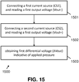
- the present invention relates to a method 1500 of determining an external pressure exerted on a semiconductor substrate, where the semiconductor substrate comprises a membrane 2 and a resistor structure having one resistor pair P1 arranged as described above (first embodiment or second embodiment and shown in FIG. 4 to FIG. 6 ), whereby the method comprises the steps of: applying 1501 a first predefined current I1 to said first resistor R1 by connecting a first current source CS1; applying 1502 a second predefined current I2 to said second resistor R2 by connecting a second current source CS2; obtaining 1503 a first differential voltage signal ⁇ Vout over the first and second output node B, D.
- the current sources CS1 and CS2 may, or may not be part of the same substrate as the one where the membrane is located, but could be located on a second substrate (not shown), connectable to the first substrate via for example three or four bondpads.
- the present invention also relates to a method of determining an external pressure exerted on a semiconductor substrate having a membrane 2 and two resistor pairs P1, P2 arranged as described above (third embodiment, and shown in FIG. 7 and FIG. 8 ).
- This method comprises the steps of: applying a first predefined current I1 to said parallel connection of the first resistor R1 and fourth resistor R4 using a first current source CS1; applying a second predefined current I2 to said parallel connection of the second resistor R2 and third resistor R3 using a second current source CS2; and measuring a first differential voltage signal About over the first and second output node B, D.
- the present invention also relates to a method of determining an external pressure exerted on a semiconductor substrate having a membrane 2 and two resistor pairs P1, P2 arranged as described above (fourth embodiment, and shown in FIG. 14 ).
- This method comprises the steps of: applying a first predefined current I1 to said parallel connection of the first resistor R1 and fourth resistor R4 using a first current source CS1; applying a second predefined current I2 to said parallel connection of the second resistor R2 and third resistor R3 using a second current source CS2; and measuring a first differential voltage signal ⁇ Vout over the first and second output node B, D; and applying a third predefined current I3 to said parallel connection of R5 and R8 using a third current source CS3; applying a fourth predefined current I4 to said parallel connection of R6 and R7 using a fourth current source CS4; and measuring a second differential voltage signal ⁇ Vref over the third and fourth output node B2, D2; and correcting a value corresponding
Landscapes
- Physics & Mathematics (AREA)
- General Physics & Mathematics (AREA)
- Measuring Fluid Pressure (AREA)
- Pressure Sensors (AREA)
Claims (15)
- Halbleiterdrucksensor (100, 200, 300, 400) zur Bestimmung eines auf den Sensor ausgeübten externen Drucks, umfassend:- eine Membran (2) als Teil eines Halbleitersubstrats, um durch den externen Druck verformt zu werden, die einen Membranrand (21) und eine Membrandicke (T) aufweist;- ein erstes Widerstandspaar (P1), das sich auf oder angrenzend an einen ersten Seitenabschnitt (S1) der Membran (2) befindet, wobei das erste Widerstandspaar (P1) einen ersten Widerstand (R1) umfasst, der zwischen einem ersten Vorspannungsknoten (A) und einem ersten Ausgangsknoten (D) angeschlossen ist, und einen zweiten Widerstand (R2), der zwischen dem besagten ersten Vorspannungsknoten (A) und einem zweiten Ausgangsknoten (B) angeschlossen ist, der sich vom ersten Ausgangsknoten (D) unterscheidet, wobei der Widerstand des zweiten Widerstands (R2) gleich jenem des ersten Widerstands (R1) ist;- eine erste Stromquelle (CS1), die an den ersten Ausgangsknoten (D) angeschlossen ist oder angeschlossen werden kann, und ausgeführt ist, um einen ersten vordefinierten Strom (I1) dazu zu bringen, durch den ersten Widerstand (R1) zu fließen, sodass der erste Ausgangsknoten (D) eine erste Ausgangsspannung (Vout-) übernimmt;- eine zweite Stromquelle (CS2), die an den zweiten Ausgangsknoten (B) angeschlossen ist oder angeschlossen werden kann, und ausgeführt ist, um einen zweiten vordefinierten Strom (12) dazu zu bringen, durch den zweiten Widerstand (R2) zu fließen, sodass der zweite Ausgangsknoten (B) eine zweite Ausgangsspannung (Vout+) übernimmt, wobei der zweite vordefinierte Strom (12) im Wesentlichen gleich dem ersten vordefinierten Strom (I1) ist;- wobei der erste Widerstand (R1) einen oder mehrere erste längliche piezoresistive Streifen (8) umfasst, die in einer ersten Richtung (X) angeordnet sind, um die Verformung der Membran (2) aufgrund des zu messenden externen Drucks zu messen, wobei der zweite Widerstand (R2) einen oder mehrere zweite längliche piezoresistive Streifen (9) umfasst, die in einer zweiten Richtung (Y) angeordnet sind, um die Verformung der Membran (2) aufgrund des zu messenden externen Drucks zu messen, wobei die zweite Richtung (Y) im Wesentlichen senkrecht zur ersten Richtung (X) verläuft;- wobei die erste und die zweite Ausgangsspannung (Vout-, Vout+) ein erstes Differenzspannungssignal (ΔVout) bilden, das auf den zu messenden externen Druck hinweist.
- Halbleiterdrucksensor (100, 200, 300, 400) nach Anspruch 1, darüber hinaus umfassend: einen ersten Auslesekreis, einen ersten Differenzverstärker umfassend, zum Umwandeln des ersten Differenzspannungssignals (ΔVout) in ein erstes Drucksignal, das auf den zu messenden externen Druck hinweist.
- Halbleiterdrucksensor (100, 200, 300, 400) nach Anspruch 1 oder 2,- wobei der erste und der zweite piezoresistive Streifen (8, 9) als p-dotierte Regionen in einer n-Mulde gebildet werden; und- wobei der Vorspannungsknoten (A) elektrisch an die n-Mulde angeschlossen ist.
- Halbleiterdrucksensor (300, 400) nach einem der vorhergehenden Ansprüche, darüber hinaus umfassend:- ein zweites Widerstandspaar (P2), das sich auf oder angrenzend an einen zweiten Seitenabschnitt (S2) der Membran befindet, wobei sich der zweite Seitenabschnitt (S2) im Wesentlichen oder präzise, wie von einer Mitte der Membran (2) gemessen, in einem 90 ° Winkelabstand vom ersten Seitenabschnitt (S1) befindet;- wobei das zweite Widerstandspaar (P2) einen dritten Widerstand (R3) umfasst, der parallel zum zweiten Widerstand (R2) zwischen dem besagten ersten Vorspannungsknoten (A) und dem besagten zweiten Ausgangsknoten (B) angeschlossen ist, und einen vierten Widerstand (R4), der parallel zum ersten Widerstand (R1) zwischen dem besagten ersten Vorspannungsknoten (A) und dem besagten ersten Ausgangsknoten (D) angeschlossen ist;- wobei der dritte Widerstand (R3) einen oder mehrere längliche piezoresistive Streifen (10) umfasst, die in der ersten Richtung (X) angeordnet sind, wobei der vierte Widerstand (R4) einen oder mehrere längliche piezoresistive Streifen (11) umfasst, die in der zweiten Richtung (Y) angeordnet sind.
- Halbleiterdrucksensor (400) nach einem der vorhergehenden Ansprüche, darüber hinaus umfassend:- ein drittes Widerstandspaar (P3), das im ersten Seitenabschnitt (S1) der Membran (2), jedoch außerhalb der Membran (2) angeordnet ist, wobei das dritte Widerstandspaar (P3) einen fünften Widerstand (R5) umfasst, der zwischen dem besagten ersten Vorspannungsknoten (A) und einem dritten Ausgangsknoten (D2) angeschlossen ist, und einen sechsten Widerstand (R6), der zwischen dem besagten ersten Vorspannungsknoten (A) und einem vierten Ausgangsknoten (B2) angeschlossen ist, der sich vom dritten Ausgangsknoten (D2) unterscheidet;- eine dritte Stromquelle (CS3), die an den dritten Ausgangsknoten (D2) angeschlossen ist und ausgeführt ist, um einen dritten vordefinierten Strom (13) dazu zu bringen, durch den fünften Widerstand (R5) zu fließen, sodass der dritte Ausgangsknoten (D2) eine dritte Ausgangsspannung (Vref-) bereitstellt;- eine vierte Stromquelle (CS4), die an den vierten Ausgangsknoten (B2) angeschlossen ist und ausgeführt ist, um einen vierten vordefinierten Strom (14) dazu zu bringen, durch den sechsten Widerstand (R6) zu fließen, sodass der vierte Ausgangsknoten (B2) eine vierte Ausgangsspannung (Vref+) bereitstellt, wobei der dritte und vierte vordefinierte Strom (13, 14) im Wesentlichen gleich dem ersten vordefinierten Strom (I1) sind;- wobei der fünfte Widerstand (R5) einen oder mehrere längliche piezoresistive Streifen umfasst, die in der ersten Richtung (X) angeordnet sind, und der sechste Widerstand (R6) einen oder mehrere längliche piezoresistive Streifen umfasst, die in der zweiten Richtung (Y) angeordnet sind um Verpackungsbeanspruchung zu messen;- und ein viertes Widerstandspaar (P4), das im zweiten Seitenabschnitt (S2) der Membran (2), jedoch außerhalb der Membran (2) angeordnet ist, wobei das vierte Widerstandspaar (P4) einen siebten Widerstand (R7) umfasst, der parallel zum sechsten Widerstand (R6) zwischen dem besagten ersten Vorspannungsknoten (A) und dem besagten vierten Ausgangsknoten (B2) angeschlossen ist, und einen achten Widerstand (R8), der parallel zum fünften Widerstand (R5) zwischen dem besagten ersten Vorspannungsknoten (A) und dem besagten dritten Ausgangsknoten (D2) angeschlossen ist, wobei der siebte Widerstand (R7) einen oder mehrere längliche piezoresistive Streifen umfasst, die in der ersten Richtung (X) angeordnet sind, wobei der achte Widerstand (R8) einen oder mehrere längliche piezoresistive Streifen umfasst, die in der zweiten Richtung (Y) angeordnet sind;- wobei der eine oder mehrere längliche piezoresistive Streifen des fünften und sechsten und siebten und achten Widerstands (R5, R6, R7, R8) in einem Abstand vom Membranrand (21) von mindestens 4,0 Mal der Membrandicke (T) nur zum Messen der Beanspruchung angeordnet sind, die durch die Verpackung auf das Halbleitersubstrat ausgeübt wird;- wobei die dritte und vierte Ausgangsspannung (Vref-, Vref+) ein zweites Differenzspannungssignal (ΔVref) bilden, das auf die Verpackungsbeanspruchung hinweist.
- Halbleiterdrucksensor (400) nach Anspruch 5, darüber hinaus umfassend:- einen Multiplexer zur selektiven Anwendung des ersten Differenzspannungssignals (ΔVout) und des zweiten Differenzspannungssignals (ΔVref) auf den ersten Differenzverstärker; und/ oder- einen zweiten Auslesekreis, einen zweiten Differenzverstärker umfassend, zum Umwandeln des zweiten Differenzspannungssignals (ΔVref) in ein zweites Drucksignal, das auf die Verpackungsbeanspruchung hinweist.
- Halbleiterdrucksensor (100, 200, 300, 400) nach einem der vorhergehenden Ansprüche, wobei jeder der Widerstände (R1, R2; R1, R2, R3, R4; R1, R2, R3, R4, R5, R6, R7, R8) zumindest zwei oder zumindest drei piezoresistive Streifen umfasst, die in Reihe angeschlossen sind.
- Halbleiterdrucksensor (100, 200, 300, 400) nach einem der Ansprüche 1 bis 7, wobei jeder der Widerstände (R1, R2; R1, R2, R3, R4; R1, R2, R3, R4, R5, R6, R7, R8) eine gleiche Anzahl an länglichen piezoresistiven Streifen (8, 9; 8, 9, 10, 11) umfasst und wobei die Abmessungen aller piezoresistiven Streifen identisch ist.
- Halbleiterdrucksensor (100, 200, 300, 400) nach Anspruch 7 oder 8, wobei eine Gestaltung eines jeden Widerstandspaares (P1; P1, P2; P1, P2, P3, P4) darüber hinaus eine erste und zweite Durchführungsregion (6a, 6c) für die elektrische Zusammenschaltung mit den äußeren Knoten (D, B) umfasst, und eine dritte Durchführungsregion (6b) für die elektrische Zusammenschaltung mit dem gemeinsamen Knoten (A), wobei sich die dritte Durchführungsregion (6b) zwischen der ersten und zweiten Durchführungsregion befindet.
- Halbleiterdrucksensor (100, 200, 300, 400) nach einem der Ansprüche 1 bis 9,- wobei das Substrat ein CMOS Wafer ist; und- wobei sich die Membran in der (100) Ebene befindet und zumindest eines der piezoresistiven Elemente in der <110> Richtung ausgerichtet ist.
- Halbleiterdrucksensor (100, 200, 300, 400) nach Anspruch 10, wobei die Membran eine quadratische oder kreisförmige Form aufweist.
- Halbleitervorrichtung, einen Halbleiterdrucksensor (100, 200, 300, 400) nach einem der vorhergehenden Ansprüche umfassend.
- Verfahren (1500) zur Bestimmung eines auf ein Halbleitersubstrat ausgeübten externen Drucks, wobei das Halbleitersubstrat umfasst:- eine Membran (2), die angeordnet ist, um aufgrund des externen Drucks verformt zu werden, und die einen Membranrand (21) und eine Membrandicke (T) aufweist;- ein erstes Widerstandspaar (P1), das sich auf oder angrenzend an einen ersten Seitenabschnitt (S1) der Membran (2) befindet, wobei das erste Widerstandspaar (P1) einen ersten Widerstand (R1) umfasst, der zwischen einem ersten Vorspannungsknoten (A) und einem ersten Ausgangsknoten (D) angeschlossen ist, und einen zweiten Widerstand (R2), der zwischen dem besagten ersten Vorspannungsknoten (A) und einem zweiten Ausgangsknoten (B) angeschlossen ist, der sich vom ersten Ausgangsknoten (D) unterscheidet, wobei der Widerstand des zweiten Widerstands (R2) gleich jenem des ersten Widerstands (R1) ist;- wobei der erste Widerstand (R1) einen oder mehrere erste längliche piezoresistive Streifen (8) umfasst, die in einer ersten Richtung (X) angeordnet sind, um die Verformung der Membran (2) aufgrund des zu messenden externen Drucks zu messen, wobei der zweite Widerstand (R2) einen oder mehrere zweite längliche piezoresistive Streifen (9) umfasst, die in einer zweiten Richtung (Y) angeordnet sind, um die Verformung der Membran (2) aufgrund des zu messenden externen Drucks zu messen, wobei die zweite Richtung (Y) im Wesentlichen senkrecht zur ersten Richtung (X) ist;wobei das Verfahren die Schritte umfasst:- Anschließen (1501) einer ersten Stromquelle (CS1) an den ersten Ausgangsknoten (D), wobei die erste Stromquelle ausgeführt ist, um einen ersten vordefinierten Strom (I1) dazu zu bringen, durch den ersten Widerstand (R1) zu fließen, sodass der erste Ausgangsknoten (D) eine erste Ausgangsspannung (Vout-) übernimmt;- Anschließen (1502) einer zweiten Stromquelle (CS2) an den zweiten Ausgangsknoten (B), wobei die zweite Stromquelle ausgeführt ist, um einen zweiten vordefinierten Strom (12) dazu zu bringen, durch den zweiten Widerstand (R2) zu fließen, sodass der zweite Ausgangsknoten (B) eine zweite Ausgangsspannung (Vout+) übernimmt, wobei der zweite vordefinierte Strom (12) im Wesentlichen gleich dem ersten vordefinierten Strom (I1) ist;- Erhalten (1503) eines ersten Differenzspannungssignals (ΔVout) über dem ersten und zweiten Ausgangsknoten (B, D) als Hinweis auf den zu messenden externen Druck.
- Verfahren nach Anspruch 13, wobei das Substrat darüber hinaus ein zweites Widerstandspaar (P2) nach Anspruch 4 umfasst.
- Verfahren nach Anspruch 14, wobei das Substrat darüber hinaus ein drittes und ein viertes Widerstandspaar (P3, P4) nach Anspruch 5 umfasst,
wobei das Verfahren darüber hinaus den Schritt umfasst:- Anlegen eines dritten vordefinierten Stroms (13) an den besagten parallelen Anschluss des fünften Widerstands (R5) und des achten Widerstands (R8) unter Verwendung einer dritten Stromquelle (CS3); und- Anlegen eines vierten vordefinierten Stroms (14) an den besagten parallelen Anschluss des sechsten Widerstands (R6) und des siebten Widerstands (R7) unter Verwendung einer vierten Stromquelle (CS4); und- Messen eines zweiten Differenzspannungssignals (ΔVref) über den dritten und vierten Ausgangsknoten (B2, D2); und- Korrigieren eines Werts entsprechend dem ersten Differenzspannungssignals (ΔVout) mit einem Wert entsprechend dem zweiten Differenzspannungssignal (ΔVref).
Priority Applications (5)
| Application Number | Priority Date | Filing Date | Title |
|---|---|---|---|
| EP15171268.4A EP3032235B1 (de) | 2014-12-10 | 2015-06-09 | Halbleiterdrucksensor |
| CN201580067525.XA CN107003198B (zh) | 2014-12-10 | 2015-12-08 | 半导体压力传感器 |
| KR1020177015587A KR20170095218A (ko) | 2014-12-10 | 2015-12-08 | 반도체 압력 센서 |
| PCT/EP2015/079010 WO2016091896A1 (en) | 2014-12-10 | 2015-12-08 | Semiconductor pressure sensor |
| JP2017530286A JP6474492B2 (ja) | 2014-12-10 | 2015-12-08 | 半導体圧力センサ |
Applications Claiming Priority (2)
| Application Number | Priority Date | Filing Date | Title |
|---|---|---|---|
| PCT/EP2014/077230 WO2015086680A1 (en) | 2013-12-11 | 2014-12-10 | Semiconductor pressure sensor |
| EP15171268.4A EP3032235B1 (de) | 2014-12-10 | 2015-06-09 | Halbleiterdrucksensor |
Publications (2)
| Publication Number | Publication Date |
|---|---|
| EP3032235A1 EP3032235A1 (de) | 2016-06-15 |
| EP3032235B1 true EP3032235B1 (de) | 2017-09-20 |
Family
ID=53274454
Family Applications (1)
| Application Number | Title | Priority Date | Filing Date |
|---|---|---|---|
| EP15171268.4A Active EP3032235B1 (de) | 2014-12-10 | 2015-06-09 | Halbleiterdrucksensor |
Country Status (5)
| Country | Link |
|---|---|
| EP (1) | EP3032235B1 (de) |
| JP (1) | JP6474492B2 (de) |
| KR (1) | KR20170095218A (de) |
| CN (1) | CN107003198B (de) |
| WO (1) | WO2016091896A1 (de) |
Families Citing this family (9)
| Publication number | Priority date | Publication date | Assignee | Title |
|---|---|---|---|---|
| EP3358309B1 (de) | 2017-02-06 | 2019-04-24 | Melexis Technologies SA | Methode und schaltkreis zum vorspannen und auslesen einer resistiven sensorstruktur |
| US10704969B2 (en) * | 2017-11-21 | 2020-07-07 | The Boeing Company | Stress sensor |
| WO2019107680A1 (ko) * | 2017-11-28 | 2019-06-06 | 대양전기공업 주식회사 | 반도체 압력센서 |
| WO2020058091A1 (en) | 2018-09-18 | 2020-03-26 | Unilever Plc | Method of chemical monitoring the fat removal from surfaces |
| CN109374158B (zh) * | 2018-12-14 | 2024-08-13 | 华景传感科技(无锡)有限公司 | 一种压力传感器 |
| US11940337B2 (en) | 2018-12-20 | 2024-03-26 | Shenzhen New Degree Technology Co., Ltd. | Pressure sensing device, pressure sensing method and electronic terminal with compact structure and high sensitivity |
| US11189536B2 (en) | 2018-12-31 | 2021-11-30 | Micron Technology, Inc. | Method and apparatus for on-chip stress detection |
| DE102021200720B4 (de) | 2021-01-27 | 2023-08-03 | Infineon Technologies Ag | Transistorbasierter stress-sensor und verfahren zum ermitteln einer gradienten-kompensierten mechanischen spannungskomponente |
| EP4421468A1 (de) * | 2023-02-27 | 2024-08-28 | Melexis Technologies NV | Drucksensorwiderstandskonfiguration zur spannungskompensation |
Family Cites Families (10)
| Publication number | Priority date | Publication date | Assignee | Title |
|---|---|---|---|---|
| JPS5217780A (en) * | 1975-07-04 | 1977-02-09 | Hitachi Ltd | Pressure convertor with semi-conductor elements |
| CA1186163A (en) | 1982-01-04 | 1985-04-30 | James B. Starr | Semiconductor pressure transducer |
| JPS60128673A (ja) | 1983-12-16 | 1985-07-09 | Hitachi Ltd | 半導体感圧装置 |
| US4777826A (en) * | 1985-06-20 | 1988-10-18 | Rosemount Inc. | Twin film strain gauge system |
| WO1996022515A1 (en) * | 1995-01-19 | 1996-07-25 | Honeywell Inc. | Apparatus for detection of a diaphragm rupture in a pressure sensor |
| JPH08279621A (ja) * | 1995-04-03 | 1996-10-22 | Motorola Inc | 平衡圧力センサとその方法 |
| JP4568982B2 (ja) * | 2000-10-06 | 2010-10-27 | 株式会社デンソー | 物理量検出装置 |
| JP3891037B2 (ja) * | 2002-05-21 | 2007-03-07 | 株式会社デンソー | 半導体圧力センサおよび半導体圧力センサ用の半導体ウェハ |
| JP3915715B2 (ja) * | 2003-03-07 | 2007-05-16 | 株式会社デンソー | 半導体圧力センサ |
| DE502004011268D1 (de) * | 2004-09-24 | 2010-07-22 | Grundfos As | Drucksensor |
-
2015
- 2015-06-09 EP EP15171268.4A patent/EP3032235B1/de active Active
- 2015-12-08 JP JP2017530286A patent/JP6474492B2/ja not_active Expired - Fee Related
- 2015-12-08 WO PCT/EP2015/079010 patent/WO2016091896A1/en active Application Filing
- 2015-12-08 KR KR1020177015587A patent/KR20170095218A/ko unknown
- 2015-12-08 CN CN201580067525.XA patent/CN107003198B/zh active Active
Non-Patent Citations (1)
| Title |
|---|
| None * |
Also Published As
| Publication number | Publication date |
|---|---|
| JP2018504588A (ja) | 2018-02-15 |
| WO2016091896A1 (en) | 2016-06-16 |
| EP3032235A1 (de) | 2016-06-15 |
| JP6474492B2 (ja) | 2019-02-27 |
| KR20170095218A (ko) | 2017-08-22 |
| CN107003198B (zh) | 2020-06-26 |
| CN107003198A (zh) | 2017-08-01 |
Similar Documents
| Publication | Publication Date | Title |
|---|---|---|
| EP3032235B1 (de) | Halbleiterdrucksensor | |
| US10317297B2 (en) | Semiconductor pressure sensor | |
| EP3080572B1 (de) | Halbleiterdrucksensor | |
| US7278319B2 (en) | Pressure and temperature sensing element | |
| Guo et al. | High temperature smart-cut SOI pressure sensor | |
| US10031039B2 (en) | Compensated pressure sensors | |
| US7343808B2 (en) | Line pressure compensated differential pressure transducer assembly | |
| JP2015520364A (ja) | 等方性応力を検出してピエゾホール効果の補償を提供する方法及びデバイス | |
| JP2018504588A5 (de) | ||
| Kumar et al. | Effect of piezoresistor configuration on output characteristics of piezoresistive pressure sensor: an experimental study | |
| US20180266901A1 (en) | Semiconductor device | |
| JP2002116105A (ja) | 物理量検出装置 | |
| CN109374192B (zh) | 一种用于微压测量的压力传感器 | |
| JP4045979B2 (ja) | 圧力検出装置 | |
| US20240288325A1 (en) | Pressure sensor resistor configuration for stress compensation | |
| Bryzek | Approaching performance limits in silicon piezoresistive pressure sensors | |
| CN113203515B (zh) | 压力测定装置 | |
| US20240288323A1 (en) | Sensor configuration | |
| de Oliveira Coraucci et al. | Silicon multi-stage current-mode piezoresistive pressure sensor with analog temperature compensation | |
| Lei et al. | ESD performance of bridge-resistance pressure diaphragm sensors | |
| JP2008122336A (ja) | 圧力および温度検出素子 |
Legal Events
| Date | Code | Title | Description |
|---|---|---|---|
| PUAI | Public reference made under article 153(3) epc to a published international application that has entered the european phase |
Free format text: ORIGINAL CODE: 0009012 |
|
| AK | Designated contracting states |
Kind code of ref document: A1 Designated state(s): AL AT BE BG CH CY CZ DE DK EE ES FI FR GB GR HR HU IE IS IT LI LT LU LV MC MK MT NL NO PL PT RO RS SE SI SK SM TR |
|
| AX | Request for extension of the european patent |
Extension state: BA ME |
|
| 17P | Request for examination filed |
Effective date: 20161015 |
|
| RBV | Designated contracting states (corrected) |
Designated state(s): AL AT BE BG CH CY CZ DE DK EE ES FI FR GB GR HR HU IE IS IT LI LT LU LV MC MK MT NL NO PL PT RO RS SE SI SK SM TR |
|
| GRAP | Despatch of communication of intention to grant a patent |
Free format text: ORIGINAL CODE: EPIDOSNIGR1 |
|
| STAA | Information on the status of an ep patent application or granted ep patent |
Free format text: STATUS: GRANT OF PATENT IS INTENDED |
|
| INTG | Intention to grant announced |
Effective date: 20170403 |
|
| GRAS | Grant fee paid |
Free format text: ORIGINAL CODE: EPIDOSNIGR3 |
|
| GRAA | (expected) grant |
Free format text: ORIGINAL CODE: 0009210 |
|
| STAA | Information on the status of an ep patent application or granted ep patent |
Free format text: STATUS: THE PATENT HAS BEEN GRANTED |
|
| AK | Designated contracting states |
Kind code of ref document: B1 Designated state(s): AL AT BE BG CH CY CZ DE DK EE ES FI FR GB GR HR HU IE IS IT LI LT LU LV MC MK MT NL NO PL PT RO RS SE SI SK SM TR |
|
| REG | Reference to a national code |
Ref country code: GB Ref legal event code: FG4D |
|
| REG | Reference to a national code |
Ref country code: CH Ref legal event code: EP |
|
| REG | Reference to a national code |
Ref country code: AT Ref legal event code: REF Ref document number: 930543 Country of ref document: AT Kind code of ref document: T Effective date: 20171015 |
|
| REG | Reference to a national code |
Ref country code: IE Ref legal event code: FG4D |
|
| REG | Reference to a national code |
Ref country code: DE Ref legal event code: R096 Ref document number: 602015004841 Country of ref document: DE |
|
| REG | Reference to a national code |
Ref country code: NL Ref legal event code: MP Effective date: 20170920 |
|
| PG25 | Lapsed in a contracting state [announced via postgrant information from national office to epo] |
Ref country code: LT Free format text: LAPSE BECAUSE OF FAILURE TO SUBMIT A TRANSLATION OF THE DESCRIPTION OR TO PAY THE FEE WITHIN THE PRESCRIBED TIME-LIMIT Effective date: 20170920 Ref country code: HR Free format text: LAPSE BECAUSE OF FAILURE TO SUBMIT A TRANSLATION OF THE DESCRIPTION OR TO PAY THE FEE WITHIN THE PRESCRIBED TIME-LIMIT Effective date: 20170920 Ref country code: FI Free format text: LAPSE BECAUSE OF FAILURE TO SUBMIT A TRANSLATION OF THE DESCRIPTION OR TO PAY THE FEE WITHIN THE PRESCRIBED TIME-LIMIT Effective date: 20170920 Ref country code: NO Free format text: LAPSE BECAUSE OF FAILURE TO SUBMIT A TRANSLATION OF THE DESCRIPTION OR TO PAY THE FEE WITHIN THE PRESCRIBED TIME-LIMIT Effective date: 20171220 Ref country code: SE Free format text: LAPSE BECAUSE OF FAILURE TO SUBMIT A TRANSLATION OF THE DESCRIPTION OR TO PAY THE FEE WITHIN THE PRESCRIBED TIME-LIMIT Effective date: 20170920 |
|
| REG | Reference to a national code |
Ref country code: ES Ref legal event code: FG2A Ref document number: 2652265 Country of ref document: ES Kind code of ref document: T3 Effective date: 20180201 |
|
| REG | Reference to a national code |
Ref country code: LT Ref legal event code: MG4D |
|
| REG | Reference to a national code |
Ref country code: AT Ref legal event code: MK05 Ref document number: 930543 Country of ref document: AT Kind code of ref document: T Effective date: 20170920 |
|
| PG25 | Lapsed in a contracting state [announced via postgrant information from national office to epo] |
Ref country code: RS Free format text: LAPSE BECAUSE OF FAILURE TO SUBMIT A TRANSLATION OF THE DESCRIPTION OR TO PAY THE FEE WITHIN THE PRESCRIBED TIME-LIMIT Effective date: 20170920 Ref country code: LV Free format text: LAPSE BECAUSE OF FAILURE TO SUBMIT A TRANSLATION OF THE DESCRIPTION OR TO PAY THE FEE WITHIN THE PRESCRIBED TIME-LIMIT Effective date: 20170920 Ref country code: GR Free format text: LAPSE BECAUSE OF FAILURE TO SUBMIT A TRANSLATION OF THE DESCRIPTION OR TO PAY THE FEE WITHIN THE PRESCRIBED TIME-LIMIT Effective date: 20171221 Ref country code: BG Free format text: LAPSE BECAUSE OF FAILURE TO SUBMIT A TRANSLATION OF THE DESCRIPTION OR TO PAY THE FEE WITHIN THE PRESCRIBED TIME-LIMIT Effective date: 20171220 |
|
| PG25 | Lapsed in a contracting state [announced via postgrant information from national office to epo] |
Ref country code: NL Free format text: LAPSE BECAUSE OF FAILURE TO SUBMIT A TRANSLATION OF THE DESCRIPTION OR TO PAY THE FEE WITHIN THE PRESCRIBED TIME-LIMIT Effective date: 20170920 |
|
| PG25 | Lapsed in a contracting state [announced via postgrant information from national office to epo] |
Ref country code: RO Free format text: LAPSE BECAUSE OF FAILURE TO SUBMIT A TRANSLATION OF THE DESCRIPTION OR TO PAY THE FEE WITHIN THE PRESCRIBED TIME-LIMIT Effective date: 20170920 Ref country code: CZ Free format text: LAPSE BECAUSE OF FAILURE TO SUBMIT A TRANSLATION OF THE DESCRIPTION OR TO PAY THE FEE WITHIN THE PRESCRIBED TIME-LIMIT Effective date: 20170920 Ref country code: PL Free format text: LAPSE BECAUSE OF FAILURE TO SUBMIT A TRANSLATION OF THE DESCRIPTION OR TO PAY THE FEE WITHIN THE PRESCRIBED TIME-LIMIT Effective date: 20170920 |
|
| PG25 | Lapsed in a contracting state [announced via postgrant information from national office to epo] |
Ref country code: AT Free format text: LAPSE BECAUSE OF FAILURE TO SUBMIT A TRANSLATION OF THE DESCRIPTION OR TO PAY THE FEE WITHIN THE PRESCRIBED TIME-LIMIT Effective date: 20170920 Ref country code: EE Free format text: LAPSE BECAUSE OF FAILURE TO SUBMIT A TRANSLATION OF THE DESCRIPTION OR TO PAY THE FEE WITHIN THE PRESCRIBED TIME-LIMIT Effective date: 20170920 Ref country code: SK Free format text: LAPSE BECAUSE OF FAILURE TO SUBMIT A TRANSLATION OF THE DESCRIPTION OR TO PAY THE FEE WITHIN THE PRESCRIBED TIME-LIMIT Effective date: 20170920 Ref country code: SM Free format text: LAPSE BECAUSE OF FAILURE TO SUBMIT A TRANSLATION OF THE DESCRIPTION OR TO PAY THE FEE WITHIN THE PRESCRIBED TIME-LIMIT Effective date: 20170920 Ref country code: IS Free format text: LAPSE BECAUSE OF FAILURE TO SUBMIT A TRANSLATION OF THE DESCRIPTION OR TO PAY THE FEE WITHIN THE PRESCRIBED TIME-LIMIT Effective date: 20180120 |
|
| REG | Reference to a national code |
Ref country code: FR Ref legal event code: PLFP Year of fee payment: 4 |
|
| REG | Reference to a national code |
Ref country code: DE Ref legal event code: R097 Ref document number: 602015004841 Country of ref document: DE |
|
| PLBE | No opposition filed within time limit |
Free format text: ORIGINAL CODE: 0009261 |
|
| STAA | Information on the status of an ep patent application or granted ep patent |
Free format text: STATUS: NO OPPOSITION FILED WITHIN TIME LIMIT |
|
| PG25 | Lapsed in a contracting state [announced via postgrant information from national office to epo] |
Ref country code: DK Free format text: LAPSE BECAUSE OF FAILURE TO SUBMIT A TRANSLATION OF THE DESCRIPTION OR TO PAY THE FEE WITHIN THE PRESCRIBED TIME-LIMIT Effective date: 20170920 |
|
| 26N | No opposition filed |
Effective date: 20180621 |
|
| PG25 | Lapsed in a contracting state [announced via postgrant information from national office to epo] |
Ref country code: SI Free format text: LAPSE BECAUSE OF FAILURE TO SUBMIT A TRANSLATION OF THE DESCRIPTION OR TO PAY THE FEE WITHIN THE PRESCRIBED TIME-LIMIT Effective date: 20170920 |
|
| REG | Reference to a national code |
Ref country code: CH Ref legal event code: PL |
|
| REG | Reference to a national code |
Ref country code: IE Ref legal event code: MM4A |
|
| PG25 | Lapsed in a contracting state [announced via postgrant information from national office to epo] |
Ref country code: LU Free format text: LAPSE BECAUSE OF NON-PAYMENT OF DUE FEES Effective date: 20180609 Ref country code: MC Free format text: LAPSE BECAUSE OF FAILURE TO SUBMIT A TRANSLATION OF THE DESCRIPTION OR TO PAY THE FEE WITHIN THE PRESCRIBED TIME-LIMIT Effective date: 20170920 |
|
| PG25 | Lapsed in a contracting state [announced via postgrant information from national office to epo] |
Ref country code: LI Free format text: LAPSE BECAUSE OF NON-PAYMENT OF DUE FEES Effective date: 20180630 Ref country code: IE Free format text: LAPSE BECAUSE OF NON-PAYMENT OF DUE FEES Effective date: 20180609 Ref country code: CH Free format text: LAPSE BECAUSE OF NON-PAYMENT OF DUE FEES Effective date: 20180630 |
|
| PGFP | Annual fee paid to national office [announced via postgrant information from national office to epo] |
Ref country code: NO Payment date: 20190620 Year of fee payment: 5 |
|
| PGFP | Annual fee paid to national office [announced via postgrant information from national office to epo] |
Ref country code: ES Payment date: 20190722 Year of fee payment: 5 Ref country code: GB Payment date: 20190619 Year of fee payment: 5 |
|
| PG25 | Lapsed in a contracting state [announced via postgrant information from national office to epo] |
Ref country code: MT Free format text: LAPSE BECAUSE OF NON-PAYMENT OF DUE FEES Effective date: 20180609 |
|
| PG25 | Lapsed in a contracting state [announced via postgrant information from national office to epo] |
Ref country code: TR Free format text: LAPSE BECAUSE OF FAILURE TO SUBMIT A TRANSLATION OF THE DESCRIPTION OR TO PAY THE FEE WITHIN THE PRESCRIBED TIME-LIMIT Effective date: 20170920 |
|
| PG25 | Lapsed in a contracting state [announced via postgrant information from national office to epo] |
Ref country code: PT Free format text: LAPSE BECAUSE OF FAILURE TO SUBMIT A TRANSLATION OF THE DESCRIPTION OR TO PAY THE FEE WITHIN THE PRESCRIBED TIME-LIMIT Effective date: 20170920 |
|
| PG25 | Lapsed in a contracting state [announced via postgrant information from national office to epo] |
Ref country code: MK Free format text: LAPSE BECAUSE OF NON-PAYMENT OF DUE FEES Effective date: 20170920 Ref country code: CY Free format text: LAPSE BECAUSE OF FAILURE TO SUBMIT A TRANSLATION OF THE DESCRIPTION OR TO PAY THE FEE WITHIN THE PRESCRIBED TIME-LIMIT Effective date: 20170920 Ref country code: HU Free format text: LAPSE BECAUSE OF FAILURE TO SUBMIT A TRANSLATION OF THE DESCRIPTION OR TO PAY THE FEE WITHIN THE PRESCRIBED TIME-LIMIT; INVALID AB INITIO Effective date: 20150609 |
|
| PG25 | Lapsed in a contracting state [announced via postgrant information from national office to epo] |
Ref country code: AL Free format text: LAPSE BECAUSE OF FAILURE TO SUBMIT A TRANSLATION OF THE DESCRIPTION OR TO PAY THE FEE WITHIN THE PRESCRIBED TIME-LIMIT Effective date: 20170920 |
|
| GBPC | Gb: european patent ceased through non-payment of renewal fee |
Effective date: 20200609 |
|
| PG25 | Lapsed in a contracting state [announced via postgrant information from national office to epo] |
Ref country code: GB Free format text: LAPSE BECAUSE OF NON-PAYMENT OF DUE FEES Effective date: 20200609 |
|
| REG | Reference to a national code |
Ref country code: ES Ref legal event code: FD2A Effective date: 20211026 |
|
| PG25 | Lapsed in a contracting state [announced via postgrant information from national office to epo] |
Ref country code: IT Free format text: LAPSE BECAUSE OF NON-PAYMENT OF DUE FEES Effective date: 20200609 |
|
| PG25 | Lapsed in a contracting state [announced via postgrant information from national office to epo] |
Ref country code: ES Free format text: LAPSE BECAUSE OF NON-PAYMENT OF DUE FEES Effective date: 20200610 |
|
| P01 | Opt-out of the competence of the unified patent court (upc) registered |
Effective date: 20230517 |
|
| PGFP | Annual fee paid to national office [announced via postgrant information from national office to epo] |
Ref country code: DE Payment date: 20240521 Year of fee payment: 10 |
|
| PGFP | Annual fee paid to national office [announced via postgrant information from national office to epo] |
Ref country code: FR Payment date: 20240522 Year of fee payment: 10 |
|
| PGFP | Annual fee paid to national office [announced via postgrant information from national office to epo] |
Ref country code: BE Payment date: 20240521 Year of fee payment: 10 |