EP3006594B1 - Vorrichtung zur herstellung von nanoclustern - Google Patents
Vorrichtung zur herstellung von nanoclustern Download PDFInfo
- Publication number
- EP3006594B1 EP3006594B1 EP14803503.3A EP14803503A EP3006594B1 EP 3006594 B1 EP3006594 B1 EP 3006594B1 EP 14803503 A EP14803503 A EP 14803503A EP 3006594 B1 EP3006594 B1 EP 3006594B1
- Authority
- EP
- European Patent Office
- Prior art keywords
- nanocluster
- sputtering
- production apparatus
- inert gas
- controller
- Prior art date
- Legal status (The legal status is an assumption and is not a legal conclusion. Google has not performed a legal analysis and makes no representation as to the accuracy of the status listed.)
- Active
Links
Images


Classifications
-
- H—ELECTRICITY
- H01—ELECTRIC ELEMENTS
- H01J—ELECTRIC DISCHARGE TUBES OR DISCHARGE LAMPS
- H01J37/00—Discharge tubes with provision for introducing objects or material to be exposed to the discharge, e.g. for the purpose of examination or processing thereof
- H01J37/32—Gas-filled discharge tubes
- H01J37/34—Gas-filled discharge tubes operating with cathodic sputtering
- H01J37/3464—Operating strategies
- H01J37/3467—Pulsed operation, e.g. HIPIMS
-
- C—CHEMISTRY; METALLURGY
- C23—COATING METALLIC MATERIAL; COATING MATERIAL WITH METALLIC MATERIAL; CHEMICAL SURFACE TREATMENT; DIFFUSION TREATMENT OF METALLIC MATERIAL; COATING BY VACUUM EVAPORATION, BY SPUTTERING, BY ION IMPLANTATION OR BY CHEMICAL VAPOUR DEPOSITION, IN GENERAL; INHIBITING CORROSION OF METALLIC MATERIAL OR INCRUSTATION IN GENERAL
- C23C—COATING METALLIC MATERIAL; COATING MATERIAL WITH METALLIC MATERIAL; SURFACE TREATMENT OF METALLIC MATERIAL BY DIFFUSION INTO THE SURFACE, BY CHEMICAL CONVERSION OR SUBSTITUTION; COATING BY VACUUM EVAPORATION, BY SPUTTERING, BY ION IMPLANTATION OR BY CHEMICAL VAPOUR DEPOSITION, IN GENERAL
- C23C14/00—Coating by vacuum evaporation, by sputtering or by ion implantation of the coating forming material
- C23C14/06—Coating by vacuum evaporation, by sputtering or by ion implantation of the coating forming material characterised by the coating material
- C23C14/14—Metallic material, boron or silicon
-
- C—CHEMISTRY; METALLURGY
- C23—COATING METALLIC MATERIAL; COATING MATERIAL WITH METALLIC MATERIAL; CHEMICAL SURFACE TREATMENT; DIFFUSION TREATMENT OF METALLIC MATERIAL; COATING BY VACUUM EVAPORATION, BY SPUTTERING, BY ION IMPLANTATION OR BY CHEMICAL VAPOUR DEPOSITION, IN GENERAL; INHIBITING CORROSION OF METALLIC MATERIAL OR INCRUSTATION IN GENERAL
- C23C—COATING METALLIC MATERIAL; COATING MATERIAL WITH METALLIC MATERIAL; SURFACE TREATMENT OF METALLIC MATERIAL BY DIFFUSION INTO THE SURFACE, BY CHEMICAL CONVERSION OR SUBSTITUTION; COATING BY VACUUM EVAPORATION, BY SPUTTERING, BY ION IMPLANTATION OR BY CHEMICAL VAPOUR DEPOSITION, IN GENERAL
- C23C14/00—Coating by vacuum evaporation, by sputtering or by ion implantation of the coating forming material
- C23C14/22—Coating by vacuum evaporation, by sputtering or by ion implantation of the coating forming material characterised by the process of coating
- C23C14/34—Sputtering
- C23C14/3485—Sputtering using pulsed power to the target
-
- C—CHEMISTRY; METALLURGY
- C23—COATING METALLIC MATERIAL; COATING MATERIAL WITH METALLIC MATERIAL; CHEMICAL SURFACE TREATMENT; DIFFUSION TREATMENT OF METALLIC MATERIAL; COATING BY VACUUM EVAPORATION, BY SPUTTERING, BY ION IMPLANTATION OR BY CHEMICAL VAPOUR DEPOSITION, IN GENERAL; INHIBITING CORROSION OF METALLIC MATERIAL OR INCRUSTATION IN GENERAL
- C23C—COATING METALLIC MATERIAL; COATING MATERIAL WITH METALLIC MATERIAL; SURFACE TREATMENT OF METALLIC MATERIAL BY DIFFUSION INTO THE SURFACE, BY CHEMICAL CONVERSION OR SUBSTITUTION; COATING BY VACUUM EVAPORATION, BY SPUTTERING, BY ION IMPLANTATION OR BY CHEMICAL VAPOUR DEPOSITION, IN GENERAL
- C23C14/00—Coating by vacuum evaporation, by sputtering or by ion implantation of the coating forming material
- C23C14/22—Coating by vacuum evaporation, by sputtering or by ion implantation of the coating forming material characterised by the process of coating
- C23C14/34—Sputtering
- C23C14/35—Sputtering by application of a magnetic field, e.g. magnetron sputtering
-
- H—ELECTRICITY
- H01—ELECTRIC ELEMENTS
- H01J—ELECTRIC DISCHARGE TUBES OR DISCHARGE LAMPS
- H01J37/00—Discharge tubes with provision for introducing objects or material to be exposed to the discharge, e.g. for the purpose of examination or processing thereof
- H01J37/02—Details
- H01J37/04—Arrangements of electrodes and associated parts for generating or controlling the discharge, e.g. electron-optical arrangement or ion-optical arrangement
- H01J37/08—Ion sources; Ion guns
-
- H—ELECTRICITY
- H01—ELECTRIC ELEMENTS
- H01J—ELECTRIC DISCHARGE TUBES OR DISCHARGE LAMPS
- H01J37/00—Discharge tubes with provision for introducing objects or material to be exposed to the discharge, e.g. for the purpose of examination or processing thereof
- H01J37/32—Gas-filled discharge tubes
- H01J37/32431—Constructional details of the reactor
- H01J37/3244—Gas supply means
-
- H—ELECTRICITY
- H01—ELECTRIC ELEMENTS
- H01J—ELECTRIC DISCHARGE TUBES OR DISCHARGE LAMPS
- H01J37/00—Discharge tubes with provision for introducing objects or material to be exposed to the discharge, e.g. for the purpose of examination or processing thereof
- H01J37/32—Gas-filled discharge tubes
- H01J37/32431—Constructional details of the reactor
- H01J37/32715—Workpiece holder
-
- H—ELECTRICITY
- H01—ELECTRIC ELEMENTS
- H01J—ELECTRIC DISCHARGE TUBES OR DISCHARGE LAMPS
- H01J37/00—Discharge tubes with provision for introducing objects or material to be exposed to the discharge, e.g. for the purpose of examination or processing thereof
- H01J37/32—Gas-filled discharge tubes
- H01J37/34—Gas-filled discharge tubes operating with cathodic sputtering
- H01J37/3402—Gas-filled discharge tubes operating with cathodic sputtering using supplementary magnetic fields
- H01J37/3405—Magnetron sputtering
-
- H—ELECTRICITY
- H01—ELECTRIC ELEMENTS
- H01J—ELECTRIC DISCHARGE TUBES OR DISCHARGE LAMPS
- H01J37/00—Discharge tubes with provision for introducing objects or material to be exposed to the discharge, e.g. for the purpose of examination or processing thereof
- H01J37/32—Gas-filled discharge tubes
- H01J37/34—Gas-filled discharge tubes operating with cathodic sputtering
- H01J37/3411—Constructional aspects of the reactor
- H01J37/3414—Targets
- H01J37/3426—Material
-
- H—ELECTRICITY
- H01—ELECTRIC ELEMENTS
- H01J—ELECTRIC DISCHARGE TUBES OR DISCHARGE LAMPS
- H01J2237/00—Discharge tubes exposing object to beam, e.g. for analysis treatment, etching, imaging
- H01J2237/06—Sources
- H01J2237/08—Ion sources
- H01J2237/081—Sputtering sources
-
- H—ELECTRICITY
- H01—ELECTRIC ELEMENTS
- H01J—ELECTRIC DISCHARGE TUBES OR DISCHARGE LAMPS
- H01J2237/00—Discharge tubes exposing object to beam, e.g. for analysis treatment, etching, imaging
- H01J2237/06—Sources
- H01J2237/08—Ion sources
- H01J2237/0812—Ionized cluster beam [ICB] sources
Definitions
- the present invention relates to a nanocluster production apparatus.
- Cluster size Characteristics of a nanocluster change remarkably even when the number of its constituent atoms increases or decreases by one. Therefore, development of technique for generating a nanocluster beam with controlled distribution of the number of constituent atoms of the nanocluster (hereinafter, referred to as cluster size) has been a challenge to be addressed.
- Non-patent document 1 suggests a possibility that the cluster size can be controlled by mainly controlling helium (He) partial pressure (refer to Fig. 4 of Non-patent document 1).
- Non-patent document 2 describes an influence of the shape of a He gas nozzle on the cluster size (refer to Fig. 4 of Non-patent document 2).
- Patent documents 1 to 3 and Non-patent documents 3 to 5 should be referred to as related literatures.
- a nanocluster production apparatus has a vacuum chamber, a sputtering source that generates plasma by pulse discharge, a pulse power supply that supplies a pulsed power to the sputtering source, a first inert gas supply device that supplies a first inert gas to the sputtering source, a nanocluster growth cell placed in the vacuum chamber, and a second inert gas introduction device that introduces a second inert gas into the nanocluster growth cell.
- the nanocluster production apparatus further has a controller that controls the pulse power supply to vary a duty ratio of the pulsed power and a peak discharge power.
- a controller that controls the pulse power supply to vary a duty ratio of the pulsed power and a peak discharge power.
- the cluster growth cell has a beam extraction aperture for extracting the nanoclusters produced in the nanocluster growth cell as a beam
- the sputtering source has a target as a cathode
- a sputtering surface of the target and an inner surface of the nanocluster growth cell define a nanocluster growth space for a growth of nanoclusters
- the controller varies at least one of the duty ratio of the pulsed power and the peak discharge power according to at least one of length of the nanocluster growth space defined by distance from the sputtering surface of the target to the beam extraction aperture and temperature and pressure of the second inert gas in the nanocluster growth cell.
- the duty ratio of the pulsed power and the peak discharge power can be optimized according to the apparatus construction and the nanocluster production conditions.
- the controller controls the pulse power supply to vary repetition rate of the pulsed power.
- the controller controls the pulse power supply to vary repetition rate of the pulsed power.
- the cluster growth cell has a beam extraction aperture for extracting the nanoclusters produced in the nanocluster growth cell as a beam
- the sputtering source has a target as a cathode
- a sputtering surface of the target and an inner surface of the nanocluster growth cell define a nanocluster growth space for a growth of nanoclusters
- the controller varies repetition rate of the pulsed power according to at least one of the length of the nanocluster growth space defined by distance from the sputtering surface of the target to the beam extraction aperture and temperature and pressure of the second inert gas in the nanocluster growth cell.
- the repetition rate of the pulsed power can be optimized according to the apparatus construction and the nanocluster production conditions.
- the cluster growth cell has a beam extraction aperture for extracting the nanoclusters produced in the nanocluster growth cell as a beam
- the nanocluster production apparatus further has a gate that permits or prohibits the extraction of the beam from the beam extraction aperture
- the controller sets timing of the gate for switching between the permission and the prohibition of the extraction of the beam from the beam extraction aperture, where the timing of the gate is triggered by start timing of the supply of the pulsed power to the sputtering source.
- the controller sets a period for permitting the extraction of the beam and a period for prohibiting the extraction of the beam from the beam extraction aperture as a regular pattern synchronized with the pulse discharge and repeats the permission and the prohibition of the extraction of the beam from the beam extraction aperture according to the set pattern and in synchronization with a repetition period of the pulsed power.
- the yield may be defined as a ratio of the produced amount of the desired nanoclusters to the total amount of sputtered particles, which are supplied from the target of the sputtering source into the cluster growth cell.
- the controller varies the timing for switching between the permission and the prohibition of the extraction of the beam, thereby controlling at least one of the size and the structure of the nanoclusters extracted through the beam extraction aperture.
- the size or the structure of the nanoclusters produced in the repetition period of the pulsed power has time distribution
- the size or the structure of the nanoclusters obtained through the beam extraction aperture can be controlled with the above construction.
- the gate permits or prohibits the extraction of the beam from the beam extraction aperture with an electric field, a magnetic field or an electromagnetic field.
- the gate having the above-mentioned action can be provided.
- the gate prohibits or permits the extraction of the beam from the beam extraction aperture by changing, blocking or unblocking a flight trajectory of the beam. Also with such the construction, the gate having the above-mentioned action can be provided.
- the above nanocluster production apparatus further has another gate installed inside the cluster growth cell for permitting or prohibiting the passage of the nanoclusters.
- the nanoclusters selected by the gate inside the cluster growth cell can be caused to further grow inside the cluster growth cell or can be controlled to accelerate or to decelerate, for instance.
- the first inert gas is an argon gas.
- plasma based on the argon gas can be produced.
- the second inert gas is a helium gas.
- the particles injected from the sputtering source can be cooled and condensed, whereby the particles can grow into the nanoclusters.
- the first inert gas supply device has a gas injector for the first inert gas
- the controller controls the sputtering source and the gas injector such that the gas injector injects the first inert gas intermittently and such that a period, in which the pulse discharge occurs on the sputtering source, is included in a period, in which the gas injector injects the first inert gas.
- the controller controls the sputtering source and the injector such that the period, in which the pulse discharge occurs on the sputtering source, is included in the period, in which the injector injects the first inert gas.
- the injection supply of the first inert gas is intermittent, a sufficient amount of the first inert gas can be supplied to the sputtering source at timing when the pulse discharge is performed.
- the generation of the plasma based on the first inert gas can be ensured.
- partial pressure of the second inert gas such as the helium can be maintained high. Therefore, cooling efficiency of the nanoclusters can be improved while performing the stable sputtering.
- the controller supplies a power to the gas injector according to an injection signal, which is a pulsed electric signal, thereby driving the gas injector to inject the first inert gas, the controller constructs the injection signal with a group of a plurality of pulse signals, and the controller varies a duty ratio or frequency of the plurality of pulse signals in the group constructing the injection signal.
- an injection signal which is a pulsed electric signal
- the injection volume of the first inert gas per unit time (i.e., injection rate) can be varied during a single injection period.
- the controller supplies a pulsed power to the sputtering source according to a sputtering signal, which is a pulsed electric signal, the controller constructs the sputtering signal with a group of a plurality of pulse signals, and the controller varies a duty ratio or frequency of the plurality of pulse signals in the group constructing the sputtering signal.
- the temporal characteristics of voltage and current of pulsed power to the sputtering source can be changed arbitrarily, whereby a suitable discharge mode can be realized in accordance with an object such as increase of the amount of the nanoclusters.
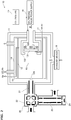
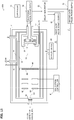
- Fig. 1 is an illustrative diagram schematically showing a construction of the nanocluster production apparatus 10.
- the nanocluster production apparatus 10 has a chamber 11, which is vacuumed, a nanocluster growth cell 12 installed in the chamber 11 and a sputtering source 13 (magnetron sputtering source) installed in the nanocluster growth cell 12.
- the nanocluster growth cell 12 according to the present embodiment is surrounded by a liquid nitrogen jacket 14. Liquid nitrogen (N 2 ) flows through the inside of the liquid nitrogen jacket 14.
- the nanocluster production apparatus 10 further has a controller 15 and a sputtering pulse power supply 16 as constituent components of a control system.
- the nanocluster production apparatus 10 further has a first inert gas supply pipe 17 for supplying a first inert gas (for instance, argon gas (Ar)), which is used for generating plasma, to the sputtering source 13 and a second inert gas supply pipe 18 for supplying a second inert gas (for instance, helium gas (He)) into the nanocluster growth cell 12.
- the second inert gas is used for cooling and condensing neutral atoms and ions generating from the sputtering source 13 and for causing them to grow into nanoclusters.
- a main part of the second inert gas supply pipe 18 is housed in the liquid nitrogen jacket 14 and goes around spirally inside the liquid nitrogen jacket 14.
- a tip end of the second inert gas supply pipe 18 projects to an inside of the nanocluster growth cell 12.
- the second inert gas such as the helium cooled by the liquid nitrogen can be introduced into the nanocluster growth cell 12.
- Pressure in the cluster growth cell 12 is maintained at approximately 2 to 40 Pa.
- Devices such as a pressure gauge connected to the cluster growth cell 12 for pressure control and a mass flow controller connected to the gas supply system are not shown in the drawings.
- the nanocluster production apparatus 10 further has an exhaust device 19 constituted by a turbo-molecular pump and the like. With the exhaust device 19, the inside of the chamber 11 is evacuated to a predetermined pressure (for instance, 10 -1 to 10 -4 Pa).
- a predetermined pressure for instance, 10 -1 to 10 -4 Pa.
- the sputtering source 13 is constituted by a target 131 (for instance, metal target), an anode 132 and a magnet unit 133.
- the target 131 is connected to the sputtering pulse power supply 16 and serves as a cathode.
- a pulsed electric power is supplied from the sputtering pulse power supply 16 (that is, pulsed high voltage is applied between target 131 and anode 132)
- a glow discharge arises between the target 131 and the anode 132.
- the nanocluster production apparatus 10 according to the present example applies a magnetic field near the surface of the target 131 using the magnet unit 133, thereby performing magnetron sputtering. Thus, a strong glow discharge can be generated.
- the tip end of the first inert gas supply pipe 17 is constructed to inject the first inert gas from one or more apertures between the target 131 and the anode 132 of the sputtering source 13.
- the present invention is not limited to such the construction. Any construction can be employed as long as the first inert gas can be supplied to head to the target 131.
- the sputtering source 13 is housed in the nanocluster growth cell 12 such that the sputtering source 13 can move freely in a tube axial direction.
- length of the nanocluster growth space in the tube axis direction i.e., growth space length, or distance from surface of target 131 to beam extraction aperture 121 is defined.
- the first inert gas is supplied to the sputtering source 13 and the pulsed power is supplied from the sputtering pulse power supply 16. If the pulsed power is supplied, sputtered particles such as neutral atoms and ions originating from the target 131 are emitted as a bunch from the target 131 into the second inert gas.
- This bunch is emitted at intervals of the repetition rate of the pulsed power applied to the sputtering source 13 and moves along the flow of the second inert gas.
- the sputtered particles such as the neutral atoms and ions constituting the bunch combine with each other in the second inert gas to produce the nanoclusters having various sizes.
- the produced nanoclusters pass through the beam extraction aperture 121 of the nanocluster growth cell 12 and then enter a subsequent ion detection device and the like.
- a detection device having a construction shown in Fig. 2 can be used, for instance.
- the ion detection device 20 shown in Fig. 2 has an ion guide electrode 21 outside a neighborhood of the beam extraction aperture 121 of the nanocluster growth cell 12.
- the ion detection device 20 has a quadrupole ion deflector 22 placed downstream of the ion guide electrode 21.
- the quadrupole ion deflector 22 deflects and extracts either cations or anions out of the nanoclusters.
- the nanocluster ions produced with the above-mentioned construction were detected with the ion detection device 20.
- the sputtering pulse power supply 16 used in this example performs the discharge repeatedly in ON and OFF periods (ON period: t ON , OFF period: T OFF ).
- MPP Modulated Pulse Power
- the sputtering pulse power supply 16 used in this example incorporates a pulse generator.
- the voltage DCV supplied from the power supply 16 can be controlled from 80 V to 600 V, and a peak voltage and a peak current change correspondingly.
- a peak discharge power is represented by the product of the peak voltage and the peak current.
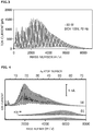
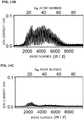
- Fig. 3 is an explanatory diagram for explaining a size distribution of Ag nanocluster cations produced with the nanocluster production apparatus 10.
- Fig. 3 shows a mass spectrum in the case where an average discharge power of the sputtering pulse power supply 16 is set at approximately 30 W, the supplied voltage DCV is set at 105 V and the repetition rate of the discharge is set at 70 Hz.
- the horizontal axis indicates the mass number per unit charge (m/Z), and the vertical axis indicates the ion current (pA) equivalent to the produced amount of the nanocluster ions.
- Fig. 4 shows a mass spectrum (a) of Ag nanocluster anions obtained by the modulated pulse power magnetron sputtering method using the modulated pulse power supply (hereinafter, referred to as MPP-MSP method) and a mass spectrum (b) of Ag nanocluster anions obtained by the direct-current magnetron sputtering method (DC-MSP method) in comparison.
- MPP-MSP method the repetition rate is set at 100 Hz
- the peak discharge power is set at 200 W
- the average discharge power is controlled to approximately 30 W.
- the discharge power is set at 30 W in the DC-MSP method.
- the flow rate of Ar is set to 100 sccm
- the flow rate of He is set to 600 sccm.
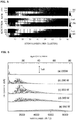
- Fig. 5 is a diagram showing that the ion intensity can be increased by controlling the parameters of the modulated pulse power supply.
- Fig. 5 shows the ion intensity of the Ag nanocluster anions in the case (a) where the discharge power is 370 W, the case (b) where the discharge power is 320 W and the case (c) where the discharge power is 210 W, respectively.
- the horizontal axis of the diagram indicates the number of the atoms per nanocluster, and the vertical axis indicates the repetition rate of the pulse discharge.
- a duration time of generation of each pulse discharge was set to be constant (approximately 1 ms).
- the duty ratio of the pulse discharge is proportional to the repetition rate (that is, duty ratio is approximately 0.007 to 0.15 with respect to repetition rate of 7 to 150 Hz). It can be understood from Fig. 5 that the ion intensity (obtained amount and yield) can be improved by two-dimensional control (optimization) of the peak discharge power and the repetition rate (or duty ratio) of the discharge.
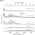
- Fig. 6 is an explanatory diagram for explaining an influence on the cluster size and the ion intensity in the case where the peak discharge power is changed in the MPP-MSP method.
- the size distributions of the Ag nanocluster anions in the cases where the peak discharge power is set to (a) 220 W, (b) 290 W, (c) 350 W, (d) 380 W and (e) 560 W respectively are shown in an offset manner.
- the flow rate of Ar was set to 120 sccm
- the flow rate of He was set to 600 sccm
- the discharge repetition rate was set to 10 Hz. It can be understood from Fig. 6 that the distribution of the cluster size changes depending on the peak discharge power, that is, there is a tendency that the distribution of the cluster size shifts toward a larger side as the peak discharge power increases.
- Fig. 8 is an explanatory diagram for explaining an influence of the cluster growth space length on the Ag nanocluster size and the ion intensity and shows the case (a) of 210 mm, the case (b) of 250 mm, and the case (c) of 280 mm respectively in an offset manner.
- the flow rate of Ar was set to 80 sccm
- the flow rate of He was set to 600 sccm
- the supplied voltage DCV was set to 90 V
- the repetition rate of the discharge was set to 70 Hz.
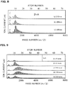
- Fig. 9 is an explanatory diagram for explaining an influence of the Ar gas flow rate on the Ag nanocluster size and the ion intensity and shows the cluster size distributions in the cases where the Ar gas flow rate is (a) 40 sccm, (b) 60 sccm, (c) 100 sccm, (d) 120 sccm and (e) 160 sccm respectively.
- the flow rate of the He gas was set to 600 sccm
- the cluster growth space length was set to 290 mm
- the supplied voltage DCV was set to 90 V
- the repetition rate of the discharge was set to 70 Hz.
- Fig. 10 is an explanatory diagram for explaining an influence of the change of the He gas flow rate on the Ag nanocluster size and the ion intensity and shows the cluster size distributions in the cases where the He gas flow rate is (a) 140 sccm, (b) 200 sccm, (c) 400 sccm and (d) 600 sccm respectively in an offset manner.
- the flow rate of the Ar gas was set to 80 sccm
- the cluster growth space length was set to 290 mm
- the supplied voltage DCV was set to 90 V
- the repetition rate of the discharge was set to 70 Hz.
- the nanocluster production apparatus 10 uses the magnetron sputtering method for applying the pulsed power. Therefore, the size selectivity of the produced nanoclusters improves and the obtained amount and the yield improve as compared to the conventional direct-current power magnetron sputtering method.
- the size selectivity of the produced nanoclusters can be improved by controlling the repetition rate of the pulsed power, the peak discharge power or the pulse waveform (duty ratio).
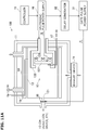
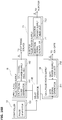
- the nanocluster production apparatus 100 has a gate 30, which permits or prohibits passage of the nanocluster ions through the beam extraction aperture 121 of the nanocluster growth cell 12, a gate pulse power supply 31, and a delay generator 32 in addition to the construction of the nanocluster production apparatus 10 described before.
- the gate 30 is a metal mesh electrode, for instance, and is installed near the beam extraction aperture 121 of the nanocluster growth cell 12 in the chamber 11.
- the gate 30 is used to permit or prohibit the passage of only the nanocluster ions having either polarity among the nanocluster ions.
- the control system of the nanocluster production apparatus 100 is constituted by a controller 15, a sputtering pulse power supply 16, a delay generator 32, and the gate pulse power supply 31.
- the controller 15 has a pulse generator 151.
- a pulse generator may be incorporated in the sputtering pulse power supply 16.
- the sputtering pulse power supply 16 has a sputtering signal generator 161 and a sputtering power supply main unit 162.
- the gate pulse power supply 31 has a gate signal generator 311 and a gate power supply main unit 312.
- the pulse generator 151 When generating the nanoclusters, the pulse generator 151 generates a pulsed clock signal, and sends the clock signal to the sputtering signal generator 161 of the sputtering pulse power supply 16.
- the sputtering signal generator 161 If the sputtering signal generator 161 receives the clock signal, the sputtering signal generator 161 generates a pulsed sputtering signal, sends the sputtering signal to the sputtering power supply main unit 162 and sends a synchronization signal to the delay generator 32.
- the sputtering power supply main unit 162 applies a pulsed high voltage to the sputtering source 13 while the sputtering signal is ON.
- the delay generator 32 If the delay generator 32 receives the synchronization signal, the delay generator 32 generates a delay signal, which has a predetermined delay based on the synchronization signal, and sends the delay signal to the gate pulse power supply 31. If the gate signal generator 311 of the gate pulse power supply 31 receives the delay signal, the gate signal generator 311 generates a pulsed gate signal and sends the gate signal to the gate power supply main unit 312.
- the gate power supply main unit 312 applies a voltage to the gate according to the gate signal. For instance, the gate power supply main unit 312 applies a positive or negative voltage to the gate 30 while the gate signal is OFF.
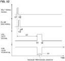
- the sputtering signal generator 161 sends a synchronization signal to the delay generator 32 at the time s1.
- the delay generator 32 generates a delay signal, which has a predetermined delay based on the received synchronization signal, and sends the delay signal to the gate pulse power supply 31.
- the gate signal generator 311 of the gate pulse power supply 31 receives the delay signal, the gate signal generator 311 generates a pulsed gate signal (t1 to t2) and sends the gate signal to the gate power supply main unit 312.
- the gate power supply main unit 312 applies the voltage to the gate 30 according to the gate signal. In this example, a positive voltage +V is applied to the gate while the gate signal is OFF, and the voltage applied to the gate is set to 0 V only while the gate signal is ON.
- the cluster cations emitted from the beam extraction aperture 121 of the cluster growth cell 12 are rejected by the gate 30 and cannot pass through the gate 30. Only while the potential of the gate 30 is 0 V, the cluster cations can pass through the gate 30 and enter the subsequent ion detection device or the like.
- the time frame (t1 to t2), in which the potential of the gate 30 is set to 0 V to permit the passage of the cluster ions having the polarity as the object of permission or prohibition of passage in this way, will be referred to as a passage permission window hereinafter.
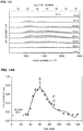
- FIG. 13 A result of measurement of the size of the Ag nanocluster anion performed with the subsequent ion detection device (for instance, ion detection device 20 shown in Fig. 1 ) while changing in various ways the delay ⁇ t from the rising time s1 of the sputtering signal to the rising time t1 of the gate signal in the above construction is shown in Fig. 13.
- Fig. 13 A result of measurement of the size of the Ag nanocluster anion performed with the subsequent ion detection device (for instance, ion detection device 20 shown in Fig. 1 ) while changing in various ways the delay ⁇ t from the rising time s1 of the sputtering signal to the rising time t1 of the gate signal in the above construction is shown in Fig. 13.
- Fig. 13 A result of measurement of the size of the Ag nanocluster anion performed with the subsequent ion detection device (for instance, ion detection device 20 shown in Fig. 1 ) while changing in various ways the delay ⁇ t from the rising time s1 of the
- FIG. 13 is a diagram, in which size distributions of the nanocluster ions at respective elapsed times after the rising time s1 of the sputtering signal are plotted and which shows the results at the elapsed times of 0 ms, 40 ms, 50 ms, 60 ms, 70 ms, 90 ms, 100 ms, and 140 ms respectively in this order from the bottom.
- the size distribution of the detected cluster ions changes as the time elapses after the sputtering signal is emitted and the pulse discharge starts. That is, it is understood that the cluster size has a time distribution.
- the cluster growth space length was set to 290 mm
- the supplied voltage was set to 120 V
- the repetition rate was set to 7 Hz
- the passage permission window was set to 4 ms.
- the ion current near the mass number of 4000 is high in the range of 50 ms to 70 ms, once becomes low at 90 ms and increases again at 100 ms in Fig. 13 .
- Fig. 14A is a diagram, in which the ion amount detected at each time during a single pulse discharge period is plotted with a black dot along a vertical axis, with a horizontal axis indicating an arrival time at the gate 30 after the sputtering on the target 131 is started.
- a solid curve is a guide for eyes.
- the nanocluster beams having the size distribution controlled with high accuracy can be obtained.
- the obtained amount of the nanocluster beams having the size distribution controlled with high accuracy can be increased.
- the gate 30 is the metal mesh in the example of Fig. 11A but the present invention is not limited thereto. That is, any device that can permit or prohibit the passage of the cluster ions or that can change a flight trajectory of the nanocluster ions by using an electric field, a magnetic field or an electromagnetic field (for instance, deflector, Wien filter and the like) can be used as the gate 30. Furthermore, if the neutral nanoclusters are ionized by laser irradiation, electron irradiation or the like, an operation to permit or prohibit the passage of the nanocluster ions originating from the neutral clusters can be also performed with the gate 30.
- a device that can perform an operation to prohibit or permit the passage of the beam by blocking or unblocking the flight trajectory of the beam physically for instance, shutter
- a device that changes the flight trajectory of the beam physically for instance, gas injector capable of performing pulse injection of gas
- a mechanical device such as a disk that has a predetermined slit/slits and that can rotate at high speed.
- Such devices can be used as the gate for both of the neutral nanoclusters and the nanocluster ions.
- the nanocluster production apparatus 200 is characterized by having a gate also inside the cluster growth cell 12. That is, as shown in Fig. 15 , the nanocluster production apparatus 200 has a first gate 40 installed inside the cluster growth cell 12 and a second gate 50 installed near the beam extraction aperture 121 of the cluster growth cell 12 as gates. Further, the nanocluster production apparatus 200 has a first gate pulse power supply 41 for the first gate 40 and a second gate pulse power supply 51 for the second gate 50.
- the nanocluster production apparatus 200 has a metallic ground shield 42 (for instance, metal mesh) covering the first gate 40.
- the potential of the ground shield 42 is set to the same potential as the cluster growth cell 12.
- the first gate 40 extends near the center of the interior space of the cluster growth cell 12.
- the interior space of the cluster growth cell 12 is divided by the first gate 40 into an upstream space and a downstream space.
- the passage of the nanocluster ions, which have grown in the upstream space, through the first gate 40 can be permitted or prohibited by performing control of the first gate 40 similar to the control explained in the description of the second embodiment. That is, by setting a predetermined passage permission window for the first gate 40, only nanocluster cations or nanocluster anions having a specific size distribution can be selectively caused to pass through the first gate 40.
- the interior space of the cluster growth cell 12 downstream of the first gate 40 is constructed as a space for controlling the flight trajectory or velocity of the nanocluster ions having passed through the first gate 40.
- the construction shown in Fig. 15 performs promotion or suppression of the growth of the nanocluster ions or selection and control of the size or the structure of the nanocluster ions by accelerating or decelerating the passing nanocluster ions or by changing the flight trajectory of the passing nanocluster ions using a difference in the mass or in the degree of movement of the nanocluster ions with multiple ion motion control electrodes 60 installed inside the cluster growth cell 12.
- the ion motion control electrodes 60 are controlled by applying a voltage with an ion motion controller 61.
- the ion motion controller 61 is controlled by a control signal emitted from the delay generator 32 in synchronization with the sputtering signal.
- the method of controlling the flight trajectory or the velocity of the nanocluster ions is not limited to the above. Any construction may be used as long as the construction can control the flight trajectory or the velocity of the nanocluster ions.
- the nanocluster production apparatus 300 has an injector 70 for injecting an Ar gas as the first inert gas and an injector pulse power supply 71 that controls an operation of the injector 70 in addition to the construction of the nanocluster production apparatus (10).
- an injector 70 for injecting an Ar gas as the first inert gas
- an injector pulse power supply 71 that controls an operation of the injector 70 in addition to the construction of the nanocluster production apparatus (10).
- pulse injection of the Ar gas can be performed.
- the injector 70 is installed outside the chamber 11, and the pulsed power is supplied from the injector pulse power supply 71 to the injector 70, whereby the Ar gas can be injected intermittently through the first inert gas supply pipe 17.
- the Ar gas injected from the opening of the first inert gas supply pipe 17 shoots from a spot or spots of the inner peripheral surface of the anode 132 near the sputtering surface of the target 131 substantially in parallel with the target 131 and spreads at a predetermined angle.
- the Ar gas is supplied from a high-pressure gas feed unit (not shown) to the injector 70.
- the high-pressure gas feed unit consists of an Ar gas tank storing the Ar gas, a pressure regulator and the like, for instance.
- An automotive fuel injector e.g., injector for diesel engine
- injector 70 can be used as the injector 70, for instance.
- an electromagnetic injector or a piezo injector may be used as the injector 70, for instance. Any injector of any system may be used if it can perform a drive described below.
- the control system of the nanocluster production apparatus 300 is constituted by a controller 15, a sputtering pulse power supply 16, a delay generator 32, a gate pulse power supply 31 and an injector pulse power supply 71 as shown in Fig. 16B .
- the injector pulse power supply 71 has an injection signal generator 711 and an injector power supply main unit 712. The other construction is the same as that of the second embodiment.
- the pulse generator 151 generates a pulsed clock signal and sends the clock signal to the delay generator 32.
- the delay generator 32 is a multichannel delay unit and generates a first delay signal having a first delay based on the clock signal, a second delay signal having a second delay different from the first delay and a third delay signal having a further different third delay.
- the delay generator 32 sends the first delay signal to the sputtering pulse power supply 16, sends the second delay signal to the injector pulse power supply 71 and sends the third delay signal to the gate pulse power supply 31.
- the sputtering signal generator 161 of the sputtering pulse power supply 16 receives the first delay signal, it generates a pulsed sputtering signal and sends the sputtering signal to the sputtering power supply main unit 162.
- the sputtering power supply main unit 162 applies a pulsed high voltage to the sputtering source 13 while the sputtering signal is ON.
- the injection signal generator 711 of the injector pulse power supply 71 receives the second delay signal, it generates a pulsed injection signal and sends the injection signal to the injector power supply main unit 712.
- the injector power supply main unit 712 supplies a pulsed power to the injector 70 according to the injection signal (for instance, it applies voltage to injector 70 while injection signal is ON).
- an actuator of the injector 70 starts driving.
- injection of the Ar gas from an injection hole of the injector 70 starts at time r3 when a delay passes after the time r1.
- the injection signal changes to OFF at time r2
- the injection of the Ar gas ends at time r4 when a delay passes.
- the delay generator 32 suitably controls the transmission start time s1 of the sputtering signal and the transmission start time r1 of the injection signal with the first and second delay signals
- the sputtering signal generator 161 suitably controls the transmission end time s2 of the sputtering signal (or duration of sputtering signal)
- the injection signal generator 711 suitably controls the transmission end time r2 of the injection signal (or duration of injection signal) such that the entire period s3 to s4, in which the pulse discharge actually occurs, is included in the period r3 to r4, in which the Ar gas is actually injected.
- the pulse discharge can be caused in the state where the sufficient amount of the Ar gas for the sputtering is supplied to the target 131.
- the injection of the Ar gas can be continued to timing after the completion of the sputtering.
- blockage of the injection hole of the injector 70 due to deposition of the sputtered particles (metal particles and the like) can be inhibited with the flow of the Ar gas that continues to shoot from the injection hole of the injector 70.
- the duty ratio of the injector 70 ratio of time in which injector 70 actually injects
- the tip end of the first inert gas supply pipe 17 is constructed to inject the first inert gas from one or more spots between the target 131 and the anode 132 of the sputtering source 13.
- the present invention is not limited thereto. Alternatively, any construction can be employed as long as the construction can supply the first inert gas such that the first inert gas heads to the target 131.
- the injector 70 may be installed in the chamber 11, in the cluster growth cell 12 or in the sputtering source 13.
- the sputtering signal emitted by the sputtering signal generator 161 of the sputtering pulse power supply 16 is a single pulse signal (refer to Fig. 12 ).
- the sputtering signal may be emitted as a signal group composed of multiple micro pulse signals as shown in an upper part of Fig. 18 .
- the sputtering signal generator 161 may be constructed with a micro pulse generator.
- a modulated pulse power supply can be used.
- pulse width of each micro pulse signal may be approximately 10 microseconds.
- a plurality of the micro pulse signals are emitted successively to emit a sputtering signal as a signal group that extends for a period of approximately 100 microseconds to 3 milliseconds as a whole.
- the sputtering power supply main unit 162 supplies the power to the sputtering source 13 according to the received sputtering signal.
- the supplied power can be varied during the discharge period of each cycle by controlling the respective micro pulse signals.
- frequency of the micro pulse signals is set relatively low in the period from s1 to s2 (i.e., micro pulse signal group is made sparse), and the frequency of the micro pulse signals is set relatively high during the period from s2 to s3 (i.e., micro pulse signal group is made dense).
- the power supplied to the sputtering source 13 takes a relatively low value during the period from s4 to s5 in an early stage of the application of the power and takes a relatively high value during the period from s5 to s6 after that and until the end of the application of the power.
- plasma based on Ar can be lit by a relatively weak discharge in the early stage of the discharge, and a larger volume of the plasma can be generated in a later stage of the discharge.
- Such the mode of the generation of the plasma is desirable for generation of more stable plasma and also for discharge of a larger amount of the sputtered particles.
- the present invention is not limited to varying the frequency of the micro pulse signals. Alternatively, or in addition to it, a duty ratio of the micro pulse signals may be varied.
- a voltage value of the sputtering power supply main unit 162 may be varied.
- the injection signal generator 711 may be also constructed with a micro pulse generator like the sputtering signal generator 161.
- the sputtering source 13 is installed in the cluster growth cell 12, but the present invention is not limited thereto. That is, the sputtering source 13 may be arranged outside the cluster growth cell 12 as long as the sputtering source 13 is inside the chamber 11 and the sputtered particles sputtered from the target 131 of the sputtering source 13 can promptly enter the inside of the cluster growth cell 12 immediately after being sputtered.
- ground shield 42 which is used in the second embodiment shown in Fig. 15 , for the gates 30, 50 installed near the beam extraction aperture 121 of the cluster growth cell 12 to avoid influence on the upstream or downstream potential.
- the cooling jacket 14 using the liquid nitrogen is used, but the present invention is not limited thereto.
- a construction for introducing the liquid helium into the cluster growth cell 12 may be employed and the cooling jacket 14 may be omitted. Also in this case, similar effects about the production and the growth of the nanoclusters can be acquired.
- FIG. 19 Another working example of the present invention is shown in Fig. 19 .
- a result of an experiment for production of TaSi composite nanocluster ions using the construction of Figs. 11A , 11B is shown.
- a target made by pressing powder of TaSi alloy (Ta: 16 wt%) was used as the target 131.
- Fig. 19 is a diagram showing temporal change of generation intensity of the TaSi composite nanocluster cations. Experimental conditions are as follows.
- a vertical axis on the right side indicates the delay ⁇ t shown in Fig. 12
- a horizontal axis indicates the size (mass number) of the detected nanocluster.
- Another vertical axis on the left side indicates detection intensity (arbitrary unit) of the nanocluster.
- the nanocluster beam having the composition and the size distribution controlled with high accuracy can be obtained by changing the delay ⁇ t and by permitting the passage of the nanocluster ions only in the predetermined time window synchronized with the pulse discharge.
- the nanocluster production technique using the nanocluster production apparatus according to the present invention can be applied also to the nonmetallic target and that the technique can be applied also to the two-component composite.
Landscapes
- Chemical & Material Sciences (AREA)
- Engineering & Computer Science (AREA)
- Analytical Chemistry (AREA)
- Physics & Mathematics (AREA)
- Plasma & Fusion (AREA)
- Chemical Kinetics & Catalysis (AREA)
- Materials Engineering (AREA)
- Mechanical Engineering (AREA)
- Metallurgy (AREA)
- Organic Chemistry (AREA)
- Physical Vapour Deposition (AREA)
Claims (16)
- Nanocluster-Herstellungsvorrichtung (100, 200, 300) mit:einer Vakuumkammer (11);einer Sputterquelle (13), die daran angepasst ist, durch gepulste Entladung ein Plasma zu erzeugen;einer Pulsstromversorgung (16), die daran angepasst ist, der Sputterquelle (13) einen gepulsten Strom zuzuführen;einer Zufuhreinrichtung für erstes Inertgas (17), die daran angepasst ist, der Sputterquelle (13) ein erstes Inertgas zuzuführen;einer Cluster-Wachstumszelle (12), die in der Vakuumkammer (11) gelagert ist;einer Einleitungseinrichtung für zweites Inertgas (18), die daran angepasst ist, in die Cluster-Wachstumszelle (12) ein zweites Inertgas einzuleiten; undeiner Steuerung (15), wobeidie Cluster-Wachstumszelle (12) eine Strahlentnahmeöffnung (121) hat, die daran angepasst ist, die in der Cluster-Wachstumszelle (12) hergestellten Nanocluster als einen Strahl zu entnehmen,dadurch gekennzeichnet, dassdie Nanocluster-Herstellungsvorrichtung (100, 200, 300) außerdem eine Sperre (30) hat, die so gestaltet ist, dass sie die Entnahme des Strahls aus der Strahlentnahmeöffnung (121) gestattet oder unterbindet, unddie Steuerung (15) so gestaltet ist, dass sie einen Zeitpunkt der Sperre (30) zum Umschalten zwischen dem Gestatten und dem Unterbinden der Entnahme des Strahls aus der Strahlentnahmeöffnung (121) derart einstellt, dass der Zeitpunkt der Sperre durch den Startzeitpunkt der Zufuhr des gepulsten Stroms zur Sputterquelle ausgelöst wird.
- Nanocluster-Herstellungsvorrichtung (100, 200, 300) wie im Anspruch 1, wobei die Steuerung (15) derart gestaltet ist, dass sie die Pulsstromversorgung so steuert, dass sie eine Einschaltdauer des gepulsten Stroms und einen Spitzenentladungsstrom ändert.
- Nanocluster-Herstellungsvorrichtung (100, 200, 300) wie im Anspruch 2, wobei
die Sputterquelle ein Target (131) als eine Kathode hat,
eine Sputteroberfläche des Targets (131) und eine Innenfläche der Cluster-Wachstumszelle (12) einen Cluster-Wachstumsraum für ein Wachstum von Nanoclustern definieren, und
die Steuerung (15) so gestaltet ist, dass sie die Einschaltdauer des gepulsten Stroms und/oder den Spitzenentladungsstrom gemäß einer Länge des Cluster-Wachstumsraums, die durch einen Abstand von der Sputteroberfläche des Targets (131) bis zur Strahlentnahmeöffnung (121) definiert ist, und/oder Temperatur und Druck des zweiten Inertgases in der Cluster-Wachstumszelle (12) ändert. - Nanocluster-Herstellungsvorrichtung (100, 200, 300) wie im Anspruch 1 oder 2, wobei die Steuerung (15) so gestaltet ist, dass sie die Pulsstromversorgung (16) so steuert, dass sie eine Wiederholungsrate des gepulsten Stroms ändert.
- Nanocluster-Herstellungsvorrichtung (100, 200, 300) wie im Anspruch 4, wobei
die Sputterquelle ein Target (131) als eine Kathode hat,
eine Sputteroberfläche des Targets (131) und eine Innenfläche der Cluster-Wachstumszelle (12) einen Cluster-Wachstumsraum für ein Wachstum von Nanoclustern definieren, und
die Steuerung (15) so gestaltet ist, dass sie die Wiederholungsrate des gepulsten Stroms gemäß einer Länge des Cluster-Wachstumsraums, die durch einen Abstand von der Sputteroberfläche des Targets (131) bis zur Strahlentnahmeöffnung (121) definiert ist, und/oder Temperatur und Druck des zweiten Inertgases in der Cluster-Wachstumszelle (12) ändert. - Nanocluster-Herstellungsvorrichtung (100, 200, 300) wie in einem der Ansprüche 1 bis 5, wobei die Steuerung (15) so gestaltet ist, dass sie eine Dauer zum Gestatten der Entnahme des Strahls und eine Dauer zum Unterbinden der Entnahme des Strahls aus der Strahlentnahmeöffnung (121) als ein regelmäßiges Muster einstellt, das mit der gepulsten Entladung synchronisiert ist, und das Gestatten und das Unterbinden der Entnahme des Strahls aus der Strahlentnahmeöffnung (121) gemäß dem eingestellten Muster und synchron mit einer Wiederholungsdauer des gepulsten Stroms wiederholt.
- Nanocluster-Herstellungsvorrichtung (100, 200, 300) wie in einem der Ansprüche 1 bis 6, wobei die Steuerung (15) so gestaltet ist, dass sie den Zeitpunkt zum Umschalten zwischen dem Gestatten und dem Unterbinden der Entnahme des Strahls ändert, wodurch die Größe und/oder der Aufbau der Nanocluster, die durch die Strahlentnahmeöffnung (121) hindurch entnommen werden, gesteuert wird.
- Nanocluster-Herstellungsvorrichtung (100, 200, 300) wie in einem der Ansprüche 1 bis 7, wobei die Sperre (30) so gestaltet ist, dass sie die Entnahme des Strahls aus der Strahlentnahmeöffnung mit einem elektrischen Feld, einem magnetischen Feld oder einem elektromagnetischen Feld gestattet oder unterbindet.
- Nanocluster-Herstellungsvorrichtung (100, 200, 300) wie in einem der Ansprüche 1 bis 7, wobei die Sperre (30) so gestaltet ist, dass sie die Entnahme des Strahls aus der Strahlentnahmeöffnung (121) gestattet oder unterbindet, indem sie eine Flugbahn des Strahls ändert, blockiert oder freigibt.
- Nanocluster-Herstellungsvorrichtung (100, 200, 300) wie in einem der Ansprüche 1 bis 9, mit zudem einer anderen, innerhalb der Cluster-Wachstumszelle installierten Sperre (50), die so gestaltet ist, dass sie den Durchgang der Nanocluster gestattet oder unterbindet.
- Nanocluster-Herstellungsvorrichtung (100, 200, 300) wie in einem der Ansprüche 1 bis 10, wobei das erste Inertgas ein Argon-Gas ist.
- Nanocluster-Herstellungsvorrichtung (100, 200, 300) wie in einem der Ansprüche 1 bis 11, wobei das zweite Inertgas ein Helium-Gas ist.
- Nanocluster-Herstellungsvorrichtung (100, 200, 300) wie in einem der Ansprüche 1 bis 12, wobei
die Zufuhreinrichtung für erstes Inertgas (17) aus einem Gasinjektor für das erste Inertgas besteht und
die Steuerung (15) so gestaltet ist, dass sie die Sputterquelle (13) und den Gasinjektor derart steuert, dass der Gasinjektor das erste Inertgas intermittierend und derart injiziert, dass eine Dauer, in der in der Sputterquelle die Pulsentladung auftritt, in einer Dauer enthalten ist, in der der Gasinjektor das erste Inertgas injiziert. - Nanocluster-Herstellungsvorrichtung (100, 200, 300) wie im Anspruch 13, wobei
die Steuerung (15) so gestaltet ist, dass sie dem Gasinjektor gemäß einem Injektionssignal, das ein gepulstes elektrisches Signal ist, einen Strom zuführt, wodurch der Gasinjektor so angesteuert wird, dass er das erste Inertgas injiziert,
die Steuerung (15) so gestaltet ist, dass sie das Injektionssignal mit einer Gruppe von einer Vielzahl von Pulssignalen aufbaut, und
die Steuerung (15) so gestaltet ist, dass sie eine Einschaltdauer oder Frequenz der Vielzahl von Pulssignalen in der das Injektionssignal aufbauenden Gruppe ändert. - Nanocluster-Herstellungsvorrichtung (100, 200, 300) wie in einem der Ansprüche 1 bis 14, wobei
die Steuerung (15) so gestaltet ist, dass sie der Sputterquelle (13) gemäß einem Sputtersignal, das ein gepulstes elektrisches Signal ist, einen gepulsten Strom zuführt,
die Steuerung (15) so gestaltet ist, dass sie das Sputtersignal mit einer Gruppe von einer Vielzahl von Pulssignalen aufbaut, und
die Steuerung (15) so gestaltet ist, dass sie eine Einschaltdauer oder Frequenz der Vielzahl von Pulssignalen in der das Sputtersignal aufbauenden Gruppe ändert. - Nanocluster-Herstellungsvorrichtung (100, 200, 300) wie in einem der Ansprüche 1 bis 15, wobei das zweite Inertgas als ein Kühlmittelgas dient, um die gesputterten Partikel zu kühlen, die von der Sputterquelle aus injiziert werden.
Applications Claiming Priority (2)
| Application Number | Priority Date | Filing Date | Title |
|---|---|---|---|
| JP2013112995A JP5493139B1 (ja) | 2013-05-29 | 2013-05-29 | ナノクラスター生成装置 |
| PCT/JP2014/063877 WO2014192703A1 (ja) | 2013-05-29 | 2014-05-26 | ナノクラスター生成装置 |
Publications (3)
| Publication Number | Publication Date |
|---|---|
| EP3006594A1 EP3006594A1 (de) | 2016-04-13 |
| EP3006594A4 EP3006594A4 (de) | 2017-01-04 |
| EP3006594B1 true EP3006594B1 (de) | 2018-03-28 |
Family
ID=50792319
Family Applications (1)
| Application Number | Title | Priority Date | Filing Date |
|---|---|---|---|
| EP14803503.3A Active EP3006594B1 (de) | 2013-05-29 | 2014-05-26 | Vorrichtung zur herstellung von nanoclustern |
Country Status (4)
| Country | Link |
|---|---|
| US (1) | US10283333B2 (de) |
| EP (1) | EP3006594B1 (de) |
| JP (1) | JP5493139B1 (de) |
| WO (1) | WO2014192703A1 (de) |
Families Citing this family (7)
| Publication number | Priority date | Publication date | Assignee | Title |
|---|---|---|---|---|
| WO2016036739A1 (en) * | 2014-09-05 | 2016-03-10 | Tel Epion Inc. | Process gas enhancement for beam treatment of a substrate |
| WO2017030087A1 (ja) * | 2015-08-17 | 2017-02-23 | 国立研究開発法人科学技術振興機構 | ナノクラスター分散液、ナノクラスター膜、ナノクラスター分散体、ナノクラスター分散液の製造方法およびナノクラスター分散液の製造装置 |
| WO2018038098A1 (ja) * | 2016-08-22 | 2018-03-01 | 国立研究開発法人科学技術振興機構 | メモリデバイス |
| US11094515B2 (en) | 2016-12-19 | 2021-08-17 | Panasonic Intellectual Property Management Co., Ltd. | Sputtering apparatus and sputtering method |
| ES2883375T3 (es) * | 2018-07-31 | 2021-12-07 | Consejo Superior Investigacion | Dispositivo para la fabricación estable de nanoagregados |
| WO2021251395A1 (ja) | 2020-06-08 | 2021-12-16 | 学校法人慶應義塾 | 担持体、担持体の製造装置及び担持体の製造方法 |
| CN114318280B (zh) * | 2021-12-02 | 2023-12-01 | 北京航空航天大学合肥创新研究院(北京航空航天大学合肥研究生院) | 一种用于测量和控制纳米团簇生长的方法 |
Family Cites Families (21)
| Publication number | Priority date | Publication date | Assignee | Title |
|---|---|---|---|---|
| JPS61261473A (ja) | 1985-05-15 | 1986-11-19 | Tokuda Seisakusho Ltd | スパツタリング装置 |
| US5126028A (en) * | 1989-04-17 | 1992-06-30 | Materials Research Corporation | Sputter coating process control method and apparatus |
| CH687258A5 (de) * | 1993-04-22 | 1996-10-31 | Balzers Hochvakuum | Gaseinlassanordnung. |
| JP3360102B2 (ja) | 1996-12-10 | 2002-12-24 | 日本航空電子工業株式会社 | イオンビームスパッタ装置 |
| JP2957161B1 (ja) | 1998-04-27 | 1999-10-04 | 株式会社 つくばクラスター研究所 | クラスターの生成方法及びその装置 |
| JP2000144392A (ja) * | 1998-11-06 | 2000-05-26 | Canon Inc | 薄膜形成装置及び薄膜形成方法 |
| JP2001011621A (ja) | 1999-06-30 | 2001-01-16 | Hitachi Ltd | マグネトロンスパッタ装置 |
| JP3398352B2 (ja) * | 2000-01-20 | 2003-04-21 | 株式会社つくばナノ・テクノロジー | クラスターイオンビーム発生装置 |
| US20060222790A1 (en) * | 2003-07-30 | 2006-10-05 | The Regents Of The University Of California | Preparation of library that includes monodisperse nanoclusters |
| CN102064367B (zh) * | 2003-12-08 | 2013-01-30 | 松下电器产业株式会社 | 半导体电极及其制造方法、和使用该半导体电极的光电池 |
| JP5273495B2 (ja) * | 2005-12-13 | 2013-08-28 | 独立行政法人産業技術総合研究所 | クラスター成膜装置及び成膜方法、並びにクラスター生成装置及び生成方法 |
| JP2007327095A (ja) * | 2006-06-07 | 2007-12-20 | Toyota Motor Corp | 金属クラスター生成装置 |
| JP4960694B2 (ja) * | 2006-12-21 | 2012-06-27 | 株式会社リコー | トナーの製造方法、トナー、2成分現像剤、プロセスカートリッジ、及び画像形成装置 |
| JP2008260999A (ja) | 2007-04-11 | 2008-10-30 | Toyota Motor Corp | クラスターの生成方法および装置 |
| FR2924359B1 (fr) * | 2007-11-30 | 2010-02-12 | Commissariat Energie Atomique | Procede de preparation de depot de nanoparticules metalliques par depot physique en phase vapeur |
| GB2473655A (en) | 2009-09-21 | 2011-03-23 | Mantis Deposition Ltd | Magnetron sputtering techiques and apparatus |
| SE535381C2 (sv) * | 2010-02-24 | 2012-07-17 | Plasmadvance Ab | Plasmasputtringsprocess för att producera partiklar |
| US8338806B2 (en) * | 2010-05-05 | 2012-12-25 | Tel Epion Inc. | Gas cluster ion beam system with rapid gas switching apparatus |
| JP5683902B2 (ja) | 2010-10-29 | 2015-03-11 | 株式会社東芝 | レーザ・イオン源 |
| CN102779140B (zh) * | 2011-05-13 | 2015-09-02 | 富士通株式会社 | 一种关键词获取方法及装置 |
| JP2013096004A (ja) * | 2011-11-07 | 2013-05-20 | Hitachi Tool Engineering Ltd | 耐剥離性に優れる被覆工具およびその製造方法 |
-
2013
- 2013-05-29 JP JP2013112995A patent/JP5493139B1/ja active Active
-
2014
- 2014-05-26 US US14/893,775 patent/US10283333B2/en active Active
- 2014-05-26 EP EP14803503.3A patent/EP3006594B1/de active Active
- 2014-05-26 WO PCT/JP2014/063877 patent/WO2014192703A1/ja not_active Ceased
Non-Patent Citations (1)
| Title |
|---|
| None * |
Also Published As
| Publication number | Publication date |
|---|---|
| JP2015045031A (ja) | 2015-03-12 |
| EP3006594A4 (de) | 2017-01-04 |
| JP5493139B1 (ja) | 2014-05-14 |
| WO2014192703A1 (ja) | 2014-12-04 |
| US10283333B2 (en) | 2019-05-07 |
| US20160111262A1 (en) | 2016-04-21 |
| EP3006594A1 (de) | 2016-04-13 |
Similar Documents
| Publication | Publication Date | Title |
|---|---|---|
| EP3006594B1 (de) | Vorrichtung zur herstellung von nanoclustern | |
| Ryabchikov et al. | High intensity metal ion beam generation | |
| JPH03503695A (ja) | 特にガスレーザーのx線‐前期電離のためのプラズマx線管、このx線管によるx線放射の発生方法および用途 | |
| Burdakov et al. | Development of extended heating pulse operation mode at GOL-3 | |
| Brown et al. | Vacuum arc ion sources: Recent developments and applications | |
| Gushenets et al. | Current status of plasma emission electronics: I. Basic physical processes | |
| Li et al. | Study on electrons conduction paths in Hall thruster ignition processes with the cathode located inside and outside the magnetic separatrix | |
| RU92240U1 (ru) | Устройство для нанесения оксидных композиционных покрытий | |
| Batalin et al. | Electron-beam enhancement of the metal vapor vacuum arc ion source | |
| Abdrashitov et al. | Operation of RF driven negative ion source in a pure-hydrogen mode | |
| Abdrashitov et al. | Negative ion production in the RF multiaperture surface-plasma source | |
| Belchenko et al. | Development of surface-plasma negative ions sources at the Budker Institute of nuclear physics | |
| Yushkov et al. | A forevacuum plasma source of pulsed electron beams | |
| Ryabchikov et al. | Sources and methods of repetitively pulsed ion/plasma material treatment | |
| Gleizer et al. | Optimization of a low-pressure hollow-anode electrical discharge for generation of high-current electron beams | |
| Nikolaev et al. | Production of multiply charged bismuth ion beams in a vacuum arc ion source with a submicrosecond pulse duration | |
| Gushenets et al. | Nanosecond high current and high repetition rate electron source | |
| JP2010248574A (ja) | 蒸着装置及び蒸着方法。 | |
| Tiron et al. | „The effect of the additional magnetic field and gas pressure on the sheath region of a high power impulse magnetron sputtering discharge” | |
| Grabovskiĭ et al. | Influence of the current growth rate on the polarity effect in a wire array in the Angara-5-1 facility | |
| Viktorov et al. | Excitation of electromagnetic waves in dense plasma during the injection of supersonic plasma flows into magnetic arch | |
| Gavrilov et al. | Plasma cathode for a broad-beam electron accelerator | |
| Debolt et al. | Recent results from the low inductance Z-discharge metal vapor ion source | |
| Yoshitama et al. | Self-injection and acceleration of monoenergetic electron beams from laser wakefield accelerators in a highly relativistic regime | |
| Semenov et al. | Properties of Low Pressure Magnetron Discharge Under the Initiation of Emission Processes on Discharge Electrodes by An Accelerated Ion Beam |
Legal Events
| Date | Code | Title | Description |
|---|---|---|---|
| PUAI | Public reference made under article 153(3) epc to a published international application that has entered the european phase |
Free format text: ORIGINAL CODE: 0009012 |
|
| 17P | Request for examination filed |
Effective date: 20151127 |
|
| AK | Designated contracting states |
Kind code of ref document: A1 Designated state(s): AL AT BE BG CH CY CZ DE DK EE ES FI FR GB GR HR HU IE IS IT LI LT LU LV MC MK MT NL NO PL PT RO RS SE SI SK SM TR |
|
| AX | Request for extension of the european patent |
Extension state: BA ME |
|
| DAX | Request for extension of the european patent (deleted) | ||
| A4 | Supplementary search report drawn up and despatched |
Effective date: 20161207 |
|
| RIC1 | Information provided on ipc code assigned before grant |
Ipc: H01J 27/20 20060101ALI20161201BHEP Ipc: H01J 37/34 20060101ALI20161201BHEP Ipc: C23C 14/32 20060101AFI20161201BHEP Ipc: C23C 14/35 20060101ALI20161201BHEP Ipc: H01J 37/08 20060101ALI20161201BHEP |
|
| GRAP | Despatch of communication of intention to grant a patent |
Free format text: ORIGINAL CODE: EPIDOSNIGR1 |
|
| RIC1 | Information provided on ipc code assigned before grant |
Ipc: C23C 14/35 20060101ALI20170921BHEP Ipc: H01J 37/34 20060101ALI20170921BHEP Ipc: H01J 37/08 20060101ALI20170921BHEP Ipc: H01J 27/20 20060101ALI20170921BHEP Ipc: C23C 14/34 20060101ALI20170921BHEP Ipc: C23C 14/32 20060101AFI20170921BHEP Ipc: C23C 14/14 20060101ALI20170921BHEP |
|
| INTG | Intention to grant announced |
Effective date: 20171023 |
|
| GRAS | Grant fee paid |
Free format text: ORIGINAL CODE: EPIDOSNIGR3 |
|
| GRAA | (expected) grant |
Free format text: ORIGINAL CODE: 0009210 |
|
| AK | Designated contracting states |
Kind code of ref document: B1 Designated state(s): AL AT BE BG CH CY CZ DE DK EE ES FI FR GB GR HR HU IE IS IT LI LT LU LV MC MK MT NL NO PL PT RO RS SE SI SK SM TR |
|
| REG | Reference to a national code |
Ref country code: GB Ref legal event code: FG4D |
|
| REG | Reference to a national code |
Ref country code: CH Ref legal event code: EP |
|
| REG | Reference to a national code |
Ref country code: AT Ref legal event code: REF Ref document number: 983511 Country of ref document: AT Kind code of ref document: T Effective date: 20180415 |
|
| REG | Reference to a national code |
Ref country code: IE Ref legal event code: FG4D |
|
| REG | Reference to a national code |
Ref country code: DE Ref legal event code: R096 Ref document number: 602014023081 Country of ref document: DE |
|
| PG25 | Lapsed in a contracting state [announced via postgrant information from national office to epo] |
Ref country code: NO Free format text: LAPSE BECAUSE OF FAILURE TO SUBMIT A TRANSLATION OF THE DESCRIPTION OR TO PAY THE FEE WITHIN THE PRESCRIBED TIME-LIMIT Effective date: 20180628 Ref country code: FI Free format text: LAPSE BECAUSE OF FAILURE TO SUBMIT A TRANSLATION OF THE DESCRIPTION OR TO PAY THE FEE WITHIN THE PRESCRIBED TIME-LIMIT Effective date: 20180328 Ref country code: LT Free format text: LAPSE BECAUSE OF FAILURE TO SUBMIT A TRANSLATION OF THE DESCRIPTION OR TO PAY THE FEE WITHIN THE PRESCRIBED TIME-LIMIT Effective date: 20180328 Ref country code: HR Free format text: LAPSE BECAUSE OF FAILURE TO SUBMIT A TRANSLATION OF THE DESCRIPTION OR TO PAY THE FEE WITHIN THE PRESCRIBED TIME-LIMIT Effective date: 20180328 |
|
| REG | Reference to a national code |
Ref country code: NL Ref legal event code: MP Effective date: 20180328 |
|
| REG | Reference to a national code |
Ref country code: LT Ref legal event code: MG4D |
|
| PG25 | Lapsed in a contracting state [announced via postgrant information from national office to epo] |
Ref country code: RS Free format text: LAPSE BECAUSE OF FAILURE TO SUBMIT A TRANSLATION OF THE DESCRIPTION OR TO PAY THE FEE WITHIN THE PRESCRIBED TIME-LIMIT Effective date: 20180328 Ref country code: BG Free format text: LAPSE BECAUSE OF FAILURE TO SUBMIT A TRANSLATION OF THE DESCRIPTION OR TO PAY THE FEE WITHIN THE PRESCRIBED TIME-LIMIT Effective date: 20180628 Ref country code: SE Free format text: LAPSE BECAUSE OF FAILURE TO SUBMIT A TRANSLATION OF THE DESCRIPTION OR TO PAY THE FEE WITHIN THE PRESCRIBED TIME-LIMIT Effective date: 20180328 Ref country code: LV Free format text: LAPSE BECAUSE OF FAILURE TO SUBMIT A TRANSLATION OF THE DESCRIPTION OR TO PAY THE FEE WITHIN THE PRESCRIBED TIME-LIMIT Effective date: 20180328 Ref country code: GR Free format text: LAPSE BECAUSE OF FAILURE TO SUBMIT A TRANSLATION OF THE DESCRIPTION OR TO PAY THE FEE WITHIN THE PRESCRIBED TIME-LIMIT Effective date: 20180629 |
|
| PG25 | Lapsed in a contracting state [announced via postgrant information from national office to epo] |
Ref country code: EE Free format text: LAPSE BECAUSE OF FAILURE TO SUBMIT A TRANSLATION OF THE DESCRIPTION OR TO PAY THE FEE WITHIN THE PRESCRIBED TIME-LIMIT Effective date: 20180328 Ref country code: PL Free format text: LAPSE BECAUSE OF FAILURE TO SUBMIT A TRANSLATION OF THE DESCRIPTION OR TO PAY THE FEE WITHIN THE PRESCRIBED TIME-LIMIT Effective date: 20180328 Ref country code: NL Free format text: LAPSE BECAUSE OF FAILURE TO SUBMIT A TRANSLATION OF THE DESCRIPTION OR TO PAY THE FEE WITHIN THE PRESCRIBED TIME-LIMIT Effective date: 20180328 Ref country code: ES Free format text: LAPSE BECAUSE OF FAILURE TO SUBMIT A TRANSLATION OF THE DESCRIPTION OR TO PAY THE FEE WITHIN THE PRESCRIBED TIME-LIMIT Effective date: 20180328 Ref country code: IT Free format text: LAPSE BECAUSE OF FAILURE TO SUBMIT A TRANSLATION OF THE DESCRIPTION OR TO PAY THE FEE WITHIN THE PRESCRIBED TIME-LIMIT Effective date: 20180328 Ref country code: RO Free format text: LAPSE BECAUSE OF FAILURE TO SUBMIT A TRANSLATION OF THE DESCRIPTION OR TO PAY THE FEE WITHIN THE PRESCRIBED TIME-LIMIT Effective date: 20180328 Ref country code: AL Free format text: LAPSE BECAUSE OF FAILURE TO SUBMIT A TRANSLATION OF THE DESCRIPTION OR TO PAY THE FEE WITHIN THE PRESCRIBED TIME-LIMIT Effective date: 20180328 |
|
| PG25 | Lapsed in a contracting state [announced via postgrant information from national office to epo] |
Ref country code: CZ Free format text: LAPSE BECAUSE OF FAILURE TO SUBMIT A TRANSLATION OF THE DESCRIPTION OR TO PAY THE FEE WITHIN THE PRESCRIBED TIME-LIMIT Effective date: 20180328 Ref country code: SK Free format text: LAPSE BECAUSE OF FAILURE TO SUBMIT A TRANSLATION OF THE DESCRIPTION OR TO PAY THE FEE WITHIN THE PRESCRIBED TIME-LIMIT Effective date: 20180328 Ref country code: SM Free format text: LAPSE BECAUSE OF FAILURE TO SUBMIT A TRANSLATION OF THE DESCRIPTION OR TO PAY THE FEE WITHIN THE PRESCRIBED TIME-LIMIT Effective date: 20180328 |
|
| REG | Reference to a national code |
Ref country code: CH Ref legal event code: PL |
|
| REG | Reference to a national code |
Ref country code: AT Ref legal event code: MK05 Ref document number: 983511 Country of ref document: AT Kind code of ref document: T Effective date: 20180328 |
|
| PG25 | Lapsed in a contracting state [announced via postgrant information from national office to epo] |
Ref country code: PT Free format text: LAPSE BECAUSE OF FAILURE TO SUBMIT A TRANSLATION OF THE DESCRIPTION OR TO PAY THE FEE WITHIN THE PRESCRIBED TIME-LIMIT Effective date: 20180730 |
|
| REG | Reference to a national code |
Ref country code: DE Ref legal event code: R097 Ref document number: 602014023081 Country of ref document: DE |
|
| REG | Reference to a national code |
Ref country code: BE Ref legal event code: MM Effective date: 20180531 |
|
| PG25 | Lapsed in a contracting state [announced via postgrant information from national office to epo] |
Ref country code: MC Free format text: LAPSE BECAUSE OF FAILURE TO SUBMIT A TRANSLATION OF THE DESCRIPTION OR TO PAY THE FEE WITHIN THE PRESCRIBED TIME-LIMIT Effective date: 20180328 Ref country code: DK Free format text: LAPSE BECAUSE OF FAILURE TO SUBMIT A TRANSLATION OF THE DESCRIPTION OR TO PAY THE FEE WITHIN THE PRESCRIBED TIME-LIMIT Effective date: 20180328 Ref country code: AT Free format text: LAPSE BECAUSE OF FAILURE TO SUBMIT A TRANSLATION OF THE DESCRIPTION OR TO PAY THE FEE WITHIN THE PRESCRIBED TIME-LIMIT Effective date: 20180328 |
|
| PLBE | No opposition filed within time limit |
Free format text: ORIGINAL CODE: 0009261 |
|
| STAA | Information on the status of an ep patent application or granted ep patent |
Free format text: STATUS: NO OPPOSITION FILED WITHIN TIME LIMIT |
|
| REG | Reference to a national code |
Ref country code: IE Ref legal event code: MM4A |
|
| PG25 | Lapsed in a contracting state [announced via postgrant information from national office to epo] |
Ref country code: LI Free format text: LAPSE BECAUSE OF NON-PAYMENT OF DUE FEES Effective date: 20180531 Ref country code: CH Free format text: LAPSE BECAUSE OF NON-PAYMENT OF DUE FEES Effective date: 20180531 |
|
| 26N | No opposition filed |
Effective date: 20190103 |
|
| PG25 | Lapsed in a contracting state [announced via postgrant information from national office to epo] |
Ref country code: LU Free format text: LAPSE BECAUSE OF NON-PAYMENT OF DUE FEES Effective date: 20180526 |
|
| PG25 | Lapsed in a contracting state [announced via postgrant information from national office to epo] |
Ref country code: IE Free format text: LAPSE BECAUSE OF NON-PAYMENT OF DUE FEES Effective date: 20180526 Ref country code: FR Free format text: LAPSE BECAUSE OF NON-PAYMENT OF DUE FEES Effective date: 20180528 |
|
| PG25 | Lapsed in a contracting state [announced via postgrant information from national office to epo] |
Ref country code: SI Free format text: LAPSE BECAUSE OF FAILURE TO SUBMIT A TRANSLATION OF THE DESCRIPTION OR TO PAY THE FEE WITHIN THE PRESCRIBED TIME-LIMIT Effective date: 20180328 Ref country code: BE Free format text: LAPSE BECAUSE OF NON-PAYMENT OF DUE FEES Effective date: 20180531 |
|
| PG25 | Lapsed in a contracting state [announced via postgrant information from national office to epo] |
Ref country code: MT Free format text: LAPSE BECAUSE OF NON-PAYMENT OF DUE FEES Effective date: 20180526 |
|
| PG25 | Lapsed in a contracting state [announced via postgrant information from national office to epo] |
Ref country code: TR Free format text: LAPSE BECAUSE OF FAILURE TO SUBMIT A TRANSLATION OF THE DESCRIPTION OR TO PAY THE FEE WITHIN THE PRESCRIBED TIME-LIMIT Effective date: 20180328 |
|
| PG25 | Lapsed in a contracting state [announced via postgrant information from national office to epo] |
Ref country code: CY Free format text: LAPSE BECAUSE OF FAILURE TO SUBMIT A TRANSLATION OF THE DESCRIPTION OR TO PAY THE FEE WITHIN THE PRESCRIBED TIME-LIMIT Effective date: 20180328 Ref country code: HU Free format text: LAPSE BECAUSE OF FAILURE TO SUBMIT A TRANSLATION OF THE DESCRIPTION OR TO PAY THE FEE WITHIN THE PRESCRIBED TIME-LIMIT; INVALID AB INITIO Effective date: 20140526 Ref country code: MK Free format text: LAPSE BECAUSE OF NON-PAYMENT OF DUE FEES Effective date: 20180328 |
|
| PG25 | Lapsed in a contracting state [announced via postgrant information from national office to epo] |
Ref country code: IS Free format text: LAPSE BECAUSE OF FAILURE TO SUBMIT A TRANSLATION OF THE DESCRIPTION OR TO PAY THE FEE WITHIN THE PRESCRIBED TIME-LIMIT Effective date: 20180728 |
|
| PGFP | Annual fee paid to national office [announced via postgrant information from national office to epo] |
Ref country code: DE Payment date: 20250407 Year of fee payment: 12 |
|
| PGFP | Annual fee paid to national office [announced via postgrant information from national office to epo] |
Ref country code: GB Payment date: 20250407 Year of fee payment: 12 |