EP3005227B1 - Ultrasonic sensor with bonded piezoelectric layer - Google Patents
Ultrasonic sensor with bonded piezoelectric layer Download PDFInfo
- Publication number
- EP3005227B1 EP3005227B1 EP14734349.5A EP14734349A EP3005227B1 EP 3005227 B1 EP3005227 B1 EP 3005227B1 EP 14734349 A EP14734349 A EP 14734349A EP 3005227 B1 EP3005227 B1 EP 3005227B1
- Authority
- EP
- European Patent Office
- Prior art keywords
- piezoelectric
- receiver
- transmitter
- layer
- tft substrate
- Prior art date
- Legal status (The legal status is an assumption and is not a legal conclusion. Google has not performed a legal analysis and makes no representation as to the accuracy of the status listed.)
- Active
Links
Images


Classifications
-
- G—PHYSICS
- G01—MEASURING; TESTING
- G01N—INVESTIGATING OR ANALYSING MATERIALS BY DETERMINING THEIR CHEMICAL OR PHYSICAL PROPERTIES
- G01N29/00—Investigating or analysing materials by the use of ultrasonic, sonic or infrasonic waves; Visualisation of the interior of objects by transmitting ultrasonic or sonic waves through the object
- G01N29/22—Details, e.g. general constructional or apparatus details
-
- G—PHYSICS
- G06—COMPUTING OR CALCULATING; COUNTING
- G06V—IMAGE OR VIDEO RECOGNITION OR UNDERSTANDING
- G06V40/00—Recognition of biometric, human-related or animal-related patterns in image or video data
- G06V40/10—Human or animal bodies, e.g. vehicle occupants or pedestrians; Body parts, e.g. hands
- G06V40/12—Fingerprints or palmprints
- G06V40/13—Sensors therefor
- G06V40/1306—Sensors therefor non-optical, e.g. ultrasonic or capacitive sensing
-
- H—ELECTRICITY
- H10—SEMICONDUCTOR DEVICES; ELECTRIC SOLID-STATE DEVICES NOT OTHERWISE PROVIDED FOR
- H10N—ELECTRIC SOLID-STATE DEVICES NOT OTHERWISE PROVIDED FOR
- H10N30/00—Piezoelectric or electrostrictive devices
- H10N30/01—Manufacture or treatment
- H10N30/03—Assembling devices that include piezoelectric or electrostrictive parts
-
- Y—GENERAL TAGGING OF NEW TECHNOLOGICAL DEVELOPMENTS; GENERAL TAGGING OF CROSS-SECTIONAL TECHNOLOGIES SPANNING OVER SEVERAL SECTIONS OF THE IPC; TECHNICAL SUBJECTS COVERED BY FORMER USPC CROSS-REFERENCE ART COLLECTIONS [XRACs] AND DIGESTS
- Y10—TECHNICAL SUBJECTS COVERED BY FORMER USPC
- Y10T—TECHNICAL SUBJECTS COVERED BY FORMER US CLASSIFICATION
- Y10T29/00—Metal working
- Y10T29/42—Piezoelectric device making
Definitions
- This disclosure relates generally to ultrasonic sensors and more particularly to ultrasonic sensor arrays including piezoelectric transmitters and receivers.
- an ultrasonic transmitter may be used to send an ultrasonic wave through an ultrasonically transmissive medium or media and towards an object to be detected.
- the transmitter may be operatively coupled with an ultrasonic sensor array configured to detect portions of the ultrasonic wave that are reflected from the object.
- an ultrasonic pulse may be produced by starting and stopping the transmitter during a very short interval of time. At each material interface encountered by the ultrasonic pulse, a portion of the ultrasonic pulse may be reflected.
- the ultrasonic wave may travel through a platen on which a person's finger may be placed to obtain a fingerprint image. After passing through the platen, some portions of the ultrasonic wave encounter skin that is in contact with the platen, e.g., fingerprint ridges, while other portions of the ultrasonic wave encounter air, e.g., valleys between adjacent ridges of a fingerprint, and may be reflected with different intensities back towards the ultrasonic sensor array.
- the reflected signals associated with the finger may be processed and converted to a digital value representing the signal strength of the reflected signal.
- the digital values of such signals may be used to produce a graphical display of the signal strength over the distributed area, for example by converting the digital values to an image, thereby producing an image of the fingerprint.
- an ultrasonic sensor system may be used as a fingerprint imager.
- Such as device is known inter alia from US2012/1467698 A1 , which discloses an apparatus comprising: an ultrasonic receiver for detecting ultrasonic energy including:an array of thin film transistor pixel circuits disposed on a TFT substrate; a piezoelectric layer having first and second opposing surfaces; and a receiver bias electrode overlying the second surface of the piezoelectric layer; wherein the piezoelectric layer is in electrical communication with the TFT pixel circuits.
- the described implementations may be included in or associated with a variety of electronic devices such as, but not limited to: mobile telephones, multimedia Internet enabled cellular telephones, mobile television receivers, wireless devices, smartphones, Bluetooth® devices, personal data assistants (PDAs), wireless electronic mail receivers, hand-held or portable computers, netbooks, notebooks, smartbooks, tablets, printers, copiers, scanners, facsimile devices, global positioning system (GPS) receivers/navigators, cameras, digital media players (such as MP3 players), camcorders, game consoles, wrist watches, clocks, calculators, television monitors, flat panel displays, electronic reading devices (e.g., e-readers), mobile health devices, computer monitors, auto displays (including odometer and speedometer displays, etc.), cockpit controls and/or displays, camera view displays (such as the display of a rear view camera in a vehicle), electronic photographs, electronic billboards or signs, projectors, architectural structures, microwaves, refrigerators, stereo systems, cassette recorders or
- PDAs personal data assistant
- teachings herein also may be used in applications such as, but not limited to, electronic switching devices, radio frequency filters, sensors, accelerometers, gyroscopes, motion-sensing devices, magnetometers, inertial components for consumer electronics, parts of consumer electronics products, varactors, liquid crystal devices, electrophoretic devices, drive schemes, manufacturing processes and electronic test equipment.
- Some implementations described herein relate to ultrasonic sensors including piezoelectric receiver layers bonded to thin film transistor (TFT) arrays with an adhesive. Some implementations relate to processes for forming ultrasonic sensors including bonding a piezoelectric receiver layer to a TFT array. Advantages of implementations described herein include ultrasonic sensors that may be implemented with standard TFT arrays. Implementations described herein allow bonding piezoelectric receiver layers without special modification to TFT processing.
- TFT thin film transistor
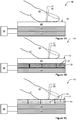
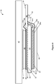
- FIGS 1A-1C show an example of a schematic diagram of an ultrasonic sensor system.
- ultrasonic sensor system 10 includes an ultrasonic transmitter 20 and an ultrasonic receiver 30 under a platen 40.
- the ultrasonic transmitter 20 may be a piezoelectric transmitter that can generate ultrasonic waves 21 (see Figure 1B ).
- the ultrasonic receiver 30 includes a piezoelectric material and an array of pixel circuits disposed on a substrate. In operation, the ultrasonic transmitter 20 generates an ultrasonic wave 21 that travels through the ultrasonic receiver 30 to the exposed surface 42 of the platen 40.
- the ultrasonic energy may be transmitted into, absorbed or scattered by an object 25 that is in contact with the platen 40, such as the skin of a fingerprint ridge 28, or reflected back.
- an object 25 that is in contact with the platen 40, such as the skin of a fingerprint ridge 28, or reflected back.
- Control electronics 50 may be coupled to the ultrasonic transmitter 20 and ultrasonic receiver 30 and may supply timing signals that cause the ultrasonic transmitter 20 to generate one or more ultrasonic waves 21.
- the control electronics 50 may then receive signals from the ultrasonic receiver 30 that are indicative of reflected ultrasonic energy 23.
- the control electronics 50 may use output signals received from the ultrasonic receiver 30 to construct a digital image of the object 25.
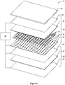
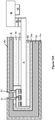
- FIG 2 shows an example of an exploded view of an ultrasonic sensor system 10 including an ultrasonic transmitter 20 and an ultrasonic receiver 30 under a platen 40.
- the ultrasonic transmitter 20 may be a plane wave generator including a substantially planar piezoelectric transmitter layer 22.
- Ultrasonic waves may be generated by applying a voltage to the piezoelectric layer to expand or contract the layer, depending upon the signal applied, thereby generating a plane wave.
- the voltage may be applied to the piezoelectric transmitter layer 22 via a first transmitter electrode 24 and a second transmitter electrode 26.
- an ultrasonic wave may be made by expanding or contracting the piezoelectric transmitter layer 22. This ultrasonic wave may travel towards a finger (or other object to be detected), passing through the platen 40.
- the first and second transmitter electrodes 24 and 26 may be metallized or otherwise conductive electrodes, for example, metal layers that coat opposing sides of the piezoelectric transmitter layer 22.
- the ultrasonic receiver 30 may include an array of pixel circuits 32 disposed on a substrate 34, which also may be referred to as a backplane, and a piezoelectric receiver layer 36 positioned on or otherwise coupled to the underlying pixel circuits 32.
- each pixel circuit 32 may include one or more thin-film transistors and, in some implementations, one or more additional circuit elements such as diodes, capacitors, and the like.
- Each pixel circuit 32 may be configured to convert an electric charge generated by the piezoelectric receiver layer 36 proximate to the pixel circuit into an electrical signal.
- Each pixel circuit 32 may include a pixel input electrode 38 that electrically couples the piezoelectric receiver layer 36 to the pixel circuit 32.
- a receiver bias electrode 39 is disposed on a side of the piezoelectric receiver layer 36 opposite the pixel circuits 32.
- the receiver bias electrode 39 may be grounded or biased to control which signals are passed to a TFT array.
- the receiver bias electrode may include, for example, one or more layers of aluminum, an aluminum alloy, copper, a copper alloy, copper and nickel, gold, platinum and gold, chrome and gold, chrome and aluminum, chrome and copper, chrome with copper and gold, silver, indium-tin-oxide (ITO) or other conductive oxide, silver and urethane polymer, or other suitably conductive material.
- ITO indium-tin-oxide
- Control electronics 50 may be electrically connected with the first transmitter electrode 24 and the second transmitter electrode 26, as well as with the receiver bias electrode 39 and the pixel circuits 32 on the TFT substrate 34.
- the control electronics 50 may operate substantially as discussed previously with respect to Figures 1A-1C .
- the platen 40 can be any appropriate material that can be acoustically coupled to the receiver, with examples including plastic, ceramic, sapphire, composite materials, metal and metal alloys, metal-filled polymers, polycarbonate, and glass.
- the platen 40 can be a cover plate, e.g., a cover glass or a cover lens for a display.
- the platen 40 may be a metal such as aluminum, an aluminum alloy, chrome-molybdenum, stainless steel, or a metal-filled polymer. Detection and imaging can be performed through relatively thick platens if desired, e.g., 1 mm or more.
- a casing or housing for an electronic device may serve as a platen.
- the back, sides or front of a mobile device enclosure may serve as a platen, as the ultrasonic sensor described herein may image fingerprints or acquire biometric information directly through the enclosure wall.
- a coating such as a thin layer of urethane, acrylic, parylene or a diamond-like coating (DLC) may serve as a platen.
- piezoelectric materials examples include piezoelectric polymers having appropriate acoustic properties, for example, an acoustic impedance between about 2.5 MRayls and 5 MRayls.
- piezoelectric materials that may be employed include ferroelectric polymers such as polyvinylidene fluoride (PVDF) and polyvinylidene fluoride-trifluoroethylene (PVDF-TrFE) copolymers.
- PVDF copolymers examples include 60:40 (molar percent) PVDF-TrFE, 70:30 PVDF-TrFE, 80:20 PVDF-TrFE, and 90:10 PVDR-TrFE.
- piezoelectric materials include Teflon® and other PTFE polymers, polyvinylidene chloride (PVDC) homopolymers and copolymers, polytetrafluoroethylene (PTFE) homopolymers and copolymers, and diisopropylammonium bromide (DIPAB).
- PVDC polyvinylidene chloride
- PTFE polytetrafluoroethylene
- DIPAB diisopropylammonium bromide
- each of the piezoelectric transmitter layer 22 and the piezoelectric receiver layer 36 may be selected so as to be suitable for generating and receiving ultrasonic waves.
- a PVDF piezoelectric transmitter layer 22 is approximately 28 ⁇ m thick and a PVDF-TrFE receiver layer 36 is approximately 12 ⁇ m thick.
- Example frequencies of the ultrasonic waves are in the range of 5 MHz to 30 MHz, with wavelengths on the order of a quarter of a millimeter or less.
- Figures 1A through 1C and 2 show example arrangements of ultrasonic transmitters and receivers in an ultrasonic sensor system, with other arrangements possible.
- the ultrasonic sensor system may include an acoustic delay layer.
- an acoustic delay layer can be incorporated into the ultrasonic sensor system 10 between the ultrasonic transmitter 20 and the ultrasonic receiver 30.
- An acoustic delay layer can be employed to adjust the ultrasonic pulse timing, and at the same time electrically insulate the ultrasonic receiver 30 from the ultrasonic transmitter 20.
- the delay layer may have a substantially uniform thickness, with the material used for the delay layer and/or the thickness of the delay layer selected to provide a desired delay in the time for reflected ultrasonic energy to reach the ultrasonic receiver 30. In doing so, the range of time during which an energy pulse that carries information about the object by virtue of having been reflected by the object may be made to arrive at the ultrasonic receiver 30 during a time range when it is unlikely that energy reflected from other parts of the ultrasonic sensor system 10 is arriving at the ultrasonic receiver 30.
- the TFT substrate 34 and/or the platen 40 may serve as an acoustic delay layer.
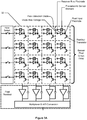
- Figure 3A depicts a 4 x 4 pixel array of pixels for an ultrasonic sensor.
- Each pixel may, for example, be associated with a local region of piezoelectric sensor material, a peak detection diode and a readout transistor; many or all of these elements may be formed on or in the backplane to form the pixel circuit.
- the local region of piezoelectric sensor material of each pixel may transduce received ultrasonic energy into electrical charges.
- the peak detection diode may register the maximum amount of charge detected by the local region of piezoelectric sensor material.
- Each row of the pixel array may then be scanned, e.g., through a row select mechanism, a gate driver, or a shift register, and the readout transistor for each column may be triggered to allow the magnitude of the peak charge for each pixel to be read by additional circuitry, e.g., a multiplexer and an A/D converter.
- the pixel circuit may include one or more TFTs to allow gating, addressing, and resetting of the pixel.
- Each pixel circuit 32 may provide information about a small portion of the object detected by the ultrasonic sensor system 10. While, for convenience of illustration, the example shown in Figure 3A is of a relatively coarse resolution, ultrasonic sensor systems having a resolution on the order of 500 pixels per inch or higher that are configured with a layered structure substantially similar to that shown in Figure 2 have been demonstrated by the present inventors.
- the detection area of the ultrasonic sensor system 10 may be selected depending on the intended object of detection. For example, the detection area may range from 5 mm x 5 mm for a single finger to 3 inches x 3 inches for four fingers. Smaller and larger areas may be used as appropriate for the object.
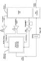
- FIG. 3B shows an example of a high-level block diagram of an ultrasonic sensor system. Many of the elements shown may form part of control electronics 50.
- a sensor controller may include a control unit that is configured to control various aspects of the sensor system, e.g., ultrasonic transmitter timing and excitation waveforms, bias voltages for the ultrasonic receiver and pixel circuitry, pixel addressing, signal filtering and conversion, readout frame rates, and so forth.
- the sensor controller may also include a data processor that receives data from the ultrasonic sensor circuit pixel array. The data processor may translate the digitized data into image data of a fingerprint or format the data for further processing.
- control unit may send a transmitter (Tx) excitation signal to a Tx driver at regular intervals to cause the Tx driver to excite the ultrasonic transmitter and produce planar ultrasonic waves.
- the control unit may send level select input signals through a receiver (Rx) bias driver to bias the receiver bias electrode and allow gating of acoustic signal detection by the pixel circuitry.
- a demultiplexer may be used to turn on and off gate drivers that cause a particular row or column of sensor pixel circuits to provide output signals.
- Output signals from the pixels may be sent through a charge amplifier, a filter such as an RC filter or an anti-aliasing filter, and a digitizer to the data processor. Note that portions of the system may be included on the TFT backplane and other portions may be included in an associated integrated circuit.
- some implementations described herein relate to ultrasonic receivers including piezoelectric receiver layers bonded to TFT arrays with an adhesive. Some implementations relate to processes for forming ultrasonic sensors include bonding a piezoelectric receiver layer to a TFT array.
- bonding refers to the fastening together of two or more solid objects by the use of glue, cement, or other adhesive, and "bonded” to the two or more solid objects so fastened.
- adhesives include one- and two-part epoxies, cyanoacrylates, silicones, polyurethane, thermoplastics, elastomeric adhesives, thermoset adhesives, UV-curable adhesives, hot curing adhesives, hot-melt adhesives, phenolics, acrylics, acrylates, polyamides, contact adhesives and pressure sensitive adhesives (PSAs).
- the term "fingerprint” may refer to a fingerprint or a thumbprint.
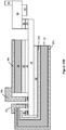
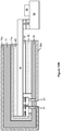
- FIG 4 shows an example of a schematic diagram of an ultrasonic sensor system 10 including a bonded piezoelectric receiver layer 36.
- the ultrasonic sensor system 10 includes a platen 40, a piezoelectric receiver layer 36, a TFT substrate 34, and a piezoelectric transmitter layer 22, as discussed above with reference to Figures 1 and 2 .
- Both sides of the piezoelectric transmitter layer 22 may be metallized or otherwise coated with a conductive material to form a first transmitter electrode 24a, which can be connected to a first transmitter lead 24b, and a second transmitter electrode 26a, which can be connected to second transmitter lead 26b.
- the metallized piezoelectric transmitter film may be bonded to the TFT substrate 34 by an adhesive 68.
- Adhesive 68 and other adhesive layers such as adhesive 62, adhesive 64, and adhesive 66 are enlarged for clarity in Figures 4 and 7A-12B , and like other layers in the Figures are generally not drawn to scale.
- a spacer layer 80 is disposed between the piezoelectric receiver layer 36 and the platen 40.
- the spacer layer 80 may provide clearance for various components of the ultrasonic sensor system 10, including components attached to a flexible printed circuit (FPC) 90.
- Flexible printed circuits may also be known simply as "flex.”
- the FPC 90 may include one or more electrodes or electrical conductors within the FPC 90 or on one or both sides of the FPC 90.
- the spacer layer 80 may not be present in some implementations. If present, the spacer layer 80 may be bonded to the platen 40 via an adhesive 62 and to the metallized side of the piezoelectric receiver layer 36 with an adhesive 64.
- One side of the piezoelectric receiver layer 36 may be metallized to form a receiver bias electrode 39a, which can be connected to a receiver bias electrode lead 39b. According to various implementations, the receiver bias electrode 39a and receiver bias electrode lead 39b may use the same or different materials.
- the other side of piezoelectric receiver layer 36 may be bonded to pixel circuits 32 by an adhesive 66. As discussed above with respect to Figure 2 , each pixel circuit 32 may include a pixel input electrode.
- the piezoelectric receiver layer 36 may be electrically coupled or otherwise connected to the pixel circuits 32 through the pixel input electrodes.
- the piezoelectric receiver layer 36 is capacitively coupled to the pixel circuits 32 through the adhesive 66.
- the piezoelectric receiver layer 36 is resistively coupled to the pixel circuits 32 through, for example, an anisotropically conductive or lightly conductive adhesive 66.
- the TFT substrate 34 may be a thin substrate, e.g., a glass or plastic substrate, on which the pixel circuits 32 are fabricated.
- the TFT substrate 34 may be silicon, single-crystal silicon or other semiconductor material, such as a silicon wafer or a silicon-on-insulator wafer.
- the pixel circuits 32 and other circuitry related to TFT substrate 34 may be formed from transistors fabricated in the substrate, such as a conventional silicon device wafer. An example of pixel circuits 32 are shown in Figure 3A , as discussed above.
- the TFT substrate may have additional components fabricated thereon, such as one or more conductive bond pads 33.
- a protective backside cap 60 may be disposed to protect the elements within such as the piezoelectric transmitter layer 22 from mechanical or environmental damage.
- the protective cap 60 may provide protection for the elements within the cap 60 from electro-magnetic interference (EMI) or devices outside the cap 60 from the EMI generated by the elements within.
- EMI electro-magnetic interference
- the FPC 90 may have one or more passive or active components mounted thereon.
- the first transmitter lead 24b, the second transmitter lead 26b, and the receiver bias electrode lead 39b may be configured to be in electrical communication with one or more of these components via the FPC 90.
- a chip-on-flex (COF)-attached application specific integrated circuit (ASIC) 92 may be disposed on one side or the other of the FPC 90.
- One or more discrete devices such as capacitors, resistors and inductors may be included on one or both sides of FPC 90 (not shown).
- the ultrasonic sensor system 10 may further be configured to connect to a printed circuit board (PCB) or other integration substrate via the FPC 90.
- PCB printed circuit board
- one or more stiffeners 94 may be attached to the FPC 90.
- materials for the leads include conductive inks, copper films, and other conductors.
- wire bonds or braided wire may be employed.
- stiffener materials include both conductive and insulative materials such aluminum, anodized aluminum, stainless steel, printed-circuit board material such as FR4, polyimide materials, and thermoplastics.
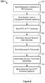
- FIG. 5 is an example of a flow diagram illustrating a manufacturing process for an ultrasonic sensor.
- a TFT substrate is provided.
- the TFT substrate may include pixel circuits formed thereon including conductive pads deposited over the inputs of the pixel circuits to form pixel input electrodes.
- the TFT substrate may also include conductive routing and bond pads to provide connections between the pixel circuits, the ultrasonic receiver, the ultrasonic transmitter, a flexible printed circuit, or other electrical components according to the particular implementation. Standard TFT processing may be employed to form the TFT substrate.
- the TFT substrate may include a borosilicate glass with a thickness between about 300 and 700 microns.
- the glass may be thinned to reduce the overall thickness of the sensor system 10.
- the TFT substrate 34 may include a thin, flexible glass or plastic layer with a thickness less than about 300 microns or less than about 100 microns.
- TFT substrate materials include borosilicate glass and flexible polymeric substrates including polyimide including NeopulimTM transparent polyimide, polyethylene terephthalate (PET), and polyethylene napthalate (PEN).
- a piezoelectric receiver layer is provided.
- the piezoelectric receiver may be provided as piezoelectric layer having single-sided metallization.
- a piezoelectric transmitter (Tx) is provided.
- the piezoelectric transmitter may be provided as a piezoelectric layer having single-sided or double-sided metallization.
- Examples of metallization for either the receiver or transmitter electrode layers include aluminum (Al), an aluminum alloy, copper (Cu), a copper alloy, nickel-copper (NiCu), gold (Au), platinum-gold (PtAu), chrome-gold (CrAu), chrome-aluminum (CrAl), chrome-copper (CrCu), chrome with copper and gold, silver, ITO or other conductive oxide, and silver (Ag) in a polymer matrix such as silver ink, silver epoxy, or polyurethane (AgUr).
- one or more receiver or transmitter electrode layers may be formed from a layer of nickel or chrome between approximately 15 nm and 50 nm thick that is deposited on top of a layer of copper or copper alloy with a thickness between approximately 0.1 ⁇ m and 0.5 ⁇ m.
- a protective coating such as a thin layer of urethane, acrylic, parylene or a diamond-like coating (DLC) may be disposed over the metallization to provide scratch and corrosion resistance.
- a single piezoelectric layer may be provided for both the receiver and the transmitter in wrap-around configurations. Examples of such implementations are discussed below with respect to Figures 12A-13G .
- Blocks 108 and 110 may be optionally performed according to the particular implementation.
- a spacer layer may be provided.
- Example spacer materials include glass substrates such as borosilicate glass, soda lime glass, and GorillaTM glass, and plastic substrates such as polycarbonate.
- Example thicknesses of a spacer layer can range from about 0.1 mm to 1 mm or more.
- a backside protective cap may be provided.
- the backside cap can be a material such as metal-coated plastic or a tin-plated steel.
- Example thicknesses can range from about 50 ⁇ m to 200 ⁇ m or larger.
- one or more FPCs or other electrically connective means may be provided.
- the FPC may have one or more electrical and/or mechanical components attached thereto such as ASICs, resistors, capacitors, and mechanical stiffeners.
- the above-described components may be assembled at block 114 to form an ultrasonic sensor assembly Examples of assembly according to various implementations are discussed further below with respect to Figures 6-13G .
- the sensor assembly can then optionally be calibrated and tested at block 116 prior to bonding to a cover glass or other platen.
- a thin coating such as a layer of urethane, an acrylic coating, parylene, or a DLC may be applied to the outer surface of the piezoelectric receiver layer to serve as a platen and to provide scratch resistance and environmental protection.
- FIG. 6 is another example of a flow diagram illustrating a manufacturing process for an ultrasonic sensor.
- One or more operations in Figure 6 may be performed as part of block 114 of the method 100 described above.
- a piezoelectric receiver layer is bonded to a TFT substrate with an adhesive.
- the adhesive may be relatively thin with a substantially uniform thickness. Bonding the piezoelectric receiver layer can include any appropriate bonding process such as vacuum bonding, hot-roll lamination, cold-roll lamination, contact bonding, hot-press bonding, cold-press bonding, or other adhesive bonding process.
- liquid adhesive application processes include dispensing, micro-dispensing, screen printing, silk-screening, stamping, gravure printing, slot coating, slot die coating, spraying, brushing, dipping, roller or reverse roller application, blade over drum application, wire rod application, and application by inkjet or dip pen.
- the adhesive is selected and bonding performed to avoid acoustic non-uniformities such as air bubbles or large variations in material density, speed of sound, and thickness. Microscopic voids, striations, local delaminations, puckers, blisters, remnant solvents, embedded particles, and material inhomogeneities are to be avoided or mitigated.
- adhesives may include PSAs and epoxies.
- a solvent-based adhesive may be used, where the solvent is substantially exhumed prior to making contact between joined surfaces.
- Joining processes may include laminating, mounting, or mating.
- the adhesive is electrically conductive through its thickness but resistive in the lateral direction.
- adhesives include anisotropic conductive film (ACF).
- ACF anisotropic conductive film
- a thin yet moderately resistive adhesive such as (3-aminopropyl) triethoxysilane (APTES) may be used.
- APTES (3-aminopropyl) triethoxysilane
- Employing such an adhesive may reduce or eliminate capacitive coupling between the piezoelectric receiver layer and the TFT pixel circuits.
- adhesive bonding of the piezoelectric receiver layer to the TFT substrate is chosen to be highly electrically resistive in the lateral direction so as to avoid electrical shorting between adjacent pixel circuits and to maintain the addressability of the TFT pixel.
- the adhesive may have a bulk or volume resistivity of more than about 1 M ⁇ -cm. In some implementations, a resistivity of 1E12 ⁇ -cm or higher may be used.
- Electrically conductive transparent adhesives can be made from formulations of polyfunctional adhesion promoters, chosen such that the functional group chemistry is suitable for a given pair of bonding surfaces.
- a suitable material for use as an electrically conductive transparent adhesive in such implementations is APTES, although other materials may also be used.
- APTES is a liquid at standard temperature and pressure (STP), and may be dissolved in water or acetone in a ratio of about 1 to 50% APTES by volume. In some implementations, the ratio may be about 4% APTES by volume, but ratios larger or smaller than 4% may also be used.
- a layer of APTES may be applied to a surface via any suitable process, including dip coating, spin coating, spray coating, or other dispensing method.
- vapor or vacuum deposition methods may be used.
- surfaces Prior to the application of APTES, surfaces may be cleaned and activated to improve bonding, such as oxygen plasma or ultraviolet ozone (UVO) exposure.
- Adjacent surfaces may be bonded to one another by applying pressure, and the bonding process may be accelerated through the application of heat during the bonding process.
- methods such as hot pressing, hot-roll lamination, or clamping within an oven may be used to provide both pressure and heat.
- application of pressure at a temperature of about 80°C for two hours or more provides sufficient adhesive strength, while at least 24 hours may be used at room temperature (about 25°C).
- block 122 may be performed without modification to standard TFT processing.
- the bonding may be performed without shorting or otherwise damaging the pixel circuits.
- a spacer layer is optionally bonded to the piezoelectric receiver.
- the spacer layer 80 may serve as a standoff that ensures that the receiver bias electrode lead 39b and the FPC 90 do not interfere with mounting the TFT substrate 34 with the piezoelectric receiver layer 36 on the platen 40.
- the spacer layer 80 may also serve as an acoustic delay layer that improves sensor performance.
- Figures 7A and 7B show examples of implementations with and without spacer layers. If employed, a spacer layer may be bonded with an adhesive.
- the adhesive may be relatively thin with a uniform thickness and bonding performed in a manner to avoid acoustic non-uniformities such as air bubbles or large variations in material density or speed of sound.
- adhesives may include pressure sensitive adhesives, epoxies and other suitable adhesives as described above.
- an FPC is optionally bonded to the TFT substrate.
- One or more electrodes on the FPC can be connected to one or more conductive pads on the TFT substrate with an electrically conductive adhesive such as ACF.
- an FPC can be bonded to one or both of the piezoelectric receiver and the piezoelectric transmitter.
- a cooling apparatus such as a Peltier cooler, a refrigerated block cooler, or a suitably large heat sink may be thermally coupled to the piezoelectric receiver layer 36, particularly over the TFT pixel circuits 32.
- the piezoelectric receiver layer 36 (and possibly the piezoelectric transmitter if already attached) may be cooled and retained at a temperature below the Curie temperature of the piezoelectric material.
- One or more FPCs may be bonded to the ultrasonic sensor assembly, such as an FPC for the piezoelectric transmitter, an FPC for the piezoelectric receiver, one or more FPCs for the data and control lines on the TFT substrate, and combinations thereof (e.g. a data flex for transferring data and control signals, and a power flex for transferring power to the piezoelectric transmitter and receiver).
- the FPC may contain wider traces for supplying power to the piezoelectric transmitter or receiver, to minimize ohmic losses along the traces.
- the FPC may have traces and pads that connect to or mate with electrical connectors at one or both ends of the FPC. More than one connector may be included at either end.
- the FPC may have one or more layers of metal, such as on the topside, bottom side and internal to the flex, which may be used for carrying electrical signals.
- the FPC may have vias that allow electrical connections between one or more layers of the FPC.
- the FPC may have a multiplicity of vias to further reduce ohmic losses to the piezoelectric receiver or transmitter by connecting traces on different layers in parallel.
- the FPC may contain slots or cutout regions (e.g. a split flex) to allow one portion of the flex to be attached to an upper surface of a sensor assembly and another portion to a lower surface of the sensor assembly, such as to a piezoelectric receiver layer on the top side of a TFT substrate and a piezoelectric transmitter on the bottom side of the TFT substrate.
- the FPC may contain slots or cutout regions to allow a portion of the flex to be connected to a first connector at one end of the flex and another portion to be connected to a second connector at the same end, for example, to allow electrical connections with an external printed circuit board.
- the FPC may include pads for the attachment of one or more integrated circuits, capacitors, resistors, inductors, or other active or passive components.
- portions of the flex may be wrapped, folded, rolled, or otherwise bent to accommodate connections to the ultrasonic sensor assembly.
- the receiver bias electrode is electrically connected.
- the receiver bias electrode may be connected directly to the FPC or to a conductive pad on the TFT substrate for connection to the FPC.
- block 128 may be performed prior to block 126.
- materials to connect the receiver bias electrode include conductive inks, conductive epoxies, ink-jetted metal and conductive adhesives.
- the FPC may overlay or underlay the TFT substrate, in conjunction with the TFT pixel circuits, and be attached to the receiver bias electrode by hot-press bonding and/or by using a separate adhesive such as ACF.
- the FPC may overlay or underlay the TFT substrate and be attached directly to the piezoelectric receiver layer by hot-press bonding and/or by using a separate adhesive.
- An example of such an implementation is shown in Figure 11A . Temperatures during this attachment can be less than 85°C in some implementations. Additional examples of receiver connections are discussed further below with respect to Figures 10A-10C .
- a piezoelectric transmitter is bonded.
- the piezoelectric transmitter is bonded to the backside (i.e., the side upon which there are no pixel circuits) of the TFT substrate for example, as depicted in Figure 4 .
- the piezoelectric transmitter is bonded to the piezoelectric receiver. Adhesives as discussed above with respect to blocks 122 and 124 may be employed.
- the transmitter electrodes are electrically connected.
- the transmitter electrodes may be connected directly to the FPC or to conductive bond pads on the TFT substrate. Examples of materials include conductive inks, conductive epoxies, conductive adhesives, and solders.
- the FPC may underlay or overlay the TFT substrate, in conjunction with the TFT pixel circuits, and be attached to a transmitter electrode by a conductive adhesive or other bonding method that ensures good electrical conduction between the FPC and transmitter electrodes.
- the FPC may overlay or underlay the TFT substrate, in conjunction with the TFT pixel circuits, and be attached directly to the piezoelectric transmitter layer by hot-press bonding and/or by using a separate adhesive. Temperatures during this attachment can be less than 85°C in some implementations.
- a backside cap is optionally bonded to the TFT substrate.
- the backside cap is sized such that there is an air gap between the transmitter and the backside cap.
- the backside cap mechanically contacts or is bonded to the transmitter or other sensor component.
- portions of the sensor assembly may be potted to form the protective cap, or a cap may be molded around portions of the sensor assembly. At this stage, the ultrasonic sensor may be tested and bonded to a cover glass or other platen as desired.
- a single ultrasonic sensor from a single TFT substrate may be assembled as a single ultrasonic sensor through all steps in the assembly sequence.
- a strip (1 x n) or array (m x n) of TFT substrates may be assembled with appropriately sized and scaled piezoelectric transmitters, piezoelectric receiver layers, spacers, protective caps, adhesives and/or other sensor elements in one or more steps of manufacturing process 100 or process 120.
- Strips, sheets, panels or sub-panels of TFT substrates may be diced, scribed or otherwise separated at various steps in the manufacturing process prior to attaching subsequent elements of the ultrasonic sensor assembly. Steps such as dispensing, curing and other assembly process sequences may done serially, in parallel or quasi-continuously such as in a conveyor-belt manner. For example, a curing step for ACF or a conductive epoxy may transpire at the same time and temperature as a curing step for a thermally curing adhesive layer. Liners may be included on top of PSAs that may be removed immediately prior to bonding or lamination to protect the PSA from dust and other particles.
- roll-to-roll, roll-to-glass sheet, pick-and-place, or tape-and-reel processing may be used for one or more assembly steps.
- individual piezoelectric receiver layers or transmitters may be picked and placed onto TFT substrates or vice versa, or a sheet of m x n receivers may be picked or roll laminated onto a glass sheet of m x n TFT substrates.
- modifications to the processes shown may be implemented without departing from the scope of the disclosure. For example, it will be understood from the examples of Figures 7A-13G , below, that various other operations that are not depicted can be incorporated in the example processes that are schematically illustrated.
- one or more additional operations can be performed before, after, simultaneously, or between any of the illustrated operations.
- all illustrated operations may not be performed in some implementations. It should also be understood that other elements may be included and/or certain illustrated elements omitted in the schematic diagrams below.
- Figures 7A-13G show examples of schematic diagrams of various components of an ultrasonic sensor. The examples in these Figures provide additional detail and alternative implementations to the ultrasonic sensor described above with respect to Figure 4 .
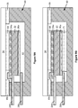
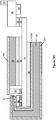
- Figures 7A and 7B show examples of ultrasonic receivers with and without spacer layers disposed between the ultrasonic receiver and a platen.
- a piezoelectric receiver layer 36 is shown bonded to a TFT substrate 34 by an adhesive 66.
- the pixel circuits 32 are shown as an intermediate layer between the TFT substrate 34 and the piezoelectric receiver layer 36, the adhesive 66 may contact the pixel input electrodes of the pixel circuits 32, as well as the surface of the TFT substrate 34 in areas between the pixel circuits 32.
- FIGS 7A and 7B Also shown in Figures 7A and 7B are an FPC 90, having an ASIC 92 and a stiffener 94 attached thereto and electrically connected to the pixel circuits 32 by an ACF 96 bonded to a TFT array conductive bond pad 33d, and a receiver bias electrode 39a connected to a receiver bond pad 33c by a receiver bias electrode lead 39b, which may be, for example, a metal wire, a bond wire, a metal trace, or a conductive adhesive material such as silver epoxy or silver ink.
- connection between the receiver bias electrode 39a and the receiver conductive bond pad 33d may be formed in one of several ways such as dispensing, stamping, metal evaporation with a shadow mask, sputtering and photolithographic masking, or ink-jetting. Other conductive leads, traces and vias may be formed in a similar manner.
- Figure 7A includes a spacer layer 80, bonded to the receiver bias electrode 39a by an adhesive 64 and to a platen 40 by an adhesive 62.
- no spacer layer is present, with the receiver bias electrode 39a bonded directly to the platen 40 by the adhesive 64. Examples of adhesives are described further below.
- spacer layer thicknesses range from about 0.1 mm to about 0.5 mm; examples of adhesive thicknesses range from about 0.001 mm to about 0.25 mm. In implementations that do not employ a spacer layer, the thickness of the adhesive 64 may be at the high end of this range to provide space for components attached to the FPC 90.
- an ultrasonic transmitter (not depicted) may be below the TFT substrate 34 as described above with respect to Figure 4 .
- Various aspects of the arrangements shown in Figures 7A and 7B may also be implemented with an ultrasonic transmitter positioned between the TFT substrate 34 and the platen 40, including the use of a spacer layer 80 disposed between the ultrasonic transmitter and the platen 40.
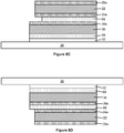
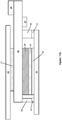
- FIGs 8A-8D show examples of arrangements of an ultrasonic transmitter and an ultrasonic receiver of an ultrasonic sensor.
- the Figures are oriented such that a platen or cover glass would be positioned above each stack.
- the TFT substrate 34 may serve as the platen.
- the ultrasonic receiver including a piezoelectric receiver layer 36, a receiver bias electrode 39a, and pixel circuits 32, is positioned above a TFT substrate 34, with the ultrasonic transmitter, including piezoelectric transmitter layer 22 and first and second transmitter electrodes 24a and 26a, positioned below the TFT substrate 34.
- the ultrasonic transmitter including the piezoelectric transmitter layer 22 and the first and second transmitter electrodes 24a and 26a is positioned above the TFT substrate 34, with the ultrasonic receiver, including the piezoelectric receiver layer 36, the receiver bias electrode 39a, and the pixel circuits 32, positioned below the TFT substrate 34.
- Figure 8C shows an example of an implementation in which both the ultrasonic transmitter and the ultrasonic receiver are above the TFT substrate 34.
- the ultrasonic transmitter including the piezoelectric transmitter layer 22 and the first and second transmitter electrodes 24a and 26a, is positioned above the ultrasonic receiver, with the ultrasonic transmitter bonded to the receiver bias electrode 39a of the ultrasonic receiver.
- the ultrasonic receiver is bonded to the TFT substrate 34, with the piezoelectric receiver layer 36 electrically coupled to the pixel circuits 32.
- FIG 8D shows an example of an implementation in which both the ultrasonic transmitter and the ultrasonic receiver are positioned below the TFT substrate 34.
- the ultrasonic transmitter including the piezoelectric transmitter layer 22 and the first and second transmitter electrodes 24a and 26a, is positioned below the ultrasonic receiver, with the ultrasonic transmitter bonded to the receiver bias electrode 39a of the ultrasonic receiver.
- the ultrasonic receiver is bonded to the TFT substrate 34, with the piezoelectric receiver layer 36 electrically coupled to the pixel circuits 32.
- the side of TFT substrate 34 opposite the pixel circuits 32 may serve as the platen, and may optionally include one or more coatings.
- the side of TFT substrate 34 opposite the pixel circuits 32 may be attached to a separate platen such as a cover glass, or a wall of a mobile device enclosure.
- the ultrasonic transmitter is bonded to the TFT substrate 34 with an adhesive 68, with the first transmitter electrode 24a of the ultrasonic transmitter bonded to the TFT substrate 34.
- the ultrasonic transmitter is bonded to the ultrasonic receiver with an adhesive 69, with the first transmitter electrode 24a bonded to the receiver bias electrode 39a.
- adhesives 68 and 69 include pressure sensitive adhesives, epoxies, and other adhesives as described above.
- the piezoelectric receiver layer 36 may be bonded to the TFT substrate 34 by an adhesive 66 as described above.
- a backside cap may be optionally bonded to the TFT substrate.
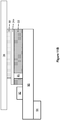
- FIGs 9A and 9B show examples of ultrasonic sensors including backside protective caps 60.
- the backside cap 60 may include a metal, a metal coating or a conductive material sufficient to reduce electromagnetic interference (EMI) and improve acoustic performance.
- Example thicknesses of the backside cap 60 range from about 50 ⁇ m to about 500 ⁇ m.
- the backside cap 60 is separated from the ultrasonic transmitter by an air gap 61.
- the air gap may be about 25 ⁇ m to 100 ⁇ m thick in some implementations.
- the air gap may provide mechanical isolation to prevent potential damage during assembly and to prevent incidental shorting of the transmitter electrode 26a.
- a piezoelectric receiver layer 36 may be attached to TFT pixel circuits 32 (not shown) on TFT substrate 34 opposite the piezoelectric transmitter layer 22.
- the backside cap 60 is bonded directly to the second transmitter electrode 26a by an adhesive layer 71.
- the backside cap 60 can also be bonded to the TFT substrate 34 by an adhesive layer 65.
- adhesives that can be used to bond the backside cap include pressure sensitive adhesives and epoxies having cohesive strength to provide strong, reliable adhesion to the TFT substrate 34.
- first and second transmitter leads 24b and 26b may be routed through, under, or over adhesive layer 65, or through electrically insulated passages through the backside cap 60.
- an acoustic backing layer (not shown) may be applied to the outer side of the transmitter or positioned between the transmitter and the backside cap 60.
- the backing layer may be made, for example, of acoustically absorptive material to absorb emitted ultrasonic energy from the backside of the transmitter and avoid undue reflections back towards the platen or cover glass.
- the backing layer may include an open-cell or closed-cell foam or foam adhesive, exhibiting a relatively small acoustic impedance relative to the piezoelectric transmitter so as to avoid undue loss of acoustic energy into the backing layer.
- a piezoelectric receiver layer 36 may be attached to TFT pixel circuits 32 (not shown) on TFT substrate 34 opposite the piezoelectric transmitter layer 22.
- Figure 9C shows an example in which the backside cap 60 forms a frame that snugly wraps around the TFT substrate 34.
- the backside cap 60 may be a molded component including a support portion 60A to support the TFT substrate 34.
- the support portion 60A may be or include an adhesive to the backside cap 60.
- One or more conductive leads 37 from an underlying transmitter and/or receiver may be routed between the backside cap 60 and the TFT substrate 34 to an FPC 90.
- the one or more conductive leads 37 may be integrated into the backside cap 60.
- the backside cap 60 may be metallized, e.g., with copper tape, a metal foil, or a metal coating on one or both sides of the cap.
- the FPC 90 may extend over the backside cap to be further connected via flex-on-glass (FOG) pads 35, which may include ACF, to electrically couple to a transmitter and/or receiver.
- FOG flex-on-glass
- the transmitter and/or receiver may be connected to a COF-attached ASIC 92 disposed on the FPC 90.
- a stiffener 94 on the FPC 90 is also depicted in Figure 9C .
- the first and second transmitter electrodes and receiver bias electrodes may be electrically connected in various manners. As discussed above, wire bonds, conductive adhesives, and conductive inks may be used in some implementations.
- Figures 10A-10C show further examples of electrical connections of transmitter and receiver electrodes.
- a piezoelectric receiver layer 36 is metallized with a receiver bias electrode 39a, bonded to a TFT substrate 34 via an adhesive 66 and electrically coupled to TFT pixel circuits 32 on the TFT substrate 34, as described above.
- An ultrasonic transmitter including a metallized piezoelectric transmitter layer 22, is bonded to the opposite side of the TFT substrate 34 by an adhesive 68, as also described above.
- both the receiver and transmitter electrodes are electrically connected at the front (receiver) side of the TFT substrate 34.
- a metallized piezoelectric transmitter layer 22 is wrapped around a TFT substrate 34 to connect to its front surface.
- the TFT substrate 34 includes first and second transmitter bond pads 33a and 33b for connecting the electrodes to conductive routing (not shown) on the TFT substrate 34.
- the conductive routing provides an electrical connection to an FPC 90 via a FOG pad 35 and an ACF 96 overlying the FOG pad 35.
- the first transmitter electrode 24a contacts an ACF 96 overlying the first transmitter bond pad 33a.
- a conductive via 81 can extend through the piezoelectric transmitter layer 22 to electrically connect the second transmitter electrode 26a to the ACF 96, which also overlies the second transmitter bond pad 33b.
- the conductive via 81 may be filled with conductive material or may have sidewalls coated with a conductive material.
- a receiver bias electrode lead 39b can be a conductive adhesive material such as silver epoxy or silver ink, for example, that can be dispensed, screen printed, or ink-jet printed to connect a receiver bias electrode 39a to a receiver bond pad 33c.
- receiver bias electrode lead 39b may include one or more wires or traces that extend from receiver bias electrode 39a forming a separation from the piezoelectric receiver layer 36 (as shown), in some implementations a portion of the receiver bias electrode lead 39b may traverse or flow along a side of the receiver bias electrode 39a and/or along a side of the piezoelectric receiver layer 36 (not shown). In some implementations, the receiver bias electrode lead 39b may connect to a portion of the side of receiver bias electrode 39a, with little or none of the receiver bias electrode lead 39b extending over the top surface of receiver bias electrode 39a.
- the receiver bias electrode lead 39b may include or consist of a filled, partially filled, or unfilled via through the piezoelectric receiver layer 36 in a manner similar to the conductive via 81 described above.
- the conductive vias 81 may be circular, square, rectangular, or other suitable shape.
- receiver bias electrode lead 39b may be formed on the side of or through one or more slits, slots, holes, partial holes, or cutouts in the piezoelectric receiver layer 36.
- a portion of a conductive trace above or below the piezoelectric receiver layer 36 may extend beyond the layer 36 and be connected to the TFT substrate 34 or FPC 90.
- a portion of a conductive trace on the top or bottom of the FPC 90 may be connected to the receiver bias electrode layer 39a using a conductive epoxy, silver-urethane ink or other conductive material, with or without an underlying trace or bond pad on the TFT substrate 34.
- a conductive epoxy or other suitably conductive material may be used to connect patterns or traces on the piezoelectric receiver layer 36 to an underlying trace or pad on the TFT substrate 34.
- Conductive routing on the TFT substrate 34 can connect the receiver bond pad 33c to the FPC 90 via the FOG pad 35 and the ACF 96 overlying the FOG pad 35. In this manner, the transmitter and/or receiver may be connected to a COF-attached ASIC 92 disposed on the FPC 90.
- a stiffener 94 on the FPC 90 is also depicted in Figure 10A .
- the receiver bias electrode lead 39b may flow between the receiver bias electrode lead 39b and traces and/or vias in the FPC 90, augmented by electrical traces and/or pads on the TFT substrate 34.
- the receiver bias electrode lead 39b may flow to connect the receiver bias electrode 39a directly to electrical traces and/or vias in the FPC 90, thereby simplifying the electrical circuit and circumventing the need for a receiver bond pad 33c.
- transmitter bond pads 33a and 33b and receiver bond pad 33c are shown opposite FOG pad 35 on TFT substrate 34 in Figure 10A , it is understood that one or more transmitter or receiver bond pads 33a-33c may be positioned elsewhere on TFT substrate 34, such as near FPC 90. Note that the techniques described for making electrical connections to the receiver bias electrode 39a may also be used for connections to the transmitter electrodes 24a and/or 26a here and elsewhere.
- the metallized piezoelectric transmitter layer 22 is wrapped around the TFT substrate 34 to connect to its front surface.
- the first transmitter electrode 24a contacts an ACF 96 overlying the first transmitter bond pad 33a, as in Figure 10A .
- the second transmitter electrode 26a may be connected to the second transmitter bond pad 33b by a conductive adhesive 83 such as silver epoxy or silver ink.
- the conductive adhesive 83 can be dispensed or ink-jet printed, for example.
- all connections from the transmitter and receiver bond pads 33a, 33b, and 33c may be made with ACF 96, with the second transmitter electrode 26a connected to the ACF 96 through a conductive via 81 as in Figure 10A .
- an FPC may overlay or underlay an ultrasonic transmitter or receiver.
- an electrode of the FPC may be in direct electrical communication with the metallized electrode of a piezoelectric layer or with the piezoelectric layer itself.
- Figures 11A and 11B show examples of implementations in which an electrode of a flexible printed circuit is in direct electrical communication with a piezoelectric layer of an ultrasonic sensor.
- an electrode in the FPC may be separated from the piezoelectric layer by a thin insulating layer. For example, an insulating layer of 0.1 ⁇ m to 20 ⁇ m between an electrode in the FPC and the piezoelectric layer would permit electrical communication between the two.
- FIG 11A shows the FPC 90 overlaying a piezoelectric receiver layer 36, which is bonded to a TFT substrate 34 via an adhesive 66 and electrically coupled to TFT pixel circuits 32.
- the piezoelectric receiver layer 36 is not metallized.
- the FPC 90 is bonded to a platen 40 by an adhesive 73.
- the FPC 90 may overlay and be attached to the piezoelectric receiver layer 36 by hot-press bonding and/or by using a separate adhesive. Temperatures during this attachment can be less than 85°C in some implementations.
- the FPC 90 may be connected to conductive bond pads 33 on a TFT substrate 34 by ACF 96 or other appropriate conductive material.
- connections to the FPC 90 can be made from the ultrasonic transmitter and/or other sensor components as described above. In this manner, connections can be made to a COF-attached ASIC 92 disposed on the FPC 90.
- a stiffener 94 on the FPC 90 is also depicted in Figure 11A .
- an ultrasonic transmitter 20 (not shown) may be attached to the TFT substrate 34 on a side opposite TFT pixel circuits 32.
- an FPC 90 is directly attached to a piezoelectric transmitter layer 22.
- the FPC 90 is attached to the piezoelectric transmitter layer 22 by hot-press bonding and/or by using a separate adhesive. Temperatures during this attachment can be less than 85°C in some implementations.
- a piezoelectric transmitter layer 22 is metallized on one side with a first transmitter electrode 24a, which can connect to the FPC 90 through a conductive via 81, and be bonded to a TFT substrate 34 by an adhesive 68.
- a second transmitter electrode (not shown) of the ultrasonic transmitter is an electrode within or upon the FPC 90.
- two FPCs may be employed, one bonded to the piezoelectric transmitter layer 22 as shown, and another bonded to the TFT substrate or to the piezoelectric receiver layer as described above.
- a piezoelectric receiver layer 36 may be attached to TFT pixel circuits 32 (not shown) on TFT substrate 34 opposite the piezoelectric transmitter layer 22.
- a piezoelectric layer may be wrapped around the TFT substrate to form both a piezoelectric transmitter layer 22 and a piezoelectric receiver layer 36.
- Figures 12A-12C show examples of ultrasonic sensors in which the same piezoelectric layer is used for both the receiver and the transmitter in wrap-around configurations.
- FIG 12A shows an example in which the TFT substrate 34 is oriented such that its top surface with TFT pixel circuits 32 is configured to face an overlying platen (not shown).
- the piezoelectric transmitter layer 22 and the piezoelectric receiver layer 36 are formed from a single piezoelectric layer, with the piezoelectric receiver layer 36 above the TFT substrate 34 and the piezoelectric transmitter layer 22 below the TFT substrate 34.
- the piezoelectric receiver layer 36 is electrically coupled to TFT pixel circuits 32 and bonded to the TFT substrate 34 by an adhesive 66.
- the piezoelectric transmitter layer 22 is metallized and bonded to the TFT substrate 34 by an adhesive 68.
- An ACF 96 overlies first and second transmitter bond pads 33a and 33b and a receiver bond pad 33c on the TFT substrate 34 to electrically connect to the first and second transmitter electrodes 24a and 26a and the receiver bias electrode 39a.
- Conductive vias 81 may connect the second transmitter electrode 26a and the receiver bias electrode 39a to the ACF.
- Conductive routing on the TFT substrate 34 can connect the bond pads 33a, 33b, and 33c to an ASIC 92 on FPC 90 via a FOG pad 35 and an ACF 96 that overlies FOG pad 35.
- Figure 12B shows an example in which the TFT substrate is oriented such that the TFT pixel circuits 32 and the piezoelectric receiver layer 36 are below the TFT substrate 34 and the piezoelectric transmitter layer 22 is above the TFT substrate 34.
- An ACF 96 covers first and second transmitter bond pads 33a and 33b and a receiver bond pad 33c on the TFT substrate 34 to electrically connect to the first and second transmitter electrodes 24a and 26a and the receiver bias electrode 39a.
- Conductive vias 81 may connect the second transmitter electrode 26a and the receiver bias electrode 39a to the ACF.
- Conductive routing on the TFT substrate 34 can connect the bond pads 33a, 33b, and 33c to an ASIC 92 on FPC 90 via a FOG pad 35 and an ACF 96 that overlies FOG pad 35.
- a platen 40 (not shown) may be attached to the piezoelectric transmitter layer 22.
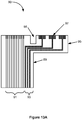
- Figure 12C shows an example of metallization of a PVDF piezoelectric layer to form a piezoelectric transmitter layer and a piezoelectric receiver layer.
- the example in Figure 12C corresponds to a receiver on bottom and transmitter on top configuration.
- the piezoelectric layer 72 may include cutouts 70 to facilitate bending and forming.
- Figure 12C depicts top and bottom views of the unfolded and folded metallized piezoelectric layer 72.
- metallization is nickel (Ni) on copper (Cu), though any appropriate metallization or conductive material including metal-impregnated polymers such as silver-urethane or silver ink may be used.
- Conductive routing and bond pads 43b and 43c, connected to the second transmitter electrode 26a and the receiver bias electrode 39a, respectively, are also shown.
- a bottom view of the unfolded metallized piezoelectric layer 72 is shown, with the piezoelectric layer 72 metallized to form receiver sense electrode 41 a and a first transmitter electrode 24a. In some implementations, the receiver sense electrode 41 a and related bond pad 43d are not formed.
- the first receiver sense electrode 41a includes an anisotropic conductive film such as ACF, an anisotropic conductive polymer, or a thin and lightly conductive layer such as APTES.
- receiver sense electrode 41 a includes a patterned array of electrically isolated electrodes with a size and pitch that mates with underlying pixel input electrodes 38 of TFT pixel circuits 32.
- Conductive routing and bonds pads 43a and 43d, connected to the first transmitter electrode 24a and the receiver sense electrode 41a, respectively, are also shown.
- a top view of the folded piezoelectric layer 72 is shown at 130, with the receiver bias electrode 39a visible and the fold 75 indicated in the Figure. The bond pads 43a-43d are also shown.
- a bottom view of the folded piezoelectric layer 70 is shown with the second transmitter electrode 26a visible.
- the folded views 130 and 140 show electrical traces on top of and through the folded metallized piezoelectric layer 72, as in some implementations the piezoelectric layer 72 is substantially optically transparent.
- FIGS 12A-12C offer low variation between the thickness of the piezoelectric transmitter layer and the thickness of the piezoelectric receiver layer, may allow the transmitter and receiver to be self-aligned, and allow a single-sided adhesive to be applied to bond a folded piezoelectric transmitter and receiver layer to the top and bottom of a TFT substrate.
- thin metal electrodes may be employed with thicker metal traces (e.g., silver ink).
- Adhesives 62, 64, 65, 66, 68, 69, 71, and 73 shown above in these Figures can bond metal to glass or plastic (e.g., a metal electrode to a TFT substrate, a spacer or a platen), metal to metal (e.g., a metal electrode to a metal electrode or cap), glass or plastic to glass or plastic (e.g., a glass or plastic spacer to a glass or plastic platen), or a flexible printed circuit to any of these materials.
- metal to glass or plastic e.g., a metal electrode to a TFT substrate, a spacer or a platen
- metal to metal e.g., a metal electrode to a metal electrode or cap
- glass or plastic to glass or plastic e.g., a glass or plastic spacer to a glass or plastic platen
- a flexible printed circuit to any of these materials.
- adhesives examples include pressure sensitive adhesives and epoxies.
- adhesive layers disposed between the ultrasonic transmitter and/or ultrasonic receiver and the platen may be relatively thin, e.g., less than about 25 ⁇ m or less than about 10 ⁇ m to minimize acoustic reflection and absorption.
- the adhesive thickness may be less than about 5 ⁇ m or less than about 2 ⁇ m.
- the adhesive layer such as a PSA may have a removable liner on one or both sides prior to assembly.
- the adhesive may include a central backing layer with thin adhesive layers on each side of the backing layer, with one or more removable liners optionally attached to the outer surfaces of one or both adhesive layers prior to assembly.
- the adhesives may have a substantially uniform thickness for uniform acoustic reflections and absorption.
- the thickness may vary by no more than +/- 2 ⁇ m. Bonding is performed and the adhesive is selected to prevent formation of acoustic non-uniformities such as air bubbles or large variations in material density, thickness and speed of sound.
- Adhesive 66 bonds the piezoelectric receiver layer to the TFT substrate, and may have the same properties as described above with respect to adhesives 62, 64, 65, 68, 69, 71, and 73.
- vertically electrically conductive adhesives such as ACF and highly resistive (lightly conductive) adhesives such as APTES may be employed.
- the adhesive may have a lateral resistance of at least about 6 M ⁇ -cm, or at least about 10 M ⁇ -cm.
- the adhesive may be lightly conductive with a resistivity larger than about 1 M ⁇ -cm.
- Adhesive 65 can bond the metal backside cap to the TFT substrate. As such, it has high cohesive strength and provides reliable adhesion to the TFT substrate. Examples include pressure sensitive adhesives and epoxies. The same material may also be used for adhesive 71 that bonds the metal cap to the ultrasonic transmitter, in some implementations. These bonds may be coated with one or more protective layers to reduce the ingress of moisture into the layers of the sensor.
- FIG. 13A shows an example of a schematic illustration of a flexible printed circuit configured to wrap around a TFT substrate.
- An FPC 90 may include a flexible cable 89 having control and data traces 91 and low-resistance piezoelectric transmitter and receiver traces 93 printed or otherwise formed thereon.
- the flexible cable 89 may include a wrap-around portion 95 on which the transmitter and receiver traces 93 connect to transmitter and receiver bond pads 97.
- a notch 98 or other feature may be included in the flexible cable 89 to separate the wrap-around portion 95 from the remainder of the flexible cable 89.
- the notch 98 may allow the flexible cable 89 to be more readily wrapped around a portion of a TFT substrate, avoid covering components or alignment marks, or to aid in alignment.
- one or more slits, slots or holes may serve as vias that are traversed or filled in with dispensed or otherwise applied conductive material, allowing electrical connections to be formed between one side of the flexible cable to another side or layer, or to an underlying substrate.
- a flexible printed circuit such as the FPC 90 in Figure 13A may be attached to a TFT substrate that is part of a strip of TFT substrates during an assembly process.
- Figures 13B-13G show examples of schematic illustrations of various stages of a process for attaching flexible printed circuits to thin film transistor sensor arrays.
- Figure 13B shows an example of a strip 44 of TFT substrates 34a-34d.
- Each TFT substrate 34a-34d includes a central area 87 including an array of pixel circuits, one or more peripheral areas 99 for gate drivers, data storage, multiplexers, and additional circuitry as described above with reference to Figures 3A and 3B , and one or more FOG pads 35 for connecting to an FPC.
- the strip 44 is configured to be scribed in scribe regions 86 for singulating the TFT substrates 34a-34d.
- an FPC can be attached to each TFT substrate 34a-34d.
- Figure 13C shows an example of an FPC 90d attached to the TFT substrate 34d by ACF 96.
- a notch 98 in the FPC 90d is aligned with an edge of the TFT substrate 34d.
- the ACF 96 is not shown in Figure 13C , though it is disposed between the FOG pads 35 of the TFT substrate 34d (shown in Figure 13B ) and the FPC 90d.
- the ACF 96 physically connects the FPC 90d to the TFT substrate 34d, and may electrically connect control and data traces 91 of the FPC 90d to the FOG 35 of the TFT substrate 34d.
- the FPC 90d also includes a wrap-around portion 95 with transmitter and receiver bond pads 97 printed thereon.
- the wrap-around portion 95 is configured to wrap around to the opposite side of the TFT substrate 34d, with the transmitter and receiver bond pads 97 configured to connect to the TFT substrate 34d on that side.
- the transmitter and receiver bond pads 97 may connect to a backside-mounted transmitter or to the leads from a transmitter and receiver pair.
- the assembly process can further involve attachment of FPCs to each of the TFT substrates 34a-34d in the strip 44 prior to singulation and wrap-around.
- Figure 13D shows an example of an FPC 90c attached to FOG pads 35 of TFT substrate 34c by ACF 96 (not shown for clarity).
- a wrap-around portion 95 of the FPC 90c overlies but is not connected to the FPC 90d.
- a notch 98 in FPC 90c is aligned with the scribe region 86 that is between the TFT substrate 34c and the TFT substrate 34d. In this manner, the FPC 90c does not cover or obscure the scribe region 86.
- FIG. 13E shows an example of singulation of the TFT substrates 34a-34d.
- Each TFT substrate 34a-34d is shown attached to an FPC 90a-90d, with attachment performed as described above with respect to Figures 13C and 13D .
- Scribing is performed in the scribe regions 86 between each of TFT substrates 34a and 34b, TFT substrates 34b and 34c, and TFT substrates 34c and 34d as indicated by the dashed lines. Because the FPCs 90a-90d do not overlie any of the scribed regions 86, scribing does not involve cutting an FPC.
- Figure 13F shows an example of a singulated TFT substrate 34 attached to an FPC 90 prior to wrapping a wrap-around portion 95 of the FPC 90 around the TFT substrate 34.
- Figure 13G shows an example of the singulated TFT substrate 34 in Figure 13E with the wrap-around portion 95 wrapped around the TFT substrate 34.
- the wrap-around portion may then be physically and/or electrically connected to the TFT substrate 34.
- the example assembly process illustrated in Figures 13B-13G can be performed, for example, as part of block 114 of Figure 5 or block 126 of Figure 6 .
- a portion of FPC 90 may be attached to the top side (circuit side) of TFT substrate 34 and another portion attached to the backside of TFT substrate 34, with a portion of the FPC 90 wrapping loosely or tightly around an edge of the TFT substrate 34. Another portion of the FPC 90 may extend away from the TFT substrate 34 for external electrical connections.
- the FPC 90 may have one or more active or passive components attached thereto, with the components positioned at one or more places along the FPC 90 including the portion near the top side of TFT substrate 34, the wrapped portion, the portion attached to the backside of TFT substrate 34, or the portion of FPC 90 extending away from the ultrasonic sensor assembly.
- Stiffeners may be added to FPC 90 at strategic locations, such as behind the ultrasonic transmitter layer or near connectors. Standoffs may be included on the FPC 90 to control the spacing between the FPC 90 and the piezoelectric transmitter. As noted above, FPC 90 may be single or multi-layer to accommodate the active components, passive components, and connectors.
- a module for vacuum bonding may include a vacuum chamber and gas inlets, outlets, pumps for establishing and maintaining a vacuum, a pressure plate or diaphragm and a shelf that may function as an anvil, and a heater for controlling temperature.
- a module for lamination may include a movable press, gas inlets, outlets, a rotating cylinder for feeding the parts to be laminated at a controlled feed rate, air pressure cylinders for applying pressure to the rotating cylinder, and a heater for controlling temperature.
- a module for dispensing may include a dispenser and one or more sensors for detecting alignment, a controllable X-Y stage, a syringe, and an air pressure cylinder or positive displacement mechanism attached to the syringe.
- a controller may include one or more memory devices and one or more processors configured to execute the program instructions so that the apparatus can perform a method in accordance with the disclosed implementations.
- the processor may include a central processing unit (CPU) or a computer, analog and/or digital input/output connections, motor controller boards, and other like components.
- Program instructions for implementing appropriate process operations may be executed on or by the processor. These program instructions may be stored on the memory devices or other machine-readable media associated with the controller or they may be provided over a network.
- the controller may control all, most, or a subset of the operations of an apparatus.
- the controller may control all or most the operations of an associated with dispensing of a conductive ink or laminating an adhesive.
- the controller may execute system control software including sets of instructions for controlling the timing of the process operations, pressure levels, temperature levels and other parameters of particular manufacturing processes further described with respect to Figures 5 and 6 .
- other computer programs, scripts, or routines stored on memory devices associated with the controller may be employed.
- a user interface may be associated with the controller.
- the user interface may include a display screen, graphical software to display process conditions, and user input devices such as pointing devices, keyboards, touch screens, microphones, and other like components.
- the program instructions for controlling the operations of an apparatus may include computer program code written in any conventional computer readable programming language, such as, for example, assembly language, C, C++, Pascal, Fortran, or others.
- Compiled object code or script may be executed by the processor of the controller to perform the tasks identified in the program instructions.
- signals for monitoring a manufacturing process may be provided by analog and/or digital input connections of the controller.
- Signals for controlling a manufacturing process may be output on analog and/or digital output connections of the controller.
- the hardware and data processing apparatus used to implement the various illustrative logics, logical blocks, modules and circuits described in connection with the aspects disclosed herein may be implemented or performed with a general purpose single- or multi-chip processor, a digital signal processor (DSP), an application specific integrated circuit (ASIC), a field programmable gate array (FPGA) or other programmable logic device, discrete gate or transistor logic, discrete hardware components, or any combination thereof designed to perform the functions described herein.
- a general purpose processor may be a microprocessor, or, any conventional processor, controller, microcontroller, or state machine.
- a processor also may be implemented as a combination of computing devices, such as a combination of a DSP and a microprocessor, a plurality of microprocessors, one or more microprocessors in conjunction with a DSP core, or any other such configuration. In some implementations, particular steps and methods may be performed by circuitry that is specific to a given function.
- the functions described may be implemented in hardware, digital electronic circuitry, computer software, firmware, including the structures disclosed in this specification and their structural equivalents thereof, or in any combination thereof. Implementations of the subject matter described in this specification also can be implemented as one or more computer programs, i.e., one or more modules of computer program instructions, encoded on a computer storage media for execution by or to control the operation of apparatus.
- Computer-readable media includes both computer storage media and communication media including any medium that can be enabled to transfer a computer program from one place to another.
- a storage media may be any available media that may be accessed by a computer.
- such computer-readable media may include RAM, ROM, EEPROM, CD-ROM or other optical disk storage, magnetic disk storage or other magnetic storage devices, or any other medium that may be used to store desired program code in the form of instructions or data structures and that may be accessed by a computer.
- Disk and disc includes compact disc (CD), laser disc, optical disc, digital versatile disc (DVD), floppy disk, and blue-ray disc where disks usually reproduce data magnetically, while discs reproduce data optically with lasers. Combinations of the above also may be included within the scope of computer-readable media. Additionally, the operations of a method or algorithm may reside as one or any combination or set of codes and instructions on a machine readable medium and computer-readable medium, which may be incorporated into a computer program product.
Landscapes
- Engineering & Computer Science (AREA)
- Physics & Mathematics (AREA)
- General Physics & Mathematics (AREA)
- Human Computer Interaction (AREA)
- Multimedia (AREA)
- Theoretical Computer Science (AREA)
- Chemical & Material Sciences (AREA)
- Life Sciences & Earth Sciences (AREA)
- Health & Medical Sciences (AREA)
- Analytical Chemistry (AREA)
- Biochemistry (AREA)
- General Health & Medical Sciences (AREA)
- Immunology (AREA)
- Pathology (AREA)
- Manufacturing & Machinery (AREA)
- Transducers For Ultrasonic Waves (AREA)
- Thin Film Transistor (AREA)
- Investigating Or Analyzing Materials By The Use Of Ultrasonic Waves (AREA)
Applications Claiming Priority (3)
| Application Number | Priority Date | Filing Date | Title |
|---|---|---|---|
| US201361830615P | 2013-06-03 | 2013-06-03 | |
| US14/293,841 US10036734B2 (en) | 2013-06-03 | 2014-06-02 | Ultrasonic sensor with bonded piezoelectric layer |
| PCT/US2014/040746 WO2014197504A1 (en) | 2013-06-03 | 2014-06-03 | Ultrasonic sensor with bonded piezoelectric layer |
Publications (2)
| Publication Number | Publication Date |
|---|---|
| EP3005227A1 EP3005227A1 (en) | 2016-04-13 |
| EP3005227B1 true EP3005227B1 (en) | 2017-04-19 |
Family
ID=51983611
Family Applications (1)
| Application Number | Title | Priority Date | Filing Date |
|---|---|---|---|
| EP14734349.5A Active EP3005227B1 (en) | 2013-06-03 | 2014-06-03 | Ultrasonic sensor with bonded piezoelectric layer |
Country Status (8)
Cited By (1)
| Publication number | Priority date | Publication date | Assignee | Title |
|---|---|---|---|---|
| US10726230B2 (en) | 2017-02-28 | 2020-07-28 | Boe Technology Group Co., Ltd. | Display panel, driving method therefor, and display device |
Families Citing this family (119)
| Publication number | Priority date | Publication date | Assignee | Title |
|---|---|---|---|---|
| US20140355387A1 (en) | 2013-06-03 | 2014-12-04 | Qualcomm Incorporated | Ultrasonic receiver with coated piezoelectric layer |
| EP3117366A1 (en) * | 2014-03-12 | 2017-01-18 | Idex Asa | Fingerprint detecting apparatus and driving method thereof |
| US9613246B1 (en) * | 2014-09-16 | 2017-04-04 | Apple Inc. | Multiple scan element array ultrasonic biometric scanner |
| US9952095B1 (en) | 2014-09-29 | 2018-04-24 | Apple Inc. | Methods and systems for modulation and demodulation of optical signals |
| US9984271B1 (en) | 2014-09-30 | 2018-05-29 | Apple Inc. | Ultrasonic fingerprint sensor in display bezel |
| US9607203B1 (en) | 2014-09-30 | 2017-03-28 | Apple Inc. | Biometric sensing device with discrete ultrasonic transducers |
| US10133904B2 (en) | 2014-09-30 | 2018-11-20 | Apple Inc. | Fully-addressable sensor array for acoustic imaging systems |
| US9979955B1 (en) | 2014-09-30 | 2018-05-22 | Apple Inc. | Calibration methods for near-field acoustic imaging systems |
| US9904836B2 (en) | 2014-09-30 | 2018-02-27 | Apple Inc. | Reducing edge effects within segmented acoustic imaging systems |
| US9824254B1 (en) | 2014-09-30 | 2017-11-21 | Apple Inc. | Biometric sensing device with discrete ultrasonic transducers |
| US9747488B2 (en) | 2014-09-30 | 2017-08-29 | Apple Inc. | Active sensing element for acoustic imaging systems |
| CN104680126B (zh) | 2014-11-24 | 2018-05-08 | 麦克思智慧资本股份有限公司 | 指纹识别装置及其制作方法 |
| TWI585375B (zh) * | 2014-12-05 | 2017-06-01 | 麥克思股份有限公司 | 超音波感測器及其製造方法 |
| CN104553113A (zh) * | 2014-12-11 | 2015-04-29 | 业成光电(深圳)有限公司 | 声波式指纹识别组件及其制造方法 |
| CN104777483B (zh) * | 2015-04-17 | 2017-09-29 | 业成光电(深圳)有限公司 | 高解析触觉感测装置 |
| DE102015210384A1 (de) * | 2015-06-05 | 2016-12-08 | Soitec | Verfahren zur mechanischen Trennung für eine Doppelschichtübertragung |
| CN105101002B (zh) * | 2015-07-23 | 2018-10-09 | 京东方科技集团股份有限公司 | 一种音响装置和显示装置 |
| US11048902B2 (en) | 2015-08-20 | 2021-06-29 | Appple Inc. | Acoustic imaging system architecture |
| US10004432B2 (en) | 2015-09-01 | 2018-06-26 | Qualcomm Incorporated | Pixel receiver with capacitance cancellation for ultrasonic imaging apparatus |
| US10275633B1 (en) | 2015-09-29 | 2019-04-30 | Apple Inc. | Acoustic imaging system for spatial demodulation of acoustic waves |
| US11428845B2 (en) * | 2015-11-04 | 2022-08-30 | Quantum Technology Sciences, Inc. | System and method for sensing seismic acoustic signals |
| CN105445992A (zh) * | 2015-12-02 | 2016-03-30 | 小米科技有限责任公司 | 液晶显示组件及电子设备 |
| US9851848B2 (en) | 2015-12-14 | 2017-12-26 | Microsoft Technology Licensing, Llc | Touch sensitive device casing |
| US11020057B2 (en) * | 2016-02-12 | 2021-06-01 | Qualcomm Incorporated | Ultrasound devices for estimating blood pressure and other cardiovascular properties |
| CN105893985B (zh) * | 2016-05-05 | 2018-04-03 | 京东方科技集团股份有限公司 | 显示装置及其制造方法 |
| US11003884B2 (en) | 2016-06-16 | 2021-05-11 | Qualcomm Incorporated | Fingerprint sensor device and methods thereof |
| CN105997146A (zh) * | 2016-06-27 | 2016-10-12 | 麦克思商务咨询(深圳)有限公司 | 超声波传感器 |
| CN107545230A (zh) * | 2016-06-29 | 2018-01-05 | 致伸科技股份有限公司 | 超声波式指纹识别模块及其制造方法 |
| CN106203392B (zh) * | 2016-07-25 | 2019-07-09 | 业成科技(成都)有限公司 | 电子装置 |
| FR3054698B1 (fr) * | 2016-07-29 | 2018-09-28 | Commissariat A L'energie Atomique Et Aux Energies Alternatives | Capteur de motif thermique actif comprenant une matrice passive de pixels |
| CN106332448B (zh) * | 2016-08-06 | 2019-04-12 | 业成科技(成都)有限公司 | 超声波传感器及具有该超声波传感器的电子装置 |
| US10095907B2 (en) | 2016-08-11 | 2018-10-09 | Qualcomm Incorporated | Single transducer fingerprint system |
| US10551951B2 (en) * | 2016-08-16 | 2020-02-04 | Guangdong Oppo Mobile Telecommunications Corp., Ltd. | Input assembly with fingerprint identification chip arranged between a touch panel and flexible circuit board |
| US20180055369A1 (en) * | 2016-08-31 | 2018-03-01 | Qualcomm Incorporated | Layered sensing including rf-acoustic imaging |
| US10387706B2 (en) * | 2016-09-05 | 2019-08-20 | Nanchang O-Film Bio-Identification Technology Co., Ltd. | Ultrasonic transducer of ultrasonic fingerprint sensor and manufacturing method thereof |
| JP6468403B2 (ja) * | 2016-09-21 | 2019-02-13 | 株式会社村田製作所 | 圧電センサ、タッチ式入力装置 |
| DE112017005087T5 (de) * | 2016-10-07 | 2019-08-14 | Jaguar Land Rover Limited | Steuereinheit |
| CN106373977B (zh) * | 2016-10-09 | 2019-07-02 | 中山大学 | 一种光增强的振动能量采集器件和阵列 |
| CN106557741A (zh) * | 2016-10-20 | 2017-04-05 | 麦克思商务咨询(深圳)有限公司 | 指纹识别装置、其制造方法、显示装置 |
| US10038264B2 (en) | 2016-11-14 | 2018-07-31 | Microsoft Technology Licensing, Llc | Universal coupling for electrically connecting a flexible printed circuit to another flexible printed circuit in multiple different orientations |
| CN106775117B (zh) * | 2017-01-13 | 2019-09-13 | 业成科技(成都)有限公司 | 声波式触控装置及应用该声波式触控装置的电子装置 |
| CN106895862A (zh) * | 2017-01-13 | 2017-06-27 | 麦克思商务咨询(深圳)有限公司 | 超声波元件 |
| CN106895863B (zh) * | 2017-01-13 | 2020-11-06 | 业成科技(成都)有限公司 | 超声波传感器及使用该超声波传感器的电子装置 |
| CN106886753B (zh) * | 2017-01-16 | 2020-12-15 | 业泓科技(成都)有限公司 | 声波式指纹识别装置应用其的电子装置 |
| WO2018133059A1 (zh) * | 2017-01-22 | 2018-07-26 | 深圳市汇顶科技股份有限公司 | 一种指纹模组 |
| JP2018128990A (ja) * | 2017-02-10 | 2018-08-16 | アルプス電気株式会社 | タッチパッドおよびその製造方法 |
| US10275634B2 (en) * | 2017-03-16 | 2019-04-30 | Qualcomm Incorporated | Ultrasonic fingerprint sensor with acoustic shielding |
| CN107292226A (zh) * | 2017-04-24 | 2017-10-24 | 麦克思商务咨询(深圳)有限公司 | 指纹识别装置及电子装置 |
| CN107194324A (zh) * | 2017-04-28 | 2017-09-22 | 广东欧珀移动通信有限公司 | 指纹识别区域显示方法及相关产品 |
| CN107220630B (zh) * | 2017-06-07 | 2021-09-03 | 京东方科技集团股份有限公司 | 显示基板及其驱动方法、显示装置 |
| US20180373913A1 (en) | 2017-06-26 | 2018-12-27 | Qualcomm Incorporated | Ultrasonic fingerprint sensor for under-display applications |
| US20190025953A1 (en) * | 2017-07-24 | 2019-01-24 | Microsoft Technology Licensing, Llc | Forming touch sensor on fabric |
| KR102376692B1 (ko) * | 2017-07-31 | 2022-03-21 | 엘지이노텍 주식회사 | 압전 초음파 변환 장치, 이 장치를 포함하는 생체 정보 측정 장치 및 이 장치를 포함하는 디스플레이 장치 |
| CN107426434B (zh) * | 2017-08-01 | 2020-04-24 | 京东方科技集团股份有限公司 | 输入装置和电子设备 |
| CN107657210A (zh) * | 2017-08-07 | 2018-02-02 | 吴露 | 复合式指纹识别方法、复合式指纹识别模组及电子设备 |
| CN107451573A (zh) * | 2017-08-07 | 2017-12-08 | 吴露 | 复合式指纹识别模组、复合式指纹识别器件及电子设备 |
| US10873020B2 (en) * | 2017-08-08 | 2020-12-22 | Texas Instruments Incorporated | Piezoelectric sensing apparatus and method |
| CN109472182B (zh) * | 2017-09-08 | 2020-09-22 | 茂丞科技(深圳)有限公司 | 晶圆级超声波芯片规模制造及封装方法 |
| CN109492471A (zh) * | 2017-09-12 | 2019-03-19 | 南昌欧菲生物识别技术有限公司 | 电子设备 |
| CN109492497A (zh) * | 2017-09-12 | 2019-03-19 | 南昌欧菲生物识别技术有限公司 | 超声波指纹识别模组及电子设备制造方法 |
| CN109492491B (zh) * | 2017-09-12 | 2023-09-08 | 江西欧迈斯微电子有限公司 | 超声波指纹识别模组及电子设备制造方法 |
| CN109492500B (zh) * | 2017-09-12 | 2023-01-17 | 江西欧迈斯微电子有限公司 | 超声波生物识别装置及其制备方法和电子设备 |
| CN109496085A (zh) * | 2017-09-12 | 2019-03-19 | 南昌欧菲生物识别技术有限公司 | 盖板组件及其制造方法与电子装置 |
| CN109492494A (zh) * | 2017-09-12 | 2019-03-19 | 南昌欧菲生物识别技术有限公司 | 电子设备 |
| CN107665335B (zh) * | 2017-09-18 | 2020-06-12 | 维沃移动通信有限公司 | 一种指纹识别模组和终端设备 |
| CN111108504A (zh) * | 2017-09-22 | 2020-05-05 | 指纹卡有限公司 | 超声换能器装置、声学生物识别成像系统及制造方法 |
| KR102541554B1 (ko) * | 2017-09-29 | 2023-06-08 | 엘지이노텍 주식회사 | 압전 초음파 변환 장치, 이 장치를 포함하는 생체 정보 측정 장치 및 이 장치를 포함하는 디스플레이 장치 |
| CN107565950B (zh) * | 2017-10-23 | 2020-09-29 | 业成科技(成都)有限公司 | 触控开关及电子装置 |
| FR3074575B1 (fr) * | 2017-12-04 | 2020-10-16 | Commissariat Energie Atomique | Capteur de motif thermique a capacite pyroelectrique |
| KR20190066795A (ko) * | 2017-12-06 | 2019-06-14 | 삼성전자주식회사 | 디스플레이와 초음파 센서 사이에 디스플레이에서 발생된 노이즈를 차단하기 위한 도전성 부재가 배치된 전자 장치 |
| US10802651B2 (en) | 2018-01-30 | 2020-10-13 | Apple Inc. | Ultrasonic touch detection through display |
| TWI662557B (zh) * | 2018-02-12 | 2019-06-11 | National Taipei University Of Technology | 超音波傳感裝置 |
| KR102481973B1 (ko) * | 2018-02-14 | 2022-12-27 | 엘지이노텍 주식회사 | 압전 초음파 변환 장치, 이 장치를 포함하는 생체 정보 측정 장치 및 이 장치를 포함하는 디스플레이 장치 |
| CN108491113B (zh) * | 2018-03-05 | 2021-03-23 | 业成科技(成都)有限公司 | 超声波触控装置及其制作方法 |
| CN108846318B (zh) * | 2018-05-24 | 2021-08-31 | 业泓科技(成都)有限公司 | 超声波指纹识别装置及其制作方法以及应用其的电子装置 |
| US11651610B2 (en) | 2018-05-31 | 2023-05-16 | Qualcomm Incorporated | Heart rate and respiration rate measurement using a fingerprint sensor |
| CN108921115B (zh) * | 2018-07-10 | 2022-04-22 | 京东方科技集团股份有限公司 | 超声波指纹识别传感器及其制作方法 |
| US12406959B2 (en) | 2018-07-26 | 2025-09-02 | Adeia Semiconductor Bonding Technologies Inc. | Post CMP processing for hybrid bonding |
| CN108982668B (zh) * | 2018-08-02 | 2021-09-24 | 武汉科技大学 | 传播方向可选、谐振频率可调的压电智能骨料 |
| CN109330623A (zh) * | 2018-10-11 | 2019-02-15 | 业成科技(成都)有限公司 | 超声波传感器及超声波传感器的制造方法 |
| US11126814B2 (en) | 2018-10-17 | 2021-09-21 | Qualcomm Incorporated | Ultrasonic fingerprint sensor with flexible substrate |
| KR102646718B1 (ko) * | 2018-11-16 | 2024-03-14 | 삼성디스플레이 주식회사 | 전자장치 |
| WO2020103125A1 (zh) * | 2018-11-23 | 2020-05-28 | 京东方科技集团股份有限公司 | 显示基板及其制备方法、显示装置 |
| KR102667945B1 (ko) * | 2018-12-27 | 2024-05-21 | 엘지디스플레이 주식회사 | 표시장치 |
| US10929636B2 (en) | 2019-01-18 | 2021-02-23 | Qualcomm Incorporated | Ultrasonic fingerprint sensor with electrically nonconductive acoustic layer |
| CN109815918B (zh) * | 2019-01-28 | 2021-11-05 | 京东方科技集团股份有限公司 | 指纹识别模组及其制作方法和驱动方法、显示装置 |
| US10891458B2 (en) | 2019-02-28 | 2021-01-12 | Qualcomm Incorporated | Module architecture for large area ultrasonic fingerprint sensor |
| FR3093801B1 (fr) * | 2019-03-15 | 2021-04-16 | Commissariat Energie Atomique | Dispositif comprenant un substrat en verre ou en polymere recouvert par une couche en pvdf ou en un de ses copolymeres |
| US10877606B2 (en) * | 2019-04-22 | 2020-12-29 | Apple Inc. | Method and apparatus for isolating ultrasonic touch sensor from reflections in a device housing |
| KR102662218B1 (ko) * | 2019-06-17 | 2024-05-02 | 엘지디스플레이 주식회사 | 초음파 센서 및 디스플레이 장치 |
| CN110245629B (zh) * | 2019-06-19 | 2021-07-27 | 业成科技(成都)有限公司 | 电子装置及其制造方法 |
| KR102792090B1 (ko) * | 2019-06-25 | 2025-04-07 | 삼성디스플레이 주식회사 | 초음파 감지 장치와 이를 포함하는 표시 장치 |
| US11438703B2 (en) | 2019-06-27 | 2022-09-06 | Qualcomm Incorporated | Ultrasonic sensor array |
| CN110276325B (zh) * | 2019-06-27 | 2021-09-03 | 京东方科技集团股份有限公司 | 超声波指纹识别组件、超声波指纹识别器件和显示装置 |
| US11482663B2 (en) | 2019-06-28 | 2022-10-25 | Taiwan Semiconductor Manufacturing Co., Ltd. | Microelectromechanical system with piezoelectric film and manufacturing method thereof |
| CN110261480B (zh) * | 2019-07-16 | 2024-03-12 | 中国工程物理研究院化工材料研究所 | 一种快速测试压电材料声发射响应性能的系统及方法 |
| WO2021007672A1 (en) * | 2019-07-16 | 2021-01-21 | Smilesonica Inc. | Ultrasound apparatus and related methods of use |
| US20210056276A1 (en) * | 2019-08-19 | 2021-02-25 | Qualcomm Incorporated | Apparatus and method for improved biometric sensing |
| CN110458135B (zh) * | 2019-08-19 | 2022-04-15 | 京东方科技集团股份有限公司 | 一种超声波传感器及其制备方法、显示装置 |
| CN112420616B (zh) * | 2019-08-23 | 2025-08-08 | 欧菲微电子(南昌)有限公司 | 超声波生物识别模组及其制备方法和电子设备 |
| CN110542476B (zh) * | 2019-09-24 | 2024-11-22 | 成都大超科技有限公司 | 超声波模组及其制备方法、超声传感器 |
| US11531045B2 (en) | 2019-10-23 | 2022-12-20 | Rohde & Schwarz Gmbh & Co. Kg | Measurement apparatus and method for controlling a measurement apparatus |
| KR20210052785A (ko) * | 2019-10-31 | 2021-05-11 | 삼성디스플레이 주식회사 | 표시 장치 |
| US11093090B2 (en) | 2019-12-06 | 2021-08-17 | Fingerprint Cards Ab | TFT-based fingerprint sensing system with corrected read-out |
| CN110942981A (zh) * | 2019-12-10 | 2020-03-31 | 上海华力微电子有限公司 | 涂胶方法及半导体结构 |
| US11950512B2 (en) | 2020-03-23 | 2024-04-02 | Apple Inc. | Thin-film acoustic imaging system for imaging through an exterior surface of an electronic device housing |
| CN111635692B (zh) * | 2020-05-30 | 2022-08-12 | 江西欧迈斯微电子有限公司 | 可剥胶及其制备方法和应用 |
| CN111814572B (zh) * | 2020-06-12 | 2024-10-18 | 欧菲微电子(南昌)有限公司 | 触控模组及智能终端 |
| KR20210158459A (ko) * | 2020-06-23 | 2021-12-31 | 삼성디스플레이 주식회사 | 표시 장치 |
| CN111866680B (zh) * | 2020-07-15 | 2022-08-30 | 深圳市汇顶科技股份有限公司 | 超声换能器与电子设备 |
| DE102021107559A1 (de) | 2021-03-25 | 2022-09-29 | Endress+Hauser Conducta Gmbh+Co. Kg | Verfahren zur Qualitätsprüfung von Ultraschallwandlern |
| US12039800B2 (en) | 2021-03-31 | 2024-07-16 | Apple Inc. | Signal processing for segmented thin-film acoustic imaging systems for portable electronic devices |
| US12000967B2 (en) | 2021-03-31 | 2024-06-04 | Apple Inc. | Regional gain control for segmented thin-film acoustic imaging systems |
| CN113180722A (zh) * | 2021-04-20 | 2021-07-30 | 武汉大学 | 一种电子听诊器声学探头 |
| US11798307B2 (en) | 2021-08-30 | 2023-10-24 | Qualcomm Incorporated | Under-display ultrasonic fingerprint sensors for foldable displays |
| TWI795006B (zh) | 2021-09-30 | 2023-03-01 | 台灣立訊精密有限公司 | 圖形化超音波模組及駕駛輔助系統 |
| JP7546026B2 (ja) * | 2021-12-31 | 2024-09-05 | エルジー ディスプレイ カンパニー リミテッド | 装置 |
| EP4209760B1 (en) * | 2022-01-10 | 2025-08-06 | Elmos Semiconductor SE | Ultrasonic liquid sensing transducer and method for producing such |
| WO2024049340A1 (en) * | 2022-08-29 | 2024-03-07 | Fingerprint Cards Anacatum Ip Ab | Biometric imaging device and method for manufacturing the biometric imaging device |
Family Cites Families (49)
| Publication number | Priority date | Publication date | Assignee | Title |
|---|---|---|---|---|
| JPS58186981A (ja) | 1982-04-26 | 1983-11-01 | Toray Ind Inc | 入出力変換素子 |
| TW241352B (en) | 1994-03-30 | 1995-02-21 | Whitaker Corp | Reflective mode ultrasonic touch sensitive switch |
| DE19833928B4 (de) | 1998-07-28 | 2005-05-25 | Infineon Technologies Ag | Biometrische Sensoreinrichtung mit in einem Flexleiterband integrierten elektronischen Bauelementen |
| KR20010110247A (ko) | 2001-11-05 | 2001-12-12 | 주식회사 이지메딕스 | 이방 전도성 접착 필름을 이용한 초음파 탐촉자 적층구조 |
| EP1607986B1 (en) | 2003-03-26 | 2011-07-27 | Daikin Industries, Limited | Method for forming ferroelectric thin film |
| DE602004017768D1 (de) | 2003-09-24 | 2008-12-24 | Authentec Inc | Biometrischer fingersensor mit über dünnfilm- und brennkristall-substrate verteilter sensorelektronik und diesbezügliche verfahren |
| US7223243B2 (en) | 2003-11-14 | 2007-05-29 | General Electric Co. | Thin film ultrasonic transmitter/receiver |
| KR100561851B1 (ko) | 2003-11-18 | 2006-03-16 | 삼성전자주식회사 | 지문 인식 센서 및 그 제조 방법 |
| DE112004002281B4 (de) | 2003-11-27 | 2016-12-22 | Kyocera Corp. | Drucksensorvorrichtung |
| US7739912B2 (en) * | 2004-10-07 | 2010-06-22 | Ultra-Scan Corporation | Ultrasonic fingerprint scanning utilizing a plane wave |
| EP1886344B1 (en) | 2005-04-28 | 2014-09-03 | Semiconductor Energy Laboratory Co., Ltd. | Memory element and semiconductor device |
| CN1876760A (zh) | 2005-06-08 | 2006-12-13 | 富士胶片株式会社 | 非线性光学材料用组合物、光学部件、非线性光学材料及其制造方法 |
| JP4682927B2 (ja) | 2005-08-03 | 2011-05-11 | セイコーエプソン株式会社 | 静電型超音波トランスデューサ、超音波スピーカ、音声信号再生方法、超音波トランスデューサの電極の製造方法、超音波トランスデューサの製造方法、超指向性音響システム、および表示装置 |
| WO2007134051A2 (en) | 2006-05-08 | 2007-11-22 | The Penn State Research Foundation | High frequency ultrasound transducers |
| US8098915B2 (en) * | 2006-05-25 | 2012-01-17 | Ultra-Scan Corporation | Longitudinal pulse wave array |
| WO2008066956A2 (en) | 2006-05-25 | 2008-06-05 | Ultra-Scan Corporation | Biometrical object reader having an ultrasonic wave manipulation device |
| WO2008015917A1 (fr) | 2006-08-02 | 2008-02-07 | Konica Minolta Medical & Graphic, Inc. | Sonde à ultrasons et son procédé de fabrication |
| US8069549B2 (en) | 2007-03-22 | 2011-12-06 | Seiko Epson Corporation | Method for sealing a quartz crystal device |
| CN101315823A (zh) | 2007-06-01 | 2008-12-03 | 聚鼎科技股份有限公司 | 过电流保护元件的制作方法 |
| KR100914026B1 (ko) | 2007-06-12 | 2009-08-28 | 한국세라믹기술원 | 압전 박막형 지문 센서 제조방법 |
| WO2009004558A2 (en) | 2007-07-03 | 2009-01-08 | Koninklijke Philips Electronics N. V. | Thin film detector for presence detection |
| GB2464066A (en) | 2007-08-13 | 2010-04-07 | Ultra Scan Corp | Method of making a piezoelectric device |
| KR100934957B1 (ko) | 2008-02-22 | 2010-01-06 | 한국과학기술연구원 | 압전 폴리머 기판을 이용한 하이브리드 전기소자와 그제조방법 |
| KR101493840B1 (ko) | 2008-03-14 | 2015-02-17 | 삼성디스플레이 주식회사 | 액정 표시 장치, 표시 시스템, 및 액정 표시 장치를 이용한물체 형상의 인식 방법 |
| US8097926B2 (en) | 2008-10-07 | 2012-01-17 | Mc10, Inc. | Systems, methods, and devices having stretchable integrated circuitry for sensing and delivering therapy |
| JP5535313B2 (ja) | 2009-05-29 | 2014-07-02 | エックスルミナ, インコーポレイテッド | 隣接する組織層にわたってステントを展開するための装置および方法 |
| CN101691202B (zh) | 2009-08-11 | 2012-01-04 | 西安交通大学 | 一种具有微结构的聚偏氟乙烯压电薄膜的制备方法 |
| US20120230574A1 (en) | 2009-09-29 | 2012-09-13 | University Of Wollongong | Imaging method and system |
| WO2011112622A1 (en) * | 2010-03-08 | 2011-09-15 | Ultra-Scan Corporation | Biometric sensor with delay layer |
| WO2011143279A1 (en) | 2010-05-11 | 2011-11-17 | Ultra-Scan Corporation | Reflex longitudinal imaging using through sensor insonification |
| US8711128B2 (en) | 2010-11-05 | 2014-04-29 | Synaptics Incorporated | Method and apparatus for sensing an input object relative to a sensing region of an ultrasound sensor device |
| US9259961B2 (en) | 2010-12-10 | 2016-02-16 | Palo Alto Research Center Incorporated | Large-area ultrasound contact imaging |
| US8539837B2 (en) | 2010-12-10 | 2013-09-24 | Palo Alto Research Center Incorporated | Ultrasonic imaging using thin film transistor backplane |
| US8724832B2 (en) | 2011-08-30 | 2014-05-13 | Qualcomm Mems Technologies, Inc. | Piezoelectric microphone fabricated on glass |
| CA2861430C (en) | 2012-02-02 | 2019-04-02 | John K. Schneider | Ultrasonic touch sensor with a display monitor |
| US20140035935A1 (en) | 2012-08-03 | 2014-02-06 | Qualcomm Mems Technologies, Inc. | Passives via bar |
| US8890853B2 (en) | 2013-01-11 | 2014-11-18 | Sharp Laboratories Of America, Inc. | In-pixel ultrasonic touch sensor for display applications |
| US20140359757A1 (en) * | 2013-06-03 | 2014-12-04 | Qualcomm Incorporated | User authentication biometrics in mobile devices |
| US9262003B2 (en) * | 2013-11-04 | 2016-02-16 | Qualcomm Incorporated | Piezoelectric force sensing array |
| US9494995B2 (en) * | 2013-06-03 | 2016-11-15 | Qualcomm Incorporated | Devices and methods of sensing |
| US9323393B2 (en) * | 2013-06-03 | 2016-04-26 | Qualcomm Incorporated | Display with peripherally configured ultrasonic biometric sensor |
| US20140355387A1 (en) * | 2013-06-03 | 2014-12-04 | Qualcomm Incorporated | Ultrasonic receiver with coated piezoelectric layer |
| US10188350B2 (en) | 2014-01-07 | 2019-01-29 | Samsung Electronics Co., Ltd. | Sensor device and electronic device having the same |
| US9945818B2 (en) * | 2014-02-23 | 2018-04-17 | Qualcomm Incorporated | Ultrasonic authenticating button |
| US10042488B2 (en) | 2014-04-04 | 2018-08-07 | Synaptics Incorporated | Through silicon vias for backside connection |
| US9558390B2 (en) | 2014-07-25 | 2017-01-31 | Qualcomm Incorporated | High-resolution electric field sensor in cover glass |
| US20160171276A1 (en) | 2014-12-11 | 2016-06-16 | Elan Microelectronics Corporation | Fingerprint Sensor Having ESD Protection Structure |
| TWI594341B (zh) | 2015-01-19 | 2017-08-01 | 神盾股份有限公司 | 指紋辨識裝置封裝及其製造方法 |
| US11003884B2 (en) | 2016-06-16 | 2021-05-11 | Qualcomm Incorporated | Fingerprint sensor device and methods thereof |
-
2014
- 2014-06-02 US US14/293,841 patent/US10036734B2/en active Active
- 2014-06-03 WO PCT/US2014/040746 patent/WO2014197504A1/en active Application Filing
- 2014-06-03 EP EP14734349.5A patent/EP3005227B1/en active Active
- 2014-06-03 BR BR112015030279A patent/BR112015030279A2/pt active Search and Examination
- 2014-06-03 CN CN201480029948.8A patent/CN105264543B/zh active Active
- 2014-06-03 KR KR1020157037179A patent/KR101890738B1/ko active Active
- 2014-06-03 JP JP2016517084A patent/JP6254689B2/ja active Active
- 2014-06-03 TW TW103119261A patent/TWI637190B/zh active
Non-Patent Citations (1)
| Title |
|---|
| None * |
Cited By (1)
| Publication number | Priority date | Publication date | Assignee | Title |
|---|---|---|---|---|
| US10726230B2 (en) | 2017-02-28 | 2020-07-28 | Boe Technology Group Co., Ltd. | Display panel, driving method therefor, and display device |
Also Published As
| Publication number | Publication date |
|---|---|
| JP2016522650A (ja) | 2016-07-28 |
| JP6254689B2 (ja) | 2017-12-27 |
| US20140352440A1 (en) | 2014-12-04 |
| BR112015030279A2 (pt) | 2017-07-25 |
| TWI637190B (zh) | 2018-10-01 |
| US10036734B2 (en) | 2018-07-31 |
| CN105264543A (zh) | 2016-01-20 |
| EP3005227A1 (en) | 2016-04-13 |
| KR101890738B1 (ko) | 2018-08-22 |
| CN105264543B (zh) | 2019-01-01 |
| KR20160016958A (ko) | 2016-02-15 |
| TW201510555A (zh) | 2015-03-16 |
| WO2014197504A1 (en) | 2014-12-11 |
Similar Documents
| Publication | Publication Date | Title |
|---|---|---|
| EP3005227B1 (en) | Ultrasonic sensor with bonded piezoelectric layer | |
| JP7050698B2 (ja) | 指紋センサーデバイスおよびその方法 | |
| US10341782B2 (en) | Ultrasonic receiver with coated piezoelectric layer | |
| EP3602236B1 (en) | Shielding a bending portion of a flexible display | |
| US10891458B2 (en) | Module architecture for large area ultrasonic fingerprint sensor | |
| TWI843794B (zh) | 具有電性非導電聲學層之超音波指紋感測器 | |
| TW202027569A (zh) | 具有可撓性基板之超音波指紋感測器 | |
| KR101784781B1 (ko) | 주변에 구성된 초음파 생체인식 센서를 가진 디스플레이 | |
| CN110914832A (zh) | 用于显示器下应用的超声波指纹传感器 | |
| CN109815918A (zh) | 指纹识别模组及其制作方法和驱动方法、显示装置 | |
| TWI644083B (zh) | 超聲波感測器及具有該超聲波感測器之電子裝置 | |
| CN107403135B (zh) | 超声波感测模组、其制造方法以及电子装置 | |
| BR112018075541B1 (pt) | Dispositivo sensor de impressão digital e método de fabricação do mesmo | |
| HK40017822A (en) | Ultrasonic fingerprint sensor for under-display applications |
Legal Events
| Date | Code | Title | Description |
|---|---|---|---|
| PUAI | Public reference made under article 153(3) epc to a published international application that has entered the european phase |
Free format text: ORIGINAL CODE: 0009012 |
|
| 17P | Request for examination filed |
Effective date: 20151026 |
|
| AK | Designated contracting states |
Kind code of ref document: A1 Designated state(s): AL AT BE BG CH CY CZ DE DK EE ES FI FR GB GR HR HU IE IS IT LI LT LU LV MC MK MT NL NO PL PT RO RS SE SI SK SM TR |
|
| AX | Request for extension of the european patent |
Extension state: BA ME |
|
| DAX | Request for extension of the european patent (deleted) | ||
| GRAP | Despatch of communication of intention to grant a patent |
Free format text: ORIGINAL CODE: EPIDOSNIGR1 |
|
| INTG | Intention to grant announced |
Effective date: 20161014 |
|
| RAP1 | Party data changed (applicant data changed or rights of an application transferred) |
Owner name: SNAPTRACK, INC. |
|
| GRAS | Grant fee paid |
Free format text: ORIGINAL CODE: EPIDOSNIGR3 |
|
| GRAJ | Information related to disapproval of communication of intention to grant by the applicant or resumption of examination proceedings by the epo deleted |
Free format text: ORIGINAL CODE: EPIDOSDIGR1 |
|
| GRAL | Information related to payment of fee for publishing/printing deleted |
Free format text: ORIGINAL CODE: EPIDOSDIGR3 |
|
| GRAR | Information related to intention to grant a patent recorded |
Free format text: ORIGINAL CODE: EPIDOSNIGR71 |
|
| GRAA | (expected) grant |
Free format text: ORIGINAL CODE: 0009210 |
|
| INTC | Intention to grant announced (deleted) | ||
| REG | Reference to a national code |
Ref country code: FR Ref legal event code: PLFP Year of fee payment: 4 |
|
| AK | Designated contracting states |
Kind code of ref document: B1 Designated state(s): AL AT BE BG CH CY CZ DE DK EE ES FI FR GB GR HR HU IE IS IT LI LT LU LV MC MK MT NL NO PL PT RO RS SE SI SK SM TR |
|
| INTG | Intention to grant announced |
Effective date: 20170314 |
|
| REG | Reference to a national code |
Ref country code: GB Ref legal event code: FG4D |
|
| RIN1 | Information on inventor provided before grant (corrected) |
Inventor name: LAVERY, KRISTOPHER ANDREW Inventor name: BENNETT, NATHANIEL ROBERT Inventor name: BUCHAN, NICHOLAS IAN Inventor name: FENNELL, LEONARD EUGENE Inventor name: GOJEVIC, STEPHEN MICHAEL Inventor name: DJORDJEV, KOSTADIN DIMITROV Inventor name: KITCHENS, JACK CONWAY II Inventor name: BURNS, DAVID WILLIAM Inventor name: SCHNEIDER, JOHN KEITH |
|
| REG | Reference to a national code |
Ref country code: CH Ref legal event code: EP |
|
| REG | Reference to a national code |
Ref country code: AT Ref legal event code: REF Ref document number: 886599 Country of ref document: AT Kind code of ref document: T Effective date: 20170515 |
|
| REG | Reference to a national code |
Ref country code: IE Ref legal event code: FG4D |
|
| REG | Reference to a national code |
Ref country code: DE Ref legal event code: R096 Ref document number: 602014008862 Country of ref document: DE |
|
| REG | Reference to a national code |
Ref country code: NL Ref legal event code: MP Effective date: 20170419 |
|
| REG | Reference to a national code |
Ref country code: LT Ref legal event code: MG4D |
|
| REG | Reference to a national code |
Ref country code: AT Ref legal event code: MK05 Ref document number: 886599 Country of ref document: AT Kind code of ref document: T Effective date: 20170419 |
|
| PG25 | Lapsed in a contracting state [announced via postgrant information from national office to epo] |
Ref country code: NL Free format text: LAPSE BECAUSE OF FAILURE TO SUBMIT A TRANSLATION OF THE DESCRIPTION OR TO PAY THE FEE WITHIN THE PRESCRIBED TIME-LIMIT Effective date: 20170419 |
|
| PG25 | Lapsed in a contracting state [announced via postgrant information from national office to epo] |
Ref country code: ES Free format text: LAPSE BECAUSE OF FAILURE TO SUBMIT A TRANSLATION OF THE DESCRIPTION OR TO PAY THE FEE WITHIN THE PRESCRIBED TIME-LIMIT Effective date: 20170419 Ref country code: GR Free format text: LAPSE BECAUSE OF FAILURE TO SUBMIT A TRANSLATION OF THE DESCRIPTION OR TO PAY THE FEE WITHIN THE PRESCRIBED TIME-LIMIT Effective date: 20170720 Ref country code: AT Free format text: LAPSE BECAUSE OF FAILURE TO SUBMIT A TRANSLATION OF THE DESCRIPTION OR TO PAY THE FEE WITHIN THE PRESCRIBED TIME-LIMIT Effective date: 20170419 Ref country code: HR Free format text: LAPSE BECAUSE OF FAILURE TO SUBMIT A TRANSLATION OF THE DESCRIPTION OR TO PAY THE FEE WITHIN THE PRESCRIBED TIME-LIMIT Effective date: 20170419 Ref country code: NO Free format text: LAPSE BECAUSE OF FAILURE TO SUBMIT A TRANSLATION OF THE DESCRIPTION OR TO PAY THE FEE WITHIN THE PRESCRIBED TIME-LIMIT Effective date: 20170719 Ref country code: LT Free format text: LAPSE BECAUSE OF FAILURE TO SUBMIT A TRANSLATION OF THE DESCRIPTION OR TO PAY THE FEE WITHIN THE PRESCRIBED TIME-LIMIT Effective date: 20170419 Ref country code: FI Free format text: LAPSE BECAUSE OF FAILURE TO SUBMIT A TRANSLATION OF THE DESCRIPTION OR TO PAY THE FEE WITHIN THE PRESCRIBED TIME-LIMIT Effective date: 20170419 |
|
| PG25 | Lapsed in a contracting state [announced via postgrant information from national office to epo] |
Ref country code: IS Free format text: LAPSE BECAUSE OF FAILURE TO SUBMIT A TRANSLATION OF THE DESCRIPTION OR TO PAY THE FEE WITHIN THE PRESCRIBED TIME-LIMIT Effective date: 20170819 Ref country code: RS Free format text: LAPSE BECAUSE OF FAILURE TO SUBMIT A TRANSLATION OF THE DESCRIPTION OR TO PAY THE FEE WITHIN THE PRESCRIBED TIME-LIMIT Effective date: 20170419 Ref country code: BG Free format text: LAPSE BECAUSE OF FAILURE TO SUBMIT A TRANSLATION OF THE DESCRIPTION OR TO PAY THE FEE WITHIN THE PRESCRIBED TIME-LIMIT Effective date: 20170719 Ref country code: SE Free format text: LAPSE BECAUSE OF FAILURE TO SUBMIT A TRANSLATION OF THE DESCRIPTION OR TO PAY THE FEE WITHIN THE PRESCRIBED TIME-LIMIT Effective date: 20170419 Ref country code: LV Free format text: LAPSE BECAUSE OF FAILURE TO SUBMIT A TRANSLATION OF THE DESCRIPTION OR TO PAY THE FEE WITHIN THE PRESCRIBED TIME-LIMIT Effective date: 20170419 Ref country code: PL Free format text: LAPSE BECAUSE OF FAILURE TO SUBMIT A TRANSLATION OF THE DESCRIPTION OR TO PAY THE FEE WITHIN THE PRESCRIBED TIME-LIMIT Effective date: 20170419 |
|
| REG | Reference to a national code |
Ref country code: DE Ref legal event code: R097 Ref document number: 602014008862 Country of ref document: DE |
|
| PG25 | Lapsed in a contracting state [announced via postgrant information from national office to epo] |
Ref country code: DK Free format text: LAPSE BECAUSE OF FAILURE TO SUBMIT A TRANSLATION OF THE DESCRIPTION OR TO PAY THE FEE WITHIN THE PRESCRIBED TIME-LIMIT Effective date: 20170419 Ref country code: CZ Free format text: LAPSE BECAUSE OF FAILURE TO SUBMIT A TRANSLATION OF THE DESCRIPTION OR TO PAY THE FEE WITHIN THE PRESCRIBED TIME-LIMIT Effective date: 20170419 Ref country code: RO Free format text: LAPSE BECAUSE OF FAILURE TO SUBMIT A TRANSLATION OF THE DESCRIPTION OR TO PAY THE FEE WITHIN THE PRESCRIBED TIME-LIMIT Effective date: 20170419 Ref country code: EE Free format text: LAPSE BECAUSE OF FAILURE TO SUBMIT A TRANSLATION OF THE DESCRIPTION OR TO PAY THE FEE WITHIN THE PRESCRIBED TIME-LIMIT Effective date: 20170419 Ref country code: SK Free format text: LAPSE BECAUSE OF FAILURE TO SUBMIT A TRANSLATION OF THE DESCRIPTION OR TO PAY THE FEE WITHIN THE PRESCRIBED TIME-LIMIT Effective date: 20170419 Ref country code: MC Free format text: LAPSE BECAUSE OF FAILURE TO SUBMIT A TRANSLATION OF THE DESCRIPTION OR TO PAY THE FEE WITHIN THE PRESCRIBED TIME-LIMIT Effective date: 20170419 |
|
| REG | Reference to a national code |
Ref country code: CH Ref legal event code: PL |
|
| PLBE | No opposition filed within time limit |
Free format text: ORIGINAL CODE: 0009261 |
|
| STAA | Information on the status of an ep patent application or granted ep patent |
Free format text: STATUS: NO OPPOSITION FILED WITHIN TIME LIMIT |
|
| PG25 | Lapsed in a contracting state [announced via postgrant information from national office to epo] |
Ref country code: SM Free format text: LAPSE BECAUSE OF FAILURE TO SUBMIT A TRANSLATION OF THE DESCRIPTION OR TO PAY THE FEE WITHIN THE PRESCRIBED TIME-LIMIT Effective date: 20170419 Ref country code: IT Free format text: LAPSE BECAUSE OF FAILURE TO SUBMIT A TRANSLATION OF THE DESCRIPTION OR TO PAY THE FEE WITHIN THE PRESCRIBED TIME-LIMIT Effective date: 20170419 |
|
| REG | Reference to a national code |
Ref country code: IE Ref legal event code: MM4A |
|
| 26N | No opposition filed |
Effective date: 20180122 |
|
| PG25 | Lapsed in a contracting state [announced via postgrant information from national office to epo] |
Ref country code: IE Free format text: LAPSE BECAUSE OF NON-PAYMENT OF DUE FEES Effective date: 20170603 Ref country code: LI Free format text: LAPSE BECAUSE OF NON-PAYMENT OF DUE FEES Effective date: 20170630 Ref country code: CH Free format text: LAPSE BECAUSE OF NON-PAYMENT OF DUE FEES Effective date: 20170630 Ref country code: LU Free format text: LAPSE BECAUSE OF NON-PAYMENT OF DUE FEES Effective date: 20170603 |
|
| REG | Reference to a national code |
Ref country code: FR Ref legal event code: PLFP Year of fee payment: 5 |
|
| PG25 | Lapsed in a contracting state [announced via postgrant information from national office to epo] |
Ref country code: SI Free format text: LAPSE BECAUSE OF FAILURE TO SUBMIT A TRANSLATION OF THE DESCRIPTION OR TO PAY THE FEE WITHIN THE PRESCRIBED TIME-LIMIT Effective date: 20170419 |
|
| REG | Reference to a national code |
Ref country code: BE Ref legal event code: MM Effective date: 20170630 |
|
| PG25 | Lapsed in a contracting state [announced via postgrant information from national office to epo] |
Ref country code: BE Free format text: LAPSE BECAUSE OF NON-PAYMENT OF DUE FEES Effective date: 20170630 |
|
| PG25 | Lapsed in a contracting state [announced via postgrant information from national office to epo] |
Ref country code: MT Free format text: LAPSE BECAUSE OF NON-PAYMENT OF DUE FEES Effective date: 20170603 |
|
| PG25 | Lapsed in a contracting state [announced via postgrant information from national office to epo] |
Ref country code: HU Free format text: LAPSE BECAUSE OF FAILURE TO SUBMIT A TRANSLATION OF THE DESCRIPTION OR TO PAY THE FEE WITHIN THE PRESCRIBED TIME-LIMIT; INVALID AB INITIO Effective date: 20140603 |
|
| PG25 | Lapsed in a contracting state [announced via postgrant information from national office to epo] |
Ref country code: CY Free format text: LAPSE BECAUSE OF FAILURE TO SUBMIT A TRANSLATION OF THE DESCRIPTION OR TO PAY THE FEE WITHIN THE PRESCRIBED TIME-LIMIT Effective date: 20170419 |
|
| PG25 | Lapsed in a contracting state [announced via postgrant information from national office to epo] |
Ref country code: MK Free format text: LAPSE BECAUSE OF FAILURE TO SUBMIT A TRANSLATION OF THE DESCRIPTION OR TO PAY THE FEE WITHIN THE PRESCRIBED TIME-LIMIT Effective date: 20170419 |
|
| PG25 | Lapsed in a contracting state [announced via postgrant information from national office to epo] |
Ref country code: TR Free format text: LAPSE BECAUSE OF FAILURE TO SUBMIT A TRANSLATION OF THE DESCRIPTION OR TO PAY THE FEE WITHIN THE PRESCRIBED TIME-LIMIT Effective date: 20170419 |
|
| PG25 | Lapsed in a contracting state [announced via postgrant information from national office to epo] |
Ref country code: PT Free format text: LAPSE BECAUSE OF FAILURE TO SUBMIT A TRANSLATION OF THE DESCRIPTION OR TO PAY THE FEE WITHIN THE PRESCRIBED TIME-LIMIT Effective date: 20170419 |
|
| PG25 | Lapsed in a contracting state [announced via postgrant information from national office to epo] |
Ref country code: AL Free format text: LAPSE BECAUSE OF FAILURE TO SUBMIT A TRANSLATION OF THE DESCRIPTION OR TO PAY THE FEE WITHIN THE PRESCRIBED TIME-LIMIT Effective date: 20170419 |
|
| REG | Reference to a national code |
Ref country code: DE Ref legal event code: R079 Ref document number: 602014008862 Country of ref document: DE Free format text: PREVIOUS MAIN CLASS: G06K0009000000 Ipc: G06V0010000000 |
|
| PGFP | Annual fee paid to national office [announced via postgrant information from national office to epo] |
Ref country code: DE Payment date: 20250509 Year of fee payment: 12 |
|
| PGFP | Annual fee paid to national office [announced via postgrant information from national office to epo] |
Ref country code: GB Payment date: 20250508 Year of fee payment: 12 |
|
| PGFP | Annual fee paid to national office [announced via postgrant information from national office to epo] |
Ref country code: FR Payment date: 20250512 Year of fee payment: 12 |