EP3001508B1 - Kontaktanordnung mit einem schaltungsträger und einem verbindungselement - Google Patents
Kontaktanordnung mit einem schaltungsträger und einem verbindungselement Download PDFInfo
- Publication number
- EP3001508B1 EP3001508B1 EP15185446.0A EP15185446A EP3001508B1 EP 3001508 B1 EP3001508 B1 EP 3001508B1 EP 15185446 A EP15185446 A EP 15185446A EP 3001508 B1 EP3001508 B1 EP 3001508B1
- Authority
- EP
- European Patent Office
- Prior art keywords
- busbar
- circuit carrier
- connection element
- section
- spacer
- Prior art date
- Legal status (The legal status is an assumption and is not a legal conclusion. Google has not performed a legal analysis and makes no representation as to the accuracy of the status listed.)
- Active
Links
Images
Classifications
-
- H—ELECTRICITY
- H01—ELECTRIC ELEMENTS
- H01R—ELECTRICALLY-CONDUCTIVE CONNECTIONS; STRUCTURAL ASSOCIATIONS OF A PLURALITY OF MUTUALLY-INSULATED ELECTRICAL CONNECTING ELEMENTS; COUPLING DEVICES; CURRENT COLLECTORS
- H01R12/00—Structural associations of a plurality of mutually-insulated electrical connecting elements, specially adapted for printed circuits, e.g. printed circuit boards [PCB], flat or ribbon cables, or like generally planar structures, e.g. terminal strips, terminal blocks; Coupling devices specially adapted for printed circuits, flat or ribbon cables, or like generally planar structures; Terminals specially adapted for contact with, or insertion into, printed circuits, flat or ribbon cables, or like generally planar structures
- H01R12/50—Fixed connections
- H01R12/51—Fixed connections for rigid printed circuits or like structures
- H01R12/55—Fixed connections for rigid printed circuits or like structures characterised by the terminals
- H01R12/57—Fixed connections for rigid printed circuits or like structures characterised by the terminals surface mounting terminals
-
- H—ELECTRICITY
- H01—ELECTRIC ELEMENTS
- H01R—ELECTRICALLY-CONDUCTIVE CONNECTIONS; STRUCTURAL ASSOCIATIONS OF A PLURALITY OF MUTUALLY-INSULATED ELECTRICAL CONNECTING ELEMENTS; COUPLING DEVICES; CURRENT COLLECTORS
- H01R12/00—Structural associations of a plurality of mutually-insulated electrical connecting elements, specially adapted for printed circuits, e.g. printed circuit boards [PCB], flat or ribbon cables, or like generally planar structures, e.g. terminal strips, terminal blocks; Coupling devices specially adapted for printed circuits, flat or ribbon cables, or like generally planar structures; Terminals specially adapted for contact with, or insertion into, printed circuits, flat or ribbon cables, or like generally planar structures
- H01R12/70—Coupling devices
- H01R12/91—Coupling devices allowing relative movement between coupling parts, e.g. floating or self aligning
-
- H—ELECTRICITY
- H01—ELECTRIC ELEMENTS
- H01R—ELECTRICALLY-CONDUCTIVE CONNECTIONS; STRUCTURAL ASSOCIATIONS OF A PLURALITY OF MUTUALLY-INSULATED ELECTRICAL CONNECTING ELEMENTS; COUPLING DEVICES; CURRENT COLLECTORS
- H01R43/00—Apparatus or processes specially adapted for manufacturing, assembling, maintaining, or repairing of line connectors or current collectors or for joining electric conductors
- H01R43/02—Apparatus or processes specially adapted for manufacturing, assembling, maintaining, or repairing of line connectors or current collectors or for joining electric conductors for soldered or welded connections
- H01R43/0256—Apparatus or processes specially adapted for manufacturing, assembling, maintaining, or repairing of line connectors or current collectors or for joining electric conductors for soldered or welded connections for soldering or welding connectors to a printed circuit board
-
- H—ELECTRICITY
- H01—ELECTRIC ELEMENTS
- H01R—ELECTRICALLY-CONDUCTIVE CONNECTIONS; STRUCTURAL ASSOCIATIONS OF A PLURALITY OF MUTUALLY-INSULATED ELECTRICAL CONNECTING ELEMENTS; COUPLING DEVICES; CURRENT COLLECTORS
- H01R43/00—Apparatus or processes specially adapted for manufacturing, assembling, maintaining, or repairing of line connectors or current collectors or for joining electric conductors
- H01R43/02—Apparatus or processes specially adapted for manufacturing, assembling, maintaining, or repairing of line connectors or current collectors or for joining electric conductors for soldered or welded connections
- H01R43/0263—Apparatus or processes specially adapted for manufacturing, assembling, maintaining, or repairing of line connectors or current collectors or for joining electric conductors for soldered or welded connections for positioning or holding parts during soldering or welding process
-
- H—ELECTRICITY
- H10—SEMICONDUCTOR DEVICES; ELECTRIC SOLID-STATE DEVICES NOT OTHERWISE PROVIDED FOR
- H10W—GENERIC PACKAGES, INTERCONNECTIONS, CONNECTORS OR OTHER CONSTRUCTIONAL DETAILS OF DEVICES COVERED BY CLASS H10
- H10W72/00—Interconnections or connectors in packages
-
- H—ELECTRICITY
- H10—SEMICONDUCTOR DEVICES; ELECTRIC SOLID-STATE DEVICES NOT OTHERWISE PROVIDED FOR
- H10W—GENERIC PACKAGES, INTERCONNECTIONS, CONNECTORS OR OTHER CONSTRUCTIONAL DETAILS OF DEVICES COVERED BY CLASS H10
- H10W90/00—Package configurations
- H10W90/701—Package configurations characterised by the relative positions of pads or connectors relative to package parts
-
- H—ELECTRICITY
- H01—ELECTRIC ELEMENTS
- H01R—ELECTRICALLY-CONDUCTIVE CONNECTIONS; STRUCTURAL ASSOCIATIONS OF A PLURALITY OF MUTUALLY-INSULATED ELECTRICAL CONNECTING ELEMENTS; COUPLING DEVICES; CURRENT COLLECTORS
- H01R12/00—Structural associations of a plurality of mutually-insulated electrical connecting elements, specially adapted for printed circuits, e.g. printed circuit boards [PCB], flat or ribbon cables, or like generally planar structures, e.g. terminal strips, terminal blocks; Coupling devices specially adapted for printed circuits, flat or ribbon cables, or like generally planar structures; Terminals specially adapted for contact with, or insertion into, printed circuits, flat or ribbon cables, or like generally planar structures
- H01R12/70—Coupling devices
- H01R12/7088—Arrangements for power supply
-
- H—ELECTRICITY
- H05—ELECTRIC TECHNIQUES NOT OTHERWISE PROVIDED FOR
- H05K—PRINTED CIRCUITS; CASINGS OR CONSTRUCTIONAL DETAILS OF ELECTRIC APPARATUS; MANUFACTURE OF ASSEMBLAGES OF ELECTRICAL COMPONENTS
- H05K1/00—Printed circuits
- H05K1/18—Printed circuits structurally associated with non-printed electric components
- H05K1/181—Printed circuits structurally associated with non-printed electric components associated with surface mounted components
-
- H—ELECTRICITY
- H05—ELECTRIC TECHNIQUES NOT OTHERWISE PROVIDED FOR
- H05K—PRINTED CIRCUITS; CASINGS OR CONSTRUCTIONAL DETAILS OF ELECTRIC APPARATUS; MANUFACTURE OF ASSEMBLAGES OF ELECTRICAL COMPONENTS
- H05K2201/00—Indexing scheme relating to printed circuits covered by H05K1/00
- H05K2201/10—Details of components or other objects attached to or integrated in a printed circuit board
- H05K2201/10227—Other objects, e.g. metallic pieces
- H05K2201/10272—Busbars, i.e. thick metal bars mounted on the printed circuit board [PCB] as high-current conductors
-
- H—ELECTRICITY
- H10—SEMICONDUCTOR DEVICES; ELECTRIC SOLID-STATE DEVICES NOT OTHERWISE PROVIDED FOR
- H10W—GENERIC PACKAGES, INTERCONNECTIONS, CONNECTORS OR OTHER CONSTRUCTIONAL DETAILS OF DEVICES COVERED BY CLASS H10
- H10W40/00—Arrangements for thermal protection or thermal control
- H10W40/20—Arrangements for cooling
- H10W40/25—Arrangements for cooling characterised by their materials
- H10W40/255—Arrangements for cooling characterised by their materials having a laminate or multilayered structure, e.g. direct bond copper [DBC] ceramic substrates
Definitions
- the invention relates to a contact arrangement.
- the contact arrangement has a circuit carrier, in particular a DBC circuit carrier, AMB circuit carrier or an HTTC or LTCC circuit carrier.
- the circuit carrier has at least one electrically insulating layer and at least one electrically conductive layer connected to the electrically insulating layer, in particular one lying on top of the other.
- the contact arrangement also has a busbar which is electrically connected to the electrically conductive layer of the circuit carrier.
- EP 2 028 692 A1 discloses a contact arrangement according to the preamble of claim 1.
- the circuit carrier has an electrically conductive, resilient connecting element.
- the connecting element has at least one fastening foot, preferably at least two fastening feet, the fastening foot being integrally connected to the electrically conductive layer, in particular solder-bonded by means of a solder, sinter-bonded by means of a sintered material, or adhesive-bonded by means of an electrically conductive adhesive.
- the connecting element also has a connecting section, spaced apart from the circuit carrier, for connecting to the busbar.
- the connecting section is connected to the fastening foot via a spacer leg.
- the busbar is preferably electrically and mechanically connected to the connecting section.
- the circuit carrier can advantageously be electrically connected to the busbar via the connecting element be connected, vibrations or movements of the busbar acting on the busbar, in particular relative movements between the busbar and the circuit carrier, which are caused, for example, by temperature changes, can advantageously be intercepted via the spring-type connecting element.
- the busbar can be electrically connected to the spacer element, and thus to the circuit carrier, by means of an inexpensive and durable electrical and mechanical connection method.
- the connecting element can be soldered to the circuit carrier together with other electronic components in a reflow soldering furnace.
- the busbar can then be soldered, welded, riveted or screwed to the connecting element in a further connection step.
- a force, temperature or vibration which arises when the busbar is connected to the connecting element cannot advantageously act directly on the circuit carrier and there, for example, lead to delamination of electrically conductive and electrically insulating layers or damage to further electronic components.
- DBC Direct-Bonded-Copper
- AMB Active Metal Brazed
- HTTC circuit carrier High-Temperature-Cofired-Ceramics
- the ceramic circuit carrier can advantageously not break through the connecting element when a force is exerted on the busbar.
- the busbar is preferably formed by a sheet metal section, a sheet metal strip, a stamped or laser-cut sheet metal piece, also known as a lead frame or lead frame.
- a width extension is preferably greater than a thickness extension.
- a thickness extension is, for example, between 0.5 and 5 millimeters.
- the connecting section is preferably formed by a sheet metal section which has a surface area for being contacted by the busbar having.
- the connecting section is preferably resilient, and can - for example in the manner of a leaf spring - deflect transversely to its flat extent.
- the connecting section is connected to the spacer leg via a radially repelling spring arm.
- the spring arm is preferably formed by a leaf spring.
- the connecting section can thus advantageously deflect transversely to a flat extent of the circuit carrier.
- the connecting element has three spacer legs each of resilient design, each of which has a fastening foot and which are each molded onto a spring arm.
- a stable arrangement for fastening the busbar to the circuit carrier can advantageously be formed, wherein forces or movements which act from the busbar parallel to a flat extension of the circuit carrier on the connecting section can also be resiliently intercepted by the spacer legs.
- the spacer legs preferably each extend at a predetermined angle to the flat extent of the circuit carrier.
- the predetermined angle is, for example, a right angle, so that the spacer legs extend with their longitudinal extension transverse to a flat extension of the connecting section, and thus also transverse to the circuit carrier.
- a spring characteristic of the spacer leg can advantageously be formed.
- a cavity is advantageously formed by the spacer legs between the connection section and the circuit carrier, so that a tool, for example a pair of pliers for resistance welding or a pair of rivets for riveting the busbar to the connection section, can engage in the cavity to connect the connection section.
- a tool for example a pair of pliers for resistance welding or a pair of rivets for riveting the busbar to the connection section, can engage in the cavity to connect the connection section.
- the spring arms each extend according to the invention in the flat extent of the connecting section in a radially repellent manner. Further according to the invention close to each other immediately adjacent spring arms an angle of 120 degrees between each other.
- a star-shaped arrangement of the spring arms and the spacer legs is advantageously formed, so that movements of the busbar, which act on the connecting element parallel to the circuit carrier, can be resiliently intercepted by the connecting element, in particular the spacer legs, from almost all directions under the connecting section.
- the connecting element is riveted to the busbar by means of at least one rivet element.
- the rivet element is preferably a metal rivet element, more preferably a copper rivet element.
- the busbar and the connecting section preferably each have an opening for the passage of the rivet element.
- the connecting element can advantageously be connected to the busbar in an electrically conductive, in particular galvanically by touching, electrically conductive, and mechanically fixed connection using rivet pliers and a rivet element.
- the connecting element is welded to the busbar, in particular welded by means of resistance welding.
- the busbar can advantageously be placed on the connecting element, in particular the connecting section, for electrical and mechanical connection, in a further connection step a resistance welding gun can engage in the cavity remaining between the connecting section and the circuit carrier and thus the busbar and the connecting section between two jaws can hold and weld together.
- the connecting element is soldered to the busbar, in particular by means of hard soldering, or by means of soft soldering, in particular selective soft soldering.
- the busbar can advantageously be selectively soldered to the connecting element in a further connection step after reflow soldering of the circuit carrier or additionally to further electronic components.
- the spacer legs extend transversely to a flat extension of the connecting section.
- a space can thus advantageously be formed in a space-saving manner between the connecting section and the circuit carrier.
- the spacer legs preferably each extend parallel and spaced apart from one another.
- the busbar and the connecting element are each formed from sheet metal, in particular from copper sheet.
- the alloy is preferably an alloy comprising copper and tin, in particular a CuSn6 copper alloy or a CuSn0.15 copper alloy, for example in accordance with the UNS C14415 standard.
- the copper sheet is preferably formed from a copper alloy in accordance with the UNS C18080 standard.
- the copper alloy preferably has an admixture comprising chromium, silver, iron, titanium, silicon and for the most part copper. The proportions of the admixture are preferably 0.5% chromium, 0.1% silver, 0.08% iron, 0.06% titanium and 0.03% silicon.
- An electrical conductivity of the connecting element is preferably at least 30, preferably 46 megasiemens per meter.
- Both the busbar and the connecting element can advantageously be produced from sheet metal by punching or by laser cutting.
- the connecting element in particular the previously mentioned parts of the connecting element, comprising the connecting section, the spring arms, the spacer legs and the fastening feet, can advantageously be produced after a raw connecting element has been punched out from a flat sheet metal by angling at fold lines.
- the connecting section can be formed, for example, by a centrally arranged plate made of sheet metal, with sheet metal strips which radially repel the plate being formed to form the spacer legs and the fastening feet or additionally the spring arms.
- the spacer leg can thus be produced, for example, by angling the sheet metal strip, it being possible for a sheet metal strip which extends between the plate as the connecting section and the spacer leg to form the spring arm.
- the spacer leg can be angled with an end section, so that the fastening foot is formed in a simple manner, which is molded onto the spacer leg.
- An example not claimed also relates to a method for connecting a circuit carrier to a busbar.
- the circuit carrier has an electrically conductive layer and an electrically insulating layer.
- an electrically conductive and resilient connecting element comprising a connecting section for connecting to the busbar and at least two fastening feet connected to the connecting section, is soldered to the electrically conductive layer with the fastening feet, so that a connecting section is spaced apart from the circuit carrier.
- the connecting section and an end section of the busbar are riveted or welded to one another in an electrically conductive and mechanically fixed manner.
- a pair of pliers designed for welding connection preferably engages in a cavity formed between the connecting section and the circuit carrier.
- the end section of the busbar and the connecting section are further preferably encompassed by the pliers designed for the welding connection and welded to one another by means of resistance welding.
- a pair of pliers designed for riveting preferably engages in a cavity formed between the connecting section and the circuit carrier.
- the pliers designed for riveting further preferably encompasses the end section of the busbar and the connection section and guides a rivet element through an opening formed in the end section and in the connection section and presses the rivet element in such a way that the rivet element engages behind the connection section and the end section of the busbar in a form-fitting manner .
- the contact arrangement is preferably designed to conduct a current of between 100 and 600 amperes via the busbar and the connecting element.
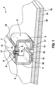
- Figure 1 shows - schematically - an unclaimed example of a contact arrangement 1.
- the contact arrangement 1 has a connecting element 2.
- the connecting element 2 is U-shaped in this example.
- the connecting element 2 has a spacer leg 3 and a spacer leg 4 spaced parallel to the spacer leg 3.
- the spacer legs 3 and 4 are each formed by an angled section of a sheet metal strip.
- the spacer legs 3 and 4 are each connected to one another via a connecting section 5.
- the spacer legs 3 and 4 each extend orthogonally to the connecting section 5.
- a fastening foot 14 is formed on the spacer leg 3 and extends transversely to the spacer leg 3, facing away from the connecting section 5.
- a fastening foot 15 is formed on the spacer leg 4 and extends transversely to the spacer leg 4 and extends parallel to the connecting section 5.
- the connecting element 2 is formed from a sheet metal strip, in particular a copper sheet strip, by angling the above-mentioned partial sections such as the fastening foot 15, the spacer leg 4, the connecting section 5, the spacer leg 3 and the fastening foot 14.
- fastening feet 14 and 15 point towards one another and extend parallel to the connecting section 5.
- the spacer legs 3 and 4 are each designed as a sheet metal strip section, and thus - as a leaf spring - designed to be resilient, with an additional spring being formed by the bend to the respective fastening foot and to the connecting section 5.
- the connecting section 5 has an opening 6 for connecting to a busbar 7.
- the busbar 7 is formed by a sheet metal strip, in particular a copper sheet strip.
- the busbar 7 has an opening 8 for connection, in this example for rivet connection, to the connection section 5.
- the contact arrangement 1 also includes a rivet element 9.
- the rivet element 9 is arranged with a longitudinal section in the opening 6 and in a longitudinal section of the rivet element 9 arranged adjacent thereto in the opening 8.
- the rivet element 9 has a rivet head 10 which is formed by a radially repelling collar and which is designed to engage positively behind an edge in the region of the opening 8 of the connecting section 5.
- the rivet element 9 also has a rivet head 11, which extends radially to repel and is designed to engage behind the busbar 7 in the area of the opening 8 in a form-fitting manner.
- the rivet element 9 is designed to press the busbar 7 and the connecting section 5 together and to keep them connected.
- the rivet head 10 and / or the rivet head 11 are each made by cold forming, for example by means of an - in Figure 1 Not shown - rivet pliers, which can engage to connect the busbar 7 with the connecting portion 5 in the cavity 35.
- the fastening foot 15 is connected to an electrically conductive layer 20 of a circuit carrier 18 by means of a solder 16.
- the fastening foot 14 is connected to the electrically conductive layer 20 by means of a solder 17.
- the fastening feet 14 and 15 are soldered to the electrically conductive layer 20, for example by means of reflow soldering in a soldering furnace.
- the electrically conductive layer 20 is connected with its flat extension to a further layer, namely an electrically insulating layer 19.
- the electrically insulating layer 19 is formed by a ceramic layer.
- the connecting element 2 encloses a cavity 35 with the aforementioned U-shape, in which the spacer legs 3 and 4 each form a U-leg.
- a pliers jaw of rivet pliers can engage in the cavity 35 to connect the busbar 7 to the connecting section 5.
- the rivet pliers can thus grip around the connecting section 5 and the busbar 7 lying together on top of one another for cold forming the rivet element 9 to form the rivet head 11, or additionally the rivet head 10.
- the busbar 7 can be connected to the connecting section 5 by means of a welded connection 12 formed by a welding bead.
- the busbar 7 can be connected to the connection section 5 additionally or independently of the rivet element 9 and the welded connection 12 by means of a resistance welded connection 13, in this example formed by a welded spot.
- a welding gun can engage with a jaw in the cavity 35 and press onto the busbar 7 with a further jaw and press the busbar 7 and the connecting section 5 together and connect them to one another by means of a welding current to produce the weld 13.
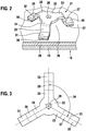
- Figure 2 shows - schematically - an embodiment for a connecting element 21, which instead of in Figure 1 Connection element 2 shown can be connected to the busbar 7 and the circuit carrier 18 as part of the contact arrangement 1.
- the connecting element 21 has a connecting section 22, which in this exemplary embodiment is formed by a sheet-metal element that is round at least in sections.
- the connecting section 22 in this exemplary embodiment is connected to a spring arm 23, a spring arm 24 and a spring arm 25, which are each molded onto the connecting section 22 and extend radially away from the connecting section 22.
- the connecting element 21 also has a spacer leg 27 which is integrally formed on the spring arm 23 and extends transversely to the spring arm 23.
- the connecting element 21 also has a spacer leg 28 which is integrally formed on the spring arm 24 and extends transversely.
- a spacer leg 29 extending transversely to the spring arm 25 is formed on the spring arm 25.
- a fastening foot 30 is formed on the spacer leg 27 and extends from the connecting section 22 in a particularly radially repellent manner.
- a fastening foot 31 is formed on the spacer leg 28, which angled relative to the spacer leg 28 and extends in particular radially away from the connecting section 22.
- a fastening foot 32 is molded onto the spacer leg 29 and extends from the connecting section 22, in particular in a radially repellent manner.
- the fastening foot 30 is soldered to the circuit carrier by means of a solder 37, the fastening foot 31 by means of a solder 38 and the fastening foot 32 by means of a solder 39.
- the mounting feet 30, 31, and 32 can be different than in Figure 2 shown, can also be arranged pointing radially inward to the connecting section 22.
- a breakthrough 26 is formed in the connecting section 22, so that the connecting section 22 can be electrically conductively and mechanically connected to a busbar by means of a rivet element or a screw element.
- Figure 3 shows a stamped or laser-cut sheet metal piece in this embodiment, from which by folding parts of the sheet in Figure 2 Connection element 21 shown can be generated.
- a sheet metal strip extends radially outward from the centrally arranged connecting section 22 with the opening 26 arranged centrally in the connecting section 22 to form the spring arm 23, the spacer leg 27 and the fastening foot 30.
- the fastening foot 30 can be formed by angling it along an articulated line 33.
- the longitudinal section of the sheet metal strip for the spacer leg 27 can be angled away from the spring arm 23.
- a broken line is marked with a dashed line.
- a further sheet metal strip is also connected in a radially repellent manner to the connecting section 22.
- a longitudinal section of the sheet metal strip is designed to form a spring arm 25, and a longitudinal section arranged radially outward to the longitudinal section for the spring arm is used to form the in Figure 2 shown spacer leg 29 formed.
- An end portion of the sheet metal strip is formed to form the mounting foot 32.
- the spacer leg 29 can thus be produced by angling the longitudinal section for the spacer leg 29 along a broken line shown in broken lines.
- the fastening foot 32 can be angled away from the spacer leg 29.
- a radially repellent sheet metal strip comprising a longitudinal section for producing the spring arm 24, further radially outward a longitudinal section for producing the spacer leg 28 and then an end section for producing the fastening foot 31.
- the fastening foot 31 and the spacer leg 28 can each be bent by angling the Sheet metal strips are generated on the broken lines shown in dashed lines.
- the sheet metal strip comprising the longitudinal section for the spacer leg 27 and the sheet metal strip comprising the longitudinal section for the spacer leg 29 are each arranged adjacent to one another in the circumferential direction around the opening 26 and form an angle 34 between them.
- the angle 34 is 120 degrees in this embodiment.
- the spring arms 23, 24 and 25 and the spacer legs 27, 28 and 29 formed thereon extend radially outward starting from the connecting section 22.
Landscapes
- Engineering & Computer Science (AREA)
- Manufacturing & Machinery (AREA)
- Connections Effected By Soldering, Adhesion, Or Permanent Deformation (AREA)
Description
- Die Erfindung betrifft eine Kontaktanordnung. Die Kontaktanordnung weist einen Schaltungsträger auf, insbesondere einen DBC-Schaltungsträger, AMB-Schaltungsträger oder einen HTTC- oder LTCC-Schaltungsträger. Der Schaltungsträger weist wenigstens eine elektrisch isolierende Schicht und wenigstens eine mit der elektrisch isolierenden Schicht - insbesondere aufeinanderliegend - verbundene elektrisch leitfähige Schicht auf. Die Kontaktanordnung weist auch eine Stromschiene auf, welche mit der elektrisch leitfähigen Schicht des Schaltungsträgers elektrisch verbunden ist.
EP 2 028 692 A1 offenbart eine Kontaktanordnung gemäß dem Oberbegriff von Anspruch 1. - Erfindungsgemäß weist der Schaltungsträger ein elektrisch leitfähiges, federnd ausgebildetes Verbindungselement auf. Das Verbindungselement weist wenigstens einen Befestigungsfuß, bevorzugt wenigstens zwei Befestigungsfüße auf, wobei der Befestigungsfuß mit der elektrisch leitfähigen Schicht stoffschlüssig verbunden, insbesondere mittels eines Lotmittels lötverbunden, mittels eines Sintermaterials sinterverbunden, oder mittels eines elektrisch leitfähigen Klebstoffs klebeverbunden ist. Das Verbindungselement weist auch einen von dem Schaltungsträger beabstandet angeordneten Verbindungsabschnitt zum Verbinden mit der Stromschiene auf. Der Verbindungsabschnitt ist über ein Abstandsbein mit dem Befestigungsfuß verbunden. Die Stromschiene ist bevorzugt mit dem Verbindungsabschnitt elektrisch und mechanisch verbunden. So kann der Schaltungsträger vorteilhaft über das Verbindungselement mit der Stromschiene elektrisch verbunden sein, wobei über die Stromschiene einwirkende Vibrationen oder Bewegungen der Stromschiene, insbesondere Relativbewegungen zwischen der Stromschiene und dem Schaltungsträger, welche beispielsweise durch Temperaturwechsel verursacht werden, über das federnd ausgebildete Verbindungselement vorteilhaft abgefangen werden können. Weiter vorteilhaft kann so die Stromschiene mittels eines aufwandsgünstigen und haltbaren elektrischen und mechanischen Verbindungsverfahren mit dem Abstandselement, und so mit dem Schaltungsträger, elektrisch verbunden werden. Beispielsweise kann zum Verbinden der Stromschiene mit dem Schaltungsträger das Verbindungselement gemeinsam mit anderen elektronischen Bauelementen in einem Reflow-Lötofen mit dem Schaltungsträger verlötet werden. Anschließend kann in einem weiteren Verbindungsschritt die Stromschiene mit dem Verbindungselement verlötet, verschweißt, vernietet oder verschraubt werden. So kann vorteilhaft auch eine beim Verbinden der Stromschiene mit dem Verbindungselement entstehende Kraft, Temperatur oder Vibration nicht unmittelbar auf den Schaltungsträger wirken und dort beispielsweise zu einer Delamination von elektrisch leitfähigen und elektrisch isolierenden Schichten oder einer Schädigung weiterer elektronischer Bauelemente führen.
- Der Schaltungsträger ist bevorzugt ein keramischer Schaltungsträger, insbesondere ein DBC-Schaltungsträger (DBC = Direct-Bonded-Copper), AMB-Schaltungsträger (AMB = Active-Metal-Brazed) oder ein HTTC-Schaltungsträger (HTCC = High-Temperature-Cofired-Ceramics) oder LTCC-Schaltungsträger (LTCC = Low-Temperature-Cofired-Ceramics). Der keramsiche Schaltungsträger kann durch das Verbindungselement vorteilhaft bei einer Krafteinwirkung über die Stromschiene nicht zerbrechen.
- Die Stromschiene ist bevorzugt durch einen Blechabschnitt, einen Blechstreifen, ein gestanztes oder lasergeschnittenes Blechstück, auch Lead-Frame oder Stanzgitter genannt, gebildet. Bevorzugt ist im Querschnitt der Stromschiene eine Breitenerstreckung größer als eine Dickenerstreckung. Eine Dickenerstreckung beträgt beispielsweise zwischen 0,5 und 5 Millimeter.
- Bevorzugt ist der Verbindungsabschnitt durch einen Blechabschnitt gebildet, welcher einen Oberflächenbereich zum Kontaktiertwerden durch die Stromschiene aufweist. Der Verbindungsabschnitt ist bevorzugt federnd ausgebildet, und kann - beispielsweise nach Art einer Blattfeder - quer zu seiner flachen Erstreckung einfedern.
- In einer bevorzugten Ausführungsform ist der Verbindungsabschnitt über einen radial abweisenden Federarm mit dem Abstandsbein verbunden. Der Federarm ist bevorzugt durch eine Blattfeder gebildet. So kann der Verbindungsabschnitt vorteilhaft quer zu einer flachen Erstreckung des Schaltungsträgers einfedern.
- Erfindungsgemäß weist das Verbindungselement drei jeweils federnd ausgebildete Abstandsbeine auf, welche jeweils einen Befestigungsfuß aufweisen und welche jeweils an einen Federarm angeformt sind. So kann vorteilhaft eine stabile Anordnung zum Befestigen der Stromschiene mit dem Schaltungsträger gebildet sein, wobei weiter vorteilhaft Kräfte oder Bewegungen, welche von der Stromschiene parallel zu einer flachen Erstreckung des Schaltungsträgers auf dem Verbindungsabschnitt einwirken, durch die Abstandsbeine federnd abgefangen werden können.
- Bevorzugt erstrecken sich die Abstandsbeine jeweils in einem vorbestimmten Winkel zur flachen Erstreckung des Schaltungsträgers. Der vorbestimmte Winkel ist beispielsweise ein rechter Winkel, sodass die Abstandsbeine sich mit ihrer Längserstreckung quer zu einer flachen Erstreckung des Verbindungsabschnitts, und so auch quer zum Schaltungsträger, erstrecken. Dadurch kann vorteilhaft eine Federeigenschaft des Abstandsbeins gebildet sein.
- Vorteilhaft ist durch die Abstandsbeine zwischen dem Verbindungsabschnitt und dem Schaltungsträger ein Hohlraum gebildet, sodass zum Verbinden des Verbindungsabschnitts mit der Stromschiene ein Werkzeug, beispielsweise eine Zange zum Widerstandsschweißen oder eine Zange zum Vernieten der Stromschiene mit dem Verbindungsabschnitt, in den Hohlraum eingreifen kann.
- Die Federarme erstrecken sich jeweils erfindungsgemäß in der flachen Erstreckung des Verbindungsabschnitts radial abweisend. Weiter erfindungsgemäß schließen zueinander unmittelbar benachbarte Federarme einen Winkel von 120 Grad zwischeneinander ein. So ist vorteilhaft eine sternförmige Anordnung der Federarme und der Abstandsbeine gebildet, sodass Bewegungen der Stromschiene, welche parallel zum Schaltungsträger auf das Verbindungselement einwirken, aus nahezu allen Richtungen unter dem Verbindungsabschnitt umlaufend von dem Verbindungselement, insbesondere dem Abstandsbeinen, federnd abgefangen werden können.
- In einer bevorzugten Ausführungsform der Kontaktanordnung ist das Verbindungselement mit der Stromschiene mittels wenigstens eines Nietelements vernietet. Das Nietelement ist bevorzugt ein Metall-Nietelement, weiter bevorzugt ein Kupfer-Nietelement. Bevorzugt weist die Stromschiene und der Verbindungsabschnitt jeweils einen Durchbruch zum Durchführen des Nietelements auf. So kann das Verbindungselement vorteilhaft einfach und aufwandsgünstig mittels einer Nietzange und eines Nietelements mit der Stromschiene elektrisch leitfähig, insbesondere galvanisch durch Berühren elektrisch leitend, und mechanisch fest verbunden werden.
- In einer bevorzugten Ausführungsform ist das Verbindungselement mit der Stromschiene verschweißt, insbesondere mittels Widerstandsschweißen verschweißt. So kann die Stromschiene vorteilhaft zum elektrischen und mechanischen Verbinden auf das Verbindungselement, insbesondere den Verbindungsabschnitt, aufgelegt werden, wobei in einem weiteren Verbindungsschritt eine Widerstandsschweißzange in den zwischen dem Verbindungsabschnitt und dem Schaltungsträger verbleibenden Hohlraum eingreifen kann und so die Stromschiene und den Verbindungsabschnitt zwischen zwei Zangenbacken festhalten und miteinander verschweißen kann.
- In einer bevorzugten Ausführungsform ist das Verbindungselement mit der Stromschiene verlötet, insbesondere mittels Hartlöten verlötet, oder mittels Weichlöten, insbesondere Selektivweichlöten verlötet. So kann die Stromschiene vorteilhaft in einem weiteren Verbindungsschritt nach einem Reflow-Verlöten des Schaltungsträgers mit dem Verbindungselement oder zusätzlich mit weiteren elektronischen Bauelementen mit dem Verbindungselement selektivverlötet werden.
- In einer bevorzugten Ausführungsform erstrecken die Abstandsbeine sich quer zu einer flachen Erstreckung des Verbindungsabschnitts. So kann vorteilhaft platzsparend ein Hohlraum zwischen dem Verbindungsabschnitt und dem Schaltungsträger gebildet sein. Die Abstandsbeine erstrecken sich bevorzugt jeweils parallel zueinander beabstandet.
- In einer bevorzugten Ausführungsform sind die Stromschiene und das Verbindungselement jeweils aus Blech, insbesondere aus Kupferblech, gebildet. Bevorzugt ist die Legierung eine Legierung Legierung umfassend Kupfer und Zinn, insbesondre eine CuSn6-Kupferlegierung oder eine CuSn0.15-Kupferlegierung, beispielsweise gemäß der Norm UNS C14415. Bevorzugt ist das Kupferblech aus einer Kupferlegierung gemäß der Norm UNS C18080 gebildet. Die Kupferlegierung weist bevorzugt eine Beimengung umfassend Chrom, Silber, Eisen, Titan, Silizium und zum größten Teil Kupfer auf. Die Anteile der Beimengung betragen jeweils bevorzugt 0,5 % Chrom, 0,1 % Silber, 0,08 % Eisen, 0,06 % Titan und 0,03 % Silizium. Eine elektrische Leitfähigkeit des Verbindungselements beträgt bevorzugt wenigstens 30, bevorzugt 46 Mega-Siemens pro Meter.
- So kann sowohl die Stromschiene, als auch das Verbindungselement vorteilhaft durch Stanzen oder durch Laserschneiden aus einem Blech erzeugt werden. Das Verbindungselement, insbesondere die zuvor erwähnten Teile des Verbindungselements, umfassend den Verbindungsabschnitt, die Federarme, die Abstandsbeine und die Befestigungsfüße, können vorteilhaft nach einem Ausstanzen eines Roh-Verbindungselements aus einem flachen Blech durch Abwinkeln an Knicklinien erzeugt werden. Der Verbindungsabschnitt kann beispielsweise durch eine zentral angeordnete Platte aus Blech gebildet sein, wobei an die Platte radial abweisende Blechstreifen zum Ausbilden der Abstandsbeine und der Befestigungsfüße oder zusätzlich der Federarme angeformt sind.
- Das Abstandsbein kann so beispielsweise durch Abwinkeln des Blechstreifens erzeugt werden, wobei ein sich zwischen der Platte als Verbindungsabschnitt und dem Abstandsbein erstreckender Blechstreifen den Federarm ausbilden kann. Das Abstandsbein kann mit einem Endabschnitt abgewinkelt werden, sodass so auf einfache Weise der Befestigungsfuß gebildet ist, welcher an das Abstandsbein angeformt ist.
- Ein nicht beanspruchtes Beispiel betrifft auch ein Verfahren zum Verbinden eines Schaltungsträgers mit einer Stromschiene. Der Schaltungsträger weist eine elektrisch leitfähige Schicht und eine elektrisch isolierende Schicht auf. Bei dem Verfahren wird ein elektrisch leitfähiges und federnd ausgebildetes Verbindungselement, umfassend einen Verbindungsabschnitt zum Verbinden mit der Stromschiene und wenigstens zwei mit dem Verbindungsabschnitt verbundene Befestigungsfüße, mit den Befestigungsfüßen mit der elektrisch leitfähigen Schicht verlötet, sodass ein Verbindungsabschnitt von dem Schaltungsträger beabstandet ist. Bei dem Verfahren wird der Verbindungsabschnitt und ein Endabschnitt der Stromschiene elektrisch leitfähig und mechanisch fest miteinander vernietet oder verschweißt.
- Bevorzugt greift zum Verschweißen eine zum Schweißverbinden ausgebildete Zange in eine zwischen dem Verbindungsabschnitt und dem Schaltungsträger gebildeten Hohlraum ein. Weiter bevorzugt wird der Endabschnitt der Stromschiene und der Verbindungsabschnitt von der zum Schweißverbinden ausgebildeten Zange umgriffen und mittels Widerstandsschweißen miteinander verschweißt.
- Bevorzugt greift eine zum Vernieten ausgebildete Zange in einen zwischen dem Verbindungsabschnitt und dem Schaltungsträger gebildeten Hohlraum ein. Weiter bevorzugt umgreift die zum Vernieten ausgebildete Zange den Endabschnitt der Stromschiene und den Verbindungsabschnitt und führt ein Nietelement durch einen in dem Endabschnitt und in dem Verbindungsabschnitt jeweils ausgebildeten Durchbruch und verpresst das Nietelement derart, dass das Nietelement den Verbindungsabschnitt und den Endabschnitt der Stromschiene jeweils formschlüssig hintergreift.
- Bevorzugt ist die Kontaktanordnung ausgebildet, einen Strom zwischen 100 und 600 Ampere über die Stromschiene und das Verbindungselement zu führen.
- Die Erfindung wird nun im Folgenden anhand von Figuren und weiteren Ausführungsbeispielen beschrieben. Weitere vorteilhafte Ausführungsvarianten ergeben sich aus den in den Figuren und in den abhängigen Ansprüchen beschriebenen Merkmalen.
-
Figur 1 zeigt ein nicht beanspruchtes Beispiel für eine Kontaktanordnung umfassend einen Schaltungsträger, der über ein Verbindungselement mit einer Stromschiene verbunden ist; -
Figur 2 zeigt ein Ausführungsbeispiel für ein Verbindungselement, das drei federnd ausgebildete Abstandsbeine aufweist; -
Figur 3 zeigt eine Aufsicht auf ein Blechstück, das zum Ausbilden des inFigur 2 gezeigten Verbindungselements an Knicklinien abgewinkelt werden kann. -
Figur 1 zeigt - schematisch - ein nicht beanspruchtes Beispiel für eine Kontaktanordnung 1. Die Kontaktanordnung 1 weist ein Verbindungselement 2 auf. Das Verbindungselement 2 ist in diesem Beispiel U-förmig ausgebildet. Das Verbindungselement 2 weist ein Abstandsbein 3 auf und ein zu dem Abstandsbein 3 parallel beabstandetes Abstandsbein 4. Die Abstandsbeine 3 und 4 sind jeweils durch einen abgewinkelten Abschnitt eines Blechstreifens gebildet. Die Abstandsbeine 3 und 4 sind jeweils über einen Verbindungsabschnitt 5 miteinander verbunden. Die Abstandsbeine 3 und 4 erstrecken sich jeweils orthogonal zu dem Verbindungsabschnitt 5. - An das Abstandsbein 3 ist ein Befestigungsfuß 14 angeformt, welcher sich quer zu dem Abstandsbein 3, von dem Verbindungsabschnitt 5 abweisend erstreckt. An das Abstandsbein 4 ist ein Befestigungsfuß 15 angeformt, welcher sich quer zu dem Abstandsbein 4 und sich parallel zu dem Verbindungsabschnitt 5 erstreckt.
- Das Verbindungselement 2 ist in diesem Beispiel aus einem Blechstreifen, insbesondere Kupferblechstreifen, durch Abwinkeln der zuvor genannten Teilabschnitte wie den Befestigungsfuß 15, das Abstandsbein 4, den Verbindungsabschnitt 5, das Abstandsbein 3 und den Befestigungsfuß 14 gebildet. Die Befestigungsfüße 14 und 15 weisen in diesem Ausführungsbeispiel aufeinander zu und erstrecken sich parallel zu dem Verbindungsabschnitt 5.
- In einer anderen - in
Figur 1 nicht dargestellten - beispielhaften Form weisen die Befestigungsfüße 14 und 15 jeweils voneinander ab. - Die Abstandsbeine 3 und 4 sind jeweils als Blechstreifenabschnitt ausgebildet, und so - als Blattfeder- federnd ausgebildet, wobei eine zusätzliche Feder durch die Abwinkelung zu dem jeweiligen Befestigungsfuß und zu dem Verbindungsabschnitt 5 hin gebildet ist.
- Der Verbindungsabschnitt 5 weist in diesem Beispiel einen Durchbruch 6 zum Verbinden mit einer Stromschiene 7 auf. Die Stromschiene 7 ist in diesem Beispiel durch einen Blechstreifen, insbesondere Kupferblechstreifen, gebildet. Die Stromschiene 7 weist einen Durchbruch 8 zum Verbinden, in diesem Beispiel zum Nietverbinden, mit dem Verbindungsabschnitt 5 auf. Die Kontaktanordnung 1 umfasst in diesem Ausführungsbeispiel auch ein Nietelement 9. Das Nietelement 9 ist in diesem Beispiel mit einem Längsabschnitt in dem Durchbruch 6 angeordnet und in einem dazu benachbart angeordneten Längsabschnitt des Nietelements 9 in dem Durchbruch 8 angeordnet. Das Nietelement 9 weist einen Nietkopf 10 auf, welcher durch einen radial abweisenden Kragen gebildet ist und welcher ausgebildet ist, einen Rand im Bereich des Durchbruchs 8 des Verbindungsabschnitts 5 formschlüssig zu hintergreifen. Das Nietelement 9 weist in diesem Beispiel auch einen Nietkopf 11 auf, welcher sich radial abweisend erstreckt und ausgebildet ist, die Stromschiene 7 im Bereich des Durchbruchs 8 formschlüssig zu hintergreifen. Das Nietelement 9 ist ausgebildet, die Stromschiene 7 und den Verbindungsabschnitt 5 einander zusammenzupressen und verbunden zu halten.
- Der Nietkopf 10 und/oder der Nietkopf 11 sind jeweils durch Kaltumformen, beispielsweise mittels einer - in
Figur 1 nicht dargestellten - Nietzange, erzeugt, welche zum Verbinden der Stromschiene 7 mit dem Verbindungsabschnitt 5 in den Hohlraum 35 eingreifen kann. - Der Befestigungsfuß 15 ist in diesem Beispiel mittels eines Lotmittels 16 mit einer elektrisch leitfähigen Schicht 20 eines Schaltungsträgers 18 verbunden. Der Befestigungsfuß 14 ist mittels eines Lotmittels 17 mit der elektrisch leitfähigen Schicht 20 verbunden. Die Befestigungsfüße 14 und 15 sind beispielsweise mittels Reflow-Löten in einem Lötofen mit der elektrisch leitfähigen Schicht 20 verlötet. Die elektrisch leitfähige Schicht 20 ist in diesem Ausführungsbeispiel mit ihrer flachen Erstreckung mit einer weiteren Schicht, nämlich einer elektrisch isolierenden Schicht 19, verbunden. Die elektrisch isolierende Schicht 19 ist in diesem Beispiel durch eine Keramikschicht gebildet. Der Schaltungsträger 8 ist in diesem Beispiel durch ein DBC-Substrat (DBC = Direct-Bonded-Copper) gebildet.
- Das Verbindungselement 2 umschließt mit der zuvor genannten U-Form, bei der die Abstandsbeine 3 und 4 jeweils einen U-Schenkel bilden, einen Hohlraum 35. In den Hohlraum 35 kann zum Verbinden der Stromschiene 7 mit dem Verbindungsabschnitt 5 eine Zangenbacke einer Nietzange eingreifen. Die Nietzange kann so zum Kaltumformen des Nietelements 9 zum Ausbilden des Nietkopfes 11, oder zusätzlich des Nietkopfes 10, den Verbindungsabschnitt 5 und die Stromschiene 7 gemeinsam aufeinanderliegend umgreifen.
- Anstelle des Nietelements 9 oder zusätzlich zu dem Nietelement 9 kann die Stromschiene 7 mit dem Verbindungsabschnitt 5 mittels einer Schweißverbindung 12, gebildet durch eine Schweißraupe, verbunden sein.
- Die Stromschiene 7 kann mit dem Verbindungsabschnitt 5 zusätzlich oder unabhängig von dem Nietelement 9 und der Schweißverbindung 12 mittels einer Widerstands-Schweißverbindung 13, in diesem Beispiel gebildet durch einen Schweißpunkt, stoffschlüssig verbunden sein. Zum Erzeugen der Widerstandsschweißverbindung 13 kann eine Schweißzange mit einer Zangenbacke in den Hohlraum 35 eingreifen und mit einer weiteren Zangenbacke auf die Stromschiene 7 pressen und die Stromschiene 7 und den Verbindungsabschnitt 5 einander zusammenpressen und mittels eines Schweißstromes unter Erzeugung der Schweißverbindung 13 stoffschlüssig miteinander verbinden.
-
Figur 2 zeigt - schematisch - ein Ausführungsbeispiel für ein Verbindungselement 21, welches anstelle des inFigur 1 gezeigten Verbindungselements 2 mit der Stromschiene 7 und dem Schaltungsträger 18 als Bestandteil der Kontaktanordnung 1 verbunden sein kann. Das Verbindungselement 21 weist einen Verbindungsabschnitt 22 auf, welcher in diesem Ausführungsbeispiel durch ein wenigstens umfangsabschnittsweise rund ausgebildetes Blechelement gebildet ist. Der Verbindungsabschnitt 22 in diesem Ausführungsbeispiel mit einem Federarm 23, einem Federarm 24 und einem Federarm 25 verbunden, welche jeweils an den Verbindungsabschnitt 22 angeformt sind und sich radial abweisend von dem Verbindungsabschnitt 22 erstrecken. - Das Verbindungselement 21 weist auch ein Abstandsbein 27 auf, welches an den Federarm 23 angeformt ist und sich quer zu dem Federarm 23 erstreckt. Das Verbindungselement 21 weist auch ein Abstandsbein 28 auf, welches sich quer erstreckend an den Federarm 24 angeformt ist. An den Federarm 25 ist ein sich zu dem Federarm 25 quer erstreckendes Abstandsbein 29 angeformt.
- An das Abstandsbein 27 ist ein Befestigungsfuß 30 angeformt, welcher sich von dem Verbindungsabschnitt 22 insbesondere radial abweisend erstreckt. An das Abstandsbein 28 ist ein Befestigungsfuß 31 angeformt, welcher sich zu dem Abstandsbein 28 abgewinkelt und vom Verbindungsabschnitt 22 insbesondere radial abweisend erstreckt. An das Abstandsbein 29 ist ein Befestigungsfuß 32 angeformt, welcher sich von dem Verbindungsabschnitt 22 insbesondere radial abweisend erstreckt. Der Befestigungsfuß 30 ist mittels eines Lotmittels 37, der Befestigungsfuß 31 mittels eines Lotmittels 38 und der Befestigungsfuß 32 mittels eines Lotmittels 39 mit dem Schaltungsträger lötverbunden.
- Die Befestigungsfüße 30, 31, und 32 können anders als in
Figur 2 dargestellt, auch radial nach innen zu dem Verbindungsabschnitt 22 weisend angeordnet sein. - In dem Verbindungsabschnitt 22 ist ein Durchbruch 26 gebildet, sodass der Verbindungsabschnitt 22 mittels eines Nietelements oder eines Schraubelements mit einer Stromschiene elektrisch leitfähig und mechanisch verbunden werden kann.
- Dazu kann eine - in
Figur 2 nicht dargestellte - Niet- oder Schweißzange in einen zwischen dem Verbindungsabschnitt 22 und dem inFigur 1 dargestellten Schaltungsträger 18 ausgebildeten Hohlraum 36 eingreifen. -
Figur 3 zeigt ein in diesem Ausführungsbeispiel gestanztes oder lasergeschnittenes Blechstück, aus dem durch Falten von Teilen des Blechs das inFigur 2 dargestellte Verbindungselement 21 erzeugt werden kann. Von dem zentral angeordneten Verbindungsabschnitt 22 mit dem zentral in dem Verbindungsabschnitt 22 angeordneten Durchbruch 26 erstreckt sich radial nach außen ein Blechstreifen zum Ausbilden des Federarms 23, des Abstandsbeins 27 und des Befestigungsfußes 30. Der Befestigungsfuß 30 kann durch Abwinkeln entlang einer Knicklinie 33 gebildet werden. Zum Ausbilden des Abstandsbeins 27 kann der Längsabschnitt des Blechstreifens für das Abstandsbein 27 von dem Federarm 23 abgewinkelt werden. Eine Knicklinie ist gestrichelt gekennzeichnet. - Mit dem Verbindungsabschnitt 22 ist auch ein weiterer Blechstreifen radial abweisend verbunden. Ein Längsabschnitt des Blechstreifens ist zum Ausbilden eines Federarms 25 ausgebildet und ein radial nach außen zu dem Längsabschnitt für den Federarm angeordneter Längsabschnitt ist zum Ausbilden des in
Figur 2 dargestellten Abstandsbeins 29 ausgebildet. Ein Endabschnitt des Blechstreifens ist zum Ausbilden des Befestigungsfußes 32 ausgebildet. - Das Abstandsbein 29 kann so durch Abwinkeln des Längsabschnitts für das Abstandsbein 29 entlang einer gestrichelt dargestellten Knicklinie erzeugt werden. Der Befestigungsfuß 32 kann von dem Abstandsbein 29 abgewinkelt werden.
- Dargestellt ist auch ein radial abweisender Blechstreifen umfassend einen Längsabschnitt zum Erzeugen des Federarms 24, weiter radial nach außen eines Längsabschnitts zum Erzeugen des Abstandsbeins 28 und daran anschließend ein Endabschnitt zum Erzeugen des Befestigungsfußes 31. Der Befestigungsfuß 31 und das Abstandsbein 28 können jeweils durch Abwinkeln des Blechstreifens an den gestrichelt dargestellten Knicklinien erzeugt werden.
- Der Blechstreifen umfassend den Längsabschnitt für das Abstandsbein 27 und der Blechstreifen umfassend den Längsabschnitt für das Abstandsbein 29 sind jeweils in Umlaufrichtung um den Durchbruch 26 zueinander benachbart angeordnet und schließen einen Winkel 34 zwischeneinander ein. Der Winkel 34 beträgt in diesem Ausführungsbeispiel 120 Grad. Die Federarme 23, 24 und 25 und die daran angeformten Abstandsbeine 27, 28 beziehungsweise 29 erstrecken sich so ausgehend von dem Verbindungsabschnitt 22 sternförmig radial nach außen.
Claims (6)
- Kontaktanordnung (1) mit einem Schaltungsträger (18), und einer Stromschiene (7), wobei der Schaltungsträger (18) wenigstens eine elektrisch isolierende Schicht (19) und wenigstens eine mit der elektrisch isolierenden Schicht (19) verbundene elektrisch leitfähige Schicht (20) aufweist, wobei der Schaltungsträger (18) ein elektrisch leitfähiges, federnd ausgebildetes Verbindungselement (21) aufweist, wobei das Verbindungselement (21) wenigstens einen Befestigungsfuß (30, 31, 32) aufweist, welcher mit der elektrisch leitfähigen Schicht (20) lötverbunden ist, wobei das Verbindungselement (21) einen von dem Schaltungsträger (18) beabstandet angeordneten Verbindungsabschnitt (22) aufweist, wobei die Stromschiene (7) mit dem Verbindungsabschnitt (22) elektrisch und mechanisch verbunden ist, wobei das Verbindungselement (21) drei Abstandsbeine (27, 28, 29) aufweist und der Verbindungsabschnitt (22) jeweils über einen Federarm (23, 24, 25) mit dem jeweiligen Abstandsbein (27, 28, 29) verbunden ist, wobei die Abstandsbeine (27, 28, 29) jeweils einen Befestigungsfuß (30, 31, 32) aufweisen, welcher an den jeweiligen Federarm (23, 24, 25) angeformt ist,
dadurch gekennzeichnet, dass
sich die Federarme jeweils in der flachen Erstreckung des Verbindungsabschnitts radial abweisend erstrecken und zueinander unmittelbar benachbarte Federarme einen Winkel von 120 Grad zwischeneinander einschließen, sodass eine sternförmige Anordnung der Federarme und der Abstandsbeine gebildet ist. - Kontaktanordnung (1) nach Anspruch 1,
dadurch gekennzeichnet, dass
das Verbindungselement (21) mit der Stromschiene (7) mittels wenigstens eines Nietelements (9) vernietet ist. - Kontaktanordnung (1) nach Anspruch 1,
dadurch gekennzeichnet, dass
das Verbindungselement (21) mit der Stromschiene (7) verschweißt, insbesondere mittels Widerstandsschweißen verschweißt ist. - Kontaktanordnung (1) nach Anspruch 1,
dadurch gekennzeichnet, dass
das Verbindungselement (21) mit der Stromschiene (7) verlötet, insbesondere selektiv verlötet ist. - Kontaktanordnung (1) nach einem der vorhergehenden Ansprüche,
dadurch gekennzeichnet, dass
die Abstandsbeine (27, 28, 29) sich quer zu einer flachen Erstreckung des Verbindungsabschnitts (22) erstecken. - Kontaktanordnung (1) nach einem der vorhergehenden Ansprüche,
dadurch gekennzeichnet, dass
die Stromschiene (7) und das Verbindungselement (21) jeweils aus Blech, insbesondere Kupferblech gebildet sind.
Applications Claiming Priority (1)
| Application Number | Priority Date | Filing Date | Title |
|---|---|---|---|
| DE102014219585.3A DE102014219585A1 (de) | 2014-09-26 | 2014-09-26 | Kontaktanordnung mit einem Schaltungsträger und einem Verbindungselement |
Publications (2)
| Publication Number | Publication Date |
|---|---|
| EP3001508A1 EP3001508A1 (de) | 2016-03-30 |
| EP3001508B1 true EP3001508B1 (de) | 2020-06-17 |
Family
ID=54150268
Family Applications (1)
| Application Number | Title | Priority Date | Filing Date |
|---|---|---|---|
| EP15185446.0A Active EP3001508B1 (de) | 2014-09-26 | 2015-09-16 | Kontaktanordnung mit einem schaltungsträger und einem verbindungselement |
Country Status (2)
| Country | Link |
|---|---|
| EP (1) | EP3001508B1 (de) |
| DE (1) | DE102014219585A1 (de) |
Families Citing this family (8)
| Publication number | Priority date | Publication date | Assignee | Title |
|---|---|---|---|---|
| DE102019111963A1 (de) * | 2019-05-08 | 2020-11-12 | Danfoss Silicon Power Gmbh | Halbleitermodul mit einem Halbleiter und mit einem Metallformteil, der vom Halbleiter elektrisch kontaktiert wird |
| DE102019111964A1 (de) | 2019-05-08 | 2020-11-12 | Danfoss Silicon Power Gmbh | Halbleitermodul mit einem ersten Substrat, einem zweiten Substrat und einen Abstandhalter, der die Substrate voneinander trennt |
| EP3748675A1 (de) * | 2019-06-04 | 2020-12-09 | Siemens Aktiengesellschaft | Leistungshalbleitermodul mit gestaffelten anschlussflächen |
| DE102020207398A1 (de) | 2020-06-16 | 2021-12-16 | Mahle International Gmbh | Kontaktierungsstück |
| US11374366B2 (en) | 2020-06-19 | 2022-06-28 | Lear Corporation | System and method for providing an electrical ground connection for a circuit assembly |
| DE102020120778B4 (de) | 2020-08-06 | 2023-03-23 | Lisa Dräxlmaier GmbH | Stromschiene für ein kraftfahrzeug und verfahren zum herstellen einer stromschiene |
| US11646514B2 (en) | 2020-08-10 | 2023-05-09 | Lear Corporation | Surface mount technology terminal header and method for providing an electrical connection to a printed circuit board |
| US11706867B2 (en) | 2021-01-27 | 2023-07-18 | Lear Corporation | System and method for providing an electrical ground connection for a circuit assembly |
Family Cites Families (8)
| Publication number | Priority date | Publication date | Assignee | Title |
|---|---|---|---|---|
| DE20313285U1 (de) * | 2003-08-27 | 2004-09-30 | Weco Wester, Ebbinghaus Gmbh & Co. Kg | Elektrische Anschlussklemme |
| DE102006014582B4 (de) * | 2006-03-29 | 2011-09-15 | Infineon Technologies Ag | Halbleitermodul |
| US8129836B2 (en) * | 2006-06-09 | 2012-03-06 | Honda Motor Co., Ltd. | Semiconductor device |
| JP5103863B2 (ja) * | 2006-10-16 | 2012-12-19 | 富士電機株式会社 | 半導体装置 |
| DE112008003425B4 (de) * | 2007-12-20 | 2023-08-31 | Aisin Aw Co., Ltd. | Verfahren zum Herstellen eines Halbleiterbauelements |
| JP5126617B2 (ja) * | 2009-05-27 | 2013-01-23 | アイシン・エィ・ダブリュ株式会社 | 半導体装置及び接続部材 |
| JP5585547B2 (ja) * | 2011-07-06 | 2014-09-10 | 株式会社デンソー | 端子台 |
| FR2990795B1 (fr) * | 2012-05-16 | 2015-12-11 | Sagem Defense Securite | Agencement de module electronique de puissance |
-
2014
- 2014-09-26 DE DE102014219585.3A patent/DE102014219585A1/de not_active Withdrawn
-
2015
- 2015-09-16 EP EP15185446.0A patent/EP3001508B1/de active Active
Non-Patent Citations (1)
| Title |
|---|
| None * |
Also Published As
| Publication number | Publication date |
|---|---|
| EP3001508A1 (de) | 2016-03-30 |
| DE102014219585A1 (de) | 2016-03-31 |
Similar Documents
| Publication | Publication Date | Title |
|---|---|---|
| EP3001508A1 (de) | Kontaktanordnung mit einem schaltungsträger und einem verbindungselement | |
| EP1403968B1 (de) | Anschlussklemme | |
| DE102013013458B3 (de) | Kontaktelement | |
| DE10149574C2 (de) | Stanzgitter mit einem Messeraufnahmekontakt | |
| DE102008022794A1 (de) | Elektrisches Schutzbauelement mit Kurzschlusseinrichtung | |
| DE102009046489A1 (de) | Schutzeinrichtung für eine elektrische Schaltung | |
| WO2018007129A1 (de) | Elektrischer hochleistungskontakt | |
| EP2867954B1 (de) | Kontaktelement zum verbinden mit einer leiterplatte, kontaktsystem und verfahren | |
| EP2297820B1 (de) | Schutzleiteranschlussvorrichtung aus metall | |
| WO2018011195A1 (de) | Elektronische baugruppe mit thermosicherung | |
| EP1313109A2 (de) | Oberflächenmontierbarer elektrischer Widerstand | |
| DE102011005655A1 (de) | Kontaktelement und Verfahren zu dessen Herstellung | |
| EP1459331A2 (de) | Federbügel, überspannungsableiter mit dem federbügel und anordnung eines überspannungsableiters | |
| DE102013201556B4 (de) | Batteriesystem mit einem Kontaktelement | |
| EP2551963B1 (de) | Elektrisches Anschlusselement | |
| DE102009044933B4 (de) | Leistungshalbleitermodul mit mindestens zwei verbundenen Schaltungsträgern und Verfahren zur Herstellung eines Leistungshalbleitermoduls mit mindestens zwei verbundenen Schaltungsträgern | |
| EP1898496A1 (de) | Metallisches Kontaktelement für eine elektrische Kontaktanordnung | |
| EP3571446B1 (de) | Sicherheitsvorrichtung zum notabschalten eines elektrischen durchlauferhitzers | |
| DE102014219229A1 (de) | Kontaktsystem mit einem Schaltungsträger und einer nietverbundenen Stromschiene | |
| WO2021023539A9 (de) | WERKZEUG ZUM FIXIEREN EINES BAUTEILS ZUM STOFFSCHLÜSSIGEN FÜGEN, VERFAHREN ZUM ULTRASCHALLSCHWEIßEN | |
| DE102015104667B4 (de) | Oberflächenmontierbares stromkontaktelement zur montage an einer leiterplatte, damit ausgestattete leiterplatte und montageverfahren | |
| EP2425498B1 (de) | Verbindungssystem für platine mit einer gedruckten schaltung | |
| DE102019108563B4 (de) | Leiterplattenanschlussklemme | |
| EP3002997B1 (de) | Elektrisches bauteil mit einem eingriffselement | |
| DE202016100931U1 (de) | Sicherungssockel |
Legal Events
| Date | Code | Title | Description |
|---|---|---|---|
| PUAI | Public reference made under article 153(3) epc to a published international application that has entered the european phase |
Free format text: ORIGINAL CODE: 0009012 |
|
| AK | Designated contracting states |
Kind code of ref document: A1 Designated state(s): AL AT BE BG CH CY CZ DE DK EE ES FI FR GB GR HR HU IE IS IT LI LT LU LV MC MK MT NL NO PL PT RO RS SE SI SK SM TR |
|
| AX | Request for extension of the european patent |
Extension state: BA ME |
|
| 17P | Request for examination filed |
Effective date: 20160930 |
|
| RBV | Designated contracting states (corrected) |
Designated state(s): AL AT BE BG CH CY CZ DE DK EE ES FI FR GB GR HR HU IE IS IT LI LT LU LV MC MK MT NL NO PL PT RO RS SE SI SK SM TR |
|
| STAA | Information on the status of an ep patent application or granted ep patent |
Free format text: STATUS: EXAMINATION IS IN PROGRESS |
|
| 17Q | First examination report despatched |
Effective date: 20180221 |
|
| GRAP | Despatch of communication of intention to grant a patent |
Free format text: ORIGINAL CODE: EPIDOSNIGR1 |
|
| STAA | Information on the status of an ep patent application or granted ep patent |
Free format text: STATUS: GRANT OF PATENT IS INTENDED |
|
| INTG | Intention to grant announced |
Effective date: 20200109 |
|
| RIC1 | Information provided on ipc code assigned before grant |
Ipc: H01R 12/57 20110101AFI20191213BHEP Ipc: H01R 12/70 20110101ALN20191213BHEP Ipc: H01R 43/02 20060101ALI20191213BHEP Ipc: H01L 23/498 20060101ALI20191213BHEP Ipc: H01R 12/91 20110101ALI20191213BHEP |
|
| RAP1 | Party data changed (applicant data changed or rights of an application transferred) |
Owner name: ROBERT BOSCH GMBH |
|
| GRAS | Grant fee paid |
Free format text: ORIGINAL CODE: EPIDOSNIGR3 |
|
| GRAA | (expected) grant |
Free format text: ORIGINAL CODE: 0009210 |
|
| STAA | Information on the status of an ep patent application or granted ep patent |
Free format text: STATUS: THE PATENT HAS BEEN GRANTED |
|
| AK | Designated contracting states |
Kind code of ref document: B1 Designated state(s): AL AT BE BG CH CY CZ DE DK EE ES FI FR GB GR HR HU IE IS IT LI LT LU LV MC MK MT NL NO PL PT RO RS SE SI SK SM TR |
|
| REG | Reference to a national code |
Ref country code: GB Ref legal event code: FG4D Free format text: NOT ENGLISH |
|
| REG | Reference to a national code |
Ref country code: CH Ref legal event code: EP |
|
| REG | Reference to a national code |
Ref country code: DE Ref legal event code: R096 Ref document number: 502015012795 Country of ref document: DE |
|
| REG | Reference to a national code |
Ref country code: IE Ref legal event code: FG4D Free format text: LANGUAGE OF EP DOCUMENT: GERMAN |
|
| REG | Reference to a national code |
Ref country code: AT Ref legal event code: REF Ref document number: 1282478 Country of ref document: AT Kind code of ref document: T Effective date: 20200715 |
|
| PG25 | Lapsed in a contracting state [announced via postgrant information from national office to epo] |
Ref country code: FI Free format text: LAPSE BECAUSE OF FAILURE TO SUBMIT A TRANSLATION OF THE DESCRIPTION OR TO PAY THE FEE WITHIN THE PRESCRIBED TIME-LIMIT Effective date: 20200617 Ref country code: NO Free format text: LAPSE BECAUSE OF FAILURE TO SUBMIT A TRANSLATION OF THE DESCRIPTION OR TO PAY THE FEE WITHIN THE PRESCRIBED TIME-LIMIT Effective date: 20200917 Ref country code: GR Free format text: LAPSE BECAUSE OF FAILURE TO SUBMIT A TRANSLATION OF THE DESCRIPTION OR TO PAY THE FEE WITHIN THE PRESCRIBED TIME-LIMIT Effective date: 20200918 Ref country code: SE Free format text: LAPSE BECAUSE OF FAILURE TO SUBMIT A TRANSLATION OF THE DESCRIPTION OR TO PAY THE FEE WITHIN THE PRESCRIBED TIME-LIMIT Effective date: 20200617 Ref country code: LT Free format text: LAPSE BECAUSE OF FAILURE TO SUBMIT A TRANSLATION OF THE DESCRIPTION OR TO PAY THE FEE WITHIN THE PRESCRIBED TIME-LIMIT Effective date: 20200617 |
|
| REG | Reference to a national code |
Ref country code: LT Ref legal event code: MG4D |
|
| REG | Reference to a national code |
Ref country code: NL Ref legal event code: MP Effective date: 20200617 |
|
| PG25 | Lapsed in a contracting state [announced via postgrant information from national office to epo] |
Ref country code: BG Free format text: LAPSE BECAUSE OF FAILURE TO SUBMIT A TRANSLATION OF THE DESCRIPTION OR TO PAY THE FEE WITHIN THE PRESCRIBED TIME-LIMIT Effective date: 20200917 Ref country code: HR Free format text: LAPSE BECAUSE OF FAILURE TO SUBMIT A TRANSLATION OF THE DESCRIPTION OR TO PAY THE FEE WITHIN THE PRESCRIBED TIME-LIMIT Effective date: 20200617 Ref country code: LV Free format text: LAPSE BECAUSE OF FAILURE TO SUBMIT A TRANSLATION OF THE DESCRIPTION OR TO PAY THE FEE WITHIN THE PRESCRIBED TIME-LIMIT Effective date: 20200617 Ref country code: RS Free format text: LAPSE BECAUSE OF FAILURE TO SUBMIT A TRANSLATION OF THE DESCRIPTION OR TO PAY THE FEE WITHIN THE PRESCRIBED TIME-LIMIT Effective date: 20200617 |
|
| PG25 | Lapsed in a contracting state [announced via postgrant information from national office to epo] |
Ref country code: AL Free format text: LAPSE BECAUSE OF FAILURE TO SUBMIT A TRANSLATION OF THE DESCRIPTION OR TO PAY THE FEE WITHIN THE PRESCRIBED TIME-LIMIT Effective date: 20200617 Ref country code: NL Free format text: LAPSE BECAUSE OF FAILURE TO SUBMIT A TRANSLATION OF THE DESCRIPTION OR TO PAY THE FEE WITHIN THE PRESCRIBED TIME-LIMIT Effective date: 20200617 |
|
| PG25 | Lapsed in a contracting state [announced via postgrant information from national office to epo] |
Ref country code: ES Free format text: LAPSE BECAUSE OF FAILURE TO SUBMIT A TRANSLATION OF THE DESCRIPTION OR TO PAY THE FEE WITHIN THE PRESCRIBED TIME-LIMIT Effective date: 20200617 Ref country code: PT Free format text: LAPSE BECAUSE OF FAILURE TO SUBMIT A TRANSLATION OF THE DESCRIPTION OR TO PAY THE FEE WITHIN THE PRESCRIBED TIME-LIMIT Effective date: 20201019 Ref country code: CZ Free format text: LAPSE BECAUSE OF FAILURE TO SUBMIT A TRANSLATION OF THE DESCRIPTION OR TO PAY THE FEE WITHIN THE PRESCRIBED TIME-LIMIT Effective date: 20200617 Ref country code: RO Free format text: LAPSE BECAUSE OF FAILURE TO SUBMIT A TRANSLATION OF THE DESCRIPTION OR TO PAY THE FEE WITHIN THE PRESCRIBED TIME-LIMIT Effective date: 20200617 Ref country code: IT Free format text: LAPSE BECAUSE OF FAILURE TO SUBMIT A TRANSLATION OF THE DESCRIPTION OR TO PAY THE FEE WITHIN THE PRESCRIBED TIME-LIMIT Effective date: 20200617 Ref country code: SM Free format text: LAPSE BECAUSE OF FAILURE TO SUBMIT A TRANSLATION OF THE DESCRIPTION OR TO PAY THE FEE WITHIN THE PRESCRIBED TIME-LIMIT Effective date: 20200617 Ref country code: EE Free format text: LAPSE BECAUSE OF FAILURE TO SUBMIT A TRANSLATION OF THE DESCRIPTION OR TO PAY THE FEE WITHIN THE PRESCRIBED TIME-LIMIT Effective date: 20200617 |
|
| PG25 | Lapsed in a contracting state [announced via postgrant information from national office to epo] |
Ref country code: PL Free format text: LAPSE BECAUSE OF FAILURE TO SUBMIT A TRANSLATION OF THE DESCRIPTION OR TO PAY THE FEE WITHIN THE PRESCRIBED TIME-LIMIT Effective date: 20200617 Ref country code: SK Free format text: LAPSE BECAUSE OF FAILURE TO SUBMIT A TRANSLATION OF THE DESCRIPTION OR TO PAY THE FEE WITHIN THE PRESCRIBED TIME-LIMIT Effective date: 20200617 Ref country code: IS Free format text: LAPSE BECAUSE OF FAILURE TO SUBMIT A TRANSLATION OF THE DESCRIPTION OR TO PAY THE FEE WITHIN THE PRESCRIBED TIME-LIMIT Effective date: 20201017 |
|
| REG | Reference to a national code |
Ref country code: DE Ref legal event code: R097 Ref document number: 502015012795 Country of ref document: DE |
|
| PLBE | No opposition filed within time limit |
Free format text: ORIGINAL CODE: 0009261 |
|
| STAA | Information on the status of an ep patent application or granted ep patent |
Free format text: STATUS: NO OPPOSITION FILED WITHIN TIME LIMIT |
|
| PG25 | Lapsed in a contracting state [announced via postgrant information from national office to epo] |
Ref country code: DK Free format text: LAPSE BECAUSE OF FAILURE TO SUBMIT A TRANSLATION OF THE DESCRIPTION OR TO PAY THE FEE WITHIN THE PRESCRIBED TIME-LIMIT Effective date: 20200617 Ref country code: MC Free format text: LAPSE BECAUSE OF FAILURE TO SUBMIT A TRANSLATION OF THE DESCRIPTION OR TO PAY THE FEE WITHIN THE PRESCRIBED TIME-LIMIT Effective date: 20200617 |
|
| REG | Reference to a national code |
Ref country code: CH Ref legal event code: PL |
|
| 26N | No opposition filed |
Effective date: 20210318 |
|
| GBPC | Gb: european patent ceased through non-payment of renewal fee |
Effective date: 20200917 |
|
| PG25 | Lapsed in a contracting state [announced via postgrant information from national office to epo] |
Ref country code: SI Free format text: LAPSE BECAUSE OF FAILURE TO SUBMIT A TRANSLATION OF THE DESCRIPTION OR TO PAY THE FEE WITHIN THE PRESCRIBED TIME-LIMIT Effective date: 20200617 |
|
| REG | Reference to a national code |
Ref country code: BE Ref legal event code: MM Effective date: 20200930 |
|
| PG25 | Lapsed in a contracting state [announced via postgrant information from national office to epo] |
Ref country code: LU Free format text: LAPSE BECAUSE OF NON-PAYMENT OF DUE FEES Effective date: 20200916 |
|
| PG25 | Lapsed in a contracting state [announced via postgrant information from national office to epo] |
Ref country code: IE Free format text: LAPSE BECAUSE OF NON-PAYMENT OF DUE FEES Effective date: 20200916 Ref country code: GB Free format text: LAPSE BECAUSE OF NON-PAYMENT OF DUE FEES Effective date: 20200917 Ref country code: LI Free format text: LAPSE BECAUSE OF NON-PAYMENT OF DUE FEES Effective date: 20200930 Ref country code: BE Free format text: LAPSE BECAUSE OF NON-PAYMENT OF DUE FEES Effective date: 20200930 Ref country code: CH Free format text: LAPSE BECAUSE OF NON-PAYMENT OF DUE FEES Effective date: 20200930 |
|
| REG | Reference to a national code |
Ref country code: AT Ref legal event code: MM01 Ref document number: 1282478 Country of ref document: AT Kind code of ref document: T Effective date: 20200916 |
|
| PG25 | Lapsed in a contracting state [announced via postgrant information from national office to epo] |
Ref country code: AT Free format text: LAPSE BECAUSE OF NON-PAYMENT OF DUE FEES Effective date: 20200916 |
|
| PG25 | Lapsed in a contracting state [announced via postgrant information from national office to epo] |
Ref country code: TR Free format text: LAPSE BECAUSE OF FAILURE TO SUBMIT A TRANSLATION OF THE DESCRIPTION OR TO PAY THE FEE WITHIN THE PRESCRIBED TIME-LIMIT Effective date: 20200617 Ref country code: MT Free format text: LAPSE BECAUSE OF FAILURE TO SUBMIT A TRANSLATION OF THE DESCRIPTION OR TO PAY THE FEE WITHIN THE PRESCRIBED TIME-LIMIT Effective date: 20200617 Ref country code: CY Free format text: LAPSE BECAUSE OF FAILURE TO SUBMIT A TRANSLATION OF THE DESCRIPTION OR TO PAY THE FEE WITHIN THE PRESCRIBED TIME-LIMIT Effective date: 20200617 |
|
| PG25 | Lapsed in a contracting state [announced via postgrant information from national office to epo] |
Ref country code: MK Free format text: LAPSE BECAUSE OF FAILURE TO SUBMIT A TRANSLATION OF THE DESCRIPTION OR TO PAY THE FEE WITHIN THE PRESCRIBED TIME-LIMIT Effective date: 20200617 |
|
| PGFP | Annual fee paid to national office [announced via postgrant information from national office to epo] |
Ref country code: FR Payment date: 20250924 Year of fee payment: 11 |
|
| PGFP | Annual fee paid to national office [announced via postgrant information from national office to epo] |
Ref country code: DE Payment date: 20251121 Year of fee payment: 11 |