EP2994418B1 - Cu2znsns4 nanoparticles - Google Patents
Cu2znsns4 nanoparticles Download PDFInfo
- Publication number
- EP2994418B1 EP2994418B1 EP14738593.4A EP14738593A EP2994418B1 EP 2994418 B1 EP2994418 B1 EP 2994418B1 EP 14738593 A EP14738593 A EP 14738593A EP 2994418 B1 EP2994418 B1 EP 2994418B1
- Authority
- EP
- European Patent Office
- Prior art keywords
- temperature
- tin
- nanoparticles
- precursor
- recited
- Prior art date
- Legal status (The legal status is an assumption and is not a legal conclusion. Google has not performed a legal analysis and makes no representation as to the accuracy of the status listed.)
- Active
Links
Images

Classifications
-
- C—CHEMISTRY; METALLURGY
- C01—INORGANIC CHEMISTRY
- C01G—COMPOUNDS CONTAINING METALS NOT COVERED BY SUBCLASSES C01D OR C01F
- C01G19/00—Compounds of tin
- C01G19/006—Compounds containing tin, with or without oxygen or hydrogen, and containing two or more other elements
-
- H—ELECTRICITY
- H10—SEMICONDUCTOR DEVICES; ELECTRIC SOLID-STATE DEVICES NOT OTHERWISE PROVIDED FOR
- H10F—INORGANIC SEMICONDUCTOR DEVICES SENSITIVE TO INFRARED RADIATION, LIGHT, ELECTROMAGNETIC RADIATION OF SHORTER WAVELENGTH OR CORPUSCULAR RADIATION
- H10F71/00—Manufacture or treatment of devices covered by this subclass
- H10F71/125—The active layers comprising only Group II-VI materials, e.g. CdS, ZnS or CdTe
-
- H—ELECTRICITY
- H10—SEMICONDUCTOR DEVICES; ELECTRIC SOLID-STATE DEVICES NOT OTHERWISE PROVIDED FOR
- H10F—INORGANIC SEMICONDUCTOR DEVICES SENSITIVE TO INFRARED RADIATION, LIGHT, ELECTROMAGNETIC RADIATION OF SHORTER WAVELENGTH OR CORPUSCULAR RADIATION
- H10F77/00—Constructional details of devices covered by this subclass
- H10F77/10—Semiconductor bodies
- H10F77/12—Active materials
- H10F77/128—Active materials comprising only Group I-II-IV-VI kesterite materials, e.g. Cu2ZnSnSe4 or Cu2ZnSnS4
-
- H—ELECTRICITY
- H10—SEMICONDUCTOR DEVICES; ELECTRIC SOLID-STATE DEVICES NOT OTHERWISE PROVIDED FOR
- H10F—INORGANIC SEMICONDUCTOR DEVICES SENSITIVE TO INFRARED RADIATION, LIGHT, ELECTROMAGNETIC RADIATION OF SHORTER WAVELENGTH OR CORPUSCULAR RADIATION
- H10F77/00—Constructional details of devices covered by this subclass
- H10F77/10—Semiconductor bodies
- H10F77/14—Shape of semiconductor bodies; Shapes, relative sizes or dispositions of semiconductor regions within semiconductor bodies
- H10F77/143—Shape of semiconductor bodies; Shapes, relative sizes or dispositions of semiconductor regions within semiconductor bodies comprising quantum structures
- H10F77/1433—Quantum dots
-
- C—CHEMISTRY; METALLURGY
- C01—INORGANIC CHEMISTRY
- C01P—INDEXING SCHEME RELATING TO STRUCTURAL AND PHYSICAL ASPECTS OF SOLID INORGANIC COMPOUNDS
- C01P2002/00—Crystal-structural characteristics
- C01P2002/70—Crystal-structural characteristics defined by measured X-ray, neutron or electron diffraction data
- C01P2002/72—Crystal-structural characteristics defined by measured X-ray, neutron or electron diffraction data by d-values or two theta-values, e.g. as X-ray diagram
-
- C—CHEMISTRY; METALLURGY
- C01—INORGANIC CHEMISTRY
- C01P—INDEXING SCHEME RELATING TO STRUCTURAL AND PHYSICAL ASPECTS OF SOLID INORGANIC COMPOUNDS
- C01P2002/00—Crystal-structural characteristics
- C01P2002/80—Crystal-structural characteristics defined by measured data other than those specified in group C01P2002/70
- C01P2002/84—Crystal-structural characteristics defined by measured data other than those specified in group C01P2002/70 by UV- or VIS- data
-
- C—CHEMISTRY; METALLURGY
- C01—INORGANIC CHEMISTRY
- C01P—INDEXING SCHEME RELATING TO STRUCTURAL AND PHYSICAL ASPECTS OF SOLID INORGANIC COMPOUNDS
- C01P2002/00—Crystal-structural characteristics
- C01P2002/80—Crystal-structural characteristics defined by measured data other than those specified in group C01P2002/70
- C01P2002/88—Crystal-structural characteristics defined by measured data other than those specified in group C01P2002/70 by thermal analysis data, e.g. TGA, DTA, DSC
-
- Y—GENERAL TAGGING OF NEW TECHNOLOGICAL DEVELOPMENTS; GENERAL TAGGING OF CROSS-SECTIONAL TECHNOLOGIES SPANNING OVER SEVERAL SECTIONS OF THE IPC; TECHNICAL SUBJECTS COVERED BY FORMER USPC CROSS-REFERENCE ART COLLECTIONS [XRACs] AND DIGESTS
- Y02—TECHNOLOGIES OR APPLICATIONS FOR MITIGATION OR ADAPTATION AGAINST CLIMATE CHANGE
- Y02E—REDUCTION OF GREENHOUSE GAS [GHG] EMISSIONS, RELATED TO ENERGY GENERATION, TRANSMISSION OR DISTRIBUTION
- Y02E10/00—Energy generation through renewable energy sources
- Y02E10/50—Photovoltaic [PV] energy
- Y02E10/543—Solar cells from Group II-VI materials
Definitions
- the invention relates to materials (and processes for the preparation thereof) useful for the solution-phase fabrication of photovoltaic (PV) devices. More specifically, the disclosure describes a simple, scalable, low temperature colloidal method of synthesising Cu 2 ZnSnS 4 nanoparticles for potential application in thin film photovoltaic devices.
- Cu(In,Ga)Se 2 (CIGS) materials have been extensively studied for use as an absorber layer in thin film photovoltaic devices, owing to their band gaps that can be tuned by adjusting the elemental ratios and are well matched with the solar spectrum (1.0 eV for CuInSe 2 to 1.7 eV for CuGaSe 2 ), offering potentially high conversion efficiencies; 20.3 % conversion efficiency was achieved using Cu(In x Ga 1 - x )Se 2 material by researchers at ZSW and the Centre for Solar Energy and Hydrogen Research in Germany (March 2010).
- One drawback of CIGS materials is the high manufacturing cost, due to the high cost of the constituent elements.
- Cu 2 ZnSnS 4 (CZTS) materials can be used as a low-cost alternative to traditional Cu(In,Ga)Se 2 , due to the abundance and low toxicity of Zn and Sn, which are much cheaper than Ga and the rarer In. CZTS is reported to have a band gap between 1.45 and 1.6 eV [ H. Katagiri et al., Appl. Phys. Express, 2008, 1, 041201 ; K. Ito et al., Jpn. J. Appl. Phys., 1988, 27 (Part 1), 2094 ; T.M. Friedlmeier et al., Proc.14th European PVSEC, Barcelona, Spain, 30 June 1997, p.
- CZTS and CIGS solar cells are fabricated using a vacuum-based deposition method.
- Vacuum-based approaches typically offer high uniformity, which translates to a high quality film.
- the techniques are also generally costly, with material consumption and energy usage being high.
- Non-vacuum-based approaches are attractive in that they are typically higher throughput processes, with a lower deposition cost.
- One such method is a nanoparticle-based deposition approach. Nanoparticles of CZTS material can be fabricated, then subsequently processed into an ink or slurry, which can be printed onto a substrate using low-cost printing techniques, such as spin-coating, slit-coating, doctor blading, inkjet printing, and the like.
- Nanoparticles are advantageous, since they have a reduced melting point relative to the bulk material, facilitating lower temperature device processing; the smaller the nanoparticles, the lower the melting point.
- a uniform particle size distribution is also favourable, since particles of the same size will melt uniformly.
- Nanoparticles can be synthesised from a top-down or a bottom-up approach.
- macroparticles are processed, e.g. using milling techniques, to form nanoparticles; the particles are typically insoluble, therefore difficult to process, and in the case of milling the size distribution may be large.
- a bottom-up approach whereby nanoparticles are grown atom-by-atom, smaller particles with a homogeneous size distribution may be produced.
- Colloidal syntheses can be employed to grow nanoparticles in solution, which can be surface passivated with organic ligands to provide solubility, and thus solution processability.
- colloidal methods of making CZTS nanoparticle materials described in the prior art have one or more disadvantages.
- the methods use hot-injection, high boiling capping agents, long reaction times, and/or unfavourable reagents for commercial processes, and/or impurity phases may be formed.
- Hot-injection techniques can be used to synthesise small nanoparticles with a uniform size distribution.
- the technique relies on the injection of small volumes of precursors into a large volume of solvent at elevated temperature.
- the high temperature causes breakdown of the precursors, initiating nucleation of the nanoparticles.
- the technique results in low reaction yields per volume of solvent, thus making the reactions difficult to scale to commercial volumes.
- Relatively short reaction times to produce the nanoparticles are advantageous, to minimise the total processing time from nanoparticle synthesis to functioning PV device.
- Liu et al. describe the synthesis of (ZnS) x (Cu 2 SnS 3 ) 1-x nanocrystals [ Q. Liu et al., Chem. Comm., 2011, 47, 964 ] using a dibutyldithiocarbamic acid precursor solution that is prepared using carbon disulphide. Carbon disulphide is not only highly flammable, but can also affect fertility and cause organ damage following repeated exposure; these factors have implications on the scalability of the synthesis.
- WO11/066205 describes aqueous processes to make metal chalcogenide nanoparticles that are useful precursors to copper zinc tin sulfide/selenide and copper tin sulphide/selenide, as well as processes for preparing crystalline particles from the metal chalcogenide nanoparticles, as well as processes for preparing inks from both the metal chalcogenide nanoparticles and the crystalline particles.
- Ajay Singh et al “Colloidal Synthesis of Wurtzite Cu2ZnSnS4 Nanorods and Their Perpendicular Assembly" Journal of the American Chemical Society, vol. 134, no.
- the CZTS materials are nanoparticles prepared by a colloidal synthesis.
- the disclosed methods are advantageous over the prior art because they are scalable for mass manufacture (kg scale) of PV materials.
- the scalability is due to a high yield per volume of reaction solution.
- the methods described herein for preparing CZTS nanoparticles are superior to hot-injection methods described in the prior art because, as described above, hot-injection is difficult to scale beyond milligram-yield production, due to the high precursor dilution conditions required.
- the organic-capped nanoparticles are dissolved or dispersed in solution, then deposited on a substrate using a printing or coating technique.
- the ligand Prior to sintering, the ligand must be removed by annealing within the device processing conditions to remove carbon from the film. As such, the ligand must be labile.
- the organothiol capping agent is easily removed at relatively low temperature ( ⁇ 300°C), whereas other methods use higher boiling capping agents, which would require annealing temperatures in excess of 300°C for their removal.
- the organothiol precursor has the dual function of acting as both the sulphur source and ligand, making the synthesis simple and attractive for manufacturing purposes.
- the current method can be used to synthesise CZTS nanoparticle material in high yield, to provide a lower cost alternative to CIGS nanoparticle material, which can be easily processed by simple printing techniques to form an absorber layer in photovoltaic cells.
- Nanoparticles offer several advantages over bulk materials for thin film photovoltaic applications. Firstly, a small amount of nanoparticle material can be dissolved or dispersed in a solvent, then printed on a substrate, e.g. by spin-coating, slit-coating or doctor blading; vapour phase or evaporation techniques are far more expensive, requiring high temperatures and/or pressures. Secondly, nanoparticles are able to pack closely, facilitating their coalescence upon melting. Upon coalescence the particles can form large grains. Additionally, the melting point of nanoparticles is lower than that of the bulk material, allowing lower processing temperatures for device fabrication.
- the nanoparticles described herein are capped with a volatile capping agent; this assists in solubilising the particles, thus facilitating the processability of the material, yet the capping agent can easily be removed at relatively low temperature during processing to remove all carbon that can have a detrimental effect on device performance.
- CZTS refers to Cu 2 ZnSnS 4 .
- low temperature synthesis refers to a heating-up method of synthesis wherein the reaction solution is heated at temperatures of 300°C or below, more particularly 250°C or below, or 240°C or below, to effect the conversion of the precursors to nanoparticles. In a heating-up method, the nanoparticles are combined at modest temperatures, for example, between room temperature and 200°C, and the reaction solution is subsequently heated to induce nanoparticle formation.
- a low temperature synthesis is different to a hot-injection synthesis because the precursors are combined at significantly lower temperatures and the concentration of the precursors in the reaction solution is significantly higher than for a hot-injection reaction.
- labile organothiol ligand refers to an organothiol ligand with a boiling point less than 300°C. According to certain embodiments, greater than 50 % of the ligand is removed from the nanoparticle surface when the nanoparticle is heated to 350°C.
- the relatively low temperatures used in the disclosed process allow for a much safer, commercially scalable synthesis than with traditional hot-injection methods described in the prior art, which typically require large reaction volumes to yield a relatively small amount of product. Further, the synthesis avoids the use of pyrophoric materials. All of the reagents are commercially available, a key factor in influencing the cost and manufacture of the material on a large scale.
- the nanoparticles can be processed into thin film photovoltaic (PV) devices without the need for expensive high temperature or vacuum annealing techniques.
- the process disclosed herein comprises a relatively low-temperature, safe synthesis of CZTS nanoparticles with a relatively high yield, using commercially available reagents.
- the material can be used as an alternative to CIGS materials as an absorber layer in thin film PV devices.
- a process for making CZTS nanoparticles comprising reacting copper, zinc and tin precursors in the presence of a labile organothiol ligand.
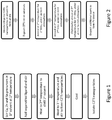
- the process comprises the following steps: stirring the copper, zinc and tin precursors and the organothiol ligand in a first solvent at a first temperature below the boiling point of the first solvent to form a mixture; heating the mixture from the first temperature to a second temperature to distil the first solvent; heating the mixture from the second temperature to a third temperature for a time interval to form the CZTS nanoparticles.
- the process is summarised in Figure 1 .
- Suitable copper precursors include, but are not restricted to, an acetate, chloride, bromide, iodide or acetylacetonate.
- a particularly suitable copper precursor is copper (I) acetate.
- the zinc precursor may include, but is not restricted to, an acetate, chloride, bromide, iodide or acetylacetonate.
- a particularly suitable zinc precursor is zinc (II) acetate.
- the tin precursor may include, but is not restricted to, a tin (IV) chloride solution, fuming tin (IV) chloride or tin (IV) chloride pentahydrate.
- a particularly suitable tin precursor is tin (IV) chloride as a solution in dichloromethane, due to its relative ease and safety in handling. The dichloromethane solvent can be removed by distillation during the nanoparticle synthesis.
- the organothiol compound serves both as the sulphur source and the nanoparticle capping ligand.
- the ligand provides dispersibility or solubility in non-polar organic solvents, allowing the nanoparticles to be processed into an ink that can be printed or coated using conventional techniques. Carbon can be detrimental to device performance, so the ligand must be sufficiently labile that it can be removed, e.g. by evaporation, at a temperature within the device processing protocol. In some embodiments it may be desirable that the boiling point of the ligand is substantially lower than that of elemental sulphur, to prevent loss of sulphur from the CZTS film while evaporating the ligand.
- Suitable labile organothiol ligands include, but are not restricted to, an alkanethiol, alkenethiol or aromatic thiol.
- the organothiol ligand has a boiling point in the range 190 - 300°C.
- An example of a suitable labile organothiol ligand is 1-dodecanethiol, which has a boiling point of 260°C.
- the first solvent which is used to disperse the copper, zinc and tin precursors, is dichloromethane.
- the first temperature, at which the copper, zinc and tin precursors are stirred, must be substantially below the boiling point of the first solvent.
- the first temperature may, for example, be room temperature.
- the second temperature depends on the boiling point of the first solvent.
- a suitable second temperature, or range of temperatures lies between 50 and 55°C.
- the third temperature is greater than 180°C, to avoid the formation of one or more impurity phases. It is important to avoid the formation of impurity phases to achieve a homogeneous melting point, in order to grow large, phase-pure grains during sintering.
- the third temperature lies in the range 200 - 250°C, for example around 240°C.
- the time interval at which the reaction is held at the third temperature may, for example, lie in the range 30 minutes - 3 hours. For instance, the time interval may be around 60 minutes.
- the nanoparticles can be isolated and collected by any method known to those skilled in the art.
- the nanoparticles are isolated via the addition of one or more organic solvents to induce flocculation, followed by centrifugation.
- a suitable combination of organic solvents for the isolation of organothiol-capped CZTS nanoparticles is chloroform and acetone.
- the isolated nanoparticles can be processed to form an absorber layer for a PV device.
- a process for making a Cu 2 ZnSnS 4 absorber layer comprising: depositing an ink on a substrate to form a film, wherein the ink comprises Cu 2 ZnSnS 4 nanoparticles comprising a labile organothiol ligand; and annealing the film at a first temperature less than 300°C, under an inert atmosphere, to remove at least a portion of the labile organothiol ligand from the Cu 2 ZnSnS 4 nanoparticles.
- the method for processing CZTS nanoparticles to form an absorber layer for a PV device is summarised in Figure 2 .
- the method involves: dissolving or dispersing the CZTS nanoparticles in one or more solvents to form an ink; depositing the ink on a substrate; annealing at a first temperature, for a first time interval, under an inert atmosphere to remove the ligand; annealing at a second temperature, for a second time interval, under an inert atmosphere to induce crystallisation of the film; and optionally annealing at a third temperature, for a third time interval, under a selenium-rich and/or sulphur-rich atmosphere. Subsequent layers can then be deposited to form a photovoltaic device.
- the CZTS nanoparticles can be dissolved or dispersed in one or more solvents by any method known to one skilled in the art, including shaking, stirring or ultrasonication.
- the solvent, or solvents are non-polar. Examples include, but are not restricted to, toluene, alkanes ( e.g . hexane), chlorinated solvents e.g. (dichloromethane, chloroform, etc .), ketones (e.g. isophorone), ethers ( e.g. anisole), and terpenes ( e.g. ⁇ -terpinene, limonene, etc .).
- other additives such as binders, rheology modifiers, and the like, may be incorporated into the ink formulation to modify its coating properties.
- the ink can be deposited on a substrate using any method known to one skilled in the art. Examples include, but are not restricted to, spin-coating, slit-coating, drop-casting, doctor blading, and inkjet printing.
- the ink is annealed at a first temperature to remove the solvent, ligand, and other organic components of the ink formulation. This eliminates carbon residues, which can be detrimental to device performance, from the film.
- the first annealing temperature depends on the boiling points of the organic components of the nanoparticle ink. In some embodiments, the first annealing temperature lies in the range 260 - 350°C, for example around 300°C. The first time interval may lie in the range 3 - 10 minutes, for example around 5 minutes. In some embodiments, the first annealing step is conducted under an inert atmosphere.
- the films are annealed at a second temperature to induce crystallisation of the CZTS layer (sintering).
- the second annealing temperature lies in the range 350 - 440°C, for example around 400°C.
- the second time interval may lie in the range 3 - 10 minutes, for example around 5 minutes.
- the sintering step is conducted under an inert atmosphere.
- the ink deposition, first and second annealing steps may be repeated until a desired film thickness is achieved.
- the films may be annealed under a sulphur-rich or selenium-rich atmosphere.
- Suitable sulphurisation sources include H 2 S and elemental sulphur.
- Suitable selenium sources include H 2 Se and elemental Se.
- the third annealing temperature preferably lies in the range 500 - 600°C, more preferably around 550°C.
- the third time interval preferably lies in the range 30 minutes - 3 hours, most preferably around 1 - 2 hours.
- Additional layers can be deposited on top of the CZTS layer to form a PV device.
- Elemental analysis by inductively coupled plasma optical emission spectroscopy gave the following elemental ratios: C 13.49%; H 2.27%; Cu 27.63%; Zn 13.20%; Sn 17.97%; S 18.83%. This gives a stoichiometry of Cu 2.87 Zn 1.33 Sn 1.00 S 3.88 , suggesting that the material is slightly copper and zinc rich.
- the stoichiometry can be tuned by altering the ratios of the metal precursors.
- Figure 3 shows the X-ray diffraction (XRD) pattern for the CZTS nanoparticles (dashed line); the peak positions and intensities are well matched to those of the kesterite crystal structure of CZTS as reported in the literature [ P. Bonazzi et al., Canadian Mineral., 2003, 41, 639 ] (shown and indexed in black). Additional low intensity peaks are seen that are suggestive of a minor wurtzite phase [ X. Lu et al., Chem. Commun., 2011, 47, 3141 ] (shown and indexed in grey).
- XRD X-ray diffraction
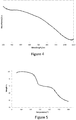
- Figure 4 shows the absorption spectrum (in toluene) of the CZTS nanoparticles.
- the spectrum has a broad absorbance spanning from the ultraviolet to the near-infrared region.
- FIG. 5 shows thermogravimetric analysis (TGA) of the CZTS nanoparticles synthesised in the Examples, showing two steps; the first is likely to be loss of the 1-dodecanethiol ligand capping the surface, suggesting an inorganic content of 90 %. The second step is likely to result from loss of inorganic sulphur (boiling point 444.7°C) from within the nanoparticles; this suggests that annealing temperatures of or below 400°C are desirable for device processing to avoid the loss of sulphur from the film.
- TGA thermogravimetric analysis
Landscapes
- Chemical & Material Sciences (AREA)
- Organic Chemistry (AREA)
- Inorganic Chemistry (AREA)
- Photovoltaic Devices (AREA)
- Powder Metallurgy (AREA)
- Luminescent Compositions (AREA)
Applications Claiming Priority (2)
| Application Number | Priority Date | Filing Date | Title |
|---|---|---|---|
| US201361798084P | 2013-03-15 | 2013-03-15 | |
| PCT/IB2014/001118 WO2014140889A2 (en) | 2013-03-15 | 2014-03-14 | Cu2znsns4 nanoparticles |
Publications (2)
| Publication Number | Publication Date |
|---|---|
| EP2994418A2 EP2994418A2 (en) | 2016-03-16 |
| EP2994418B1 true EP2994418B1 (en) | 2021-02-17 |
Family
ID=51176411
Family Applications (1)
| Application Number | Title | Priority Date | Filing Date |
|---|---|---|---|
| EP14738593.4A Active EP2994418B1 (en) | 2013-03-15 | 2014-03-14 | Cu2znsns4 nanoparticles |
Country Status (7)
| Country | Link |
|---|---|
| US (2) | US9206054B2 (enExample) |
| EP (1) | EP2994418B1 (enExample) |
| JP (2) | JP6138288B2 (enExample) |
| KR (1) | KR101716367B1 (enExample) |
| CN (1) | CN105164047B (enExample) |
| HK (1) | HK1215239A1 (enExample) |
| WO (1) | WO2014140889A2 (enExample) |
Families Citing this family (6)
| Publication number | Priority date | Publication date | Assignee | Title |
|---|---|---|---|---|
| US10453978B2 (en) | 2015-03-12 | 2019-10-22 | International Business Machines Corporation | Single crystalline CZTSSe photovoltaic device |
| CN105226131B (zh) * | 2015-08-24 | 2017-09-29 | 中国工程物理研究院材料研究所 | 一种铜锌锡硫吸收层薄膜的化学合成方法 |
| US9935214B2 (en) | 2015-10-12 | 2018-04-03 | International Business Machines Corporation | Liftoff process for exfoliation of thin film photovoltaic devices and back contact formation |
| CN106629820B (zh) * | 2016-09-09 | 2019-05-24 | 武汉理工大学 | Cu2ZnSnS4纳米晶材料的可控制备方法 |
| JP7365069B2 (ja) * | 2018-08-16 | 2023-10-19 | ノースウェスタン ユニバーシティ | 多元素ヘテロ構造ナノ粒子およびその製造方法 |
| CN113044813B (zh) * | 2019-12-26 | 2022-06-10 | 温州大学 | 一种铜锌锡硒纳米晶及其合成方法 |
Family Cites Families (14)
| Publication number | Priority date | Publication date | Assignee | Title |
|---|---|---|---|---|
| US20110056564A1 (en) * | 2008-05-09 | 2011-03-10 | Korgel Brian A | Nanoparticles and methods of making and using |
| JP5649072B2 (ja) * | 2009-02-27 | 2015-01-07 | 国立大学法人名古屋大学 | 半導体ナノ粒子及びその製法 |
| US20120055554A1 (en) * | 2009-05-21 | 2012-03-08 | E.I. Du Pont De Nemours And Company | Copper zinc tin chalcogenide nanoparticles |
| WO2010138636A2 (en) * | 2009-05-26 | 2010-12-02 | Purdue Research Foundation | Synthesis of multinary chalcogenide nanoparticles comprising cu, zn, sn, s, and se |
| EP2504276A1 (en) * | 2009-11-25 | 2012-10-03 | E. I. du Pont de Nemours and Company | Aqueous process for producing crystalline copper chalcogenide nanoparticles, the nanoparticles so-produced, and inks and coated substrates incorporating the nanoparticles |
| JP2013512306A (ja) * | 2009-11-25 | 2013-04-11 | イー・アイ・デュポン・ドウ・ヌムール・アンド・カンパニー | CZTS/Se前駆体インクとCZTS/Se薄フィルムおよびCZTS/Se系光電池の製造方法 |
| CN101830445B (zh) * | 2009-12-15 | 2014-12-10 | 河南大学 | 一种以乙酰丙酮盐为原料合成无机纳米晶的方法 |
| KR101144738B1 (ko) * | 2009-12-28 | 2012-05-24 | 재단법인대구경북과학기술원 | 박막형 태양전지의 제조방법 |
| US20120067408A1 (en) * | 2010-09-16 | 2012-03-22 | Solexant Corp. | Sintered CZTS Nanoparticle Solar Cells |
| KR20140015280A (ko) * | 2010-11-22 | 2014-02-06 | 이 아이 듀폰 디 네모아 앤드 캄파니 | 반도체 잉크, 피막, 코팅된 기재 및 제조방법 |
| US20130233202A1 (en) * | 2010-12-03 | 2013-09-12 | Ei Du Pont De Nemours And Company | Inks and processes for preparing copper indium gallium sulfide/selenide coatings and films |
| CN102108540B (zh) * | 2010-12-27 | 2012-07-25 | 中国科学院长春光学精密机械与物理研究所 | 合成单分散多元化合物纳米晶的方法 |
| JP2012250889A (ja) * | 2011-06-06 | 2012-12-20 | Toyota Motor Corp | 半導体粒子及びその製造方法 |
| JP5884945B2 (ja) * | 2013-03-07 | 2016-03-15 | 株式会社村田製作所 | 化合物半導体超微粒子、超微粒子薄膜及び光電変換デバイス |
-
2014
- 2014-03-14 CN CN201480015872.3A patent/CN105164047B/zh active Active
- 2014-03-14 WO PCT/IB2014/001118 patent/WO2014140889A2/en not_active Ceased
- 2014-03-14 KR KR1020157029348A patent/KR101716367B1/ko active Active
- 2014-03-14 EP EP14738593.4A patent/EP2994418B1/en active Active
- 2014-03-14 HK HK16103114.7A patent/HK1215239A1/zh unknown
- 2014-03-14 JP JP2015562392A patent/JP6138288B2/ja active Active
- 2014-03-14 US US14/210,727 patent/US9206054B2/en active Active
-
2015
- 2015-09-02 US US14/842,909 patent/US9359222B2/en active Active
-
2017
- 2017-04-24 JP JP2017085335A patent/JP6623192B2/ja not_active Expired - Fee Related
Non-Patent Citations (1)
| Title |
|---|
| AJAY SINGH ET AL: "Colloidal Synthesis of Wurtzite Cu 2 ZnSnS 4 Nanorods and Their Perpendicular Assembly", JOURNAL OF THE AMERICAN CHEMICAL SOCIETY, vol. 134, no. 6, 15 February 2012 (2012-02-15), pages 2910 - 2913, XP055145184, ISSN: 0002-7863, DOI: 10.1021/ja2112146 * |
Also Published As
| Publication number | Publication date |
|---|---|
| CN105164047A (zh) | 2015-12-16 |
| JP6623192B2 (ja) | 2019-12-18 |
| HK1215239A1 (zh) | 2016-08-19 |
| JP2017206431A (ja) | 2017-11-24 |
| JP6138288B2 (ja) | 2017-05-31 |
| KR20150126966A (ko) | 2015-11-13 |
| US20140273337A1 (en) | 2014-09-18 |
| WO2014140889A3 (en) | 2015-01-08 |
| JP2016515990A (ja) | 2016-06-02 |
| CN105164047B (zh) | 2019-03-15 |
| US20150376026A1 (en) | 2015-12-31 |
| WO2014140889A2 (en) | 2014-09-18 |
| EP2994418A2 (en) | 2016-03-16 |
| US9359222B2 (en) | 2016-06-07 |
| US9206054B2 (en) | 2015-12-08 |
| KR101716367B1 (ko) | 2017-03-14 |
Similar Documents
| Publication | Publication Date | Title |
|---|---|---|
| US10756221B2 (en) | Cu2XSnY4 nanoparticles | |
| US9359222B2 (en) | Methods for preparing Cu2ZnSnS4 nanoparticles for use in thin film photovoltaic cells | |
| EP2870621B1 (en) | Group 13 selenide nanoparticles | |
| US10170651B2 (en) | Metal-doped cu(In,Ga) (S,Se)2 nanoparticles | |
| JP5756899B2 (ja) | カルコパイライト構造を有する化合物の製造方法 | |
| US20180248057A1 (en) | Preparation of Copper-Rich Copper Indium (Gallium) Diselenide/Disulphide Nanoparticles | |
| TWI510437B (zh) | A method for producing a compound having a chalcopyrite structure |
Legal Events
| Date | Code | Title | Description |
|---|---|---|---|
| PUAI | Public reference made under article 153(3) epc to a published international application that has entered the european phase |
Free format text: ORIGINAL CODE: 0009012 |
|
| 17P | Request for examination filed |
Effective date: 20150825 |
|
| AK | Designated contracting states |
Kind code of ref document: A2 Designated state(s): AL AT BE BG CH CY CZ DE DK EE ES FI FR GB GR HR HU IE IS IT LI LT LU LV MC MK MT NL NO PL PT RO RS SE SI SK SM TR |
|
| AX | Request for extension of the european patent |
Extension state: BA ME |
|
| DAX | Request for extension of the european patent (deleted) | ||
| REG | Reference to a national code |
Ref country code: HK Ref legal event code: DE Ref document number: 1215239 Country of ref document: HK |
|
| 17Q | First examination report despatched |
Effective date: 20160919 |
|
| STAA | Information on the status of an ep patent application or granted ep patent |
Free format text: STATUS: EXAMINATION IS IN PROGRESS |
|
| RIN1 | Information on inventor provided before grant (corrected) |
Inventor name: HARRIS, JAMES Inventor name: PICKETT, NIGEL Inventor name: MASALA, OMBRETTA Inventor name: GRESTY, NATHALIE |
|
| GRAP | Despatch of communication of intention to grant a patent |
Free format text: ORIGINAL CODE: EPIDOSNIGR1 |
|
| STAA | Information on the status of an ep patent application or granted ep patent |
Free format text: STATUS: GRANT OF PATENT IS INTENDED |
|
| INTG | Intention to grant announced |
Effective date: 20201126 |
|
| RIN1 | Information on inventor provided before grant (corrected) |
Inventor name: PICKETT, NIGEL Inventor name: HARRIS, JAMES Inventor name: GRESTY, NATHALIE Inventor name: MASALA, OMBRETTA |
|
| GRAS | Grant fee paid |
Free format text: ORIGINAL CODE: EPIDOSNIGR3 |
|
| GRAA | (expected) grant |
Free format text: ORIGINAL CODE: 0009210 |
|
| STAA | Information on the status of an ep patent application or granted ep patent |
Free format text: STATUS: THE PATENT HAS BEEN GRANTED |
|
| AK | Designated contracting states |
Kind code of ref document: B1 Designated state(s): AL AT BE BG CH CY CZ DE DK EE ES FI FR GB GR HR HU IE IS IT LI LT LU LV MC MK MT NL NO PL PT RO RS SE SI SK SM TR |
|
| REG | Reference to a national code |
Ref country code: GB Ref legal event code: FG4D |
|
| REG | Reference to a national code |
Ref country code: CH Ref legal event code: EP |
|
| REG | Reference to a national code |
Ref country code: DE Ref legal event code: R096 Ref document number: 602014074838 Country of ref document: DE |
|
| REG | Reference to a national code |
Ref country code: AT Ref legal event code: REF Ref document number: 1361221 Country of ref document: AT Kind code of ref document: T Effective date: 20210315 |
|
| REG | Reference to a national code |
Ref country code: IE Ref legal event code: FG4D |
|
| REG | Reference to a national code |
Ref country code: NL Ref legal event code: FP |
|
| REG | Reference to a national code |
Ref country code: LT Ref legal event code: MG9D |
|
| PG25 | Lapsed in a contracting state [announced via postgrant information from national office to epo] |
Ref country code: FI Free format text: LAPSE BECAUSE OF FAILURE TO SUBMIT A TRANSLATION OF THE DESCRIPTION OR TO PAY THE FEE WITHIN THE PRESCRIBED TIME-LIMIT Effective date: 20210217 Ref country code: GR Free format text: LAPSE BECAUSE OF FAILURE TO SUBMIT A TRANSLATION OF THE DESCRIPTION OR TO PAY THE FEE WITHIN THE PRESCRIBED TIME-LIMIT Effective date: 20210518 Ref country code: HR Free format text: LAPSE BECAUSE OF FAILURE TO SUBMIT A TRANSLATION OF THE DESCRIPTION OR TO PAY THE FEE WITHIN THE PRESCRIBED TIME-LIMIT Effective date: 20210217 Ref country code: PT Free format text: LAPSE BECAUSE OF FAILURE TO SUBMIT A TRANSLATION OF THE DESCRIPTION OR TO PAY THE FEE WITHIN THE PRESCRIBED TIME-LIMIT Effective date: 20210617 Ref country code: LT Free format text: LAPSE BECAUSE OF FAILURE TO SUBMIT A TRANSLATION OF THE DESCRIPTION OR TO PAY THE FEE WITHIN THE PRESCRIBED TIME-LIMIT Effective date: 20210217 Ref country code: BG Free format text: LAPSE BECAUSE OF FAILURE TO SUBMIT A TRANSLATION OF THE DESCRIPTION OR TO PAY THE FEE WITHIN THE PRESCRIBED TIME-LIMIT Effective date: 20210517 Ref country code: NO Free format text: LAPSE BECAUSE OF FAILURE TO SUBMIT A TRANSLATION OF THE DESCRIPTION OR TO PAY THE FEE WITHIN THE PRESCRIBED TIME-LIMIT Effective date: 20210517 |
|
| REG | Reference to a national code |
Ref country code: AT Ref legal event code: MK05 Ref document number: 1361221 Country of ref document: AT Kind code of ref document: T Effective date: 20210217 |
|
| PG25 | Lapsed in a contracting state [announced via postgrant information from national office to epo] |
Ref country code: PL Free format text: LAPSE BECAUSE OF FAILURE TO SUBMIT A TRANSLATION OF THE DESCRIPTION OR TO PAY THE FEE WITHIN THE PRESCRIBED TIME-LIMIT Effective date: 20210217 Ref country code: LV Free format text: LAPSE BECAUSE OF FAILURE TO SUBMIT A TRANSLATION OF THE DESCRIPTION OR TO PAY THE FEE WITHIN THE PRESCRIBED TIME-LIMIT Effective date: 20210217 Ref country code: RS Free format text: LAPSE BECAUSE OF FAILURE TO SUBMIT A TRANSLATION OF THE DESCRIPTION OR TO PAY THE FEE WITHIN THE PRESCRIBED TIME-LIMIT Effective date: 20210217 Ref country code: SE Free format text: LAPSE BECAUSE OF FAILURE TO SUBMIT A TRANSLATION OF THE DESCRIPTION OR TO PAY THE FEE WITHIN THE PRESCRIBED TIME-LIMIT Effective date: 20210217 |
|
| PG25 | Lapsed in a contracting state [announced via postgrant information from national office to epo] |
Ref country code: IS Free format text: LAPSE BECAUSE OF FAILURE TO SUBMIT A TRANSLATION OF THE DESCRIPTION OR TO PAY THE FEE WITHIN THE PRESCRIBED TIME-LIMIT Effective date: 20210617 |
|
| PG25 | Lapsed in a contracting state [announced via postgrant information from national office to epo] |
Ref country code: SM Free format text: LAPSE BECAUSE OF FAILURE TO SUBMIT A TRANSLATION OF THE DESCRIPTION OR TO PAY THE FEE WITHIN THE PRESCRIBED TIME-LIMIT Effective date: 20210217 Ref country code: CZ Free format text: LAPSE BECAUSE OF FAILURE TO SUBMIT A TRANSLATION OF THE DESCRIPTION OR TO PAY THE FEE WITHIN THE PRESCRIBED TIME-LIMIT Effective date: 20210217 Ref country code: EE Free format text: LAPSE BECAUSE OF FAILURE TO SUBMIT A TRANSLATION OF THE DESCRIPTION OR TO PAY THE FEE WITHIN THE PRESCRIBED TIME-LIMIT Effective date: 20210217 Ref country code: AT Free format text: LAPSE BECAUSE OF FAILURE TO SUBMIT A TRANSLATION OF THE DESCRIPTION OR TO PAY THE FEE WITHIN THE PRESCRIBED TIME-LIMIT Effective date: 20210217 |
|
| REG | Reference to a national code |
Ref country code: CH Ref legal event code: PL |
|
| REG | Reference to a national code |
Ref country code: DE Ref legal event code: R097 Ref document number: 602014074838 Country of ref document: DE |
|
| PG25 | Lapsed in a contracting state [announced via postgrant information from national office to epo] |
Ref country code: SK Free format text: LAPSE BECAUSE OF FAILURE TO SUBMIT A TRANSLATION OF THE DESCRIPTION OR TO PAY THE FEE WITHIN THE PRESCRIBED TIME-LIMIT Effective date: 20210217 Ref country code: RO Free format text: LAPSE BECAUSE OF FAILURE TO SUBMIT A TRANSLATION OF THE DESCRIPTION OR TO PAY THE FEE WITHIN THE PRESCRIBED TIME-LIMIT Effective date: 20210217 Ref country code: ES Free format text: LAPSE BECAUSE OF FAILURE TO SUBMIT A TRANSLATION OF THE DESCRIPTION OR TO PAY THE FEE WITHIN THE PRESCRIBED TIME-LIMIT Effective date: 20210217 Ref country code: DK Free format text: LAPSE BECAUSE OF FAILURE TO SUBMIT A TRANSLATION OF THE DESCRIPTION OR TO PAY THE FEE WITHIN THE PRESCRIBED TIME-LIMIT Effective date: 20210217 Ref country code: MC Free format text: LAPSE BECAUSE OF FAILURE TO SUBMIT A TRANSLATION OF THE DESCRIPTION OR TO PAY THE FEE WITHIN THE PRESCRIBED TIME-LIMIT Effective date: 20210217 |
|
| REG | Reference to a national code |
Ref country code: BE Ref legal event code: MM Effective date: 20210331 |
|
| PLBE | No opposition filed within time limit |
Free format text: ORIGINAL CODE: 0009261 |
|
| STAA | Information on the status of an ep patent application or granted ep patent |
Free format text: STATUS: NO OPPOSITION FILED WITHIN TIME LIMIT |
|
| 26N | No opposition filed |
Effective date: 20211118 |
|
| PG25 | Lapsed in a contracting state [announced via postgrant information from national office to epo] |
Ref country code: AL Free format text: LAPSE BECAUSE OF FAILURE TO SUBMIT A TRANSLATION OF THE DESCRIPTION OR TO PAY THE FEE WITHIN THE PRESCRIBED TIME-LIMIT Effective date: 20210217 Ref country code: CH Free format text: LAPSE BECAUSE OF NON-PAYMENT OF DUE FEES Effective date: 20210331 Ref country code: LI Free format text: LAPSE BECAUSE OF NON-PAYMENT OF DUE FEES Effective date: 20210331 Ref country code: LU Free format text: LAPSE BECAUSE OF NON-PAYMENT OF DUE FEES Effective date: 20210314 Ref country code: IE Free format text: LAPSE BECAUSE OF NON-PAYMENT OF DUE FEES Effective date: 20210314 |
|
| PG25 | Lapsed in a contracting state [announced via postgrant information from national office to epo] |
Ref country code: SI Free format text: LAPSE BECAUSE OF FAILURE TO SUBMIT A TRANSLATION OF THE DESCRIPTION OR TO PAY THE FEE WITHIN THE PRESCRIBED TIME-LIMIT Effective date: 20210217 |
|
| PG25 | Lapsed in a contracting state [announced via postgrant information from national office to epo] |
Ref country code: IT Free format text: LAPSE BECAUSE OF FAILURE TO SUBMIT A TRANSLATION OF THE DESCRIPTION OR TO PAY THE FEE WITHIN THE PRESCRIBED TIME-LIMIT Effective date: 20210217 |
|
| PG25 | Lapsed in a contracting state [announced via postgrant information from national office to epo] |
Ref country code: IS Free format text: LAPSE BECAUSE OF FAILURE TO SUBMIT A TRANSLATION OF THE DESCRIPTION OR TO PAY THE FEE WITHIN THE PRESCRIBED TIME-LIMIT Effective date: 20210617 |
|
| PG25 | Lapsed in a contracting state [announced via postgrant information from national office to epo] |
Ref country code: BE Free format text: LAPSE BECAUSE OF NON-PAYMENT OF DUE FEES Effective date: 20210331 |
|
| REG | Reference to a national code |
Ref country code: HK Ref legal event code: WD Ref document number: 1215239 Country of ref document: HK |
|
| PG25 | Lapsed in a contracting state [announced via postgrant information from national office to epo] |
Ref country code: HU Free format text: LAPSE BECAUSE OF FAILURE TO SUBMIT A TRANSLATION OF THE DESCRIPTION OR TO PAY THE FEE WITHIN THE PRESCRIBED TIME-LIMIT; INVALID AB INITIO Effective date: 20140314 |
|
| PG25 | Lapsed in a contracting state [announced via postgrant information from national office to epo] |
Ref country code: CY Free format text: LAPSE BECAUSE OF FAILURE TO SUBMIT A TRANSLATION OF THE DESCRIPTION OR TO PAY THE FEE WITHIN THE PRESCRIBED TIME-LIMIT Effective date: 20210217 |
|
| P01 | Opt-out of the competence of the unified patent court (upc) registered |
Effective date: 20230525 |
|
| PG25 | Lapsed in a contracting state [announced via postgrant information from national office to epo] |
Ref country code: MK Free format text: LAPSE BECAUSE OF FAILURE TO SUBMIT A TRANSLATION OF THE DESCRIPTION OR TO PAY THE FEE WITHIN THE PRESCRIBED TIME-LIMIT Effective date: 20210217 |
|
| PG25 | Lapsed in a contracting state [announced via postgrant information from national office to epo] |
Ref country code: MT Free format text: LAPSE BECAUSE OF FAILURE TO SUBMIT A TRANSLATION OF THE DESCRIPTION OR TO PAY THE FEE WITHIN THE PRESCRIBED TIME-LIMIT Effective date: 20210217 |
|
| PGFP | Annual fee paid to national office [announced via postgrant information from national office to epo] |
Ref country code: FR Payment date: 20241231 Year of fee payment: 12 |
|
| PGFP | Annual fee paid to national office [announced via postgrant information from national office to epo] |
Ref country code: NL Payment date: 20250108 Year of fee payment: 12 |
|
| PGFP | Annual fee paid to national office [announced via postgrant information from national office to epo] |
Ref country code: DE Payment date: 20241231 Year of fee payment: 12 |
|
| PGFP | Annual fee paid to national office [announced via postgrant information from national office to epo] |
Ref country code: GB Payment date: 20250102 Year of fee payment: 12 |
|
| PG25 | Lapsed in a contracting state [announced via postgrant information from national office to epo] |
Ref country code: TR Free format text: LAPSE BECAUSE OF FAILURE TO SUBMIT A TRANSLATION OF THE DESCRIPTION OR TO PAY THE FEE WITHIN THE PRESCRIBED TIME-LIMIT Effective date: 20210217 |