EP2993695A1 - Semi-floating gate device and manufacturing method therefor - Google Patents
Semi-floating gate device and manufacturing method therefor Download PDFInfo
- Publication number
- EP2993695A1 EP2993695A1 EP14791834.6A EP14791834A EP2993695A1 EP 2993695 A1 EP2993695 A1 EP 2993695A1 EP 14791834 A EP14791834 A EP 14791834A EP 2993695 A1 EP2993695 A1 EP 2993695A1
- Authority
- EP
- European Patent Office
- Prior art keywords
- layer
- region
- gate
- floating
- floating gate
- Prior art date
- Legal status (The legal status is an assumption and is not a legal conclusion. Google has not performed a legal analysis and makes no representation as to the accuracy of the status listed.)
- Withdrawn
Links
Images


Classifications
-
- H—ELECTRICITY
- H10—SEMICONDUCTOR DEVICES; ELECTRIC SOLID-STATE DEVICES NOT OTHERWISE PROVIDED FOR
- H10D—INORGANIC ELECTRIC SEMICONDUCTOR DEVICES
- H10D30/00—Field-effect transistors [FET]
- H10D30/60—Insulated-gate field-effect transistors [IGFET]
- H10D30/68—Floating-gate IGFETs
-
- H—ELECTRICITY
- H10—SEMICONDUCTOR DEVICES; ELECTRIC SOLID-STATE DEVICES NOT OTHERWISE PROVIDED FOR
- H10B—ELECTRONIC MEMORY DEVICES
- H10B41/00—Electrically erasable-and-programmable ROM [EEPROM] devices comprising floating gates
- H10B41/20—Electrically erasable-and-programmable ROM [EEPROM] devices comprising floating gates characterised by three-dimensional [3D] arrangements, e.g. with cells on different height levels
- H10B41/23—Electrically erasable-and-programmable ROM [EEPROM] devices comprising floating gates characterised by three-dimensional [3D] arrangements, e.g. with cells on different height levels with source and drain on different levels, e.g. with sloping channels
-
- H—ELECTRICITY
- H10—SEMICONDUCTOR DEVICES; ELECTRIC SOLID-STATE DEVICES NOT OTHERWISE PROVIDED FOR
- H10B—ELECTRONIC MEMORY DEVICES
- H10B41/00—Electrically erasable-and-programmable ROM [EEPROM] devices comprising floating gates
- H10B41/20—Electrically erasable-and-programmable ROM [EEPROM] devices comprising floating gates characterised by three-dimensional [3D] arrangements, e.g. with cells on different height levels
- H10B41/23—Electrically erasable-and-programmable ROM [EEPROM] devices comprising floating gates characterised by three-dimensional [3D] arrangements, e.g. with cells on different height levels with source and drain on different levels, e.g. with sloping channels
- H10B41/27—Electrically erasable-and-programmable ROM [EEPROM] devices comprising floating gates characterised by three-dimensional [3D] arrangements, e.g. with cells on different height levels with source and drain on different levels, e.g. with sloping channels the channels comprising vertical portions, e.g. U-shaped channels
-
- H—ELECTRICITY
- H10—SEMICONDUCTOR DEVICES; ELECTRIC SOLID-STATE DEVICES NOT OTHERWISE PROVIDED FOR
- H10B—ELECTRONIC MEMORY DEVICES
- H10B41/00—Electrically erasable-and-programmable ROM [EEPROM] devices comprising floating gates
- H10B41/30—Electrically erasable-and-programmable ROM [EEPROM] devices comprising floating gates characterised by the memory core region
-
- H—ELECTRICITY
- H10—SEMICONDUCTOR DEVICES; ELECTRIC SOLID-STATE DEVICES NOT OTHERWISE PROVIDED FOR
- H10D—INORGANIC ELECTRIC SEMICONDUCTOR DEVICES
- H10D30/00—Field-effect transistors [FET]
- H10D30/01—Manufacture or treatment
- H10D30/021—Manufacture or treatment of FETs having insulated gates [IGFET]
- H10D30/025—Manufacture or treatment of FETs having insulated gates [IGFET] of vertical IGFETs
-
- H—ELECTRICITY
- H10—SEMICONDUCTOR DEVICES; ELECTRIC SOLID-STATE DEVICES NOT OTHERWISE PROVIDED FOR
- H10D—INORGANIC ELECTRIC SEMICONDUCTOR DEVICES
- H10D30/00—Field-effect transistors [FET]
- H10D30/01—Manufacture or treatment
- H10D30/021—Manufacture or treatment of FETs having insulated gates [IGFET]
- H10D30/0411—Manufacture or treatment of FETs having insulated gates [IGFET] of FETs having floating gates
-
- H—ELECTRICITY
- H10—SEMICONDUCTOR DEVICES; ELECTRIC SOLID-STATE DEVICES NOT OTHERWISE PROVIDED FOR
- H10D—INORGANIC ELECTRIC SEMICONDUCTOR DEVICES
- H10D30/00—Field-effect transistors [FET]
- H10D30/60—Insulated-gate field-effect transistors [IGFET]
- H10D30/63—Vertical IGFETs
-
- H—ELECTRICITY
- H10—SEMICONDUCTOR DEVICES; ELECTRIC SOLID-STATE DEVICES NOT OTHERWISE PROVIDED FOR
- H10D—INORGANIC ELECTRIC SEMICONDUCTOR DEVICES
- H10D30/00—Field-effect transistors [FET]
- H10D30/60—Insulated-gate field-effect transistors [IGFET]
- H10D30/68—Floating-gate IGFETs
- H10D30/689—Vertical floating-gate IGFETs
-
- H—ELECTRICITY
- H10—SEMICONDUCTOR DEVICES; ELECTRIC SOLID-STATE DEVICES NOT OTHERWISE PROVIDED FOR
- H10D—INORGANIC ELECTRIC SEMICONDUCTOR DEVICES
- H10D30/00—Field-effect transistors [FET]
- H10D30/60—Insulated-gate field-effect transistors [IGFET]
- H10D30/68—Floating-gate IGFETs
- H10D30/6891—Floating-gate IGFETs characterised by the shapes, relative sizes or dispositions of the floating gate electrode
-
- H—ELECTRICITY
- H10—SEMICONDUCTOR DEVICES; ELECTRIC SOLID-STATE DEVICES NOT OTHERWISE PROVIDED FOR
- H10D—INORGANIC ELECTRIC SEMICONDUCTOR DEVICES
- H10D30/00—Field-effect transistors [FET]
- H10D30/60—Insulated-gate field-effect transistors [IGFET]
- H10D30/68—Floating-gate IGFETs
- H10D30/6891—Floating-gate IGFETs characterised by the shapes, relative sizes or dispositions of the floating gate electrode
- H10D30/6894—Floating-gate IGFETs characterised by the shapes, relative sizes or dispositions of the floating gate electrode having one gate at least partly in a trench
-
- H—ELECTRICITY
- H10—SEMICONDUCTOR DEVICES; ELECTRIC SOLID-STATE DEVICES NOT OTHERWISE PROVIDED FOR
- H10D—INORGANIC ELECTRIC SEMICONDUCTOR DEVICES
- H10D62/00—Semiconductor bodies, or regions thereof, of devices having potential barriers
- H10D62/10—Shapes, relative sizes or dispositions of the regions of the semiconductor bodies; Shapes of the semiconductor bodies
- H10D62/13—Semiconductor regions connected to electrodes carrying current to be rectified, amplified or switched, e.g. source or drain regions
- H10D62/149—Source or drain regions of field-effect devices
- H10D62/151—Source or drain regions of field-effect devices of IGFETs
-
- H—ELECTRICITY
- H10—SEMICONDUCTOR DEVICES; ELECTRIC SOLID-STATE DEVICES NOT OTHERWISE PROVIDED FOR
- H10D—INORGANIC ELECTRIC SEMICONDUCTOR DEVICES
- H10D62/00—Semiconductor bodies, or regions thereof, of devices having potential barriers
- H10D62/10—Shapes, relative sizes or dispositions of the regions of the semiconductor bodies; Shapes of the semiconductor bodies
- H10D62/17—Semiconductor regions connected to electrodes not carrying current to be rectified, amplified or switched, e.g. channel regions
- H10D62/213—Channel regions of field-effect devices
- H10D62/221—Channel regions of field-effect devices of FETs
- H10D62/235—Channel regions of field-effect devices of FETs of IGFETs
- H10D62/292—Non-planar channels of IGFETs
-
- H—ELECTRICITY
- H10—SEMICONDUCTOR DEVICES; ELECTRIC SOLID-STATE DEVICES NOT OTHERWISE PROVIDED FOR
- H10D—INORGANIC ELECTRIC SEMICONDUCTOR DEVICES
- H10D64/00—Electrodes of devices having potential barriers
- H10D64/01—Manufacture or treatment
- H10D64/011—Manufacture or treatment of electrodes ohmically coupled to a semiconductor
- H10D64/0111—Manufacture or treatment of electrodes ohmically coupled to a semiconductor to Group IV semiconductors
- H10D64/0113—Manufacture or treatment of electrodes ohmically coupled to a semiconductor to Group IV semiconductors the conductive layers comprising highly doped semiconductor materials, e.g. polysilicon layers or amorphous silicon layers
-
- H—ELECTRICITY
- H10—SEMICONDUCTOR DEVICES; ELECTRIC SOLID-STATE DEVICES NOT OTHERWISE PROVIDED FOR
- H10D—INORGANIC ELECTRIC SEMICONDUCTOR DEVICES
- H10D64/00—Electrodes of devices having potential barriers
- H10D64/01—Manufacture or treatment
- H10D64/031—Manufacture or treatment of data-storage electrodes
- H10D64/035—Manufacture or treatment of data-storage electrodes comprising conductor-insulator-conductor-insulator-semiconductor structures
-
- H—ELECTRICITY
- H10—SEMICONDUCTOR DEVICES; ELECTRIC SOLID-STATE DEVICES NOT OTHERWISE PROVIDED FOR
- H10D—INORGANIC ELECTRIC SEMICONDUCTOR DEVICES
- H10D64/00—Electrodes of devices having potential barriers
- H10D64/20—Electrodes characterised by their shapes, relative sizes or dispositions
-
- H—ELECTRICITY
- H10—SEMICONDUCTOR DEVICES; ELECTRIC SOLID-STATE DEVICES NOT OTHERWISE PROVIDED FOR
- H10D—INORGANIC ELECTRIC SEMICONDUCTOR DEVICES
- H10D64/00—Electrodes of devices having potential barriers
- H10D64/60—Electrodes characterised by their materials
- H10D64/66—Electrodes having a conductor capacitively coupled to a semiconductor by an insulator, e.g. MIS electrodes
- H10D64/661—Electrodes having a conductor capacitively coupled to a semiconductor by an insulator, e.g. MIS electrodes the conductor comprising a layer of silicon contacting the insulator, e.g. polysilicon having vertical doping variation
-
- H—ELECTRICITY
- H10—SEMICONDUCTOR DEVICES; ELECTRIC SOLID-STATE DEVICES NOT OTHERWISE PROVIDED FOR
- H10D—INORGANIC ELECTRIC SEMICONDUCTOR DEVICES
- H10D8/00—Diodes
-
- H—ELECTRICITY
- H10—SEMICONDUCTOR DEVICES; ELECTRIC SOLID-STATE DEVICES NOT OTHERWISE PROVIDED FOR
- H10D—INORGANIC ELECTRIC SEMICONDUCTOR DEVICES
- H10D84/00—Integrated devices formed in or on semiconductor substrates that comprise only semiconducting layers, e.g. on Si wafers or on GaAs-on-Si wafers
- H10D84/80—Integrated devices formed in or on semiconductor substrates that comprise only semiconducting layers, e.g. on Si wafers or on GaAs-on-Si wafers characterised by the integration of at least one component covered by groups H10D12/00 or H10D30/00, e.g. integration of IGFETs
- H10D84/811—Combinations of field-effect devices and one or more diodes, capacitors or resistors
-
- H—ELECTRICITY
- H10—SEMICONDUCTOR DEVICES; ELECTRIC SOLID-STATE DEVICES NOT OTHERWISE PROVIDED FOR
- H10P—GENERIC PROCESSES OR APPARATUS FOR THE MANUFACTURE OR TREATMENT OF DEVICES COVERED BY CLASS H10
- H10P30/00—Ion implantation into wafers, substrates or parts of devices
- H10P30/20—Ion implantation into wafers, substrates or parts of devices into semiconductor materials, e.g. for doping
-
- H—ELECTRICITY
- H10—SEMICONDUCTOR DEVICES; ELECTRIC SOLID-STATE DEVICES NOT OTHERWISE PROVIDED FOR
- H10P—GENERIC PROCESSES OR APPARATUS FOR THE MANUFACTURE OR TREATMENT OF DEVICES COVERED BY CLASS H10
- H10P50/00—Etching of wafers, substrates or parts of devices
- H10P50/60—Wet etching
- H10P50/64—Wet etching of semiconductor materials
- H10P50/642—Chemical etching
-
- H—ELECTRICITY
- H10—SEMICONDUCTOR DEVICES; ELECTRIC SOLID-STATE DEVICES NOT OTHERWISE PROVIDED FOR
- H10P—GENERIC PROCESSES OR APPARATUS FOR THE MANUFACTURE OR TREATMENT OF DEVICES COVERED BY CLASS H10
- H10P50/00—Etching of wafers, substrates or parts of devices
- H10P50/69—Etching of wafers, substrates or parts of devices using masks for semiconductor materials
- H10P50/691—Etching of wafers, substrates or parts of devices using masks for semiconductor materials for Group V materials or Group III-V materials
- H10P50/693—Etching of wafers, substrates or parts of devices using masks for semiconductor materials for Group V materials or Group III-V materials characterised by their size, orientation, disposition, behaviour or shape, in horizontal or vertical plane
- H10P50/694—Etching of wafers, substrates or parts of devices using masks for semiconductor materials for Group V materials or Group III-V materials characterised by their size, orientation, disposition, behaviour or shape, in horizontal or vertical plane characterised by their behaviour during the process, e.g. soluble masks or redeposited masks
-
- H—ELECTRICITY
- H10—SEMICONDUCTOR DEVICES; ELECTRIC SOLID-STATE DEVICES NOT OTHERWISE PROVIDED FOR
- H10P—GENERIC PROCESSES OR APPARATUS FOR THE MANUFACTURE OR TREATMENT OF DEVICES COVERED BY CLASS H10
- H10P50/00—Etching of wafers, substrates or parts of devices
- H10P50/69—Etching of wafers, substrates or parts of devices using masks for semiconductor materials
- H10P50/691—Etching of wafers, substrates or parts of devices using masks for semiconductor materials for Group V materials or Group III-V materials
- H10P50/693—Etching of wafers, substrates or parts of devices using masks for semiconductor materials for Group V materials or Group III-V materials characterised by their size, orientation, disposition, behaviour or shape, in horizontal or vertical plane
- H10P50/695—Etching of wafers, substrates or parts of devices using masks for semiconductor materials for Group V materials or Group III-V materials characterised by their size, orientation, disposition, behaviour or shape, in horizontal or vertical plane characterised by the process involved to create the mask, e.g. lift-off masks or sidewalls or to modify the mask
-
- H—ELECTRICITY
- H10—SEMICONDUCTOR DEVICES; ELECTRIC SOLID-STATE DEVICES NOT OTHERWISE PROVIDED FOR
- H10D—INORGANIC ELECTRIC SEMICONDUCTOR DEVICES
- H10D12/00—Bipolar devices controlled by the field effect, e.g. insulated-gate bipolar transistors [IGBT]
- H10D12/01—Manufacture or treatment
- H10D12/021—Manufacture or treatment of gated diodes, e.g. field-controlled diodes [FCD]
-
- H—ELECTRICITY
- H10—SEMICONDUCTOR DEVICES; ELECTRIC SOLID-STATE DEVICES NOT OTHERWISE PROVIDED FOR
- H10D—INORGANIC ELECTRIC SEMICONDUCTOR DEVICES
- H10D12/00—Bipolar devices controlled by the field effect, e.g. insulated-gate bipolar transistors [IGBT]
- H10D12/211—Gated diodes
Definitions
- the disclosure belonging to the technological field of semiconductor memory relates to a semi-floating-gate device and its manufacturing method, and more especially, to a semi-floating-gate device with perpendicular channel region and its manufacturing method.
- SRAM static random access memory
- DRAM dynamic random access memory
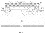
- FIG. 1 shows a planar channeling semiconductor device, comprising: a source region 501 and a drain region 502 with the opposite doping type formed in the semiconductor substrate which can be made of monocrystalline silicon, polysilicon or silicon on insulator.
- a channel region 601 of the device is formed between the source region 501 and the drain region 502, wherein the channel region 601 is an inversion layer formed in the semiconductor substrate 500 when the semiconductor device works.
- the doping region 509 with a high doping concentration is formed in source region 501, and the doping region 510 with a high doping concentration is formed in drain region 502, wherein the doping type of the doping region 509 and the doping region 510 is same to that of the source region 501 and drain region 502.
- a first layer of insulation film 503 is formed above the source region 501, the channel region 601 and the drain region 502, and a floating gate opening region 504 is formed in the first layer of insulation film 503 on the drain region 502.
- a floating gate 505 used as a charge storage node is formed above the first layer of insulation film 503 and covers the channel region 601 and the floating gate opening region 504.
- the floating gate 505 has the doping type opposite to that of the drain region 502. The doped impurities in the floating gate 505 can be diffused into the drain region 502 through the floating gate opening region 504.
- a diffusion region 602 is formed due to the spreading of the impurities diffusion of the floating gate 505.Thus a p-n junction diode is formed between the floating gate 505 and the drain region 502 through the floating gate opening region 504 blew the floating gate 505.
- a second layer of insulation film 506 is formed due to covering the floating gate 505 and the p-n junction diode structure.
- a control gate 507 above the second layer of insulation film 506 is formed due to covering and surrounding the floating gate 505 of the gate of the device 508 are formed on both side of the control gate 507.
- the semiconductor device further comprises the contactor of the source region 511, the contactor of the control gate 507, the contactor of the drain region 513 and the contactor of the semiconductor substrate 514 made of conducting materials, that are used to connect the source region 501, the control gate 507, the drain region 502 and the semiconductor substrate 500 with the external electrode.
- the planar channeling semiconductor device needs longer channel length. But the unit area of semiconductor device will be bigger, and the chip density will be reduced. It will hinder the further development of chips towards miniature direction.
- the disclosure aims at providing a semi-floating-gate device with perpendicular channel region so as to reduce the unit area of semiconductor memory and raise the density of chip.
- the disclosure provides a semi-floating-gate device with perpendicular channel region.
- the floating gate is half-floating, because the floating gate connects the drain region with p-n junction diode.
- the semi-floating-gate device specifically comprising:
- the first doping type is n type
- the second doping type is p type
- the first doping type is p type
- the second doping type is n type
- the first layer and the second layer of insulation film are made of silicon dioxide, silicon nitride, silicon oxynitride or insulation materials with high dielectric constant, and the floating gate is made of doped polysilicon, and the control gate is made of metal, alloy, or doped polysilicon.
- the p-n junction diode, the second insulation film, and the control gate form a gated diode with the control gate as the gate, wherein the anode of the gated diode are connected with the floating gate region, and the cathode is connected with the drain region; alternatively, the cathode of the gated diode is connected with the floating gate region, and the anode is connected with the drain region.
- the disclosure also puts forward a method for manufacturing the semi-floating-gate device above, comprising:
- the first doping type is n type
- the second doping type is p type
- the first doping type is p type
- the second doping type is n type
- the first layer and the second layer of insulation film are made of silicon dioxide, silicon nitride, silicon oxynitride or insulation materials with high dielectric constant
- the first layer of conducting film is made of doped polysilicon
- the second layer of conducting film is made of metal, alloy, or doped polysilicon
- the semi-floating-gate device disclosed in the disclosure using the floating gate to store information and realizing charging or discharging of the floating gate through gated p-n junction diode boasts small unit area, high chip density and low operating voltage in data storage and strong ability in data retain.
- the disclosure is further detailed in combination with the drawings and the embodiments.
- the thickness of the layer and region is magnified, so the size does not represent the actual dimension.
- the reference figures are the schematic views of a typical embodiment for the disclosure.
- the embodiment shall not be limited to the specific sizes in the regions shown in the figures, but include all the shapes obtained, for example, a size with a deviation caused in manufacturing. For instance, the curve obtained through etching is generally bent or round. However, in the embodiment of the disclosure, it is indicated by a rectangle, which shall not be regarded as a limit to the scope of the disclosure.
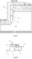
- FIG. 2a show three sectional views of an embodiment of the semi-floating-gate device disclosed in the disclosure along the length direction the device's channel.
- the semi-floating-gate device disclosed in the disclosure comprise a semiconductor substrate 200 with the first doping type and a perpendicular channel region 401 formed in the semiconductor substrate, wherein the perpendicular channel region 401 is an inversion layer formed in the semiconductor substrate 200 when the semiconductor device works.
- a source region 201 with the second doping type is formed in the bottom of the perpendicular channel region 401 and a drain region 202 with the second doping type is formed in the top of the perpendicular channel region 401.
- the semiconductor substrate 200 can be made of monocrystalline silicon, polysilicon or silicon on insulator.
- the first doping type is n type
- the second doping type is p type
- alternatively, the first doping type is p type
- the second doping type is n type.
- a first layer of insulation film 203 formed due to covering the source region, the drain region and the perpendicular channel region.
- the first layer of insulation film 203 may be made of silicon dioxide, silicon nitride, silicon oxynitride, or insulation materials with high dielectric constant, and the physical thickness preferably ranges from 1nm to 20nm.
- a floating gate 205 with the first doping type used as a charge storage node is above the first layer of insulation film 203 formed due to covering the channel region 401 and the floating gate opening region 204.
- the floating gate 205 has the doping type opposite to that of the drain region 202.
- the doped impurities in the floating gate 205 can be diffused into the drain region 202 through the floating gate opening region 204 to further form a diffusion region 402 with the first doping type, thus a p-n junction diode is formed between the floating gate 205 and the drain region 202 through the floating gate opening region 204.
- a second layer of insulation film 206 is formed due to covering the floating gate 205 and the p-n junction diode structure, wherein the second layer of insulation film 206 may be made of silicon dioxide, silicon nitride, silicon oxynitride or insulation materials with high dielectric constant, and the physical thickness preferably ranges from 1nm to 20nm.
- a control gate 207 which lies above the second layer of insulation film 206 is formed due to covering the floating gate 205 and the p-n junction diode, wherein the control gate 207 can be made of metal, alloy or doped polysilicon.
- Number 208 is a side wall of the gate of the device made of silicon dioxide or silicon nitride.
- the side wall 208 is a well-known structure in this field for isolating the control gate 207 from other conducting layers of the device.
- a doping region 210 is formed in the drain region 202, wherein the doping type of the doping region 210 is same to that of the drain region 202.
- the doping regions 210 have a doping concentration greatly higher than that of the source region 202 so as to reduce the ohmic contact of device.
- the semi-floating-gate device disclosed in the disclosure further comprises the contactor of the source region 211, the contactor of the control gate 212, the contactor of the drain region 213 and the contactor of the semiconductor substrate 214 made of conducting materials are used to connect the source region 201, the control gate 207, the drain region 202 and the semiconductor substrate 200 with the external electrode.
- FIG. 2b shows an equivalent circuit diagram of the semi-floating-gate device.
- the semi-floating-gate device disclosed in the disclosure comprises a MOSFET 36 and a gated diode 35 with the control gate 31 of MOSFET 36 as the gate, wherein the MOSFET 36 has source electrode 32, drain electrode 30, floating gate 33 and control gate 31.
- the floating gate 33 of MOSFET 36 can be connected with the anode or cathode of the gated diode 35.
- the floating gate 33 is connected with the anode of the gated diode 35.
- the floating gate 33 is charged or discharged by the gated diode 35 to change the number of the charges in the floating gate 33.
- the number of the charges determines the logic state of the semi-floating-gate device, and that means it has current or not in the perpendicular channel region.
- the semi-floating-gate device disclosed in the disclosure can be manufactured via many methods.
- the description below is the flow chart for manufacturing an embodiment of the semi-floating-gate device with n-type channel shown in FIG. 2a .
- a source region (not shown) in the semiconductor substrate 200 with the first doping type through the shallow trench isolation (STI) process.
- This STI process is well known in this field.
- the semiconductor substrate 200 can be made of monocrystalline silicon, polysilicon or silicon on insulator.
- the first doping type is p type
- the second doping type is n type.
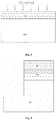
- the hard mark layer 301 on the surface of the semiconductor substrate, wherein the hard mark layer 301 can be made of silicon nitride. Then deposit a layer of optical resist 302 on the hard mark layer 301, and expose and develop it to define the position of the perpendicular channel region for device, and etch out the exposure hard make layer 301, and etch out the exposure semiconductor substrate 200 by using the hard mask layer as mask to form the perpendicular channel region in the semiconductor substrate 200.
- the etching depth is greater than the depth of the lightly-doped region 300 with the second doping type. After etching, one part of the lightly-doped region 300 with the second doping type will be left to form a drain region 202 for the device, shown as FIG.4 .
- the first layer of insulation film 203 can be made of silicon dioxide, silicon nitride, silicon oxynitride or insulation materials with high dielectric constant, and the physical thickness preferably ranges from 1nm to 20nm.
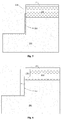
- deposit a layer of optical resist on the insulation film 203 and define the location of the floating gate opening region via the photolithographic process, and etch out the first layer of insulation film 203 exposed to form the floating gate opening region 204.
- FIG. 5 shows the condition after the optical resist is removed.
- FIG. 6 shows the condition after the optical resist is removed.
- the second layer of insulation film 206 can be made of silicon oxide, silicon nitride, silicon oxynitride or insulation materials with high dielectric constant, and the physical thickness preferably ranges from 1nm to 20nm.
- FIG. 7 shows the condition after the optical resist is removed.
- FIG. 8 shows the condition after the optical resist is removed.
- the side wall of gate 208 can be made of silicon oxide or silicon nitride.
- the semi-floating-gate device disclosed in the invention using the floating gate to store information and realizing charging or discharging of the floating gate through gated p-n junction diode boasts small unit area, high chip density and low operating voltage in data storage and strong ability in data retain.
Landscapes
- Semiconductor Memories (AREA)
- Non-Volatile Memory (AREA)
- Chemical & Material Sciences (AREA)
- Chemical Kinetics & Catalysis (AREA)
- General Chemical & Material Sciences (AREA)
- Engineering & Computer Science (AREA)
- Manufacturing & Machinery (AREA)
Abstract
Description
- The disclosure belonging to the technological field of semiconductor memory relates to a semi-floating-gate device and its manufacturing method, and more especially, to a semi-floating-gate device with perpendicular channel region and its manufacturing method.
- Semiconductor memory is widely applied in various electronic products. The requirements for construction, performance, and density of semiconductor memories in different fields are diversified. For instance, static random access memory (SRAM) has high random access rate and low integration density, while dynamic random access memory (DRAM) has high density and medium random access speed.
-
FIG. 1 shows a planar channeling semiconductor device, comprising: asource region 501 and adrain region 502 with the opposite doping type formed in the semiconductor substrate which can be made of monocrystalline silicon, polysilicon or silicon on insulator. In thesemiconductor substrate 500, a channel region 601 of the device is formed between thesource region 501 and thedrain region 502, wherein the channel region 601 is an inversion layer formed in thesemiconductor substrate 500 when the semiconductor device works. Thedoping region 509 with a high doping concentration is formed insource region 501, and the doping region 510 with a high doping concentration is formed indrain region 502, wherein the doping type of thedoping region 509 and the doping region 510 is same to that of thesource region 501 anddrain region 502. - A first layer of
insulation film 503 is formed above thesource region 501, the channel region 601 and thedrain region 502, and a floating gateopening region 504 is formed in the first layer ofinsulation film 503 on thedrain region 502. Afloating gate 505 used as a charge storage node is formed above the first layer ofinsulation film 503 and covers the channel region 601 and the floatinggate opening region 504. Thefloating gate 505 has the doping type opposite to that of thedrain region 502. The doped impurities in thefloating gate 505 can be diffused into thedrain region 502 through the floating gateopening region 504. Adiffusion region 602 is formed due to the spreading of the impurities diffusion of the floating gate 505.Thus a p-n junction diode is formed between thefloating gate 505 and thedrain region 502 through the floating gateopening region 504 blew thefloating gate 505. - A second layer of
insulation film 506 is formed due to covering thefloating gate 505 and the p-n junction diode structure. Acontrol gate 507 above the second layer ofinsulation film 506 is formed due to covering and surrounding thefloating gate 505 of the gate of thedevice 508 are formed on both side of thecontrol gate 507. The semiconductor device further comprises the contactor of thesource region 511, the contactor of thecontrol gate 507, the contactor of thedrain region 513 and the contactor of thesemiconductor substrate 514 made of conducting materials, that are used to connect thesource region 501, thecontrol gate 507, thedrain region 502 and thesemiconductor substrate 500 with the external electrode. - To guarantee the function of the semiconductor device, the planar channeling semiconductor device needs longer channel length. But the unit area of semiconductor device will be bigger, and the chip density will be reduced. It will hinder the further development of chips towards miniature direction.
- The disclosure aims at providing a semi-floating-gate device with perpendicular channel region so as to reduce the unit area of semiconductor memory and raise the density of chip.
- The disclosure provides a semi-floating-gate device with perpendicular channel region. The floating gate is half-floating, because the floating gate connects the drain region with p-n junction diode. The semi-floating-gate device specifically comprising:
- a semiconductor substrate with the first doping type;
- a perpendicular channel region formed in the semiconductor substrate;
- the bottom of the perpendicular channel region is connected with a source region with the second doping type, and the top of the perpendicular channel region is connected with a drain region with the second doping type;
- a first layer of insulation film formed due to covering the source region, the drain region and the perpendicular channel region;
- a floating gate opening region formed in the first layer of insulation film which covers the perpendicular channel region and lies above the semiconductor substrate;
- a floating gate with the first doping type which covers the first layer of the insulation film and the floating gate opening region as the charge storage node and lies above the perpendicular channel region and the floating gate opening region, and a p-n junction diode formed between floating gate and the drain region through the floating gate opening region; the floating gate can control the conducting current of the perpendicular channel region by controlling conducting field, because the floating gate covered on the first layer of the insulation film of the perpendicular channel region;
- a second layer of insulation film formed due to covering the source region, the floating gate and the p-n junction diode;
- a control gate which lies above the second layer of insulation film formed due to covering the floating gate and the p-n junction diode.
- In the semi-floating-gate device described above, the first doping type is n type, the second doping type is p type; alternatively, the first doping type is p type, and the second doping type is n type.
- In the semi-floating-gate device described above, the first layer and the second layer of insulation film are made of silicon dioxide, silicon nitride, silicon oxynitride or insulation materials with high dielectric constant, and the floating gate is made of doped polysilicon, and the control gate is made of metal, alloy, or doped polysilicon.
- In the semi-floating-gate device described above, the p-n junction diode, the second insulation film, and the control gate form a gated diode with the control gate as the gate, wherein the anode of the gated diode are connected with the floating gate region, and the cathode is connected with the drain region; alternatively, the cathode of the gated diode is connected with the floating gate region, and the anode is connected with the drain region.
- Furthermore, the disclosure also puts forward a method for manufacturing the semi-floating-gate device above, comprising:
- form a lightly-doped region with the second doping type in the semiconductor substrate with the first doping type;
- deposit a hard mark layer on the surface of the semiconductor substrate, and, define the location of a perpendicular channel region via photolithographic process and etching process;
- etch out the semiconductor substrate exposed by using the hard mask layer as mask to form the perpendicular channel region for the device, and the etching depth is greater than the depth of the lightly-doped region with the second doping type, here , after etching, one part of the lightly-doped region with the second doping type will be left to form a drain region for the device;
- etch out the left hard mask layer;
- form a first layer of insulation film on the surface of the semiconductor substrate exposed, then form a floating gate opening region via etching the first layer of insulation film ,wherein the floating gate opening region is on the top of the perpendicular channel region and expose the drain region;
- then, deposit and form a first layer of conducting film with p-type doping type on the exposure surface of the structure formed, and form a floating gate via etching the first layer of conducting film, wherein the floating gate at least cover the formed perpendicular channel region and the floating gate opening region;
- then, form a second layer of insulation film on the exposure surface of the formed structure;
- deposit and form a second layer of conducting film on the second layer of insulation film , then form a control gate for the device via photolithography and etching the second layer of conducting film;
- perform ion injection of the second doping type, and conduct doping to the control gate and the semiconductor substrate not covered by the control gate to form the a structure doped with source region, drain region and control gird.
- In the method described above, the first doping type is n type, the second doping type is p type; alternatively, the first doping type is p type, and the second doping type is n type.
- In the method described above, the first layer and the second layer of insulation film are made of silicon dioxide, silicon nitride, silicon oxynitride or insulation materials with high dielectric constant, the first layer of conducting film is made of doped polysilicon , the second layer of conducting film is made of metal, alloy, or doped polysilicon;
- The semi-floating-gate device disclosed in the disclosure using the floating gate to store information and realizing charging or discharging of the floating gate through gated p-n junction diode boasts small unit area, high chip density and low operating voltage in data storage and strong ability in data retain.
-
-
Fig. 1 is a sectional view of existing semiconductor memory; -
Fig. 2 is a sectional view of an embodiment of the semi-floating-gate device and an equivalent circuit diagram according to the disclosure; -
Figs. 3 to 10 are flow charts of an embodiment of the method for manufacturing the semi-floating-gate device according to the disclosure. - The disclosure is further detailed in combination with the drawings and the embodiments. In the figures, to facilitate illustration, the thickness of the layer and region is magnified, so the size does not represent the actual dimension. The reference figures are the schematic views of a typical embodiment for the disclosure. The embodiment shall not be limited to the specific sizes in the regions shown in the figures, but include all the shapes obtained, for example, a size with a deviation caused in manufacturing. For instance, the curve obtained through etching is generally bent or round. However, in the embodiment of the disclosure, it is indicated by a rectangle, which shall not be regarded as a limit to the scope of the disclosure.
-
FIG. 2a show three sectional views of an embodiment of the semi-floating-gate device disclosed in the disclosure along the length direction the device's channel. As shown inFIG. 2a , the semi-floating-gate device disclosed in the disclosure comprise asemiconductor substrate 200 with the first doping type and aperpendicular channel region 401 formed in the semiconductor substrate, wherein theperpendicular channel region 401 is an inversion layer formed in thesemiconductor substrate 200 when the semiconductor device works. Asource region 201 with the second doping type is formed in the bottom of theperpendicular channel region 401 and adrain region 202 with the second doping type is formed in the top of theperpendicular channel region 401. Thesemiconductor substrate 200 can be made of monocrystalline silicon, polysilicon or silicon on insulator. The first doping type is n type, the second doping type is p type, alternatively, the first doping type is p type, and the second doping type is n type. - A first layer of
insulation film 203 formed due to covering the source region, the drain region and the perpendicular channel region. A floatinggate opening region 204 formed due to covering the first layer ofinsulation film 203 of thedrain region 202 in the top of theperpendicular channel region 401. The first layer ofinsulation film 203 may be made of silicon dioxide, silicon nitride, silicon oxynitride, or insulation materials with high dielectric constant, and the physical thickness preferably ranges from 1nm to 20nm. - A floating
gate 205 with the first doping type used as a charge storage node is above the first layer ofinsulation film 203 formed due to covering thechannel region 401 and the floatinggate opening region 204. The floatinggate 205 has the doping type opposite to that of thedrain region 202. The doped impurities in the floatinggate 205 can be diffused into thedrain region 202 through the floatinggate opening region 204 to further form adiffusion region 402 with the first doping type, thus a p-n junction diode is formed between the floatinggate 205 and thedrain region 202 through the floatinggate opening region 204. - A second layer of
insulation film 206 is formed due to covering the floatinggate 205 and the p-n junction diode structure, wherein the second layer ofinsulation film 206 may be made of silicon dioxide, silicon nitride, silicon oxynitride or insulation materials with high dielectric constant, and the physical thickness preferably ranges from 1nm to 20nm. - A
control gate 207 which lies above the second layer ofinsulation film 206 is formed due to covering the floatinggate 205 and the p-n junction diode, wherein thecontrol gate 207 can be made of metal, alloy or doped polysilicon. -
Number 208 is a side wall of the gate of the device made of silicon dioxide or silicon nitride. Theside wall 208 is a well-known structure in this field for isolating thecontrol gate 207 from other conducting layers of the device. - A
doping region 210 is formed in thedrain region 202, wherein the doping type of thedoping region 210 is same to that of the drain region 202.Thedoping regions 210 have a doping concentration greatly higher than that of thesource region 202 so as to reduce the ohmic contact of device. - The semi-floating-gate device disclosed in the disclosure further comprises the contactor of the
source region 211, the contactor of thecontrol gate 212, the contactor of thedrain region 213 and the contactor of thesemiconductor substrate 214 made of conducting materials are used to connect thesource region 201, thecontrol gate 207, thedrain region 202 and thesemiconductor substrate 200 with the external electrode. - In order to further detail the structure and function of the semi-floating-gate device disclosed in the disclosure,
FIG. 2b shows an equivalent circuit diagram of the semi-floating-gate device. As shown inFIG. 2b , the semi-floating-gate device disclosed in the disclosure comprises aMOSFET 36 and agated diode 35 with thecontrol gate 31 ofMOSFET 36 as the gate, wherein theMOSFET 36 hassource electrode 32,drain electrode 30, floatinggate 33 and control gate 31.The floatinggate 33 ofMOSFET 36 can be connected with the anode or cathode of thegated diode 35. In the embodiment of the disclosure shown in the -
FIG. 2b , the floatinggate 33 is connected with the anode of thegated diode 35. The floatinggate 33 is charged or discharged by thegated diode 35 to change the number of the charges in the floatinggate 33. The number of the charges determines the logic state of the semi-floating-gate device, and that means it has current or not in the perpendicular channel region. - The semi-floating-gate device disclosed in the disclosure can be manufactured via many methods. The description below is the flow chart for manufacturing an embodiment of the semi-floating-gate device with n-type channel shown in
FIG. 2a . - Firstly, as shown in
FIG. 3 , form a source region (not shown) in thesemiconductor substrate 200 with the first doping type through the shallow trench isolation (STI) process. This STI process is well known in this field. Conduct ion injection of the second doping type into thesemiconductor substrate 200 to form a lightly-doped region 300. Thesemiconductor substrate 200 can be made of monocrystalline silicon, polysilicon or silicon on insulator. The first doping type is p type, and the second doping type is n type. - Afterwards, deposit a
hard mark layer 301 on the surface of the semiconductor substrate, wherein thehard mark layer 301 can be made of silicon nitride. Then deposit a layer of optical resist 302 on thehard mark layer 301, and expose and develop it to define the position of the perpendicular channel region for device, and etch out the exposurehard make layer 301, and etch out theexposure semiconductor substrate 200 by using the hard mask layer as mask to form the perpendicular channel region in thesemiconductor substrate 200. The etching depth is greater than the depth of the lightly-doped region 300 with the second doping type. After etching, one part of the lightly-doped region 300 with the second doping type will be left to form adrain region 202 for the device, shown asFIG.4 . - Afterwards, remove the optical resist 303 and continue to etch out the left
hard mask layer 301, and then form a first layer ofinsulation film 203 on the surface of theexposure semiconductor substrate 200, wherein the first layer ofinsulation film 203 can be made of silicon dioxide, silicon nitride, silicon oxynitride or insulation materials with high dielectric constant, and the physical thickness preferably ranges from 1nm to 20nm. Then, deposit a layer of optical resist on theinsulation film 203, and define the location of the floating gate opening region via the photolithographic process, and etch out the first layer ofinsulation film 203 exposed to form the floatinggate opening region 204.FIG. 5 shows the condition after the optical resist is removed. - Next, deposit and form a first layer of conducting film on the exposure surface of the structure formed, wherein the conducting film is made of polysilicon with p-type doping type. Then, form a floating
gate 205 via etching the first layer of conducting film, wherein the floatinggate 205 at least covers the perpendicular channel region and the floatinggate opening region 204. The impurities doped in the floatinggate 205 may be diffused into thedrain region 202 through the floatinggate opening region 204 below the floatinggate 205 to form p-type diffusion region 402, and a p-n junction diode is formed between the floatingregion 205 and thedrain region 202 through the floatinggate opening region 204.FIG. 6 shows the condition after the optical resist is removed. - Next, continue to etch out the first layer of
insulation film 203 exposed and deposit and form a second layer ofinsulation film 206 on the exposure surface of the structure formed, wherein the second layer ofinsulation film 206 can be made of silicon oxide, silicon nitride, silicon oxynitride or insulation materials with high dielectric constant, and the physical thickness preferably ranges from 1nm to 20nm. Deposit and form a second layer of conductingfilm 207 on the second layer ofinsulation film 206, wherein the second layer of conductingfilm 207 can be made of metal, alloy or doped polysilicon. Then, deposit a layer of optical resist on the second layer of conductingfilm 207, and define the location of the control gate via the photolithographic process, then etch out the second layer of conducting film exposed and form thecontrol gate 207 of the device with the remaining second layer of conductingfilm 207, wherein thecontrol gate 207 should cover the floating gate and the p-n junction diode formed.FIG. 7 shows the condition after the optical resist is removed. - Next, deposit and form a third layer of conducting film on the exposure surface of the structure formed, then deposit a layer of optical resist on the third layer of conducting film formed, and form a graph via the photolithographic process, and etch out the third layer of conducting film exposed, and continue to etch out the second layer of
insulation film 206 exposed and form the side wall ofgate 208 on the both sides of thecontrol gate 207 with the remaining third layer of conducting film. This process is well known in this field.FIG. 8 shows the condition after the optical resist is removed. The side wall ofgate 208 can be made of silicon oxide or silicon nitride. - Then, perform impurity ion injection of the second doping type (n type), and conduct doping to the
control gate 207 and thesemiconductor substrate 200 not covered by thecontrol gate 207 to form a self-aligned structure doped withsource region 201,andform doping regions 210 with high concentration in thedrain region 202, as shown inFIG. 9 . - Finally, form the contactor of the
source region 211, the contactor of thecontrol gate 212, the contactor of thedrain region 213 and the contactor of thesemiconductor substrate 214 made of conducting materials and used to connect thesource region 201, thecontrol gate 207, thedrain region 202 and the semiconductor substrate 200with the external electrode, as shown inFIG. 10 . - As described above, many embodiments with great difference may be formed under the premise that the spirit and scope of the disclosure are not deviated. It shall be understood that, the disclosure is not limited by the specific embodiment in the Specification, but restricted to the claims only.
- The semi-floating-gate device disclosed in the invention using the floating gate to store information and realizing charging or discharging of the floating gate through gated p-n junction diode boasts small unit area, high chip density and low operating voltage in data storage and strong ability in data retain.
Claims (8)
- A semi-floating-gate device, characterized in that said device comprises:a semiconductor substrate with the first doping type;a perpendicular channel region formed in the semiconductor substrate;the bottom of the perpendicular channel region is connected with a source region with the second doping type, and the top of the perpendicular channel region is connected with a drain region with the second doping type;a first layer of insulation film formed due to covering the source region, the drain region and the perpendicular channel region;a floating gate opening region formed in the first layer of insulation film which covers the perpendicular channel region and lies above the semiconductor substrate;a floating gate with the first doping type which covers the first layer of the insulation film and the floating gate opening region, and the floating gate is used as the charge storage node; and through the floating gate opening region a p-n junction diode formed between floating gate and the drain region; and the floating gate covers the first layer of the insulation film of the perpendicular channel region, controlling the current of the perpendicular channel region by controlling the electric field;a second layer of insulation film formed due to covering the source region, the floating gate and the p-n junction diode;a control gate which lies above the second layer of insulation film formed due to covering the floating gate and the p-n junction diode.
- The semi-floating-gate device as claimed in claim 1, characterized in that the first doping type is n type, the second doping type is p type; alternatively, the first doping type is p type, and the second doping type is n type.
- The semi-floating-gate device as claimed in claim 1, characterized in that the first layer and the second layer of insulation film are made of silicon dioxide, silicon nitride, silicon oxynitride or insulation materials with high dielectric constant, and the floating gate is made of doped polysilicon, and the control gate is made of metal, alloy, or doped polysilicon.
- The semi-floating-gate device as claimed in claim 1, characterized in that the p-n junction diode, the second insulation film, and the control gate form a gated diode with the control gate as the gate, wherein the anode of the gated diode are connected with the floating gate region, and the cathode is connected with the drain region; alternatively, the cathode of the gated diode is connected with the floating gate region, and the anode is connected with the drain region.
- A method for manufacturing the semi-floating-gate device as claimed in claim 1, characterized in that, comprising steps as follow:form a lightly-doped region with the second doping type in the semiconductor substrate with the first doping type;deposit a hard mark layer on the surface of the semiconductor substrate, and, define the location of a perpendicular channel region via photolithographic process and etching process;etch out the exposure semiconductor substrate by using the hard mask layer as mask to form the perpendicular channel region for the device, and the etching depth is greater than the depth of the lightly-doped region with the second doping type; here, after etching, one part of the lightly-doped region with the second doping type will be left to form a drain region for the device;etch out the left hard mask layer;form a first layer of insulation film on the surface of the semiconductor substrate exposed, then form a floating gate opening region via etching the first layer of insulation film ,wherein the floating gate opening region is on the top of the perpendicular channel region and expose the drain region;then, deposit and form a first layer of conducting film with p-type doping type on the exposure surface of the structure formed, and form a floating gate via etching the first layer of conducting film ,wherein the floating gate at least cover the formed perpendicular channel region and the floating gate opening region;then, form a second layer of insulation film on the exposure surface of the formed structure;deposit and form a second layer of conducting film on the second layer of insulation film, then form a control gate for the device via photolithography and etching the second layer of conducting film;perform ion injection of the second doping type, and conduct doping to the control gate and the semiconductor substrate not covered by the control gate to form the a structure doped with source region, drain region and control gird.
- The method for manufacturing the semi-floating-gate device as claimed in claim 5, characterized in that it further comprises:the contactor of the source region, the contactor of the control gate, the contactor of the drain region and the contactor of the semiconductor substrate that made of conducting materials are used to connect the source region, the control gate, the drain region and the semiconductor substrate with the external electrode.
- The method for manufacturing the semi-floating-gate device as claimed in claim 5, characterized in that the first doping type is n type, the second doping type is p type; alternatively, the first doping type is p type, and the second doping type is n type.
- The method for manufacturing the semi-floating-gate device as claimed in claim 5, characterized in that the first layer and the second layer of insulation film are made of silicon dioxide, silicon nitride, silicon oxynitride or insulation materials with high dielectric constant, the first layer of conducting film is made of doped polysilicon, the second layer of conducting film is made of metal, alloy, or doped polysilicon.
Applications Claiming Priority (2)
| Application Number | Priority Date | Filing Date | Title |
|---|---|---|---|
| CN2013101589714A CN103247626A (en) | 2013-05-02 | 2013-05-02 | Semi-floating gate device and manufacturing method thereof |
| PCT/CN2014/076438 WO2014177045A1 (en) | 2013-05-02 | 2014-04-29 | Semi-floating gate device and manufacturing method therefor |
Publications (2)
| Publication Number | Publication Date |
|---|---|
| EP2993695A1 true EP2993695A1 (en) | 2016-03-09 |
| EP2993695A4 EP2993695A4 (en) | 2016-12-14 |
Family
ID=48927017
Family Applications (1)
| Application Number | Title | Priority Date | Filing Date |
|---|---|---|---|
| EP14791834.6A Withdrawn EP2993695A4 (en) | 2013-05-02 | 2014-04-29 | SEMI-FLOATING GRID DEVICE AND METHOD FOR MANUFACTURING THE SAME |
Country Status (4)
| Country | Link |
|---|---|
| US (2) | US9508811B2 (en) |
| EP (1) | EP2993695A4 (en) |
| CN (1) | CN103247626A (en) |
| WO (1) | WO2014177045A1 (en) |
Cited By (1)
| Publication number | Priority date | Publication date | Assignee | Title |
|---|---|---|---|---|
| CN109036487A (en) * | 2018-07-20 | 2018-12-18 | 福州大学 | A kind of multistage optical memory and preparation method thereof based on short channel organic transistor |
Families Citing this family (34)
| Publication number | Priority date | Publication date | Assignee | Title |
|---|---|---|---|---|
| CN103247626A (en) | 2013-05-02 | 2013-08-14 | 复旦大学 | Semi-floating gate device and manufacturing method thereof |
| CN104425522B (en) * | 2013-09-10 | 2017-10-20 | 中芯国际集成电路制造(上海)有限公司 | A kind of semiconductor devices and its manufacture method |
| CN104576646B (en) * | 2013-10-11 | 2017-09-05 | 苏州东微半导体有限公司 | A kind of IC chip and its manufacture method |
| CN104637945B (en) * | 2013-11-08 | 2018-08-03 | 苏州东微半导体有限公司 | Half floating-gate memory and its manufacturing method and half floating gate memory array |
| CN103606351B (en) * | 2013-11-29 | 2016-04-20 | 中国科学院上海高等研究院 | Active matrix organic light-emitting diode pixel-driving circuit and driving method thereof |
| CN103594059B (en) * | 2013-11-29 | 2017-01-11 | 中国科学院上海高等研究院 | AMOLED (Active Matrix/Organic Light-Emitting Diode) pixel driving circuit and method |
| CN103681767B (en) * | 2013-12-19 | 2017-01-04 | 中国科学院上海高等研究院 | AMOLED pixel-driving circuit, driving method and array drive system |
| CN103680408B (en) * | 2013-12-19 | 2016-07-06 | 中国科学院上海高等研究院 | AMOLED pixel-driving circuit, driving method and array drive system |
| CN103702043B (en) * | 2014-01-03 | 2017-02-08 | 中国科学院上海高等研究院 | Fixed pattern noise (FPN) canceller circuit |
| CN103887313B (en) * | 2014-03-04 | 2016-08-31 | 华为技术有限公司 | A kind of half floating-gate device and preparation method thereof |
| CN104916639B (en) * | 2014-03-13 | 2018-09-25 | 中芯国际集成电路制造(上海)有限公司 | Half floating-gate memory structure of one kind and preparation method thereof |
| CN104916640B (en) * | 2014-03-13 | 2018-07-20 | 中芯国际集成电路制造(上海)有限公司 | A kind of half floating-gate memory structure |
| CN103972238A (en) * | 2014-03-31 | 2014-08-06 | 上海新储集成电路有限公司 | Memory unit structure |
| CN103888692B (en) * | 2014-04-01 | 2017-03-22 | 中国科学院上海高等研究院 | Image sensing device and operation method thereof |
| CN104183594B (en) * | 2014-08-17 | 2017-01-25 | 复旦大学 | Gallium nitride power device with semi-floating-gate structure |
| CN104599969A (en) * | 2015-02-02 | 2015-05-06 | 上海集成电路研发中心有限公司 | Method for reducing electric leakage of trench gate structure semi-floating gate device |
| CN104701316B (en) * | 2015-03-31 | 2017-09-29 | 上海集成电路研发中心有限公司 | Half floating-gate device and its manufacture method of a kind of pair of bathtub construction |
| US9799776B2 (en) | 2015-06-15 | 2017-10-24 | Stmicroelectronics, Inc. | Semi-floating gate FET |
| KR101958769B1 (en) * | 2017-11-16 | 2019-03-15 | 가천대학교 산학협력단 | Synaptic semiconductor device and neural networks using the same |
| CN110010605B (en) * | 2018-01-04 | 2021-04-02 | 中芯国际集成电路制造(上海)有限公司 | Memory and method of operation and formation thereof |
| CN109742073A (en) * | 2018-12-17 | 2019-05-10 | 复旦大学 | A kind of semi-floating gate transistor with high charge retention ability and preparation method thereof |
| CN109742159A (en) * | 2018-12-17 | 2019-05-10 | 复旦大学 | A kind of low tunnel leakage semi-floating gate transistor and preparation method thereof |
| CN110416287B (en) * | 2019-07-10 | 2020-10-30 | 复旦大学 | Semi-floating gate transistor of epitaxial TFET channel and preparation method thereof |
| CN112864221B (en) * | 2019-11-27 | 2022-04-15 | 苏州东微半导体股份有限公司 | Semiconductor Superjunction Power Devices |
| CN112864222B (en) * | 2019-11-27 | 2022-04-12 | 苏州东微半导体股份有限公司 | Semiconductor power device |
| US11990538B2 (en) * | 2019-11-27 | 2024-05-21 | Suzhou Oriental Semiconductor Co., Ltd. | IGBT device |
| CN112908851B (en) * | 2019-12-03 | 2022-04-15 | 苏州东微半导体股份有限公司 | Method for manufacturing semiconductor power device |
| CN111477628B (en) * | 2020-04-27 | 2022-06-21 | 复旦大学 | A kind of semi-floating gate TFT memory and preparation method thereof |
| CN114171390B (en) * | 2021-12-06 | 2026-02-10 | 复旦大学 | A semi-floating gate transistor with adjustable tunneling efficiency and its fabrication method |
| KR102932451B1 (en) * | 2022-04-27 | 2026-02-27 | 삼성전자주식회사 | Semiconductor memory device |
| CN117238340B (en) * | 2022-06-08 | 2026-01-02 | 华为技术有限公司 | In-memory computing memory, logic operation methods and electronic devices |
| CN115332360A (en) * | 2022-09-16 | 2022-11-11 | 北京大学 | PN junction injection type floating gate transistor and preparation method thereof |
| CN115692505B (en) * | 2022-11-21 | 2024-12-06 | 武汉新芯集成电路股份有限公司 | Semiconductor device and method of manufacturing and operating the same |
| CN117222226A (en) * | 2023-08-07 | 2023-12-12 | 武汉新芯集成电路制造有限公司 | Manufacturing method of storage device and storage device |
Family Cites Families (22)
| Publication number | Priority date | Publication date | Assignee | Title |
|---|---|---|---|---|
| JP3425853B2 (en) * | 1997-08-29 | 2003-07-14 | Necエレクトロニクス株式会社 | Nonvolatile semiconductor memory device |
| US6248633B1 (en) * | 1999-10-25 | 2001-06-19 | Halo Lsi Design & Device Technology, Inc. | Process for making and programming and operating a dual-bit multi-level ballistic MONOS memory |
| US6936887B2 (en) * | 2001-05-18 | 2005-08-30 | Sandisk Corporation | Non-volatile memory cells utilizing substrate trenches |
| US6996009B2 (en) * | 2002-06-21 | 2006-02-07 | Micron Technology, Inc. | NOR flash memory cell with high storage density |
| US6894339B2 (en) | 2003-01-02 | 2005-05-17 | Actrans System Inc. | Flash memory with trench select gate and fabrication process |
| US6951782B2 (en) * | 2003-07-30 | 2005-10-04 | Promos Technologies, Inc. | Nonvolatile memory cell with multiple floating gates formed after the select gate and having upward protrusions |
| US7148538B2 (en) * | 2003-12-17 | 2006-12-12 | Micron Technology, Inc. | Vertical NAND flash memory array |
| US7241654B2 (en) * | 2003-12-17 | 2007-07-10 | Micron Technology, Inc. | Vertical NROM NAND flash memory array |
| US7190616B2 (en) * | 2004-07-19 | 2007-03-13 | Micron Technology, Inc. | In-service reconfigurable DRAM and flash memory device |
| US8288813B2 (en) * | 2004-08-13 | 2012-10-16 | Infineon Technologies Ag | Integrated memory device having columns having multiple bit lines |
| US7158410B2 (en) * | 2004-08-27 | 2007-01-02 | Micron Technology, Inc. | Integrated DRAM-NVRAM multi-level memory |
| US7547599B2 (en) * | 2005-05-26 | 2009-06-16 | Micron Technology, Inc. | Multi-state memory cell |
| US7378707B2 (en) * | 2005-05-26 | 2008-05-27 | Micron Technology, Inc. | Scalable high density non-volatile memory cells in a contactless memory array |
| CN101494222B (en) * | 2008-01-23 | 2010-08-25 | 苏州东微半导体有限公司 | Semiconductor memory device, semiconductor memory array and writing method |
| US8138541B2 (en) * | 2009-07-02 | 2012-03-20 | Micron Technology, Inc. | Memory cells |
| CN101707202B (en) * | 2009-11-20 | 2012-01-11 | 苏州东微半导体有限公司 | Semiconductor photosensitization device, production method and application thereof |
| CN102169882B (en) * | 2010-02-26 | 2015-02-25 | 苏州东微半导体有限公司 | Semiconductor memory device and manufacturing method thereof |
| CN101819975B (en) * | 2010-04-28 | 2011-12-07 | 复旦大学 | Vertical channel dual-grate tunneling transistor and preparation method thereof |
| CN101901813B (en) * | 2010-07-20 | 2012-08-01 | 复旦大学 | Semiconductor memory with vertical structure and manufacturing method thereof |
| CN102456745B (en) | 2010-10-22 | 2013-09-04 | 北京大学 | Flash memory as well as preparation method and operation method thereof |
| CN102479823B (en) * | 2010-11-30 | 2014-04-16 | 中国科学院微电子研究所 | Vertical NROM storage structure and preparation method thereof |
| CN103247626A (en) | 2013-05-02 | 2013-08-14 | 复旦大学 | Semi-floating gate device and manufacturing method thereof |
-
2013
- 2013-05-02 CN CN2013101589714A patent/CN103247626A/en active Pending
-
2014
- 2014-04-29 EP EP14791834.6A patent/EP2993695A4/en not_active Withdrawn
- 2014-04-29 WO PCT/CN2014/076438 patent/WO2014177045A1/en not_active Ceased
- 2014-04-29 US US14/651,997 patent/US9508811B2/en not_active Expired - Fee Related
-
2016
- 2016-11-03 US US15/342,328 patent/US9748406B2/en not_active Expired - Fee Related
Cited By (1)
| Publication number | Priority date | Publication date | Assignee | Title |
|---|---|---|---|---|
| CN109036487A (en) * | 2018-07-20 | 2018-12-18 | 福州大学 | A kind of multistage optical memory and preparation method thereof based on short channel organic transistor |
Also Published As
| Publication number | Publication date |
|---|---|
| CN103247626A (en) | 2013-08-14 |
| EP2993695A4 (en) | 2016-12-14 |
| US9508811B2 (en) | 2016-11-29 |
| US20170148909A1 (en) | 2017-05-25 |
| WO2014177045A1 (en) | 2014-11-06 |
| US9748406B2 (en) | 2017-08-29 |
| US20150325663A1 (en) | 2015-11-12 |
Similar Documents
| Publication | Publication Date | Title |
|---|---|---|
| US9748406B2 (en) | Semi-floating-gate device and its manufacturing method | |
| US4116720A (en) | Method of making a V-MOS field effect transistor for a dynamic memory cell having improved capacitance | |
| US6440793B1 (en) | Vertical MOSFET | |
| US9741727B2 (en) | Semiconductor memory with U-shaped channel | |
| US20120112270A1 (en) | Vertical transistor having buried junction and method for manufacturing the same | |
| CN104637945B (en) | Half floating-gate memory and its manufacturing method and half floating gate memory array | |
| CN104103678A (en) | U-shaped trench type semiconductor device and manufacture method thereof | |
| US9099554B2 (en) | Semiconductor device with low on resistance and method for fabricating the same | |
| CN108305876A (en) | Semiconductor device and method for fabricating the same | |
| US10593781B2 (en) | Semiconductor device and fabrication method thereof | |
| US6414347B1 (en) | Vertical MOSFET | |
| CN103915439A (en) | Semiconductor device and manufacturing method thereof | |
| US9666484B2 (en) | Integrated circuit protected from short circuits caused by silicide | |
| US9147835B2 (en) | Tunnel transistor structure integrated with a resistance random access memory (RRAM) and a manufacturing method thereof | |
| US4225879A (en) | V-MOS Field effect transistor for a dynamic memory cell having improved capacitance | |
| KR100517219B1 (en) | Dram cell arrangement with dynamic gain memory cells, and method for the production thereof | |
| CN113380870B (en) | Semiconductor device manufacturing method | |
| US11652170B2 (en) | Trench field effect transistor structure free from contact hole | |
| US11658239B2 (en) | Semiconductor device and fabrication method thereof | |
| US20250142878A1 (en) | Semiconductor device and manufacturing method thereof | |
| US12439605B2 (en) | Semiconductor device, three-dimensional memory and method for fabricating the semiconductor device | |
| US12342575B2 (en) | Semiconductor structure and method making the same | |
| US8138541B2 (en) | Memory cells | |
| CN210296297U (en) | Memory and Semiconductor Devices | |
| CN114335147A (en) | Terminal structure, manufacturing method thereof and semiconductor device |
Legal Events
| Date | Code | Title | Description |
|---|---|---|---|
| PUAI | Public reference made under article 153(3) epc to a published international application that has entered the european phase |
Free format text: ORIGINAL CODE: 0009012 |
|
| 17P | Request for examination filed |
Effective date: 20150528 |
|
| AK | Designated contracting states |
Kind code of ref document: A1 Designated state(s): AL AT BE BG CH CY CZ DE DK EE ES FI FR GB GR HR HU IE IS IT LI LT LU LV MC MK MT NL NO PL PT RO RS SE SI SK SM TR |
|
| AX | Request for extension of the european patent |
Extension state: BA ME |
|
| RIN1 | Information on inventor provided before grant (corrected) |
Inventor name: SUN, QINGQING Inventor name: WANG, PENGFEI Inventor name: ZHANG, WEI |
|
| DAX | Request for extension of the european patent (deleted) | ||
| A4 | Supplementary search report drawn up and despatched |
Effective date: 20161114 |
|
| RIC1 | Information provided on ipc code assigned before grant |
Ipc: H01L 27/115 20060101ALI20161108BHEP Ipc: H01L 29/788 20060101AFI20161108BHEP Ipc: H01L 21/28 20060101ALI20161108BHEP Ipc: H01L 29/423 20060101ALI20161108BHEP Ipc: H01L 29/66 20060101ALI20161108BHEP Ipc: H01L 21/8239 20060101ALI20161108BHEP |
|
| STAA | Information on the status of an ep patent application or granted ep patent |
Free format text: STATUS: THE APPLICATION HAS BEEN WITHDRAWN |
|
| 18W | Application withdrawn |
Effective date: 20170427 |