EP2975788A2 - Optische übertragungsvorrichtung und detektionsvorrichtung - Google Patents
Optische übertragungsvorrichtung und detektionsvorrichtung Download PDFInfo
- Publication number
- EP2975788A2 EP2975788A2 EP15176429.7A EP15176429A EP2975788A2 EP 2975788 A2 EP2975788 A2 EP 2975788A2 EP 15176429 A EP15176429 A EP 15176429A EP 2975788 A2 EP2975788 A2 EP 2975788A2
- Authority
- EP
- European Patent Office
- Prior art keywords
- band
- optical
- change
- spectrum
- signal
- Prior art date
- Legal status (The legal status is an assumption and is not a legal conclusion. Google has not performed a legal analysis and makes no representation as to the accuracy of the status listed.)
- Granted
Links
Images


Classifications
-
- H—ELECTRICITY
- H04—ELECTRIC COMMUNICATION TECHNIQUE
- H04B—TRANSMISSION
- H04B10/00—Transmission systems employing electromagnetic waves other than radio-waves, e.g. infrared, visible or ultraviolet light, or employing corpuscular radiation, e.g. quantum communication
- H04B10/07—Arrangements for monitoring or testing transmission systems; Arrangements for fault measurement of transmission systems
- H04B10/075—Arrangements for monitoring or testing transmission systems; Arrangements for fault measurement of transmission systems using an in-service signal
- H04B10/079—Arrangements for monitoring or testing transmission systems; Arrangements for fault measurement of transmission systems using an in-service signal using measurements of the data signal
- H04B10/0795—Performance monitoring; Measurement of transmission parameters
- H04B10/07955—Monitoring or measuring power
-
- H—ELECTRICITY
- H04—ELECTRIC COMMUNICATION TECHNIQUE
- H04B—TRANSMISSION
- H04B10/00—Transmission systems employing electromagnetic waves other than radio-waves, e.g. infrared, visible or ultraviolet light, or employing corpuscular radiation, e.g. quantum communication
- H04B10/50—Transmitters
- H04B10/501—Structural aspects
- H04B10/503—Laser transmitters
- H04B10/505—Laser transmitters using external modulation
- H04B10/5057—Laser transmitters using external modulation using a feedback signal generated by analysing the optical output
-
- H—ELECTRICITY
- H04—ELECTRIC COMMUNICATION TECHNIQUE
- H04B—TRANSMISSION
- H04B10/00—Transmission systems employing electromagnetic waves other than radio-waves, e.g. infrared, visible or ultraviolet light, or employing corpuscular radiation, e.g. quantum communication
- H04B10/50—Transmitters
- H04B10/564—Power control
-
- H—ELECTRICITY
- H04—ELECTRIC COMMUNICATION TECHNIQUE
- H04B—TRANSMISSION
- H04B10/00—Transmission systems employing electromagnetic waves other than radio-waves, e.g. infrared, visible or ultraviolet light, or employing corpuscular radiation, e.g. quantum communication
- H04B10/50—Transmitters
- H04B10/58—Compensation for non-linear transmitter output
Definitions
- An embodiment discussed herein relates to an optical transmission apparatus and a detection apparatus.
- JP 2007-208472 A and JP 2008-92172 A disclose techniques related to an optical communication system and an optical transmitter.
- an optical modulator and a driver e.g. an electrical amplifier
- a drive signal having an amplitude corresponding to a double (2 x Vn) half-wavelength voltage Vn is applied to an optical modulator for an optical QPSK (Quadrature Phase Shift Keying) scheme.
- QPSK Quadrature Phase Shift Keying
- a digital signal processing is applied to an optical transmitter in the optical communication system.
- signals with various formats such as a dispersion pre-equalization signal, a Nyquist signal and a quadrature amplitude modulation (QAM) signal are generated by using the digital signal processing.
- QAM quadrature amplitude modulation
- the dispersion pre-equalization signal it is possible to compensate for wavelength dispersion which occurs in transmission light propagating in an optical transmission line to expand a transmission distance of the transmission light.
- a Nyquist signal which is subjected to a band limitation with a Nyquist filter in the digital signal processing, it is possible to improve frequency usage efficiency according to the band limitation.
- a QAM signal it is possible to transmit a greater amount of information than that of, for example, a phase-shift keying (PSK) signal to expand transmission capacity.
- PSK phase-shift keying
- the optical modulator may be driven by a drive signal with an amplitude smaller than 2 x Vn.
- the optical modulator and the driver may be operated in a linear region.
- an object of the present invention is to prevent a deterioration in quality of signal light due to a change in characteristics of a drive signal applied to an optical modulator.
- an optical transmission apparatus may include an optical modulator, a detector, and a controller.
- the optical modulator is driven by a drive signal which is generated from an electrical signal.
- the electrical signal is obtained by performing a digital signal processing on a data signal.
- the detector is configured to detect a change in a spectrum of output light of the optical modulator.
- the controller is configured to control the digital signal processing based on a detection result of the detector.
- an optical transmission apparatus may include an optical modulator, a detector, and a controller.
- the optical modulator is driven by a drive signal which is generated from an electrical signal.
- the electrical signal is obtained by performing a digital signal processing on a data signal.
- the detector is configured to detect a change in a spectrum of output light of the optical modulator.
- the controller is configured to notify an external apparatus of information indicative of an occurrence of a band change in the output light of the optical modulator in response to a detection that the change in the spectrum detected by the detector exceeds a predetermined change amount.
- a detection apparatus may include a drive signal generator and a detector.
- the drive signal generator is configured to generate a drive signal for an optical modulator from an electrical signal.
- the electrical signal is obtained by performing a digital signal processing on a data signal.
- the detector is configured to detect a change in a difference between optical power of a first band and optical power of a second band.
- the first band corresponds to a partial band of the spectrum including a center frequency of the spectrum of the output light of the optical modulator.
- the second band corresponds to a partial band of the spectrum different from the first band.
- FIG. 1 is a block diagram illustrating an exemplary configuration of an optical transmitter (may be also referred to as an "optical transmission apparatus") according to one embodiment.
- the optical transmitter 1 illustrated in FIG. 1 includes, for example, an electrical signal generator 11, drivers 12I and 12Q, a light source 13, an optical modulator 14 which includes an optical modulator 141, an optical coupler 15, a monitor 16, and a controller 17.
- a reference numeral "2" denotes a system control apparatus 2 that controls an entire optical transmission system including the optical transmitter 1.
- a non-restrictive example of the system control apparatus 2 may be an NMS (Network Management System) or the like.
- the electrical signal generator 11 performs a digital signal processing on a transmission data signal, and generates an electrical signal (e.g. voltage signal) which is a drive signal for the optical modulator 14.
- the electrical signal generator (may also be referred to as a "drive signal generator") 11 illustratively includes a digital signal processor (DSP) 111, and digital-analog converters (DAC) 112I and 112Q.
- DSP digital signal processor
- DAC digital-analog converters
- the DSP 111 is an example of a processor having arithmetic operation capability.
- the DSP 111 performs a digital signal processing on a transmission data signal according to a modulation format to generate a transmission digital signal.
- An example of the modulation format is a Nyquist QPSK (Quadrature Phase Shift Keying).
- Modulated signal light obtained by the Nyquist QPSK may correspond to signal light obtained by performing a band limitation with a Nyquist filter of a digital signal processing on a transmission data signal.
- the Nyquist QPSK is an example of a modulation format which drives the optical modulator 141 with a drive signal having an amplitude smaller than an amplitude corresponding to double (2 x Vn) half-wavelength voltage Vn.
- Driving the optical modulator 141 with the drive signal having the amplitude smaller than 2 x Vn may be considered as corresponding to operating the optical modulator 141 in a non-saturated region (e.g. linear region) rather than in a saturated region.
- Modulation formats of operating the optical modulator 141 in the linear region are not limited to the Nyquist QPSK.
- Examples of the other modulation formats may include M-level quadrature amplitude modulation format such as 2 M -QAM (Quadrature Amplitude Modulation).
- M is an integer equal to or more than 2 and represents a multi-level. As the multi-level is larger, it is possible to transmit a greater amount of information per single modulation.
- a differential modulation format or a polarization-multiplexing scheme may be combined with the QPSK or the QAM to further increase the available amount of transmission information per single modulation.
- the differential modulation format is an example of a modulation format of allocating different information bits to a plurality of differential signals shifted in phases.
- the QPSK and the QAM using the differential signals may be referred to as a DPSK (Differential PSK) and a DQAM (Differential QAM), respectively.
- the polarization-multiplexing scheme is an example of allocating different information bits to different polarizations (e.g. an X-polarization and a Y-polarization) of light to multiplex the information bits.
- the QPSK and the QAM using the polarization-multiplexing scheme may be referred to as a DP (Dual Polarization)-QPSK and a DP-QAM, respectively.
- Each of the DACs 112I and 112Q in the electrical signal generator 11 convert a transmission digital signal generated by the DSP 111 into an analog signal.
- One of the DACs 112I and 112Q (for example, DAC 112I) converts a signal corresponding to in-phase components (or I components), when a transmission digital signal is allocated (or mapped) to symbols represented by a complex plane (or IQ plane), into an analog signal.
- the other DAC 112Q converts a signal corresponding to quadrature phase components (or Q components), when the transmission digital signal is mapped to symbols represented by the IQ plane, into an analog signal.
- Both of the drivers 12I and 12Q may be, for example, electrical amplifiers and provided for the individual components and the Q components.
- the drivers 12I and 12Q amplify the analog electrical signals input from the corresponding DACs 112I and 112Q such that the analog signals have appropriate amplitudes for drive signals applied to the optical modulator 141.
- one driver 12I generates a drive signal having the amplitude corresponding to the analog electrical signal of the I components input from the DAC 112I to apply the generated drive signal to a drive electrode provided for an optical waveguide which forms an I-arm of the optical modulator 141.
- the other driver 12Q generates a drive signal having the amplitude corresponding to the analog electrical signal of the Q components input from the DAC 112Q and corresponding to apply the generated drive signal to a drive electrode provided for an optical waveguide which forms a Q-arm of the optical modulator 141.
- the light source 13 may be, for example, a semiconductor laser diode (LD) which emits light with a wavelength.
- the light source 13 may be a tunable LD which is variable in light emission wavelength. Output light of the light source 13 is input to the optical modulator 141.
- LD semiconductor laser diode
- the optical modulator 141 may be illustratively an LN modulator with a lithium niobate (LiNbO3), and may include the optical waveguide which forms the I-arm and the optical waveguide which forms the Q-arm. Further, the optical modulator 141 may include an optical branch which branches light from the light source 13 to the I-arm and the Q-arm, and an optical interferer at which light propagating through the I-arm and the Q-arm joins and interferes.
- LiNbO3 lithium niobate
- the I-arm and the Q-arm are respectively provided with the drive electrodes as described above, and the drive signals are applied to the drive electrodes from the corresponding drivers 12I and 12Q.
- the refractive index of the I-arm and Q-arm are changed in response to changes in the applied drive signals.
- the phases of light propagating through the I-arm and Q-arm are changed in response to the change of refractive index.
- the intensity of light output from the optical interferer changes.
- the optical modulator 141 modulates transmission light input from the light source 13 by the drive signals according to the transmission data signals to generate modulated signal light.
- a photo detector (PD) 143 may be provided inside or outside the optical modulator 141.
- the PD 143 may receive any one or more of: input light input to the optical modulator 141; light propagating in one or both of the I-arm and the Q-arm; and output light of the optical modulator 141 as appropriate.
- the PD 143 generates an electrical signal corresponding to an optical power of the received light.
- the electrical signal may be used to, for example, control (e.g., feedback-control) a drive signal of the optical modulator 141.
- the optical coupler 15 branches (may also be referred to as "tap") the modulated signal light output from the optical modulator 141.
- One of branched lights is output as transmission light to an optical transmission line, and the other of the branched lights is output as monitor light to the monitor 16.
- the monitor 16 monitors (may also be referred to as "detect") characteristics of the drive signal of the optical modulator 141 based on the monitor light input from the optical coupler 15.
- the characteristics of monitoring target are, for example, frequency response of the drive signal.
- the monitor 16 may also be referred to as a "measurer 16".
- a waveform (or spectrum) of the modulated signal light output from the optical modulator 141 are also changed in response to the change in the frequency response.
- the waveform of the modulated signal light may be shifted from a waveform (may also be referred to as an "ideal waveform") which is expected as a result of the application of the digital signal processing.
- the "waveform shift" causes a deterioration in quality of the transmission signal light transmitted by the optical transmitter 1.
- the monitor 16 monitors the output light of the optical modulator 141 to enable, for example, the controller 17 to detect a change in the frequency response of the drive signal.
- the detailed method of detecting the change in the frequency response will be described later.
- the monitor 16 and the controller 17 may be considered as an example of a "detection apparatus” or a “detector” which detects a change in the spectrum of the output light of the optical modulator 141.
- the controller 17 monitors quality (for example, a change in a band described later) of the modulated signal light (in other words, transmission signal light) based on a monitoring result of the monitor 16. When determining that the quality goes below a predetermined quality, the controller 17 may notify information indicative of a deterioration in transmission signal quality to the system control apparatus 2 available to control the entire optical transmission system in which the optical transmitter 1 is used.
- quality for example, a change in a band described later
- the controller 17 may notify information indicative of a deterioration in transmission signal quality to the system control apparatus 2 available to control the entire optical transmission system in which the optical transmitter 1 is used.
- the system control apparatus 2 In response to a reception of the notification indicative of the deterioration in the quality, the system control apparatus 2 is available to perform control or adjustment to compensate for the deterioration in the signal quality for the entire optical transmission system. Accordingly, it is possible to improve the transmission quality of the entire optical transmission system.
- the electrical signal generator 11, the drivers 12I and 12Q, the optical modulator 14 and the monitor 16 are illustrated in separate blocks. However, these blocks may be integrated 1 or a part of the blocks may be integrated in the optical transmitter. Further, in FIG. 1 , there is one drive signal for each of the I-arm and the Q-arm. However, the drive signals may be two or more differential signals for each of the I-arm and the Q-arm.
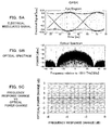
- FIG. 2 is a diagram illustrating examples of spectra of modulated signal light when an electrical signal (may also be referred to as an "electrical modulated signal") obtained by modulating a transmission data signal with the Nyquist QPSK in the electrical signal generator 11 (DSP 111) is applied as a drive signal to the optical modulator 141.
- an electrical signal may also be referred to as an "electrical modulated signal”
- DSP 111 the electrical signal generator 11
- the spectrum at the top of the three spectra illustrated in FIG. 2 is the most close to ideal spectrum (e.g. rectangular shape) of the Nyquist QPSK modulated signal light.
- the spectrum illustrated at the middle in FIG. 2 has a relatively unsharp waveform compared with the that of the spectrum at the top stage, and the spectrum illustrated at the bottom in FIG. 2 has a further unsharp waveform compared with that of the spectrum at the middle.
- FIG. 2 illustrates that the spectrum of the Nyquist QPSK deteriorates from the ideal spectrum in order from the top to the bottom. Focusing upon, for example, a portion (or a band) encircled by a dotted frame A in FIG. 2 , optical power tends to lower near an end portion of the spectrum of the modulated signal light.
- Such a change (or deterioration) in the spectrum may be referred to as "a band change (or band deterioration)".
- the band change may be caused by a change in characteristics of the drive signals given to the optical modulator 141 from the electrical signal generator 11 through the drivers 12I and 12Q (in other words, electrical paths from the electrical signal generator 11 to the optical modulator 141) illustrated in FIG. 1 . Therefore, it is possible to detect the change in the characteristics of the drive signal by detecting the band change.
- a non-restrictive example detects, as illustrated in FIG. 3 , optical power (Pfc) of a first band including a center frequency (fc) of the modulated signal light and optical power (Pf ⁇ ) of a second band including a frequency (fc + f ⁇ ) shifted from the center frequency fc by f ⁇ in a positive frequency as the center frequency of the second band.
- a separation frequency f ⁇ shifted from the center frequency fc may be set to a half of a baud rate B (i.e., B/2) or substantially set to the B/2. Further, bandwidths of the first band and the second band are not limited in particular, yet may be set to the B/2 or substantially set to the B/2.
- the first band may be a partial band of the spectrum of the modulated signal light, and may have the bandwidth of B/2 whose center frequency is the center frequency fc of the modulated signal light.
- the second band may be a partial band of the spectrum of the modulated signal light different from the first band, and may have the bandwidth of B/2 whose center frequency is the frequency fc + f ⁇ shifted from the center frequency fc of the modulated signal light by f ⁇ .
- the second band corresponds to a band near the end (e.g., the right end in FIG. 3 ) of the spectrum.
- Light in the first band and the second band can be detected (or filtered) by, for example, using an optical filter.
- characteristics indicated by a solid line 100 indicate first filter characteristics which allow the light in the first band to pass (or transmit)
- characteristics indicated by a dotted line 200 indicate second filter characteristics which allow the light in the second band to pass (or transmit).
- the filter center frequency of the first filter characteristics 100 corresponds to the center frequency fc of the modulated signal light, and the filter bandwidth of the first filter characteristics 100 is B/2.
- the filter center frequency of the second filter characteristics 200 corresponds to the frequency fc + f ⁇ shifted from the center frequency fc of the modulated signal light by f ⁇ , and the filter bandwidth of the second filter characteristics 200 is B/2.
- the first filter characteristics 100 and the second filter characteristics 200 may be realized as characteristics of individual optical filters, or may be realized by changing a transmission center frequency of one optical filter with a variable filter center frequency.
- a change corresponding to the band change appears in the difference P (hereinafter, may also be referred to as an "optical power difference P") as illustrated in FIG. 4 , for example.
- the change in the optical power difference P tends to increase as the band change increases.
- the "change in the optical power difference P" may also be referred to simply as an "optical power change".
- output optical power of the optical modulator 141 may fluctuate due to a factor such as a fluctuation in the output optical power of the light source 13, which is different from the change in characteristics of a drive signal.
- a monitoring target band hereinafter, may also be referred to as a "monitor band”
- a monitor band may be set to a single band.
- Driving the optical modulator 141 with a drive signal of a normal QPSK electrical modulated signal corresponds to driving the optical modulator 141 with a drive signal having the amplitude of 2 x Vn to operate the optical modulator 141 in the saturated region.
- FIG. 5A illustrates an exemplary waveform of the normal QPSK electrical modulated signal
- FIG. 5B illustrates an exemplary spectrum of the modulated signal light when the QPSK electrical modulated signal illustrated in FIG. 5A is applied as a drive signal to the optical modulator 141.
- FIG. 5C illustrates an example of a change in the optical power difference P in response to the band change when the QPSK electrical modulated signal illustrated in FIG. 5A is applied as a drive signal to the optical modulator 141.
- the change in the optical power difference P due to the band change does not occur or is not available to be detected with sufficient sensitivity even if the change occurs.
- FIG. 6B is a diagram illustrating an exemplary spectrum of the modulated signal light when the Nyquist QPSK electrical modulated signal illustrated in FIG. 6A is applied as a drive signal to the optical modulator 141.
- FIG. 6C is a diagram corresponding to FIG. 4 .
- a modulation format which may cause a change in the optical power difference P in response to the band change is not limited to the Nyquist QPSK.
- the optical modulator 141 when a 16 QAM electrical modulated signal is applied as a drive signal to the optical modulator 141, the optical modulator 141 also operates in the linear region. Therefore, it is possible to detect the band change by detecting the optical power difference P.
- FIG. 7A illustrates an exemplary waveform of the 16 QAM electrical modulated signal
- FIG. 7B illustrates an exemplary spectrum of modulated signal light when the 16 QAM electrical modulated signal illustrated in FIG. 7A is applied as a drive signal to the optical modulator 141.
- FIG. 7C illustrates an example of a change in the optical power difference P in response to the band change when the 16 QAM electrical modulated signal illustrated in FIG. 7A is applied as the drive signal to the optical modulator 141.
- the 16 QAM electrical modulated signal illustrated in FIG. 7A is applied as the drive signal to the optical modulator 141.
- FIG. 7C even when the 16 QAM electrical modulated signal is applied as the drive signal to the optical modulator 141, it is possible to detect the band change by detecting the optical power difference P.
- FIG. 8 is a block diagram illustrating an exemplary configuration of the monitor 16 illustrated in FIG. 1 .
- the monitor 16 illustrated in FIG. 8 illustratively includes a tunable optical filter 161 and an optical power meter 162.
- the tunable optical filter 161 is illustratively an optical filter whose transmission center wavelength (frequency) is variable.
- the first and second filter characteristics 100 and 200 illustrated in FIG. 3 are realize by controlling the transmission center wavelength of the optical filter 161.
- the setting or changing of the transmission center wavelength may be controlled by the controller 17 illustrated in FIG. 1 .
- the optical power meter 162 detects (or measures) power of light passed through the tunable optical filter 161 when the tunable optical filter 161 is set to have the first and second filter characteristics 100 and 200.
- the optical power meter 162 measures the optical power Pfc of the first band including the center frequency fc of the modulated signal light, and the optical power Pf ⁇ of the second band including the center frequency of the frequency (fc + f ⁇ ) shifted from the center frequency fc by f ⁇ in the positive frequency.
- the measurement results are output to the controller 17.
- the controller 17 calculates the optical power difference P as described above based on the measurement results of the optical power meter 162. In order to detect the change in the optical power difference P, the controller 17 may store the measurement results of the optical power meter 162 at different measurement timings into a memory 171 illustrated in FIG. 8 , for example.
- One of the different measurement timings may be a timing at which the optical transmitter 1 is activated, and another timing (corresponds to a second measurement timing) may be a timing after the optical transmitter 1 is activated (e.g. an arbitrary timing during an operation).
- the controller 17 detects the change in the optical power difference P based on the optical power difference P obtained from the measurement results at the different measurement timings and compares the detected change with a threshold value.
- the threshold value may be set to a value corresponding to a predetermined change amount (or deterioration amount) of the detected change in the relationship illustrated in FIG. 4 .
- the threshold value may be set to the change amount of the optical power difference P corresponding to "-3 GHz" of the band change (or band deterioration).
- the threshold value may be stored in the memory 171.
- the controller 17 may notify the system control apparatus 2 such as the NMS of an occurrence of deterioration in quality of the modulated signal light transmitted by the optical transmitter 1.
- the notification may be performed by, for example, a communication unit 172 illustrated in FIG. 8 .
- the monitor 16 illustrated in FIG. 8 measures the optical power Pfc and the optical power Pf ⁇ of the different monitor bands by controlling the transmission center frequency of the single tunable optical filter 161 with the optical power meter 162.
- individual optical filters may be provided for the individual monitor bands.
- a measurement function of the monitor 16 may be achieved by using an optical spectrum analyzer 163 as illustrated in FIG. 9 .
- the optical spectrum analyzer 163 would be costly, the exemplary configuration illustrated in FIG. 8 is advantageous in that the monitor 16 can be achieved by a simple configuration and at low cost.
- the monitor 16 measures the optical power Pfc of the first band including the center frequency fc of modulated signal light, and the optical power Pf ⁇ of the second band shifted from the center frequency fc by substantially +B/2.
- the measurement results are output to the controller 17.
- the measurement results at the activation of the system may be considered as initial measurement results.
- the controller 17 stores the received measurement results in, for example, the memory 171 (processing P11).
- the controller 17 obtains measurement results of the optical power Pfc and Pf ⁇ from the monitor 16 again, and detects a change in the optical power difference P based on the measurement results and the initial measurement results stored in the memory 171 (processing P12).
- the controller 17 compares the detected change amount of the optical power difference P with the threshold value stored in the memory 171 to check whether or not the change amount of the optical power difference P exceeds the threshold value (in other words, whether or not the change amount exceeds a predetermined deterioration amount) (processing P13).
- the controller 17 In response to a detection that the change amount of the optical power difference P exceeds the predetermined deterioration amount (Yes in the processing P13), the controller 17 enables, for example, the communication unit 172 to notify the system control apparatus 2 of an occurrence of deterioration in quality of the modulated signal light transmitted by the optical transmitter 1 (processing P14).
- the controller 17 returns to the processing P12, and continues monitoring the change in the optical power difference P during operations of the system.
- the band change (or band deterioration) occurred in the modulated signal due to a change in characteristics of the drive signal applied to the optical modulator 141. Further, since the detected band change is notified to the system control apparatus 2, it is possible to perform control or adjustment to compensate for a deterioration in signal quality in the entire optical transmission system. Accordingly, it is possible to improve transmission quality of the entire optical transmission system.
- the DSP 111 may include a band compensation processing of the drive signal (or electrical signal) as an example of the digital signal processing, and may control the band compensation processing to compensate for (e.g. minimize) the band change detected by the monitor 16 based on the band change information notified from the controller 17. In other words, the controller 17 may control the digital signal processing performed by the DSP 111 to compensate for the band change detected by the monitor 16.
- the two monitor bands are set to the spectrum of modulated signal light.
- three monitor bands may be set as illustrated in FIG. 11 , for example.
- An exemplary configuration of the monitor 16 in the second example may be the same as the configuration illustrated in FIG. 8 or 9 .
- the first band corresponding to the filter characteristics 100 and the second band corresponding to the filter characteristics 200 may be the same as the bands described already with reference to FIG. 3 .
- the third band corresponding to the filter characteristics 300 may be set to a symmetrical band with respect to the second band around the first band.
- the first to third bands corresponding to the filter characteristics 100 to 300 may also be referred to as the first to third monitor bands 100 to 300, respectively, for descriptive purpose.
- the third monitor band 300 may correspond to a band including a center frequency of a frequency (fc - f ⁇ ) shifted from the center frequency fc of modulated signal light by substantially half (B/2) of a baud rate in a negative frequency. Further, the bandwidth of the third monitor band 300 may also be about B/2.
- the monitor 16 may set the filter characteristics 100 to 300 corresponding to the three monitor bands by changing one of the transmission center frequency of the tunable optical filter 161, or the filter characteristics 100 to 300 maybe realized by using individual optical filters.
- the optical power meter 162 measures optical power Pfc, P(+f ⁇ ) and P(-f ⁇ ) of the three monitor bands 100 to 300.
- Pfc is the optical power of the first monitor band 100 including the center frequency fc of the modulated signal light.
- Pf(+f ⁇ ) is the optical power of the second monitor band 200 shifted from the center frequency fc by substantially +B/2.
- P(-f ⁇ ) is the optical power of the third monitor band 300 shifted from the center frequency fc by substantially -B/2.
- the two or three different monitor bands are set to the spectrum of modulated signal light.
- two different monitor bands 100 and 400 having different bandwidths and including the same monitor band may be set as illustrated in FIG. 12 , for example.
- the first monitor band 100 may be the same as the band 100 illustrated in FIGS. 3 and 7 .
- the first monitor band 100 may have the center frequency fc and the bandwidth corresponding to substantially half of a baud rate (B/2).
- the second monitor band 400 may have the center frequency fc and the bandwidth which includes a whole band of the spectrum of modulated signal light.
- a non-restrictive example of the bandwidth of the second monitor band 400 may be a bandwidth corresponding to 1.2 times (1.2 x B) of the baud rate.
- Filter characteristics corresponding to the two monitor bands 100 and 400 may be set by changing a transmission bandwidth of a single variable band wavelength optical filter which has the transmission center frequency fc and variable transmission bandwidth.
- the filter characteristics corresponding to the two monitor band 100 and 400 may be achieved by using individual optical filters.
- FIG. 13 illustrates an exemplary configuration of the monitor 16 provided with a variable band wavelength optical filter 161a.
- the variable band wavelength optical filter 161a may have not only a variable transmission bandwidth but also a variable transmission center wavelength. One or both of the transmission bandwidth and the transmission center wavelength of the variable band wavelength optical filter 161a may be controlled (or set) by the controller 17.
- the optical power meter 162 of the monitor 16 illustrated in FIG. 13 measures optical power Pfc and Pfall of the two monitor bands 100 and 400.
- FIG. 14 illustrates an exemplary configuration of the optical transmitter 1 using the polarization-multiplexing scheme.
- the optical modulator 14 of the optical transmitter 1 illustrated in FIG. 14 may include, for example, a polarization beam splitter (PBS) 140, optical modulators 141X and 141Y respectively corresponding to different polarizations (e.g. an X-polarization and a Y-polarization), and a polarization beam combiner (PBC) 142.
- PBS polarization beam splitter
- PBC polarization beam combiner
- the PBS 140 separates transmission light input from the light source 13 to X-polarization components and Y-polarization components.
- the separated X-polarization components are input to the optical modulator 141X and the separated Y-polarization components are input to the optical modulator 141Y.
- Each of the optical modulators 141X and 141Y may have the same configuration as that of the optical transmitter 1 illustrated in FIG. 1 .
- each of the optical modulator 141X and 141Y may include an optical branch, an I-arm, a Q-arm and an optical interferer.
- the optical branch receives an input of light of the polarization components separated by the PBS 140.
- one or both of the optical modulators 141X and 141Y may be provided with a PD 143 in a manner similar to the configuration of FIG. 1 . In other words, individual power of different polarization components in modulated signal light is monitored by the PD 143.
- the I-arm and the Q-arm of the optical modulator 141X corresponding to the X-polarization components may also be referred to as an "XI-arm” and an "XQ-arm", respectively, for descriptive purpose.
- the I-arm and the Q-arm of the optical modulator 141Y corresponding to the Y-polarization components may also be referred to as a "YI-arm” and a "YQ-arm”, respectively, for descriptive purpose.
- Light of the X-polarization components separated by the PBS 140 propagates in the XI-arm and the XQ-arm.
- Light of the Y-polarization components separated by the PBS 140 propagates in the YI-arm and the YQ-arm.
- Each of the XI-arm, the XQ-arm, the YI-arm and the YQ-arm may be provided with a drive electrode which is not illustrated.
- the respective drive electrodes are supplied drive signals by drivers 12XI, 12XQ, 12YI and 12YQ, respectively.
- Each of the drivers 12XI, 12XQ, 12YI and 12YQ may be an electrical amplifier similar to the drivers 12I and 12Q illustrated in FIG. 1 .
- the drivers 12XI, 12XQ, 12YI and 12YQ receive analog electrical modulated signals generated by the electrical signal generator 11 for the different X-polarization components and the Y-polarization components, and for in-phase (I) components and quadrature (Q) components.
- the electrical signal generator 11 may include, for example, a DSP 111, and a DAC 112XI, a DAC 112XQ, a DAC 112YI and a DAC 112YQ corresponding to the different X-polarization and Y-polarization components and the in-phase (I) components and the quadrature (Q) components.
- the DSP 111 performs a digital signal processing including a digital modulation processing such as the Nyquist QPSK and the 16QAM on a transmission data signal to generate digital electrical modulated signals of the X-polarization components and the Y-polarization components, and the I components and the Q components.
- a digital modulation processing such as the Nyquist QPSK and the 16QAM
- the generated digital electrical signal modulated signals are converted into analog electrical modulated signals by the DACs 112XI, 112XQ, 112YI and 112YQ corresponding to the above-described four arms, respectively.
- the analog electrical modulated signals are supplied to the corresponding drivers 12XI, 12XQ, 12YI and 12YQ.
- Each of the drivers 12XI, 12XQ, 12YI and 12YQ amplify the input analog electrical modulated signal such that the individual analog electrical modulated signal has an appropriate amplitude as a drive signal supplied to the optical modulator 141X or the optical modulator 141Y.
- the refractive index of the corresponding arms change, and the phase of transmission light propagating in each arm changes.
- the intensity of the light output from each optical interferer of each of the optical modulators 141X and 141Y changes.
- the transmission light of the different X-polarization and Y-polarization components from the light source 13 is modulated by the optical modulators 141X and 141Y with the drive signals corresponding to transmission data signal to generate modulated signal light.
- the modulated signal light of the X-polarization components output from the one optical modulator 141X and the modulated signal light of the Y-polarization components output from the other optical modulator 141Y are input to the PBC 142.
- the PBC 142 may combines (may also be referred to "polarization-multiplexes") light of the X-polarization components and the Y-polarization components.
- the polarization-multiplexed light is output as polarization-multiplexed transmission light to an optical transmission line from the optical transmitter 1.
- Part of the polarization-multiplexed signal light is tapped to the monitor 16 by the optical coupler 15.
- the monitor 16 may have the same configuration as the configuration illustrated in FIG. 8 , 9 or 13 .
- the monitor 16 and the controller 17 illustrated in FIG. 14 is possible to detect a band change in the spectrum of the polarization-multiplexed signal light output from the optical modulator 14 by using the detection method described with reference to FIG. 3 , 11 or 12 .
- the controller 17 may notify (or feedback) band change information to the DSP 111 as indicated by a dotted line arrow in FIG. 14 similar to FIG. 1 .
- the DSP 111 may control the band compensation processing on the drive signals of the electrical signals based on the notified band change information. Further, when the controller 17 detects that the band change of the polarization-multiplexed transmission light exceeds the threshold value and deteriorated, the communication unit 172 may notify the system control apparatus 2 of an occurrence of determination in quality due to the band deterioration of the polarization-multiplexed transmission light transmitted by the optical transmitter 1.
- control signal a monitor signal or a control signal (hereinafter, may collectively be referred to as a "control signal”) is superimposed on modulated signal light (which may also be polarization-multiplexed transmission light) output from the optical modulator 14.
- control signal having a low frequency which is sufficiently lower than the frequency of the modulated signal light may be superimposed on the modulated signal light.
- the low frequency signal may be, for example, at orders of mega hertz while the frequency of modulated signal light is at orders of giga bits.
- the low frequency signal which is an example of the control signal may be generated by performing a digital signal processing on a transmission data signal by a DSP 111 of an electrical signal generator 11 as illustrated in FIG. 15 , for example.
- the low frequency signal e.g., with 1 MHz in FIG. 15
- the low frequency signal is superimposed on the drive signal applied to the optical modulator 14. Consequently, the low frequency signal subjected to an amplitude modulation is superimposed on the modulated signal light.
- the monitor 16 for example, the optical power meter 162 and the spectrum analyzer 163 or a controller 17 may average the optical power of monitor light for a longer period of time than the fluctuation cycle.
- the controller 17 may perform feedback control such that the DSP 111 changes the low frequency signal (1 MHz) to be superimposed to another frequency (for example, 10 MHz) which does not impact on monitoring of the monitor 16.
- the detection of the band change by using the monitor 16 and the controller 17 is compatible with a control using the control signal.
- the number of target monitor bands (hereinafter, may also be referred to as "monitor points" for descriptive purpose) of the monitor 16 may be fixed or variable.
- a DSP 111 of the electrical signal generator 11 changes a modulation format to be applied to a transmission data signal during operations of the system.
- the number of monitor points may also be changed.
- the change amount of optical power difference P measured by the monitor 16 may also be changed.
- monitoring sensitivity of the monitor 16 fluctuates according to the modulation format of the digital signal processing in the DSP 111.
- the controller 17 may adaptively control filter characteristic of the tunable optical filter 161 provided in the monitor according to the change in the modulation format. Accordingly, it is possible to set the number of monitor points suitable for the modulation format.
- the number of monitor points with respect to a modulation format may be set (or stored) in a memory 171 of the controller 17 in advance.
- Information available to identify the modulation format (hereinafter, may also be referred to as "modulation format information") may be given to the controller 17 from an external apparatus such as the system control apparatus 2.
- the modulation format information may be stored in the memory 171 of the controller 17.
- controller 17 including controlling the number of monitor points according to a modulation format will be described with reference to a flowchart illustrated in FIG. 17 .
- the controller 17 may perform pre-processing indicated by processing P21 when the optical transmitter 1 is activated in response to an activation of the optical transmission system, for example. For example, in pre-processing P21, the controller 17 sets filter characteristics of the tunable optical filter 161 such that light at monitor point including the center frequency fc of modulated signal light is input to an optical power meter 162.
- the optical power meter 162 detects (or measures) optical power Pfc of light passed through the tunable optical filter 161 at the monitor point including the center frequency fc.
- the controller 17 stores information of the optical power Pfc detected by the optical power meter 162 in the memory 171.
- the controller 17 sets the filter characteristics of the tunable optical filter 161 such that the light of the monitor point including a frequency shifted from the center frequency fc of the modulated signal light by substantially ⁇ B/n (n is an integer equal to or more than 1) is input to the optical power meter 162.
- the controller 17 changes the filter characteristics of the tunable optical filter 161 for a plurality of monitor points by changing the value of "n".
- the optical power meter 162 detects (or measures) the optical power P(f ⁇ n*f ⁇ ) at a corresponding monitor point per value of "n".
- the controller 17 stores information of the optical power P(f ⁇ n*f ⁇ ) detected by the optical power meter 162 in the memory 171, for example.
- optical power which serves as the reference for a monitor point may also be referred to as "reference optical power" for descriptive purpose.
- the controller 17 selects monitor points corresponding to the number of monitor points N#i (an integer satisfying ⁇ n) for the identified modulation format among from a plurality of monitor points stored in the memory 171 in pre-processing P21. Further, the controller 17 controls the filter characteristics of the tunable optical filter 161 such that light of the selected monitor points (hereinafter, may also be referred to the "selected monitor points") is input to the optical power meter 162.
- the optical power meter 162 detects (or measures) the optical power of the selected monitor points, and a detection results are given to the controller 17 (to processing P23-i from Yes route of processing P22-i).
- the controller 17 detects an optical power difference between optical power of the selected monitor points and the reference optical power of the selected monitor points stored in in the memory 171 in pre-processing P21, and checks whether or not the change in the optical power difference exceeds a threshold value (processing P24-i).
- the threshold value may be set (or stored) in the memory 171 in advance for each modulation format.
- the communication unit 172 of the controller 17 notifies the system control apparatus 2 of an occurrence of the band change (or band deterioration) in the modulated signal light, for example (processing P25).
- the controller 17 performs processing of identifying (which may also be referred to as "monitor") the modulation format depicted by processing P22-i.
- the controller 17 may finish monitoring the band change in the modulated signal light by using the monitor 16.
- the communication unit 172 of the controller 17 notifies the system control apparatus 2 of an event that the detected band change exceeds the predetermined deterioration amount. Therefore, the system control apparatus 2 is possible to perform control or adjustment to compensate for a deterioration in signal quality in the entire optical transmission system. Accordingly, it is possible to improve transmission quality in the entire optical transmission system.
- FIG. 18 is a block diagram illustrating an exemplary configuration of an optical transmission system (which may also be referred to as an "optical network").
- the optical transmission system 3 illustrated in FIG. 18 may include, for example, a plurality of ROADMs (Reconfigurable optical add-drop multiplexer) 31
- the ROADMs 31 may be optically and communicably connected by optical transmission lines 4.
- the optical transmission system 3 illustrated in FIG. 18 is a "mesh network" in which the ROADMs 31 are connected by the optical transmission lines 4 in a mesh topology.
- the optical transmission system 3 may be an optical network with other topologies such as a ring network.
- the ROADM 31 is an example of an optical transmission apparatus.
- the optical transmission apparatus may also be referred to as a "station” or a "node”.
- Each ROADM 31 may include, for example, a function of branching (or dropping) light in units of wavelength, an insertion (or add) function, and a through function.
- the drop function makes it possible to drop to a transceiver 32 light with any one of wavelengths included in wavelength-division multiplexing (WDM) light received through the optical transmission line 4.
- WDM wavelength-division multiplexing
- the light dropped to the transceiver 32 may be referred to as a "drop light”.
- the add function makes it possible to add light (which may also be referred to as "add light”) with a wavelength transmitted from the transceiver 32 to the WDM light received through the optical transmission line 4.
- the through function makes it possible to transmit (or pass through) light of any one of the wavelengths included in the WDM light received through the optical transmission line 4 to an optical channel 4 corresponding to a different degree.
- the transceiver 32 may include a receiver which receives the drop light and a transmitter which transmits the add light.
- the transceiver 32 may also be referred to as a "transponder 32".
- the receiver receives and demodulates the drop light, and remaps the resulting signal on a frame signal of a client network (which may also be referred to as a "tribute network").
- the client network may be the Ethernet (registered trademark) or a synchronous digital network such as SDH or SONET.
- the WDM light transmitted through the optical transmission line 4 may be transmitted in an OTN (Optical Transport Network) frame.
- OTN Optical Transport Network
- the receiver may convert the OTN frame of the received drop light into a frame signal of the client network such as an Ethernet frame.
- the received drop light may be received by way of coherent reception.
- the receiver may be a coherent receiver.
- the coherent receiver is available to selectively receive the light with the wavelength corresponding to a wavelength of local light.
- the wavelength of local light corresponds to "a target reception wavelength" of the transponder 32, and the target reception wavelength can be controlled by using a tunable laser diode (LD) for a local light source.
- LD tunable laser diode
- the transmitter may include a transmission light source which emits light of a wavelength (which may be referred to as an "add wavelength” or a “transmission wavelength”) corresponding to add light, an optical modulator which modulates the light of the transmission wavelength with a transmission data signal.
- a transmission light source which emits light of a wavelength (which may be referred to as an "add wavelength” or a “transmission wavelength”) corresponding to add light
- an optical modulator which modulates the light of the transmission wavelength with a transmission data signal.
- the transmission data signal may be generated by a digital signal processing circuit.
- the digital signal processing circuit may perform a digital modulation processing and a digital waveform shaping processing on a transmission data signal. By performing the digital modulation processing, it is possible to superimpose an auxiliary data signal (which may be referred to as an "auxiliary signal") on the transmission data.
- the transmission data signal which may be referred to as a main signal
- FSK Frequency Shift Keying
- the auxiliary signal may be a monitor control signal or some kind of a measurement signal.
- the auxiliary signal may also be referred to as an "auxiliary channel”.
- the digital waveform shaping processing may include a Nyquist filtering.
- a Nyquist filtering By applying the waveform shaping processing to the transmission data signal using the Nyquist filtering, it is possible to narrow the spectrum of transmission modulated signal light obtained by the optical modulator. Since the spectrum can be narrowed, it is also possible to support multicarrier transmission such as a "super channel" transmission.
- the ROADM 31 may be provided with an optical performance monitor (OPM) 33 which monitors power of WDM light received from the optical transmission line 4, WDM light transmitted to the optical transmission line 4, the drop light, the add light, and the through light, as illustrated in FIG. 18 .
- OPM optical performance monitor
- the OPM 33 may include, for example, an optical filter 331, a PD (photo detector or photo diode) 332 and a processor (which may be referred to as a "controller”) 333.
- the optical filter 331 may be an optical band pass filter, and allows light of a monitoring target band of input light to pass to the PD 332, for example.
- the optical filter 331 may be a tunable optical filter.
- the tunable optical filter is available to monitor light of an arbitrary wavelength included in the WDM light by changing a transmission wavelength.
- the PD 332 receives light passed through the optical filter 331, and outputs an electrical signal (e.g. current signal) corresponding to optical power of the received light.
- the current signal corresponding to the received optical power at the PD 332 may be converted into a voltage signal by a transimpedance amplifier (TIA), for example.
- TIA transimpedance amplifier
- the FSK signal components are superimposed as an auxiliary signal on the light input to the optical filter 331, the FSK signal components are converted into the amplitude modulated signal by filtering in the optical filter 331. Accordingly, an electrical signal having amplitude components corresponding to the amplitude modulated signal appears in the output of the PD 332, and this electrical signal is detected as the auxiliary signal.
- the processor 333 performs a monitor processing of checking whether or not signal light satisfies, for example, a power level or an OSNR (Optical to Signal Noise Ratio) based on the electrical signal corresponding to the received optical power input from the PD 332.
- the processor 333 may perform a processing (which may include a monitor control and a measurement) according to the detected auxiliary signal.
- the OPM 33 including the optical filter 331 and the PD 332 may be provided in the node 31.
- the optical filter 331 of the OPM 33 can be shared by the optical filter 161 or the optical filter 161a for the above-described monitor 16. In other words, it is possible to realize the above-described monitor 16 by using the optical filter 331 of the OPM 33 existing in the node 31.
- the optical filter 331 when the optical filter 331 is the tunable optical filter, the optical filter 331 can be used for the tunable optical filter 161 illustrated in FIG. 8 .
- the optical filter 331 when the optical filter 331 is the variable band wavelength optical filter, the optical filter 331 can be used for the variable band wavelength optical filter 161a illustrated in FIG. 13 .
- the processor 333 of the OPM 33 is possible to detect the band change of modulated signal light in a manner similar to the above-described example by performing the above-described processing of the controller 17.
- the processor 333 may be considered to correspond to the controller 17.
- the optical filter 331 provided in the OPM 33 is an optical filter with a fixed passband
- the optical filter 331 is only necessary to be replaced with the tunable optical filter 161 or the variable band wavelength optical filter 161a.
- an optical filter 334 corresponding to the tunable optical filter 161 or the variable band wavelength optical filter 161a may be added to the OPM 33 in addition to the optical filter 331.
- an optical power meter 335 may be provided in the OPM 33. The optical power meter 335 may be considered to correspond to the above-described optical power meter 162.
- the above-described monitor 16 can be achieved by using the existing OPM 33 provided in the node 31, it is possible to detect the band change of the main signal light without additional optical components for the monitor 16 or with the minimum additional optical components. Accordingly, it is possible to implement a function of the monitor 16 on the node 31 at low cost.
Landscapes
- Physics & Mathematics (AREA)
- Electromagnetism (AREA)
- Engineering & Computer Science (AREA)
- Computer Networks & Wireless Communication (AREA)
- Signal Processing (AREA)
- Optics & Photonics (AREA)
- Nonlinear Science (AREA)
- Optical Modulation, Optical Deflection, Nonlinear Optics, Optical Demodulation, Optical Logic Elements (AREA)
- Optical Communication System (AREA)
- Spectrometry And Color Measurement (AREA)
Applications Claiming Priority (1)
| Application Number | Priority Date | Filing Date | Title |
|---|---|---|---|
| JP2014146074A JP6519999B2 (ja) | 2014-07-16 | 2014-07-16 | 光送信装置及び検出装置 |
Publications (3)
| Publication Number | Publication Date |
|---|---|
| EP2975788A2 true EP2975788A2 (de) | 2016-01-20 |
| EP2975788A3 EP2975788A3 (de) | 2016-04-20 |
| EP2975788B1 EP2975788B1 (de) | 2019-09-25 |
Family
ID=53541584
Family Applications (1)
| Application Number | Title | Priority Date | Filing Date |
|---|---|---|---|
| EP15176429.7A Active EP2975788B1 (de) | 2014-07-16 | 2015-07-13 | Optische übertragungsvorrichtung und detektionsvorrichtung |
Country Status (3)
| Country | Link |
|---|---|
| US (1) | US9667344B2 (de) |
| EP (1) | EP2975788B1 (de) |
| JP (1) | JP6519999B2 (de) |
Families Citing this family (12)
| Publication number | Priority date | Publication date | Assignee | Title |
|---|---|---|---|---|
| US9749057B2 (en) | 2012-12-28 | 2017-08-29 | Juniper Networks, Inc. | Detection and alignment of XY skew |
| JP6323193B2 (ja) * | 2014-06-12 | 2018-05-16 | 富士通株式会社 | 光送信装置および故障判断方法 |
| JP2016142799A (ja) * | 2015-01-30 | 2016-08-08 | 住友大阪セメント株式会社 | 光制御素子 |
| JP6481557B2 (ja) * | 2015-08-03 | 2019-03-13 | 富士通株式会社 | 光受信装置及び信号処理方法 |
| JP6613761B2 (ja) * | 2015-09-24 | 2019-12-04 | 富士通株式会社 | 光伝送システム、波長可変光フィルタの制御装置及び制御方法 |
| CN107024744A (zh) * | 2016-01-29 | 2017-08-08 | 青岛海信宽带多媒体技术有限公司 | 一种光模块及波长监控方法 |
| US9998232B2 (en) * | 2016-09-13 | 2018-06-12 | Juniper Networks, Inc. | Detection and compensation of power imbalances for a transmitter |
| JP7024234B2 (ja) * | 2017-07-18 | 2022-02-24 | 富士通株式会社 | 光送信機、及び光送信機の制御方法 |
| WO2020196129A1 (ja) * | 2019-03-25 | 2020-10-01 | 日本電気株式会社 | 光伝送システム、光送信機および光通信方法 |
| WO2023105589A1 (ja) * | 2021-12-06 | 2023-06-15 | 日本電信電話株式会社 | 制御回路及び光回路制御方法 |
| WO2023119673A1 (ja) * | 2021-12-24 | 2023-06-29 | 学校法人明治大学 | 評価装置、光受信器、光通信システム、プログラム及び評価方法 |
| WO2024261987A1 (ja) | 2023-06-22 | 2024-12-26 | 学校法人明治大学 | 制御装置、補償装置、光受信装置、光通信システム、プログラム及び制御方法 |
Citations (2)
| Publication number | Priority date | Publication date | Assignee | Title |
|---|---|---|---|---|
| JP2007208472A (ja) | 2006-01-31 | 2007-08-16 | Fujitsu Ltd | 光送信器 |
| JP2008092172A (ja) | 2006-09-29 | 2008-04-17 | Fujitsu Ltd | 光送信機 |
Family Cites Families (10)
| Publication number | Priority date | Publication date | Assignee | Title |
|---|---|---|---|---|
| AU3162401A (en) * | 1999-12-24 | 2001-07-09 | Corning O.T.I Inc. | Method of analog modulation and optical emitter using this method |
| JP2002023119A (ja) * | 2000-06-30 | 2002-01-23 | Mitsubishi Electric Corp | 光送信装置およびこれに用いる光変調器の出力安定化制御方法 |
| US8050351B2 (en) | 2003-07-02 | 2011-11-01 | Celight, Inc. | Quadrature modulator with feedback control and optical communications system using the same |
| US7336877B2 (en) * | 2004-08-31 | 2008-02-26 | Corning Incorporated | Broadband optical fiber |
| KR100859808B1 (ko) * | 2007-01-05 | 2008-09-24 | 삼성전자주식회사 | 광 출력 모듈의 에러 감지 및 복구를 수행하는 광 네트워크유닛 및 그 제어 방법 |
| JP5476697B2 (ja) | 2008-09-26 | 2014-04-23 | 富士通株式会社 | 光信号送信装置 |
| US8649688B2 (en) * | 2011-01-28 | 2014-02-11 | Ciena Corporation | Radio frequency drive level control system and method for an electro-optic phase modulator |
| EP2634934B1 (de) | 2012-01-10 | 2016-05-04 | Alcatel Lucent | Optischer Sender |
| US8958705B2 (en) * | 2012-01-13 | 2015-02-17 | Esi-Pyrophotonics Lasers Inc. | Methods and systems for a pulsed laser source emitting a predetermined output pulse profile |
| JP6031963B2 (ja) * | 2012-11-21 | 2016-11-24 | 富士通株式会社 | 光送信装置、光送信方法、および光送信プログラム |
-
2014
- 2014-07-16 JP JP2014146074A patent/JP6519999B2/ja active Active
-
2015
- 2015-07-09 US US14/794,873 patent/US9667344B2/en active Active
- 2015-07-13 EP EP15176429.7A patent/EP2975788B1/de active Active
Patent Citations (2)
| Publication number | Priority date | Publication date | Assignee | Title |
|---|---|---|---|---|
| JP2007208472A (ja) | 2006-01-31 | 2007-08-16 | Fujitsu Ltd | 光送信器 |
| JP2008092172A (ja) | 2006-09-29 | 2008-04-17 | Fujitsu Ltd | 光送信機 |
Also Published As
| Publication number | Publication date |
|---|---|
| EP2975788A3 (de) | 2016-04-20 |
| JP6519999B2 (ja) | 2019-05-29 |
| JP2016025380A (ja) | 2016-02-08 |
| US20160020853A1 (en) | 2016-01-21 |
| EP2975788B1 (de) | 2019-09-25 |
| US9667344B2 (en) | 2017-05-30 |
Similar Documents
| Publication | Publication Date | Title |
|---|---|---|
| EP2975788B1 (de) | Optische übertragungsvorrichtung und detektionsvorrichtung | |
| US9831947B2 (en) | Margin determination systems and methods in optical networks | |
| US8655170B2 (en) | OSNR monitor device and OSNR measurement device | |
| JP6589276B2 (ja) | 光伝送装置、光伝送システム、及び、送信波長制御方法 | |
| US9071378B2 (en) | Superimposed signal detection circuit and optical node equipment | |
| US9503211B2 (en) | Signal detection circuit and optical transmission equipment | |
| US10951344B2 (en) | Optical transmitter, optical receiver, and optical transmission system | |
| JP6613761B2 (ja) | 光伝送システム、波長可変光フィルタの制御装置及び制御方法 | |
| JP5712935B2 (ja) | 波長分散を検出する方法及び装置並びに波長分散を補償する方法及び装置 | |
| JP2010081287A (ja) | 光信号送信装置 | |
| US9515727B2 (en) | In-band optical signal-to-noise ratio monitor | |
| US20120128351A1 (en) | Communication system, measuring apparatus, transmitting apparatus, and measurement method | |
| US9515733B2 (en) | Mitigation of spectral offset in an optical filter | |
| JP6349696B2 (ja) | 光送信装置、光受信装置および光通信方法 | |
| US10374703B2 (en) | Transmission device and signal monitoring method | |
| US10069567B2 (en) | Optical communication system, optical receiver and optical transmitter | |
| EP2983311A1 (de) | Vorrichtung zur optischen übertragung, system zur optischen übertragung und steuerungsverfahren für ein system zur optischen übertragung | |
| JP6323193B2 (ja) | 光送信装置および故障判断方法 | |
| US20160337039A1 (en) | Optical transmitting device and optical receiving device |
Legal Events
| Date | Code | Title | Description |
|---|---|---|---|
| PUAI | Public reference made under article 153(3) epc to a published international application that has entered the european phase |
Free format text: ORIGINAL CODE: 0009012 |
|
| AK | Designated contracting states |
Kind code of ref document: A2 Designated state(s): AL AT BE BG CH CY CZ DE DK EE ES FI FR GB GR HR HU IE IS IT LI LT LU LV MC MK MT NL NO PL PT RO RS SE SI SK SM TR |
|
| AX | Request for extension of the european patent |
Extension state: BA ME |
|
| PUAL | Search report despatched |
Free format text: ORIGINAL CODE: 0009013 |
|
| AK | Designated contracting states |
Kind code of ref document: A3 Designated state(s): AL AT BE BG CH CY CZ DE DK EE ES FI FR GB GR HR HU IE IS IT LI LT LU LV MC MK MT NL NO PL PT RO RS SE SI SK SM TR |
|
| AX | Request for extension of the european patent |
Extension state: BA ME |
|
| RIC1 | Information provided on ipc code assigned before grant |
Ipc: H04B 10/58 20130101ALI20160314BHEP Ipc: H04B 10/50 20130101AFI20160314BHEP |
|
| 17P | Request for examination filed |
Effective date: 20161019 |
|
| RBV | Designated contracting states (corrected) |
Designated state(s): AL AT BE BG CH CY CZ DE DK EE ES FI FR GB GR HR HU IE IS IT LI LT LU LV MC MK MT NL NO PL PT RO RS SE SI SK SM TR |
|
| STAA | Information on the status of an ep patent application or granted ep patent |
Free format text: STATUS: REQUEST FOR EXAMINATION WAS MADE |
|
| R17P | Request for examination filed (corrected) |
Effective date: 20161019 |
|
| STAA | Information on the status of an ep patent application or granted ep patent |
Free format text: STATUS: EXAMINATION IS IN PROGRESS |
|
| 17Q | First examination report despatched |
Effective date: 20180716 |
|
| GRAP | Despatch of communication of intention to grant a patent |
Free format text: ORIGINAL CODE: EPIDOSNIGR1 |
|
| STAA | Information on the status of an ep patent application or granted ep patent |
Free format text: STATUS: GRANT OF PATENT IS INTENDED |
|
| INTG | Intention to grant announced |
Effective date: 20190508 |
|
| GRAS | Grant fee paid |
Free format text: ORIGINAL CODE: EPIDOSNIGR3 |
|
| GRAA | (expected) grant |
Free format text: ORIGINAL CODE: 0009210 |
|
| STAA | Information on the status of an ep patent application or granted ep patent |
Free format text: STATUS: THE PATENT HAS BEEN GRANTED |
|
| AK | Designated contracting states |
Kind code of ref document: B1 Designated state(s): AL AT BE BG CH CY CZ DE DK EE ES FI FR GB GR HR HU IE IS IT LI LT LU LV MC MK MT NL NO PL PT RO RS SE SI SK SM TR |
|
| REG | Reference to a national code |
Ref country code: GB Ref legal event code: FG4D |
|
| REG | Reference to a national code |
Ref country code: CH Ref legal event code: EP |
|
| REG | Reference to a national code |
Ref country code: AT Ref legal event code: REF Ref document number: 1184838 Country of ref document: AT Kind code of ref document: T Effective date: 20191015 |
|
| REG | Reference to a national code |
Ref country code: IE Ref legal event code: FG4D |
|
| REG | Reference to a national code |
Ref country code: DE Ref legal event code: R096 Ref document number: 602015038559 Country of ref document: DE |
|
| REG | Reference to a national code |
Ref country code: NL Ref legal event code: MP Effective date: 20190925 |
|
| PG25 | Lapsed in a contracting state [announced via postgrant information from national office to epo] |
Ref country code: BG Free format text: LAPSE BECAUSE OF FAILURE TO SUBMIT A TRANSLATION OF THE DESCRIPTION OR TO PAY THE FEE WITHIN THE PRESCRIBED TIME-LIMIT Effective date: 20191225 Ref country code: SE Free format text: LAPSE BECAUSE OF FAILURE TO SUBMIT A TRANSLATION OF THE DESCRIPTION OR TO PAY THE FEE WITHIN THE PRESCRIBED TIME-LIMIT Effective date: 20190925 Ref country code: HR Free format text: LAPSE BECAUSE OF FAILURE TO SUBMIT A TRANSLATION OF THE DESCRIPTION OR TO PAY THE FEE WITHIN THE PRESCRIBED TIME-LIMIT Effective date: 20190925 Ref country code: LT Free format text: LAPSE BECAUSE OF FAILURE TO SUBMIT A TRANSLATION OF THE DESCRIPTION OR TO PAY THE FEE WITHIN THE PRESCRIBED TIME-LIMIT Effective date: 20190925 Ref country code: FI Free format text: LAPSE BECAUSE OF FAILURE TO SUBMIT A TRANSLATION OF THE DESCRIPTION OR TO PAY THE FEE WITHIN THE PRESCRIBED TIME-LIMIT Effective date: 20190925 Ref country code: NO Free format text: LAPSE BECAUSE OF FAILURE TO SUBMIT A TRANSLATION OF THE DESCRIPTION OR TO PAY THE FEE WITHIN THE PRESCRIBED TIME-LIMIT Effective date: 20191225 |
|
| REG | Reference to a national code |
Ref country code: LT Ref legal event code: MG4D |
|
| PG25 | Lapsed in a contracting state [announced via postgrant information from national office to epo] |
Ref country code: LV Free format text: LAPSE BECAUSE OF FAILURE TO SUBMIT A TRANSLATION OF THE DESCRIPTION OR TO PAY THE FEE WITHIN THE PRESCRIBED TIME-LIMIT Effective date: 20190925 Ref country code: GR Free format text: LAPSE BECAUSE OF FAILURE TO SUBMIT A TRANSLATION OF THE DESCRIPTION OR TO PAY THE FEE WITHIN THE PRESCRIBED TIME-LIMIT Effective date: 20191226 Ref country code: RS Free format text: LAPSE BECAUSE OF FAILURE TO SUBMIT A TRANSLATION OF THE DESCRIPTION OR TO PAY THE FEE WITHIN THE PRESCRIBED TIME-LIMIT Effective date: 20190925 |
|
| REG | Reference to a national code |
Ref country code: AT Ref legal event code: MK05 Ref document number: 1184838 Country of ref document: AT Kind code of ref document: T Effective date: 20190925 |
|
| PG25 | Lapsed in a contracting state [announced via postgrant information from national office to epo] |
Ref country code: PT Free format text: LAPSE BECAUSE OF FAILURE TO SUBMIT A TRANSLATION OF THE DESCRIPTION OR TO PAY THE FEE WITHIN THE PRESCRIBED TIME-LIMIT Effective date: 20200127 Ref country code: ES Free format text: LAPSE BECAUSE OF FAILURE TO SUBMIT A TRANSLATION OF THE DESCRIPTION OR TO PAY THE FEE WITHIN THE PRESCRIBED TIME-LIMIT Effective date: 20190925 Ref country code: RO Free format text: LAPSE BECAUSE OF FAILURE TO SUBMIT A TRANSLATION OF THE DESCRIPTION OR TO PAY THE FEE WITHIN THE PRESCRIBED TIME-LIMIT Effective date: 20190925 Ref country code: IT Free format text: LAPSE BECAUSE OF FAILURE TO SUBMIT A TRANSLATION OF THE DESCRIPTION OR TO PAY THE FEE WITHIN THE PRESCRIBED TIME-LIMIT Effective date: 20190925 Ref country code: AT Free format text: LAPSE BECAUSE OF FAILURE TO SUBMIT A TRANSLATION OF THE DESCRIPTION OR TO PAY THE FEE WITHIN THE PRESCRIBED TIME-LIMIT Effective date: 20190925 Ref country code: EE Free format text: LAPSE BECAUSE OF FAILURE TO SUBMIT A TRANSLATION OF THE DESCRIPTION OR TO PAY THE FEE WITHIN THE PRESCRIBED TIME-LIMIT Effective date: 20190925 Ref country code: NL Free format text: LAPSE BECAUSE OF FAILURE TO SUBMIT A TRANSLATION OF THE DESCRIPTION OR TO PAY THE FEE WITHIN THE PRESCRIBED TIME-LIMIT Effective date: 20190925 Ref country code: PL Free format text: LAPSE BECAUSE OF FAILURE TO SUBMIT A TRANSLATION OF THE DESCRIPTION OR TO PAY THE FEE WITHIN THE PRESCRIBED TIME-LIMIT Effective date: 20190925 Ref country code: AL Free format text: LAPSE BECAUSE OF FAILURE TO SUBMIT A TRANSLATION OF THE DESCRIPTION OR TO PAY THE FEE WITHIN THE PRESCRIBED TIME-LIMIT Effective date: 20190925 |
|
| PG25 | Lapsed in a contracting state [announced via postgrant information from national office to epo] |
Ref country code: IS Free format text: LAPSE BECAUSE OF FAILURE TO SUBMIT A TRANSLATION OF THE DESCRIPTION OR TO PAY THE FEE WITHIN THE PRESCRIBED TIME-LIMIT Effective date: 20200224 Ref country code: SK Free format text: LAPSE BECAUSE OF FAILURE TO SUBMIT A TRANSLATION OF THE DESCRIPTION OR TO PAY THE FEE WITHIN THE PRESCRIBED TIME-LIMIT Effective date: 20190925 Ref country code: SM Free format text: LAPSE BECAUSE OF FAILURE TO SUBMIT A TRANSLATION OF THE DESCRIPTION OR TO PAY THE FEE WITHIN THE PRESCRIBED TIME-LIMIT Effective date: 20190925 Ref country code: CZ Free format text: LAPSE BECAUSE OF FAILURE TO SUBMIT A TRANSLATION OF THE DESCRIPTION OR TO PAY THE FEE WITHIN THE PRESCRIBED TIME-LIMIT Effective date: 20190925 |
|
| REG | Reference to a national code |
Ref country code: DE Ref legal event code: R097 Ref document number: 602015038559 Country of ref document: DE |
|
| PG2D | Information on lapse in contracting state deleted |
Ref country code: IS |
|
| PG25 | Lapsed in a contracting state [announced via postgrant information from national office to epo] |
Ref country code: DK Free format text: LAPSE BECAUSE OF FAILURE TO SUBMIT A TRANSLATION OF THE DESCRIPTION OR TO PAY THE FEE WITHIN THE PRESCRIBED TIME-LIMIT Effective date: 20190925 Ref country code: IS Free format text: LAPSE BECAUSE OF FAILURE TO SUBMIT A TRANSLATION OF THE DESCRIPTION OR TO PAY THE FEE WITHIN THE PRESCRIBED TIME-LIMIT Effective date: 20200126 |
|
| PLBE | No opposition filed within time limit |
Free format text: ORIGINAL CODE: 0009261 |
|
| STAA | Information on the status of an ep patent application or granted ep patent |
Free format text: STATUS: NO OPPOSITION FILED WITHIN TIME LIMIT |
|
| 26N | No opposition filed |
Effective date: 20200626 |
|
| PG25 | Lapsed in a contracting state [announced via postgrant information from national office to epo] |
Ref country code: SI Free format text: LAPSE BECAUSE OF FAILURE TO SUBMIT A TRANSLATION OF THE DESCRIPTION OR TO PAY THE FEE WITHIN THE PRESCRIBED TIME-LIMIT Effective date: 20190925 |
|
| PG25 | Lapsed in a contracting state [announced via postgrant information from national office to epo] |
Ref country code: MC Free format text: LAPSE BECAUSE OF FAILURE TO SUBMIT A TRANSLATION OF THE DESCRIPTION OR TO PAY THE FEE WITHIN THE PRESCRIBED TIME-LIMIT Effective date: 20190925 |
|
| REG | Reference to a national code |
Ref country code: CH Ref legal event code: PL |
|
| REG | Reference to a national code |
Ref country code: BE Ref legal event code: MM Effective date: 20200731 |
|
| PG25 | Lapsed in a contracting state [announced via postgrant information from national office to epo] |
Ref country code: LI Free format text: LAPSE BECAUSE OF NON-PAYMENT OF DUE FEES Effective date: 20200731 Ref country code: LU Free format text: LAPSE BECAUSE OF NON-PAYMENT OF DUE FEES Effective date: 20200713 Ref country code: CH Free format text: LAPSE BECAUSE OF NON-PAYMENT OF DUE FEES Effective date: 20200731 |
|
| PG25 | Lapsed in a contracting state [announced via postgrant information from national office to epo] |
Ref country code: BE Free format text: LAPSE BECAUSE OF NON-PAYMENT OF DUE FEES Effective date: 20200731 |
|
| PG25 | Lapsed in a contracting state [announced via postgrant information from national office to epo] |
Ref country code: IE Free format text: LAPSE BECAUSE OF NON-PAYMENT OF DUE FEES Effective date: 20200713 |
|
| PG25 | Lapsed in a contracting state [announced via postgrant information from national office to epo] |
Ref country code: TR Free format text: LAPSE BECAUSE OF FAILURE TO SUBMIT A TRANSLATION OF THE DESCRIPTION OR TO PAY THE FEE WITHIN THE PRESCRIBED TIME-LIMIT Effective date: 20190925 Ref country code: MT Free format text: LAPSE BECAUSE OF FAILURE TO SUBMIT A TRANSLATION OF THE DESCRIPTION OR TO PAY THE FEE WITHIN THE PRESCRIBED TIME-LIMIT Effective date: 20190925 Ref country code: CY Free format text: LAPSE BECAUSE OF FAILURE TO SUBMIT A TRANSLATION OF THE DESCRIPTION OR TO PAY THE FEE WITHIN THE PRESCRIBED TIME-LIMIT Effective date: 20190925 |
|
| PG25 | Lapsed in a contracting state [announced via postgrant information from national office to epo] |
Ref country code: MK Free format text: LAPSE BECAUSE OF FAILURE TO SUBMIT A TRANSLATION OF THE DESCRIPTION OR TO PAY THE FEE WITHIN THE PRESCRIBED TIME-LIMIT Effective date: 20190925 |
|
| PGFP | Annual fee paid to national office [announced via postgrant information from national office to epo] |
Ref country code: GB Payment date: 20250619 Year of fee payment: 11 |
|
| PGFP | Annual fee paid to national office [announced via postgrant information from national office to epo] |
Ref country code: FR Payment date: 20250620 Year of fee payment: 11 |
|
| PGFP | Annual fee paid to national office [announced via postgrant information from national office to epo] |
Ref country code: DE Payment date: 20250620 Year of fee payment: 11 |