EP2971935B1 - A light emitting diode module with improved light characteristics - Google Patents
A light emitting diode module with improved light characteristics Download PDFInfo
- Publication number
- EP2971935B1 EP2971935B1 EP14716411.5A EP14716411A EP2971935B1 EP 2971935 B1 EP2971935 B1 EP 2971935B1 EP 14716411 A EP14716411 A EP 14716411A EP 2971935 B1 EP2971935 B1 EP 2971935B1
- Authority
- EP
- European Patent Office
- Prior art keywords
- light
- exit window
- light exit
- lighting module
- engraving
- Prior art date
- Legal status (The legal status is an assumption and is not a legal conclusion. Google has not performed a legal analysis and makes no representation as to the accuracy of the status listed.)
- Not-in-force
Links
- 238000000576 coating method Methods 0.000 claims description 58
- 239000011248 coating agent Substances 0.000 claims description 51
- 238000000034 method Methods 0.000 claims description 31
- OAICVXFJPJFONN-UHFFFAOYSA-N Phosphorus Chemical compound [P] OAICVXFJPJFONN-UHFFFAOYSA-N 0.000 claims description 30
- 230000003287 optical effect Effects 0.000 claims description 19
- 238000010147 laser engraving Methods 0.000 claims description 16
- 230000000007 visual effect Effects 0.000 claims description 16
- 239000000463 material Substances 0.000 claims description 15
- 239000000919 ceramic Substances 0.000 claims description 9
- PNEYBMLMFCGWSK-UHFFFAOYSA-N aluminium oxide Inorganic materials [O-2].[O-2].[O-2].[Al+3].[Al+3] PNEYBMLMFCGWSK-UHFFFAOYSA-N 0.000 claims description 7
- JNDMLEXHDPKVFC-UHFFFAOYSA-N aluminum;oxygen(2-);yttrium(3+) Chemical compound [O-2].[O-2].[O-2].[Al+3].[Y+3] JNDMLEXHDPKVFC-UHFFFAOYSA-N 0.000 claims description 7
- 229910019901 yttrium aluminum garnet Inorganic materials 0.000 claims description 7
- -1 Lutetium Aluminum Chemical compound 0.000 claims description 6
- 229910019990 cerium-doped yttrium aluminum garnet Inorganic materials 0.000 claims description 6
- 239000002223 garnet Substances 0.000 claims description 6
- 239000011521 glass Substances 0.000 claims description 5
- 229910052684 Cerium Inorganic materials 0.000 claims description 3
- XAGFODPZIPBFFR-UHFFFAOYSA-N aluminium Chemical compound [Al] XAGFODPZIPBFFR-UHFFFAOYSA-N 0.000 claims description 3
- 229910052782 aluminium Inorganic materials 0.000 claims description 3
- 229910010293 ceramic material Inorganic materials 0.000 claims description 3
- GWXLDORMOJMVQZ-UHFFFAOYSA-N cerium Chemical compound [Ce] GWXLDORMOJMVQZ-UHFFFAOYSA-N 0.000 claims description 3
- 229910052500 inorganic mineral Inorganic materials 0.000 claims description 3
- 239000011707 mineral Substances 0.000 claims description 3
- 229920003229 poly(methyl methacrylate) Polymers 0.000 claims description 3
- 239000002861 polymer material Substances 0.000 claims description 3
- 239000004926 polymethyl methacrylate Substances 0.000 claims description 3
- 229910052594 sapphire Inorganic materials 0.000 claims description 3
- 239000010980 sapphire Substances 0.000 claims description 3
- 229910052596 spinel Inorganic materials 0.000 claims description 3
- 239000011029 spinel Substances 0.000 claims description 3
- 239000010410 layer Substances 0.000 description 15
- 238000005259 measurement Methods 0.000 description 15
- 238000002347 injection Methods 0.000 description 10
- 239000007924 injection Substances 0.000 description 10
- 230000000694 effects Effects 0.000 description 6
- 238000012986 modification Methods 0.000 description 6
- 230000004048 modification Effects 0.000 description 6
- 230000008569 process Effects 0.000 description 4
- 239000007787 solid Substances 0.000 description 3
- 238000006243 chemical reaction Methods 0.000 description 2
- 238000007796 conventional method Methods 0.000 description 2
- 239000000428 dust Substances 0.000 description 2
- 238000004519 manufacturing process Methods 0.000 description 2
- 239000000203 mixture Substances 0.000 description 2
- 230000009467 reduction Effects 0.000 description 2
- 229940024548 aluminum oxide Drugs 0.000 description 1
- 238000013459 approach Methods 0.000 description 1
- 230000008901 benefit Effects 0.000 description 1
- 238000005422 blasting Methods 0.000 description 1
- 230000008859 change Effects 0.000 description 1
- 238000003486 chemical etching Methods 0.000 description 1
- 150000001875 compounds Chemical class 0.000 description 1
- 239000013078 crystal Substances 0.000 description 1
- 230000001419 dependent effect Effects 0.000 description 1
- 238000011161 development Methods 0.000 description 1
- 238000010586 diagram Methods 0.000 description 1
- 238000009792 diffusion process Methods 0.000 description 1
- 230000005284 excitation Effects 0.000 description 1
- TWNQGVIAIRXVLR-UHFFFAOYSA-N oxo(oxoalumanyloxy)alumane Chemical compound O=[Al]O[Al]=O TWNQGVIAIRXVLR-UHFFFAOYSA-N 0.000 description 1
- 239000003973 paint Substances 0.000 description 1
- 229920000642 polymer Polymers 0.000 description 1
- 238000012545 processing Methods 0.000 description 1
- 239000011347 resin Substances 0.000 description 1
- 229920005989 resin Polymers 0.000 description 1
- 239000004576 sand Substances 0.000 description 1
- 239000000758 substrate Substances 0.000 description 1
- 239000002344 surface layer Substances 0.000 description 1
- 230000001131 transforming effect Effects 0.000 description 1
Images

Classifications
-
- F—MECHANICAL ENGINEERING; LIGHTING; HEATING; WEAPONS; BLASTING
- F21—LIGHTING
- F21K—NON-ELECTRIC LIGHT SOURCES USING LUMINESCENCE; LIGHT SOURCES USING ELECTROCHEMILUMINESCENCE; LIGHT SOURCES USING CHARGES OF COMBUSTIBLE MATERIAL; LIGHT SOURCES USING SEMICONDUCTOR DEVICES AS LIGHT-GENERATING ELEMENTS; LIGHT SOURCES NOT OTHERWISE PROVIDED FOR
- F21K9/00—Light sources using semiconductor devices as light-generating elements, e.g. using light-emitting diodes [LED] or lasers
- F21K9/60—Optical arrangements integrated in the light source, e.g. for improving the colour rendering index or the light extraction
- F21K9/62—Optical arrangements integrated in the light source, e.g. for improving the colour rendering index or the light extraction using mixing chambers, e.g. housings with reflective walls
-
- B—PERFORMING OPERATIONS; TRANSPORTING
- B29—WORKING OF PLASTICS; WORKING OF SUBSTANCES IN A PLASTIC STATE IN GENERAL
- B29C—SHAPING OR JOINING OF PLASTICS; SHAPING OF MATERIAL IN A PLASTIC STATE, NOT OTHERWISE PROVIDED FOR; AFTER-TREATMENT OF THE SHAPED PRODUCTS, e.g. REPAIRING
- B29C59/00—Surface shaping of articles, e.g. embossing; Apparatus therefor
- B29C59/16—Surface shaping of articles, e.g. embossing; Apparatus therefor by wave energy or particle radiation, e.g. infrared heating
-
- F—MECHANICAL ENGINEERING; LIGHTING; HEATING; WEAPONS; BLASTING
- F21—LIGHTING
- F21K—NON-ELECTRIC LIGHT SOURCES USING LUMINESCENCE; LIGHT SOURCES USING ELECTROCHEMILUMINESCENCE; LIGHT SOURCES USING CHARGES OF COMBUSTIBLE MATERIAL; LIGHT SOURCES USING SEMICONDUCTOR DEVICES AS LIGHT-GENERATING ELEMENTS; LIGHT SOURCES NOT OTHERWISE PROVIDED FOR
- F21K9/00—Light sources using semiconductor devices as light-generating elements, e.g. using light-emitting diodes [LED] or lasers
- F21K9/60—Optical arrangements integrated in the light source, e.g. for improving the colour rendering index or the light extraction
- F21K9/64—Optical arrangements integrated in the light source, e.g. for improving the colour rendering index or the light extraction using wavelength conversion means distinct or spaced from the light-generating element, e.g. a remote phosphor layer
-
- F—MECHANICAL ENGINEERING; LIGHTING; HEATING; WEAPONS; BLASTING
- F21—LIGHTING
- F21V—FUNCTIONAL FEATURES OR DETAILS OF LIGHTING DEVICES OR SYSTEMS THEREOF; STRUCTURAL COMBINATIONS OF LIGHTING DEVICES WITH OTHER ARTICLES, NOT OTHERWISE PROVIDED FOR
- F21V3/00—Globes; Bowls; Cover glasses
- F21V3/04—Globes; Bowls; Cover glasses characterised by materials, surface treatments or coatings
- F21V3/049—Patterns or structured surfaces for diffusing light, e.g. frosted surfaces
-
- F—MECHANICAL ENGINEERING; LIGHTING; HEATING; WEAPONS; BLASTING
- F21—LIGHTING
- F21V—FUNCTIONAL FEATURES OR DETAILS OF LIGHTING DEVICES OR SYSTEMS THEREOF; STRUCTURAL COMBINATIONS OF LIGHTING DEVICES WITH OTHER ARTICLES, NOT OTHERWISE PROVIDED FOR
- F21V9/00—Elements for modifying spectral properties, polarisation or intensity of the light emitted, e.g. filters
- F21V9/30—Elements containing photoluminescent material distinct from or spaced from the light source
- F21V9/32—Elements containing photoluminescent material distinct from or spaced from the light source characterised by the arrangement of the photoluminescent material
-
- F—MECHANICAL ENGINEERING; LIGHTING; HEATING; WEAPONS; BLASTING
- F21—LIGHTING
- F21V—FUNCTIONAL FEATURES OR DETAILS OF LIGHTING DEVICES OR SYSTEMS THEREOF; STRUCTURAL COMBINATIONS OF LIGHTING DEVICES WITH OTHER ARTICLES, NOT OTHERWISE PROVIDED FOR
- F21V9/00—Elements for modifying spectral properties, polarisation or intensity of the light emitted, e.g. filters
- F21V9/40—Elements for modifying spectral properties, polarisation or intensity of the light emitted, e.g. filters with provision for controlling spectral properties, e.g. colour, or intensity
-
- H—ELECTRICITY
- H05—ELECTRIC TECHNIQUES NOT OTHERWISE PROVIDED FOR
- H05B—ELECTRIC HEATING; ELECTRIC LIGHT SOURCES NOT OTHERWISE PROVIDED FOR; CIRCUIT ARRANGEMENTS FOR ELECTRIC LIGHT SOURCES, IN GENERAL
- H05B45/00—Circuit arrangements for operating light-emitting diodes [LED]
- H05B45/20—Controlling the colour of the light
-
- B—PERFORMING OPERATIONS; TRANSPORTING
- B29—WORKING OF PLASTICS; WORKING OF SUBSTANCES IN A PLASTIC STATE IN GENERAL
- B29L—INDEXING SCHEME ASSOCIATED WITH SUBCLASS B29C, RELATING TO PARTICULAR ARTICLES
- B29L2011/00—Optical elements, e.g. lenses, prisms
-
- F—MECHANICAL ENGINEERING; LIGHTING; HEATING; WEAPONS; BLASTING
- F21—LIGHTING
- F21Y—INDEXING SCHEME ASSOCIATED WITH SUBCLASSES F21K, F21L, F21S and F21V, RELATING TO THE FORM OR THE KIND OF THE LIGHT SOURCES OR OF THE COLOUR OF THE LIGHT EMITTED
- F21Y2115/00—Light-generating elements of semiconductor light sources
- F21Y2115/10—Light-emitting diodes [LED]
Definitions
- the present invention relates to the field of lighting devices, and is directed towards an improved lighting module.
- Lighting may be provided by a great variety of different types of light sources.
- the light source is typically provided in the form of lighting modules comprising one or more light sources in a housing.
- LEDs light emitting diodes
- LED modules typically comprise one or more LEDs arranged in a housing.
- the LEDs are typically provided on an LED chip, which may comprise further components.
- the housing has a light exit window through which the light emitted by the LEDs exits.
- the light exit window may be made of a ceramic such as alumina.
- the light exit window may be coated.
- Commonly used coatings include phosphor coatings, for providing a e.g. yellow colored light.
- one way to achieve white light is to combine an LED chip providing blue light with a phosphor coated light exit window, through which the blue LED light passes. As a result of the combination, a white colored output light is obtained.
- a lighting module providing light with predetermined characteristics, such as light color, light diffusion, color temperature, light intensity, color hue, and color value.
- characteristics such as light color, light diffusion, color temperature, light intensity, color hue, and color value.
- variations in the coatings may have a high impact on the characteristics of the output light. Variations in characteristics such as thickness, uniformity and layer density leads to varying light characteristics.
- it may be difficult to control the manufacturing of the lighting module such that the desired light characteristics are obtained.
- US 7 879 258 discloses a phosphor layer for an LED module which improves the light quality and provides for a method of tuning the light-diffusing properties by adjusting the phosphor layer.
- US2009/0101930 A1 discloses a light emitting device with one or more LEDs and a light emitting surface having a phosphor material.
- the light emitting surface has one or more window areas which does not include a phosphor material and which are substantially transparent.
- the light emitting surface can comprise a transparent substrate having a pattern of phosphor material on a surface thereof with the one or more window areas evenly distributed over the light emitting surface.
- a lighting module comprising a light exit window and a phosphor coating arranged on an inner surface in view of the optical path of the light exit window, a light source arranged to provide light having an optical path through the light exit window; wherein a surface of the light exit window is engraved thereby increasing the amount of light backscattered to the phosphor coating such that the output color temperature of the lighting module is tuned.
- the output color temperature of the lighting module after engraving is different than the output color temperature before engraving.
- the engraved light exit window has a color temperature which is different from a color temperature of the light exit window without engraving.
- Known techniques comprise examples of how light characteristics of the output light such as light diffusing and light color may be modified by modifying a light source, such as an LED, an light source chip and/or a coating of the lighting module, or by adding further components such as diffusers. It has now surprisingly been realized, by the inventors, that characteristics of the output light may also be modified by modifying the light exit window of the lighting module. In particular, it has been realized that the color temperature of the output light may be tuned by engraving the light exit window. A surface of the light exit window or a sub-surface of the light exit window may be engraved, i.e. on an inner layer within the light exit window.
- an engraving of about 10 % of a surface or of a sub-surface of the light exit window may provide a tuning downwards of the color temperature of about 20 K.
- the color temperature of the output light may be tuned downwards in the range of about 20 K to about 260 K, i.e. where the second color temperature is between 20 K and 260 K lower than the first color temperature.
- the extent of tuning depends on how much of the light exit window is engraved. In measurement runs, where a surface of the light exit window was engraved, a tuning downwards of 20 K was achieved when engraving 10 % of the total surface area of the light exit window, and a tuning downwards of 260 K was achieved when engraving 100 % of the total surface area of the light exit window. These tuning values correspond to 0.7-9.6 % of the measured first color temperature of the LED module, depending on how much of the total surface area of the light exit window that is engraved.
- the color temperature of the lighting module may be increased by controlling or tuning the amount of scatter or reflection, for example with a laser engraved pattern.
- the light exit window has predefined scattering properties.
- the light exit window is a ceramic layer
- a modification of the porosity of the light exit window provides for a modification of the scattering properties.
- An increase of the porosity of the light exit window will lead to increased scattering, and this provides for an increase of light that is scattered back to the, in this case, phosphor coating, resulting in a warmer color.
- a reduction of the amount of scattering will thus give a cooler color, i.e. a higher color temperature.
- the light exit window may comprise a diffusing or partially reflecting layer which is applied on top of the light exit window. Removal of at least a part of this layer in a controlled way, by means of e.g. engraving, such as laser engraving, leads to an increase of the color temperature.
- the surface may be an outer surface, in view of the optical path or facing the light source, of the light exit window.
- the light exit window comprises a coating.
- the coating comprises a phosphor coating.
- the coating may be arranged on an inner surface, in view of the optical path or, in other words, facing the light source, of the light exit window. By arranging the coating on the inner surface, or anywhere inside the lighting module, the coating is protected from being damaged during engraving.
- the light exit window may be made of a fully or partly transparent, translucent or fluorescent material.
- the light exit window may comprise a material chosen from the group consisting of a glass material, a translucent polymer material such as PMMA, a ceramic material such as alumina, aluminum oxynitrid (AlON), a ceramic phosphor such as Yttrium Aluminum Garnet (YAG) or Lutetium Aluminum Garnet (LuAG), a mineral based material such as sapphire or Spinel, and a fluorescent ceramic such as Cerium doped Yttrium Aluminum Garnet (YAG:Ce) or Cerium doped Lutetium Aluminum Garnet (LuAG: Ce).
- the engraving may be performed on a surface of the light exit window.
- the engraving is performed on a surface area of 10-100 % of the total surface.
- the engraving may be performed on a sub-surface of the light exit window, i.e. on an inner layer within the light exit window.
- the engraving is thus arranged within the light exit window.
- a sub-surface engraving may be achieved by means of laser engraving.
- the lighting module may comprise a cover arranged adjacent to the surface.
- the cover may protect the engraving and any visual pattern, being for example injection moulded, from e.g. dust or physical damage.
- a method for tuning an output color temperature of a lighting module comprising: providing the lighting module comprising a light exit window and a phosphor coating arranged on an inner surface in view of the optical path of the light exit window, and a light source arranged to provide light having an optical path through the light exit window, the lighting module having a first output color temperature; and engraving the light exit window thereby increasing the amount of light backscattered to the phosphor coating such that the output color temperature of the lighting module is tuned to a second output color temperature.
- the method may further comprise assembling the lighting module, wherein the assembling is performed before the engraving.
- the tuning of the LED module may be performed as a separated step to assembling of the LED module.
- the engraving may be performed on an outer surface of the light exit window.
- the engraving may be performed on a sub-surface of the light exit window.
- sub-surface engraving such as sub-surface laser engraving (SSLE)
- the lighting module does not need to be de-assembled before the engraving and re-assembled afterwards.
- the method may further comprise measuring the first output color temperature.
- the measurement may be performed by means of an integrating sphere.
- the engraving may be performed based on the measured first output color temperature.
- the color temperature may be tuned to a predetermined value. For example, each lighting module in a batch of lighting modules may be tuned to a fixed target color temperature.
- the engraving may be performed such that a visual pattern is engraved.
- the visual pattern may comprise an informative text or comprise a logotype or trademark of e.g. the manufacturer.
- the visual pattern such as a logotype
- the amount of output light is not substantially affected in relation to conventional methods for adding a visual pattern, such as printing or adding paint.
- Such conventional methods produce patterns which block the light from exiting the lighting module.
- a conventional visual pattern should not cover more than 10 % of the light exit window surface area in order to keep the light output level to an acceptable level. For a light bulb, a visual pattern may be achieved on such a low surface area.
- a visual pattern in the form of a logotype would not be readable for a user if it is only allowed to cover up to 10 % of the surface area.
- An engraved visual pattern may cover up to 100 % of the surface, or sub-surface, of the light exit window without a substantial decrease of the amount of output light.
- a visual pattern may be made readable also on small lighting modules such as LED modules.
- the engraving may be chosen based on the form of a coating in the lighting module. For example, if the coating comprises a plurality of areas having different conversion characteristics, the engraving may have different tuning effect. Light is backscattered by the engraving to different areas of the coating depending on the position of the engraving. Thus, the position of the engraving may be arranged based on the desired tuning effect.
- the position of the engraving may be chosen depending on the positions of the light source of the lighting module. It has been shown that engraving at a position of the light exit window corresponding to right above a LED may have more impact on the tuning of color temperature than engraving at a position not corresponding to right above the LED, e.g. at a position corresponding to in between two LEDs.
- the light exit window may be injection moulded.
- a light exit window may comprise an injection moulded pattern, such as a logotype or an informative text.
- the injection moulded pattern may be negative or positive.
- the engraving of the light exit window may be performed in the injection moulded pattern.
- a lighting module in the form of a light emitting diode module comprising a light emitting diode (LED) as light source. It is understood that other types of lighting modules and light sources may be utilized as well within the scope of the appended claims.
- LED light emitting diode
- FIG. 1 A cross-section of a lighting module 1 in form of an LED module is illustrated in Figure 1 , which is provided as an example of how a lighting module may be structured. It is realized that lighting modules of other structures, forms and shapes are possible within the scope of the appended claims.
- the LED module of Figure 1 comprises a light source 10 in the form of an LED chip arranged on the bottom of a housing 11.
- the housing 11 has an annular shape, thus providing a disc-shaped LED module.
- the inner wall of the housing 11 may be of, or be provided with, a reflective material for reflecting light provided by the light source 10.
- the housing 11 may be filled with a compound of e.g. a translucent resin.
- the light source 10 may comprise one or more LEDs generating light of e.g. blue, red, green and/or ultraviolet (UV) wavelengths.
- LEDs generating light of e.g. blue, red, green and/or ultraviolet (UV) wavelengths.
- the lighting module 1 in form of the LED module further comprises a light exit window 12.
- the light exit window 12 has an outer surface S and an inner surface, wherein light generated by the light source 10 first enters the light exit window at the inner surface and then exits the light exit window via the outer surface S.
- the light exit window 12 may be made of a fully or partly transparent, translucent or fluorescent material.
- Non-limiting examples of feasible materials are a ceramic material, such as alumina, a glass material, or aluminum oxynitrid (AlON).
- the light exit window 12 may be a high thermal conductive alumina window.
- the light exit window 12 may be a ceramic phosphor, such as Yttrium Aluminum Garnet (YAG) or Lutetium Aluminum Garnet (LuAG) being similar to an alumina ceramic.
- the light exit window 12 may be made of a mineral based material such as sapphire (single crystal aluminumoxide) or Spinel.
- the light exit window 12 may be made of a polymer material such as PMMA.
- the light exit window 12 may be made of a fluorescent ceramic, such as Cerium doped Yttrium Aluminum Garnet (YAG:Ce) or Cerium doped Lutetium Aluminum Garnet (LuAG: Ce).
- a coating 13 is arranged.
- the coating 13 comprises a phosphor coating.
- the coating 13 has the effect of converting wavelengths of light passing through the coating.
- the light may be converted into e.g. yellow, red or green.
- the coating 13 may be a mixture of different coating, e.g. a mixture of two or more phosphor coatings.
- the coating 13 may comprise a plurality of different coatings which are arranged in a layered structure. Different areas of the coating 13 may have different effects, e.g. a first area may be arranged to convert light into green, and a second area may be arranged to convert light into red.
- the light source 10 is such that it provides output light having an optical path through the light exit window 12.
- output light is meant the light that is provided by the lighting module 1, and in this case provided through the light exit window 12.
- Figure 1 illustrates examples of how the light provided by the light source 10 travels inside the lighting module 1.
- a first optical path 101 represents light which travels straight through the coating 13 and the light exit window 12.
- a second optical path 102 represents light which is reflected at an inner surface of the housing 11, and thereafter travels through the coating 13 and the light exit window 12.
- a third optical path 103 represents light which is reflected at the coating 13, and back towards an inner surface of the housing 11, where it is reflected and thereafter travels through the coating 13 and the light exit window 12.
- the light exit window 12 and/or the coating 13 may be arranged in direct contact to the light source 10.
- the light exit window 12 and the light source 10 are in such an embodiment preferably of a similar size.
- a fluorescent coating or a phosphor layer may be glued to an upper portion of a LED chip forming the light source 10.
- Such a configuration is an example of a typical LED architecture.
- Another example of a feasible configuration is a light exit window 12 with a phosphor coating arranged at the inner surface of the light exit window 12, wherein the light exit window 12 is arranged at an upper portion of a LED forming the light source 1.
- a phosphor coating transforming light into yellow light may be used in combination with a light source generating blue light in order to provide white output light.
- the white output light is formed by a combination of blue light emitted from the LED chip and yellow light emitted from the phosphor coating, using some of the blue light as an excitation source.
- the present invention is based on the principle that part of the light output from the light source 10 hits the engraved surface layer and partly scatters. Thus, part of this output light travels back into the lighting module.
- the backscattered light may be converted into another wavelength.
- backscattered blue light is converted in the phosphor layer into a higher wavelength, which leads to a warmer light color.
- the converted light travels out from the lighting module and mixes with the rest of the output light, the overall output light will become warmer.
- the engraving technique is not limited to any particular technique, however laser engraving is preferred.
- Other engraving techniques such as chemical etching, electronic beam processing, mechanical engraving, blasting, and sand papering, are also feasible.
- the following disclosure will refer to laser engraving, but it is understood that other engraving techniques may be utilized as well.
- the outer surface S of the light exit window 12 is engraved using a laser, for example a short pulsed solid state laser, such as a 1064 nm YAG laser.
- a laser for example a short pulsed solid state laser, such as a 1064 nm YAG laser.
- the coating 13 on the inner surface of the light exit window 12 may be protected from being affected by the engraving and engraving process.
- the engraving may be performed in a predetermined manner in order to achieve a predetermined tuning of the color temperature.
- the engraving may be performed according to a pattern.
- the pattern may be a visual pattern.
- Figures 2a-2e illustrate different embodiments of the lighting module 1, where a visual pattern has been engraved.
- the Figures 2a-2e are views from above of the lighting module 1, i.e. the outer surface S faces the viewer.
- the engraving is performed on the outer surface S.
- the engraved visual patterns are visible at least when the lighting module 1 is in its off state, i.e. when the lighting module 1 does not emit any light.
- Figures 2a and 2b illustrate how the informative text 20a, 20b may be incorporated by engraving.
- Figures 2c and 2d illustrate how a uniform pattern 20c, 20d may be incorporated by engraving.
- Figure 2e illustrates how a logotype 20e may be incorporated by engraving.
- Figure 2f illustrates how a non-uniform pattern 20f may be incorporated by engraving.
- the pattern may be chosen very freely.
- the engraving may be chosen based on the form of the coating 13. For example, if the coating 13 comprises a plurality of areas having different conversion characteristics, the engraving may have different tuning effect. Light is backscattered by the engraving to different areas of the coating 13 depending on the position of the engraving. Thus, the position of the engraving may be arranged based on the desired tuning effect.
- the position of the engraving may be chosen depending on the positions of the light source, in this case the LED chip 10. It has been shown that engraving at a position of the light exit window 12 corresponding to right above a LED in a LED chip 10 may have more impact on the tuning of color temperature than engraving at a position not corresponding to right above the LED, e.g. at a position corresponding to between two LEDs.
- a first set of measurement runs have been performed, for studying how the characteristics of the output light are affected by engraving about 10 % of the total area of the outer surface S of the light exit window 12.
- the optical performance of the LED module 1 without any engraving was measured with an integrating sphere.
- a logotype covering about 10 % surface area, was laser engraved on the outer surface S of the light exit window 12.
- the optical performance of the LED module 1 after laser engraving was measured again.
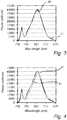
- the results of measurement runs are presented in table 1 below and in Figure 3 .
- Figure 3 shows the output power as a function of wavelength before and after engraving the light exit window 12.
- the solid curve 30 represents before laser engraving, and the dashed curve 31 represents after laser engraving.
- a second set of measurement runs have also been performed, for studying how the characteristics of the output light are affected by engraving 100 % of the total surface area of the outer surface S of the light exit window 12.
- the measurement runs were performed in the same manner as the previous measurement runs, except in view of the extent of engraving.
- the results of measurement runs are presented in table 2 below and in Figure 4 .
- Figure 4 shows the output power as a function of wavelength before and after engraving the light exit window 12.
- the solid curve 40 represents before laser engraving, and the dashed curve 41 represents after laser engraving.
- the tuning of color temperature is a fine tuning.
- the color temperature may be tuned 0.7-9.6 % depending on how much of the surface that is engraved.
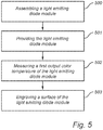
- a corresponding method for tuning the output color temperature of the lighting module 1 is illustrated in Figure 5 .
- the method comprises the steps of firstly assembling 500 the lighting module 1, secondly providing 501 the lighting module 1, thirdly measuring 502 a first output color temperature of the lighting module 1, and fourthly engraving 503 a surface of the lighting module 1.
- the color temperature of the output light from the LED module 1 may be tuned downwards to a lower color temperature.
- the tuning of the output color temperature may also be affected by the intensity/roughness of the engraving.
- the tuning of the output color temperature may be controlled by the amount of the surface area of the light exit window 12 that is engraved. In this case, the relation between the change in output color temperature and engraved area is expected to be linear.
- the color temperature of the lighting module 1 is increased by controlling or tuning the amount of scatter or reflection, for example with a laser engraved pattern.
- the light exit window 12 has predefined scattering properties.
- the light exit window 12 is a ceramic layer
- a modification of the porosity of the light exit window 12 provides for a modification of the scattering properties.
- An increase of the porosity of the light exit window 12 will lead to increased scattering, and this provides for an increase of light that is scattered back to the coating 13, being in this case a phosphor coating, resulting in a warmer color of the output light.
- a reduction of the amount of scattering will thus give a cooler color, i.e. a higher color temperature.
- the light exit window 12 may comprise a diffusing or partially reflecting layer (not shown) which may be applied on top of the light exit window 12. Removal of at least a part of this layer in a controlled way leads to an increase of the color temperature.
- a scattering glass layer or a scattering polymer coating may be provided on the light exit window 12 which is laser engraved, in accordance to e.g. a pattern, which leads to an increase the color temperature.
- the lighting module 1 By assembling the lighting module 1 before engraving of the light exit window 12, the lighting module 1 may be assembled at one location along a manufacturing line, and transported to another location for laser engraving. Since the lighting module 1 is already assembled, there is no risk for damaging any inner components of the lighting module 1 during the transportation.
- the final second output color temperature of the lighting module may be tuned based on a predetermined value. For example, it may be determined that each lighting module in a batch of lighting modules is to be tuned to a target color temperature of 2750 K. Depending on how much the measured first output color temperature for each lighting modules differs from the target color temperature, the lighting module may need tuning to different extents.
- the tuned second color temperature may be measured in order to verify that it corresponds to the target color temperature.
- the method may further comprise, subsequent to the engraving 503, measuring the output color temperature and compare the measured output color temperature with a predetermined target color temperature. If there is a difference between the measured output color temperature and the target color temperature, the method may comprise further steps of engraving and subsequent measuring of the output color temperature until the target color temperature is achieved.
- the light exit window 12 is engraved according to the above disclosed description. By engraving the outer surface S of the light exit window 12, the lighting module 1 does not need to be de-assembled before the engraving process.
- a sub-surface of the light exit window 12, i.e. a layer within the light exit window 12, may alternatively or additionally be engraved without the need for de-assembling of the lighting module 1 before the engraving process.
- any coating 13 arranged in the housing 11 may be protected from damaging during the engraving process.
- the method may further comprise arranging (not shown) a cover to the lighting module 1.
- the cover is arranged adjacent to the outer surface S of the light exit window 12.
- the outer surface S optionally comprising an injection moulded pattern, may be protected from e.g. dust or physical damage.
- the cover may also be engraved. For example, a visual pattern may be engraved in the cover subsequent to arranging the cover to the lighting module 1.
- the light exit window 12 may be injection moulded.
- a light exit window 12 may comprise an injection moulded pattern, such as a logotype.
- the injection moulded pattern may be negative or positive.
- the engraving of the light exit window 12 may be performed in the injection moulded pattern.
- lighting modules with an alumina and optionally glass window is one application. These lighting modules can be proximity, vicinity as well as remote phosphor modules.
- Other optical applications being based on the same principle may also be included, i.e. optical applications where light may be backscattered at an engraving in the light exit window, and where the backscattered light may be converted in the lighting module, by e.g. a coating, to another wavelength, thus modifying the light characteristics, in particular the color temperature, of the output light of the lighting module.
- the present invention relates to a method for tuning an output color temperature of a lighting module 1, said method comprising providing 501 said lighting module comprising a light exit window 12, and a light source 10 arranged to provide light having an optical path 101, 102, 103 through said light exit window 12, said lighting module having a first output color temperature; and engraving 503 a surface of said light exit window 12 such that the output color temperature of said lighting module is tuned to a second output color temperature.
- the present invention also relates to a lighting module 1, wherein a light exit window 12 of the lighting module is engraved such that the output color temperature of said lighting module is tuned.
- the lighting module may be of many different shapes and structures, such as having multiple LED chips or other lighting sources or being in the form of an array of light sources and/or housings sharing the same light exit window.
- the lighting module may be other types of lighting modules than LED modules, and may include other types of light sources.
- Non-limiting examples of other types of lighting modules are lighting bulbs, lighting tubes, and organic light emitting diode modules (OLED modules).
Landscapes
- Engineering & Computer Science (AREA)
- Physics & Mathematics (AREA)
- General Engineering & Computer Science (AREA)
- Spectroscopy & Molecular Physics (AREA)
- Microelectronics & Electronic Packaging (AREA)
- Optics & Photonics (AREA)
- Health & Medical Sciences (AREA)
- Toxicology (AREA)
- Non-Portable Lighting Devices Or Systems Thereof (AREA)
- Optical Filters (AREA)
- Illuminated Signs And Luminous Advertising (AREA)
- Led Device Packages (AREA)
Applications Claiming Priority (2)
| Application Number | Priority Date | Filing Date | Title |
|---|---|---|---|
| US201361776108P | 2013-03-11 | 2013-03-11 | |
| PCT/IB2014/059574 WO2014141030A1 (en) | 2013-03-11 | 2014-03-10 | A light emitting diode module with improved light characteristics |
Publications (2)
| Publication Number | Publication Date |
|---|---|
| EP2971935A1 EP2971935A1 (en) | 2016-01-20 |
| EP2971935B1 true EP2971935B1 (en) | 2018-07-04 |
Family
ID=50473713
Family Applications (1)
| Application Number | Title | Priority Date | Filing Date |
|---|---|---|---|
| EP14716411.5A Not-in-force EP2971935B1 (en) | 2013-03-11 | 2014-03-10 | A light emitting diode module with improved light characteristics |
Country Status (5)
| Country | Link |
|---|---|
| US (1) | US9746153B2 (enExample) |
| EP (1) | EP2971935B1 (enExample) |
| JP (1) | JP6396345B2 (enExample) |
| CN (1) | CN105074320B (enExample) |
| WO (1) | WO2014141030A1 (enExample) |
Families Citing this family (17)
| Publication number | Priority date | Publication date | Assignee | Title |
|---|---|---|---|---|
| WO2013186954A1 (ja) * | 2012-06-11 | 2013-12-19 | 日本電気株式会社 | 光源ユニット、投射型表示装置、照明器具及び光出射方法 |
| DE102012109806A1 (de) * | 2012-10-15 | 2014-04-17 | Osram Opto Semiconductors Gmbh | Strahlungsemittierendes Bauelement |
| CN103805196B (zh) * | 2014-02-27 | 2016-09-28 | 昆山开威电子有限公司 | 一种基于Ce:YAG晶片的复合结构及制作方法 |
| JP6654560B2 (ja) * | 2014-05-07 | 2020-02-26 | 株式会社小糸製作所 | 光源モジュールおよび車両用灯具 |
| US9748086B2 (en) | 2014-05-15 | 2017-08-29 | Excelitas Technologies Corp. | Laser driven sealed beam lamp |
| US10186416B2 (en) | 2014-05-15 | 2019-01-22 | Excelitas Technologies Corp. | Apparatus and a method for operating a variable pressure sealed beam lamp |
| CN105501108B (zh) * | 2014-10-08 | 2020-07-07 | 福特全球技术公司 | 具有点亮的车轮总成的车辆照明系统 |
| US9580650B1 (en) | 2014-12-25 | 2017-02-28 | DM Lighting Technologies Inc. | Method of manufacturing Ce:YAG polycrystalline phosphor |
| US10057973B2 (en) | 2015-05-14 | 2018-08-21 | Excelitas Technologies Corp. | Electrodeless single low power CW laser driven plasma lamp |
| US10008378B2 (en) * | 2015-05-14 | 2018-06-26 | Excelitas Technologies Corp. | Laser driven sealed beam lamp with improved stability |
| JP6583813B2 (ja) * | 2015-07-30 | 2019-10-02 | パナソニックIpマネジメント株式会社 | 光源および当該光源を用いた照明装置 |
| USD848054S1 (en) * | 2016-06-01 | 2019-05-07 | Fuzhou F&V Photographic Equipment Co., Ltd. | Spotlight |
| EP3737258B1 (en) * | 2018-01-10 | 2025-03-12 | Koninklijke Philips N.V. | Laser-enhanced optical element |
| KR102218345B1 (ko) * | 2019-01-23 | 2021-02-22 | 주식회사 지엘비젼 | 조명 장치 |
| US12000585B2 (en) * | 2019-08-07 | 2024-06-04 | Kyocera Corporation | Lighting device |
| JP7763622B2 (ja) | 2021-09-08 | 2025-11-04 | 新光電気工業株式会社 | セラミック組成物及びセラミック組成物の製造方法 |
| DE102023213188A1 (de) * | 2023-12-21 | 2025-06-26 | Carl Zeiss Smt Gmbh | Verfahren zum Schützen einer Kleberschicht vor Streustrahlung, optische Komponente und Anlage der Hableitertechnologie |
Family Cites Families (15)
| Publication number | Priority date | Publication date | Assignee | Title |
|---|---|---|---|---|
| JPH0383878A (ja) | 1989-08-25 | 1991-04-09 | Toshiba Corp | セラミックス装飾方法 |
| JPH1185075A (ja) * | 1997-09-03 | 1999-03-30 | Idec Izumi Corp | 表示装置 |
| JP5490407B2 (ja) | 2005-03-14 | 2014-05-14 | コーニンクレッカ フィリップス エヌ ヴェ | 多結晶セラミック構造の蛍光体、及び前記蛍光体を有する発光素子 |
| KR20070107261A (ko) | 2006-05-02 | 2007-11-07 | 삼성전자주식회사 | 광출사모듈 및 이를 갖는 표시장치 |
| CN2929456Y (zh) | 2006-07-06 | 2007-08-01 | 伟志智能有限公司 | 扩散型led照明光源 |
| JP2008273666A (ja) * | 2007-04-26 | 2008-11-13 | Toshiba Corp | 紙葉類取り出し装置 |
| US7942556B2 (en) * | 2007-06-18 | 2011-05-17 | Xicato, Inc. | Solid state illumination device |
| US7915627B2 (en) | 2007-10-17 | 2011-03-29 | Intematix Corporation | Light emitting device with phosphor wavelength conversion |
| KR100944008B1 (ko) | 2007-12-17 | 2010-02-24 | 삼성전기주식회사 | 백색 발광소자 및 그 제조방법 |
| US8427605B2 (en) * | 2008-09-23 | 2013-04-23 | Koninklijke Philips Electronics N.V. | Illumination device with electrical variable scattering element |
| KR101475045B1 (ko) | 2008-10-07 | 2014-12-23 | 엘지이노텍 주식회사 | 발광엠블럼 어셈블리 |
| CN101402860B (zh) | 2008-10-08 | 2011-06-15 | 天津理工大学 | 单基质单掺杂铝酸镧全色可调荧光体及制作方法 |
| US8882284B2 (en) * | 2010-03-03 | 2014-11-11 | Cree, Inc. | LED lamp or bulb with remote phosphor and diffuser configuration with enhanced scattering properties |
| US9500325B2 (en) * | 2010-03-03 | 2016-11-22 | Cree, Inc. | LED lamp incorporating remote phosphor with heat dissipation features |
| KR20130139938A (ko) * | 2010-10-05 | 2013-12-23 | 인터매틱스 코포레이션 | 포토루미네센스 파장 변환을 구비한 고체상태 발광 디바이스 및 표지판 |
-
2014
- 2014-03-10 CN CN201480013785.4A patent/CN105074320B/zh not_active Expired - Fee Related
- 2014-03-10 JP JP2015562464A patent/JP6396345B2/ja not_active Expired - Fee Related
- 2014-03-10 US US14/774,333 patent/US9746153B2/en not_active Expired - Fee Related
- 2014-03-10 EP EP14716411.5A patent/EP2971935B1/en not_active Not-in-force
- 2014-03-10 WO PCT/IB2014/059574 patent/WO2014141030A1/en not_active Ceased
Non-Patent Citations (1)
| Title |
|---|
| None * |
Also Published As
| Publication number | Publication date |
|---|---|
| JP6396345B2 (ja) | 2018-09-26 |
| CN105074320B (zh) | 2019-05-14 |
| WO2014141030A1 (en) | 2014-09-18 |
| CN105074320A (zh) | 2015-11-18 |
| US9746153B2 (en) | 2017-08-29 |
| US20160025294A1 (en) | 2016-01-28 |
| JP2016519829A (ja) | 2016-07-07 |
| EP2971935A1 (en) | 2016-01-20 |
Similar Documents
| Publication | Publication Date | Title |
|---|---|---|
| EP2971935B1 (en) | A light emitting diode module with improved light characteristics | |
| EP3025380B1 (en) | Flip-chip side emitting led | |
| US8851694B2 (en) | Semiconductor light source apparatus | |
| US8222054B2 (en) | LED light source and chromaticity adjustment method for LED light source | |
| US9366395B2 (en) | Optical element, optoelectronic component and method for the production thereof | |
| TWI725012B (zh) | 具改善的色彩一致性之光源組件 | |
| US7909476B2 (en) | Light source module of light emitting diode | |
| KR101908449B1 (ko) | 비대칭 방사 패턴을 가진 발광 디바이스 및 제조 방법 | |
| KR101318913B1 (ko) | 균일한 색 분포를 위해 설계된 색변환층을 갖는 led 모듈 | |
| JP2013016868A (ja) | Ledパッケージにおけるテクスチャード加工された封止体表面 | |
| KR20110111390A (ko) | 향상된 색 품질을 가진 반도체 조명 시스템 | |
| JP2009193994A (ja) | Led光源およびその色度調整方法 | |
| KR20140097346A (ko) | 필라멘트 효과를 생성하기 위한 led 램프 상의 측면 발광 가이드파이프 기술 | |
| KR20160036489A (ko) | 발광 장치 | |
| KR20170068518A (ko) | 네오디뮴-불소 재료를 채용하는 led 장치 | |
| JP2009193995A (ja) | Led光源およびその色度調整方法 | |
| TWI639255B (zh) | 在一晶片級封裝發光二極體之基板中的塑形空腔 | |
| CN113130721B (zh) | 采用使用多种钕和氟化合物的可调滤色的led设备 | |
| KR102131771B1 (ko) | 발광 소자 패키지 및 이를 포함하는 조명 장치 | |
| US20110062454A1 (en) | Light emitting device having remotely located light scattering material | |
| US20190284472A1 (en) | Polycrystalline phosphor film, preparation method therefor, and vehicle lamp device using same | |
| JP2015097260A (ja) | 照明装置 | |
| JP5291162B2 (ja) | 発光装置およびその製造方法 | |
| WO2011032309A1 (en) | Light emitting device having remotely located light scattering material | |
| JP2008010748A (ja) | 発光装置およびその製造方法 |
Legal Events
| Date | Code | Title | Description |
|---|---|---|---|
| PUAI | Public reference made under article 153(3) epc to a published international application that has entered the european phase |
Free format text: ORIGINAL CODE: 0009012 |
|
| 17P | Request for examination filed |
Effective date: 20151012 |
|
| AK | Designated contracting states |
Kind code of ref document: A1 Designated state(s): AL AT BE BG CH CY CZ DE DK EE ES FI FR GB GR HR HU IE IS IT LI LT LU LV MC MK MT NL NO PL PT RO RS SE SI SK SM TR |
|
| AX | Request for extension of the european patent |
Extension state: BA ME |
|
| DAX | Request for extension of the european patent (deleted) | ||
| RAP1 | Party data changed (applicant data changed or rights of an application transferred) |
Owner name: PHILIPS LIGHTING HOLDING B.V. |
|
| RIN1 | Information on inventor provided before grant (corrected) |
Inventor name: JAGT, HENDRIK, JOHANNES, BOUDEWIJN Inventor name: DIJKEN, DURANDUS, KORNELIUS Inventor name: ASADI, KAMAL Inventor name: SANDERS, RENATUS, HENDRICUS, MARIA Inventor name: KROES, HANS Inventor name: YU, JIANGHONG |
|
| REG | Reference to a national code |
Ref country code: DE Ref legal event code: R079 Ref document number: 602014027842 Country of ref document: DE Free format text: PREVIOUS MAIN CLASS: F21K0099000000 Ipc: H05B0033080000 |
|
| GRAP | Despatch of communication of intention to grant a patent |
Free format text: ORIGINAL CODE: EPIDOSNIGR1 |
|
| STAA | Information on the status of an ep patent application or granted ep patent |
Free format text: STATUS: GRANT OF PATENT IS INTENDED |
|
| RIC1 | Information provided on ipc code assigned before grant |
Ipc: B29L 11/00 20060101ALN20180110BHEP Ipc: F21V 3/04 20180101ALI20180110BHEP Ipc: B29C 59/16 20060101ALI20180110BHEP Ipc: F21K 9/62 20160101ALI20180110BHEP Ipc: F21K 9/64 20160101ALI20180110BHEP Ipc: F21Y 115/10 20160101ALN20180110BHEP Ipc: H05B 33/08 20060101AFI20180110BHEP |
|
| INTG | Intention to grant announced |
Effective date: 20180130 |
|
| RIN1 | Information on inventor provided before grant (corrected) |
Inventor name: YU, JIANGHONG Inventor name: SANDERS, RENATUS, HENDRICUS, MARIA Inventor name: ASADI, KAMAL Inventor name: DIJKEN, DURANDUS, KORNELIUS Inventor name: KROES, HANS Inventor name: JAGT, HENDRIK, JOHANNES, BOUDEWIJN |
|
| GRAS | Grant fee paid |
Free format text: ORIGINAL CODE: EPIDOSNIGR3 |
|
| GRAA | (expected) grant |
Free format text: ORIGINAL CODE: 0009210 |
|
| STAA | Information on the status of an ep patent application or granted ep patent |
Free format text: STATUS: THE PATENT HAS BEEN GRANTED |
|
| AK | Designated contracting states |
Kind code of ref document: B1 Designated state(s): AL AT BE BG CH CY CZ DE DK EE ES FI FR GB GR HR HU IE IS IT LI LT LU LV MC MK MT NL NO PL PT RO RS SE SI SK SM TR |
|
| REG | Reference to a national code |
Ref country code: GB Ref legal event code: FG4D |
|
| REG | Reference to a national code |
Ref country code: CH Ref legal event code: EP |
|
| REG | Reference to a national code |
Ref country code: AT Ref legal event code: REF Ref document number: 1015903 Country of ref document: AT Kind code of ref document: T Effective date: 20180715 |
|
| REG | Reference to a national code |
Ref country code: IE Ref legal event code: FG4D |
|
| REG | Reference to a national code |
Ref country code: DE Ref legal event code: R096 Ref document number: 602014027842 Country of ref document: DE |
|
| REG | Reference to a national code |
Ref country code: NL Ref legal event code: MP Effective date: 20180704 |
|
| REG | Reference to a national code |
Ref country code: LT Ref legal event code: MG4D |
|
| RAP2 | Party data changed (patent owner data changed or rights of a patent transferred) |
Owner name: PHILIPS LIGHTING HOLDING B.V. |
|
| REG | Reference to a national code |
Ref country code: AT Ref legal event code: MK05 Ref document number: 1015903 Country of ref document: AT Kind code of ref document: T Effective date: 20180704 |
|
| PG25 | Lapsed in a contracting state [announced via postgrant information from national office to epo] |
Ref country code: NL Free format text: LAPSE BECAUSE OF FAILURE TO SUBMIT A TRANSLATION OF THE DESCRIPTION OR TO PAY THE FEE WITHIN THE PRESCRIBED TIME-LIMIT Effective date: 20180704 |
|
| PG25 | Lapsed in a contracting state [announced via postgrant information from national office to epo] |
Ref country code: RS Free format text: LAPSE BECAUSE OF FAILURE TO SUBMIT A TRANSLATION OF THE DESCRIPTION OR TO PAY THE FEE WITHIN THE PRESCRIBED TIME-LIMIT Effective date: 20180704 Ref country code: IS Free format text: LAPSE BECAUSE OF FAILURE TO SUBMIT A TRANSLATION OF THE DESCRIPTION OR TO PAY THE FEE WITHIN THE PRESCRIBED TIME-LIMIT Effective date: 20181104 Ref country code: PL Free format text: LAPSE BECAUSE OF FAILURE TO SUBMIT A TRANSLATION OF THE DESCRIPTION OR TO PAY THE FEE WITHIN THE PRESCRIBED TIME-LIMIT Effective date: 20180704 Ref country code: LT Free format text: LAPSE BECAUSE OF FAILURE TO SUBMIT A TRANSLATION OF THE DESCRIPTION OR TO PAY THE FEE WITHIN THE PRESCRIBED TIME-LIMIT Effective date: 20180704 Ref country code: AT Free format text: LAPSE BECAUSE OF FAILURE TO SUBMIT A TRANSLATION OF THE DESCRIPTION OR TO PAY THE FEE WITHIN THE PRESCRIBED TIME-LIMIT Effective date: 20180704 Ref country code: GR Free format text: LAPSE BECAUSE OF FAILURE TO SUBMIT A TRANSLATION OF THE DESCRIPTION OR TO PAY THE FEE WITHIN THE PRESCRIBED TIME-LIMIT Effective date: 20181005 Ref country code: NO Free format text: LAPSE BECAUSE OF FAILURE TO SUBMIT A TRANSLATION OF THE DESCRIPTION OR TO PAY THE FEE WITHIN THE PRESCRIBED TIME-LIMIT Effective date: 20181004 Ref country code: FI Free format text: LAPSE BECAUSE OF FAILURE TO SUBMIT A TRANSLATION OF THE DESCRIPTION OR TO PAY THE FEE WITHIN THE PRESCRIBED TIME-LIMIT Effective date: 20180704 Ref country code: SE Free format text: LAPSE BECAUSE OF FAILURE TO SUBMIT A TRANSLATION OF THE DESCRIPTION OR TO PAY THE FEE WITHIN THE PRESCRIBED TIME-LIMIT Effective date: 20180704 Ref country code: CZ Free format text: LAPSE BECAUSE OF FAILURE TO SUBMIT A TRANSLATION OF THE DESCRIPTION OR TO PAY THE FEE WITHIN THE PRESCRIBED TIME-LIMIT Effective date: 20180704 Ref country code: BG Free format text: LAPSE BECAUSE OF FAILURE TO SUBMIT A TRANSLATION OF THE DESCRIPTION OR TO PAY THE FEE WITHIN THE PRESCRIBED TIME-LIMIT Effective date: 20181004 |
|
| PG25 | Lapsed in a contracting state [announced via postgrant information from national office to epo] |
Ref country code: LV Free format text: LAPSE BECAUSE OF FAILURE TO SUBMIT A TRANSLATION OF THE DESCRIPTION OR TO PAY THE FEE WITHIN THE PRESCRIBED TIME-LIMIT Effective date: 20180704 Ref country code: ES Free format text: LAPSE BECAUSE OF FAILURE TO SUBMIT A TRANSLATION OF THE DESCRIPTION OR TO PAY THE FEE WITHIN THE PRESCRIBED TIME-LIMIT Effective date: 20180704 Ref country code: HR Free format text: LAPSE BECAUSE OF FAILURE TO SUBMIT A TRANSLATION OF THE DESCRIPTION OR TO PAY THE FEE WITHIN THE PRESCRIBED TIME-LIMIT Effective date: 20180704 Ref country code: AL Free format text: LAPSE BECAUSE OF FAILURE TO SUBMIT A TRANSLATION OF THE DESCRIPTION OR TO PAY THE FEE WITHIN THE PRESCRIBED TIME-LIMIT Effective date: 20180704 |
|
| RAP2 | Party data changed (patent owner data changed or rights of a patent transferred) |
Owner name: SIGNIFY HOLDING B.V. |
|
| REG | Reference to a national code |
Ref country code: DE Ref legal event code: R097 Ref document number: 602014027842 Country of ref document: DE |
|
| PG25 | Lapsed in a contracting state [announced via postgrant information from national office to epo] |
Ref country code: IT Free format text: LAPSE BECAUSE OF FAILURE TO SUBMIT A TRANSLATION OF THE DESCRIPTION OR TO PAY THE FEE WITHIN THE PRESCRIBED TIME-LIMIT Effective date: 20180704 Ref country code: RO Free format text: LAPSE BECAUSE OF FAILURE TO SUBMIT A TRANSLATION OF THE DESCRIPTION OR TO PAY THE FEE WITHIN THE PRESCRIBED TIME-LIMIT Effective date: 20180704 Ref country code: EE Free format text: LAPSE BECAUSE OF FAILURE TO SUBMIT A TRANSLATION OF THE DESCRIPTION OR TO PAY THE FEE WITHIN THE PRESCRIBED TIME-LIMIT Effective date: 20180704 |
|
| PLBE | No opposition filed within time limit |
Free format text: ORIGINAL CODE: 0009261 |
|
| STAA | Information on the status of an ep patent application or granted ep patent |
Free format text: STATUS: NO OPPOSITION FILED WITHIN TIME LIMIT |
|
| PG25 | Lapsed in a contracting state [announced via postgrant information from national office to epo] |
Ref country code: SK Free format text: LAPSE BECAUSE OF FAILURE TO SUBMIT A TRANSLATION OF THE DESCRIPTION OR TO PAY THE FEE WITHIN THE PRESCRIBED TIME-LIMIT Effective date: 20180704 Ref country code: SM Free format text: LAPSE BECAUSE OF FAILURE TO SUBMIT A TRANSLATION OF THE DESCRIPTION OR TO PAY THE FEE WITHIN THE PRESCRIBED TIME-LIMIT Effective date: 20180704 Ref country code: DK Free format text: LAPSE BECAUSE OF FAILURE TO SUBMIT A TRANSLATION OF THE DESCRIPTION OR TO PAY THE FEE WITHIN THE PRESCRIBED TIME-LIMIT Effective date: 20180704 |
|
| 26N | No opposition filed |
Effective date: 20190405 |
|
| PG25 | Lapsed in a contracting state [announced via postgrant information from national office to epo] |
Ref country code: SI Free format text: LAPSE BECAUSE OF FAILURE TO SUBMIT A TRANSLATION OF THE DESCRIPTION OR TO PAY THE FEE WITHIN THE PRESCRIBED TIME-LIMIT Effective date: 20180704 |
|
| PG25 | Lapsed in a contracting state [announced via postgrant information from national office to epo] |
Ref country code: MC Free format text: LAPSE BECAUSE OF FAILURE TO SUBMIT A TRANSLATION OF THE DESCRIPTION OR TO PAY THE FEE WITHIN THE PRESCRIBED TIME-LIMIT Effective date: 20180704 |
|
| REG | Reference to a national code |
Ref country code: CH Ref legal event code: PL |
|
| REG | Reference to a national code |
Ref country code: DE Ref legal event code: R079 Ref document number: 602014027842 Country of ref document: DE Free format text: PREVIOUS MAIN CLASS: H05B0033080000 Ipc: H05B0045000000 |
|
| PG25 | Lapsed in a contracting state [announced via postgrant information from national office to epo] |
Ref country code: LU Free format text: LAPSE BECAUSE OF NON-PAYMENT OF DUE FEES Effective date: 20190310 |
|
| REG | Reference to a national code |
Ref country code: BE Ref legal event code: MM Effective date: 20190331 |
|
| PG25 | Lapsed in a contracting state [announced via postgrant information from national office to epo] |
Ref country code: IE Free format text: LAPSE BECAUSE OF NON-PAYMENT OF DUE FEES Effective date: 20190310 Ref country code: LI Free format text: LAPSE BECAUSE OF NON-PAYMENT OF DUE FEES Effective date: 20190331 Ref country code: CH Free format text: LAPSE BECAUSE OF NON-PAYMENT OF DUE FEES Effective date: 20190331 |
|
| PG25 | Lapsed in a contracting state [announced via postgrant information from national office to epo] |
Ref country code: BE Free format text: LAPSE BECAUSE OF NON-PAYMENT OF DUE FEES Effective date: 20190331 |
|
| PG25 | Lapsed in a contracting state [announced via postgrant information from national office to epo] |
Ref country code: TR Free format text: LAPSE BECAUSE OF FAILURE TO SUBMIT A TRANSLATION OF THE DESCRIPTION OR TO PAY THE FEE WITHIN THE PRESCRIBED TIME-LIMIT Effective date: 20180704 |
|
| PGFP | Annual fee paid to national office [announced via postgrant information from national office to epo] |
Ref country code: GB Payment date: 20200327 Year of fee payment: 7 |
|
| PG25 | Lapsed in a contracting state [announced via postgrant information from national office to epo] |
Ref country code: PT Free format text: LAPSE BECAUSE OF FAILURE TO SUBMIT A TRANSLATION OF THE DESCRIPTION OR TO PAY THE FEE WITHIN THE PRESCRIBED TIME-LIMIT Effective date: 20181104 Ref country code: MT Free format text: LAPSE BECAUSE OF NON-PAYMENT OF DUE FEES Effective date: 20190310 |
|
| PGFP | Annual fee paid to national office [announced via postgrant information from national office to epo] |
Ref country code: FR Payment date: 20200326 Year of fee payment: 7 |
|
| PGFP | Annual fee paid to national office [announced via postgrant information from national office to epo] |
Ref country code: DE Payment date: 20200330 Year of fee payment: 7 |
|
| PG25 | Lapsed in a contracting state [announced via postgrant information from national office to epo] |
Ref country code: CY Free format text: LAPSE BECAUSE OF FAILURE TO SUBMIT A TRANSLATION OF THE DESCRIPTION OR TO PAY THE FEE WITHIN THE PRESCRIBED TIME-LIMIT Effective date: 20180704 |
|
| PG25 | Lapsed in a contracting state [announced via postgrant information from national office to epo] |
Ref country code: HU Free format text: LAPSE BECAUSE OF FAILURE TO SUBMIT A TRANSLATION OF THE DESCRIPTION OR TO PAY THE FEE WITHIN THE PRESCRIBED TIME-LIMIT; INVALID AB INITIO Effective date: 20140310 |
|
| REG | Reference to a national code |
Ref country code: DE Ref legal event code: R119 Ref document number: 602014027842 Country of ref document: DE |
|
| GBPC | Gb: european patent ceased through non-payment of renewal fee |
Effective date: 20210310 |
|
| PG25 | Lapsed in a contracting state [announced via postgrant information from national office to epo] |
Ref country code: DE Free format text: LAPSE BECAUSE OF NON-PAYMENT OF DUE FEES Effective date: 20211001 Ref country code: FR Free format text: LAPSE BECAUSE OF NON-PAYMENT OF DUE FEES Effective date: 20210331 Ref country code: GB Free format text: LAPSE BECAUSE OF NON-PAYMENT OF DUE FEES Effective date: 20210310 |
|
| PG25 | Lapsed in a contracting state [announced via postgrant information from national office to epo] |
Ref country code: MK Free format text: LAPSE BECAUSE OF FAILURE TO SUBMIT A TRANSLATION OF THE DESCRIPTION OR TO PAY THE FEE WITHIN THE PRESCRIBED TIME-LIMIT Effective date: 20180704 |