EP2962169B1 - Système et procédé de gestion thermique dans un dispositif informatique portable en utilisant des valeurs de résistance thermique pour prédire des niveaux de puissance optimaux - Google Patents
Système et procédé de gestion thermique dans un dispositif informatique portable en utilisant des valeurs de résistance thermique pour prédire des niveaux de puissance optimaux Download PDFInfo
- Publication number
- EP2962169B1 EP2962169B1 EP14711648.7A EP14711648A EP2962169B1 EP 2962169 B1 EP2962169 B1 EP 2962169B1 EP 14711648 A EP14711648 A EP 14711648A EP 2962169 B1 EP2962169 B1 EP 2962169B1
- Authority
- EP
- European Patent Office
- Prior art keywords
- temperature
- pcd
- thermal
- component
- power supply
- Prior art date
- Legal status (The legal status is an assumption and is not a legal conclusion. Google has not performed a legal analysis and makes no representation as to the accuracy of the status listed.)
- Not-in-force
Links
Images


Classifications
-
- G—PHYSICS
- G06—COMPUTING; CALCULATING OR COUNTING
- G06F—ELECTRIC DIGITAL DATA PROCESSING
- G06F1/00—Details not covered by groups G06F3/00 - G06F13/00 and G06F21/00
- G06F1/26—Power supply means, e.g. regulation thereof
-
- G—PHYSICS
- G06—COMPUTING; CALCULATING OR COUNTING
- G06F—ELECTRIC DIGITAL DATA PROCESSING
- G06F1/00—Details not covered by groups G06F3/00 - G06F13/00 and G06F21/00
- G06F1/16—Constructional details or arrangements
- G06F1/20—Cooling means
- G06F1/203—Cooling means for portable computers, e.g. for laptops
-
- G—PHYSICS
- G06—COMPUTING; CALCULATING OR COUNTING
- G06F—ELECTRIC DIGITAL DATA PROCESSING
- G06F1/00—Details not covered by groups G06F3/00 - G06F13/00 and G06F21/00
- G06F1/16—Constructional details or arrangements
- G06F1/20—Cooling means
- G06F1/206—Cooling means comprising thermal management
-
- G—PHYSICS
- G06—COMPUTING; CALCULATING OR COUNTING
- G06F—ELECTRIC DIGITAL DATA PROCESSING
- G06F1/00—Details not covered by groups G06F3/00 - G06F13/00 and G06F21/00
- G06F1/26—Power supply means, e.g. regulation thereof
- G06F1/32—Means for saving power
- G06F1/3203—Power management, i.e. event-based initiation of a power-saving mode
- G06F1/3234—Power saving characterised by the action undertaken
- G06F1/324—Power saving characterised by the action undertaken by lowering clock frequency
-
- G—PHYSICS
- G06—COMPUTING; CALCULATING OR COUNTING
- G06F—ELECTRIC DIGITAL DATA PROCESSING
- G06F1/00—Details not covered by groups G06F3/00 - G06F13/00 and G06F21/00
- G06F1/26—Power supply means, e.g. regulation thereof
- G06F1/32—Means for saving power
- G06F1/3203—Power management, i.e. event-based initiation of a power-saving mode
- G06F1/3234—Power saving characterised by the action undertaken
- G06F1/3296—Power saving characterised by the action undertaken by lowering the supply or operating voltage
-
- G—PHYSICS
- G06—COMPUTING; CALCULATING OR COUNTING
- G06F—ELECTRIC DIGITAL DATA PROCESSING
- G06F2119/00—Details relating to the type or aim of the analysis or the optimisation
- G06F2119/08—Thermal analysis or thermal optimisation
-
- Y—GENERAL TAGGING OF NEW TECHNOLOGICAL DEVELOPMENTS; GENERAL TAGGING OF CROSS-SECTIONAL TECHNOLOGIES SPANNING OVER SEVERAL SECTIONS OF THE IPC; TECHNICAL SUBJECTS COVERED BY FORMER USPC CROSS-REFERENCE ART COLLECTIONS [XRACs] AND DIGESTS
- Y02—TECHNOLOGIES OR APPLICATIONS FOR MITIGATION OR ADAPTATION AGAINST CLIMATE CHANGE
- Y02D—CLIMATE CHANGE MITIGATION TECHNOLOGIES IN INFORMATION AND COMMUNICATION TECHNOLOGIES [ICT], I.E. INFORMATION AND COMMUNICATION TECHNOLOGIES AIMING AT THE REDUCTION OF THEIR OWN ENERGY USE
- Y02D10/00—Energy efficient computing, e.g. low power processors, power management or thermal management
Definitions
- PCDs Portable computing devices
- PDAs portable digital assistants
- game consoles portable game consoles
- palmtop computers portable electronic devices
- PCDs typically do not have active cooling devices, like fans, which are often found in larger computing devices such as laptop and desktop computers. Instead of using fans, PCDs may rely on the spatial arrangement of electronic packaging so that two or more active and heat producing components are not positioned proximally to one another. Many PCDs may also rely on passive cooling devices, such as heat sinks, to manage thermal energy among the electronic components which collectively form a respective PCD.
- active cooling devices like fans
- PCDs are typically limited in size and, therefore, room for components within a PCD often comes at a premium.
- some systems and methods may monitor temperature sensors to recognize that thermal thresholds have been exceeded before dynamically scaling voltage and/or frequency ("DVFS") settings in order to "dial back" power consumption of cores to reduce thermal energy generation.
- DVFS dynamically scaling voltage and/or frequency
- embodiments of the existing solutions may reduce power levels to cores one bin at a time or may rely on the recognition of use cases to jump down multiple bins at a time in an effort to more quickly stabilize thermal energy generation.
- the temperature sensors are queried again to determine if the previous power level adjustments produced the hoped-for reduction in thermal energy generation. If not, more adjustments are made and the loop continues until thermal energy levels are acceptable.
- US 2012/179303 A1 relates to a method and system for managing thermal policies of a portable computing device.
- thermo energy management in a portable computing device based on power level calculations
- temperature thresholds associated with various components in the PCD such as, but not limited to, die junction temperatures and package on package (“PoP") memory temperatures limits the extent to which the performance capabilities of the PCD can be exploited.
- PoP package on package
- an adjusted power supply level may be calculated using the instantaneous R INST value and a target operating temperature in place of the T INST value in the above equation.
- the adjusted power supply calculation may then be used to determine the necessary amount of voltage and/or frequency scaling required to keep the component within acceptable thermal bounds.
- embodiments of the above systems and methods may be used to mitigate thermal energy generation by reducing power supply levels in response to an elevated temperature measurement or, alternatively, may be used to authorize an increase in power supply levels (and, thus, an increase in thermal energy generation) in response to the recognition that additional thermal headroom is available.
- an “application” may also include files having executable content, such as: object code, scripts, byte code, markup language files, and patches.
- an “application” referred to herein may also include files that are not executable in nature, such as documents that may need to be opened or other data files that need to be accessed.
- a component may be, but is not limited to being, a process running on a processor, a processor, an object, an executable, a thread of execution, a program, and/or a computer.
- an application running on a computing device and the computing device may be a component.
- One or more components may reside within a process and/or thread of execution, and a component may be localized on one computer and/or distributed between two or more computers.
- these components may execute from various computer readable media having various data structures stored thereon.
- the components may communicate by way of local and/or remote processes such as in accordance with a signal having one or more data packets (e.g ., data from one component interacting with another component in a local system, distributed system, and/or across a network such as the Internet with other systems by way of the signal).
- CPU central processing unit
- DSP digital signal processor
- GPU graphical processing unit
- chips are used interchangeably.
- a CPU, DSP, GPU or a chip may be comprised of one or more distinct processing components generally referred to herein as “core(s).”
- core distinct processing components generally referred to herein as “core(s).”
- a CPU, DSP, GPU, chip or core is a functional component within a PCD that consumes various levels of power to operate at various levels of functional efficiency, one of ordinary skill in the art will recognize that the use of these terms does not limit the application of the disclosed embodiments, or their equivalents, to the context of processing components within a PCD.
- thermal management policies may be applied to any functional component within a PCD including, but not limited to, a modem, a camera, a wireless network interface controller ("WNIC"), a display, a video encoder, a peripheral device, a battery, etc.
- WNIC wireless network interface controller
- thermo and “thermal energy” may be used in association with a device or component capable of generating or dissipating energy that can be measured in units of "temperature.” Consequently, it will further be understood that the term “temperature,” with reference to some standard value, envisions any measurement that may be indicative of the relative warmth, or absence of heat, of a “thermal energy” generating device or component. For example, the "temperature” of two components is the same when the two components are in “thermal” equilibrium.
- a “processing component” or “thermal energy generating component” or “thermal aggressor” may be, but is not limited to, a central processing unit, a graphical processing unit, a core, a main core, a sub-core, a processing area, a hardware engine, etc. or any component residing within, or external to, an integrated circuit within a portable computing device.
- thermo load thermal load
- thermal distribution thermo distribution
- thermal signature thermo processing load
- thermo mitigation technique(s), thermal policies
- thermal management thermal energy generation
- thermal mitigation measure(s) throttling to a performance level
- any of the terms listed in this paragraph may serve to describe hardware and/or software operable to increase performance at the expense of thermal energy generation, decrease thermal energy generation at the expense of performance, or alternate between such goals.
- PCD portable computing device
- 3G third generation
- 4G fourth generation
- a PCD may be a cellular telephone, a satellite telephone, a pager, a PDA, a smartphone, a navigation device, a smartbook or reader, a media player, a combination of the aforementioned devices, a laptop computer with a wireless connection, among others.
- Efficient management of thermal energy generation in a PCD can be accomplished by using one or more sensor measurements that correlate with the temperatures of silicon junctions in core(s) in combination with an instantaneous thermal resistance value of the core(s).
- exemplary embodiments of the systems and methods are described herein in the context of temperature measurements associated with silicon junctions of cores, it will be understood that alternative embodiments may use temperature measurements and thermal resistance values associated with other components in a PCD. That is, although exemplary embodiments of thermal management methods that use predicted power level settings are described herein in the context of cores within a central processing unit (“CPU"), application of such thermal management methodologies are not limited to cores within a CPU.
- CPU central processing unit
- thermal management methods that use predicted power level settings may be extended to any component that may reside within a system on a chip (“SoC”) and be operable at multiple performance levels such as, but not limited to, a graphical processing unit (“GPU”), a modem processor, a camera, etc. Further, it is envisioned that a thermal management algorithm that predicts optimum power level settings from instantaneous thermal resistance values may be leveraged individually on any component within a SoC that may be operated at multiple performance levels.
- SoC system on a chip
- a maximum operating temperature ("T MAX ”) for silicon junctions of a core are empirically determined and then used to define a temperature threshold against which power levels for the core may be controlled.
- T MAX maximum operating temperature
- exposure of the junctions to operating temperatures in excess of a maximum operating temperature may cause damage to, or outright failure of, a processing component such as a core.
- thermal mitigation solutions may be employed to reduce the amount of thermal energy that is being generated by the core and/or other thermally aggressive components physically near the core.
- T INST exceeds a threshold associated with T MAX or other thermal threshold
- thermal mitigation may be necessary.
- T INST the temperature of the exemplary core
- P L the leakage power
- P SUPP the power being supplied to the core
- embodiments of the systems and methods may calculate a new P SUPP level, i.e. an optimum P SUPP for reducing thermal energy generation, by solving for P SUPP per equation (1) above.
- a new P SUPP level i.e. an optimum P SUPP for reducing thermal energy generation
- the systems and methods may substitute a desired temperature value for T INST in equation (1) and solve for a new P SUPP that would cause the T INST to reduce to the desired level.
- a targeted adjustment of voltage and/or frequency settings may be implemented to reduce the power supply to the optimum level for mitigating thermal energy generation.
- the optimum power level is calculated based on the real-time conditions, it is envisioned that the iterative process of making incremental power adjustments based on temperature measurements may be reduced or eliminated to a point that provides for a quicker thermal stabilization of the PCD.
- a system and method for thermal management by power level prediction may leverage means for throttling a core down or up, as the case may warrant, to the optimum performance level.
- throttling strategies are various methods, applications and/or algorithms that may be employed by the PCD to increase or decrease its performance through adjustment of hardware and/or software parameters, such as the clock speed of a central processing unit ("CPU") or the like.
- Certain throttling strategies may increase performance of a PCD at the expense of increased thermal energy generation; however, certain other throttling strategies may mitigate a detrimental rise in operating temperature by reducing PCD performance.
- An exemplary throttling method that may be leveraged by a thermal management policy is a dynamic voltage and frequency scaling ("DVFS”) method, described in more detail relative to FIG. 5 .
- DVFS dynamic voltage and frequency scaling
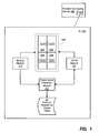
- FIG. 1 is a functional block diagram illustrating an embodiment of an on-chip system 102 for implementing in a portable computing device ("PCD") 100 thermal management methodologies that use thermal resistance values to predict optimum power level settings.
- the on-chip system 102 may leverage various sensors 157 for measuring temperatures associated with various components such as cores 222, 224, 226, 228.
- the QoS experienced by a user of the PCD 100 may be optimized while avoiding thermal degradation of junctions or other aspects.
- the system employs three main modules which, in some embodiments, may be contained in a pair of modules or a single module: (1) a monitor module 114 for polling temperature sensors 157 and monitoring power supply levels to the cores 222, 224, 226, 228; (2) a power level prediction (“PLP") module 101 for analyzing temperature readings and power supply levels provided by the monitor module 114, calculating and tracking the instantaneous thermal resistance values of the cores 222, 224, 226, 228, and determining optimum power level settings for the cores 222, 224, 226, 228 based on targeted operating temperatures; and (3) a DVFS module 26 for implementing power level adjustments on individual processing components according to instructions received from PLP module 101.
- a monitor module 114 for polling temperature sensors 157 and monitoring power supply levels to the cores 222, 224, 226, 228
- PLP power level prediction
- a DVFS module 26 for implementing power level adjustments on individual processing components according to instructions received from PLP module 101.
- an embodiment of the systems and methods may periodically poll the sensors 157A, which may be associated with silicon junctions of cores 222, 224, 226, 228, and provide the polled temperature data to the PLP module 101.
- the monitor module 114 may also monitor the power levels being supplied to the cores 222, 224, 226 , 228 and provide that data to PLP module 101 as well.
- the PLP module 101 may calculate a thermal resistance value according to the formulas provided and explained above.
- the PLP module 101 may store, either permanently or temporarily, the thermal resistance values in a thermal resistance values ("TRV") table 24.
- TRV thermal resistance values
- the PLP 101 may be alerted.
- the PLP module 101 may be triggered to calculate a new power level setting based on a target operating temperature that is within the limits delineated by the temperature threshold, according to the formulas provided and explained above.
- the new power level settings may be supplied to the DVFS module 26 and voltage and/or frequency settings adjusted based on the new power level setting.
- certain embodiments may recognize the instantaneous temperature levels are below a maximum threshold, thereby indicating available thermal headroom. Such embodiments may be triggered to calculate new power level settings that increase thermal energy generation and provide improved QoS without causing risking thermal degradation of processing components or other components.
- FIG. 2 is a functional block diagram illustrating an exemplary, non-limiting aspect of the PCD 100 in the form of a wireless telephone for implementing methods and systems for thermal management using thermal resistance values to predict optimum power level settings.
- the PCD 100 includes an on-chip system 102 that includes a multi-core central processing unit ("CPU") 110 and an analog signal processor 126 that are coupled together.
- the CPU 110 may comprise a zeroth core 222, a first core 224, and an Nth core 230 as understood by one of ordinary skill in the art.
- a digital signal processor may also be employed as understood by one of ordinary skill in the art.
- the dynamic voltage and frequency scaling (“DVFS") module 26 may be responsible for implementing throttling techniques to individual processing components, such as cores 222, 224, 230 to help a PCD 100 optimize its power level and maintain a high level of functionality without detrimentally exceeding certain temperature thresholds.
- DVFS dynamic voltage and frequency scaling
- the monitor module 114 communicates with multiple operational sensors (e.g., thermal sensors 157A, 157B) distributed throughout the on-chip system 102 and with the CPU 110 of the PCD 100 as well as with the PLP module 101.
- monitor module 114 may also monitor skin temperature sensors 157C for temperature readings associated with a touch temperature of PCD 100 and/or an ambient temperature ("T A ") to which PCD 100 is exposed.
- monitor module 114 may infer touch temperatures or ambient temperatures based on a likely delta with readings taken by on chip temperature sensors 157A, 157B.
- the PLP module 101 may work with the monitor module 114 to identify temperature thresholds that have been exceeded and instruct the application of throttling strategies to identified components within chip 102 in an effort to reduce the temperatures or, in other scenarios, allow for an increase in the temperatures.
- a display controller 128 and a touch screen controller 130 are coupled to the digital signal processor 110.
- a touch screen display 132 external to the on-chip system 102 is coupled to the display controller 128 and the touch screen controller 130.
- PCD 100 may further include a video encoder 134, e.g., a phase-alternating line (“PAL”) encoder, a sequential educational memoire (“SECAM”) encoder, a national television system(s) committee (“NTSC”) encoder or any other type of video encoder 134.
- the video encoder 134 is coupled to the multi-core central processing unit (“CPU") 110.
- a video amplifier 136 is coupled to the video encoder 134 and the touch screen display 132.
- a video port 138 is coupled to the video amplifier 136.
- a universal serial bus (“USB”) controller 140 is coupled to the CPU 110. Also, a USB port 142 is coupled to the USB controller 140. A memory 112 and a subscriber identity module (SIM) card 146 may also be coupled to the CPU 110. Further, as shown in FIG. 2 , a digital camera 148 may be coupled to the CPU 110. In an exemplary aspect, the digital camera 148 is a charge-coupled device (“CCD”) camera or a complementary metal-oxide semiconductor (“CMOS”) camera.
- CCD charge-coupled device
- CMOS complementary metal-oxide semiconductor
- a stereo audio CODEC 150 may be coupled to the analog signal processor 126.
- an audio amplifier 152 may be coupled to the stereo audio CODEC 150.
- a first stereo speaker 154 and a second stereo speaker 156 are coupled to the audio amplifier 152.
- FIG. 2 shows that a microphone amplifier 158 may also be coupled to the stereo audio CODEC 150.
- a microphone 160 may be coupled to the microphone amplifier 158.
- a frequency modulation ("FM") radio tuner 162 may be coupled to the stereo audio CODEC 150.
- an FM antenna 164 is coupled to the FM radio tuner 162.
- stereo headphones 166 may be coupled to the stereo audio CODEC 150.
- FM frequency modulation
- FIG. 2 further indicates that a radio frequency (“RF") transceiver 168 may be coupled to the analog signal processor 126.
- An RF switch 170 may be coupled to the RF transceiver 168 and an RF antenna 172.
- a keypad 174 may be coupled to the analog signal processor 126.
- a mono headset with a microphone 176 may be coupled to the analog signal processor 126.
- a vibrator device 178 may be coupled to the analog signal processor 126.
- FIG. 2 also shows that a power supply 188, for example a battery, is coupled to the on-chip system 102 through power management integrated circuit (“PMIC") 180.
- the power supply includes a rechargeable DC battery or a DC power supply that is derived from an alternating current (“AC”) to DC transformer that is connected to an AC power source.
- AC alternating current
- the CPU 110 may also be coupled to one or more internal, on-chip thermal sensors 157A as well as one or more external, off-chip thermal sensors 157C.
- the on-chip thermal sensors 157A may comprise one or more proportional to absolute temperature (“PTAT”) temperature sensors that are based on vertical PNP structure and are usually dedicated to complementary metal oxide semiconductor (“CMOS”) very large-scale integration (“VLSI”) circuits.
- CMOS complementary metal oxide semiconductor
- VLSI very large-scale integration
- the off-chip thermal sensors 157C may comprise one or more thermistors.
- the thermal sensors 157C may produce a voltage drop that is converted to digital signals with an analog-to-digital converter (“ADC”) controller 103.
- ADC analog-to-digital converter
- other types of thermal sensors 157A, 157B, 157C may be employed without departing from the scope of the invention.
- the DVFS module(s) 26 and PLP module(s) 101 may comprise software which is executed by the CPU 110. However, the DVFS module(s) 26 and PLP module(s) 101 may also be formed from hardware and/or firmware without departing from the scope of the invention.
- the PLP module(s) 101 in conjunction with the DVFS module(s) 26 may be responsible for applying throttling policies that may help a PCD 100 avoid thermal degradation while maintaining a high level of functionality and user experience.
- the touch screen display 132, the video port 138, the USB port 142, the camera 148, the first stereo speaker 154, the second stereo speaker 156, the microphone 160, the FM antenna 164, the stereo headphones 166, the RF switch 170, the RF antenna 172, the keypad 174, the mono headset 176, the vibrator 178, the power supply 188, the PMIC 180 and the thermal sensors 157C are external to the on-chip system 102.
- the monitor module 114 may also receive one or more indications or signals from one or more of these external devices by way of the analog signal processor 126 and the CPU 110 to aid in the real time management of the resources operable on the PCD 100.
- the monitor module 114 may receive active power supply level indications from PMIC 180 and supply those indications to the PLP module 101.
- one or more of the method steps described herein may be implemented by executable instructions and parameters stored in the memory 112 that form the one or more PLP module(s) 101 and DVFS module(s) 26. These instructions that form the module(s) 101, 26 may be executed by the CPU 110, the analog signal processor 126, or another processor, in addition to the ADC controller 103 to perform the methods described herein. Further, the processors 110, 126, the memory 112, the instructions stored therein, or a combination thereof may serve as a means for performing one or more of the method steps described herein.
- FIG. 3A is a functional block diagram illustrating an exemplary spatial arrangement of hardware for the chip 102 illustrated in FIG. 2 .
- the applications CPU 110 is positioned on the far left side region of the chip 102 while the modem CPU 168, 126 is positioned on a far right side region of the chip 102.
- the applications CPU 110 may comprise a multi-core processor that includes a zeroth core 222, a first core 224, and an Nth core 230.
- the applications CPU 110 may be executing a PLP module 101A and/or DVFS module 26A (when embodied in software) or it may include a PLP module 101A and/or DVFS module 26A (when embodied in hardware).
- the application CPU 110 is further illustrated to include operating system (“O/S") module 207 and a monitor module 114. Further details about the monitor module 114 will be described below in connection with FIG. 3B .
- O/S operating system
- the applications CPU 110 may be coupled to one or more phase locked loops ("PLLs”) 209A, 209B, which are positioned adjacent to the applications CPU 110 and in the left side region of the chip 102. Adjacent to the PLLs 209A, 209B and below the applications CPU 110 may comprise an analog-to-digital (“ADC") controller 103 that may include its own PLP module 10IB and/or DVFS module 26B that works in conjunction with the main modules 101A, 26A of the applications CPU 110.
- PLLs phase locked loops
- ADC analog-to-digital
- the PLP module 101B of the ADC controller 103 may be responsible for monitoring and tracking multiple thermal sensors 157 that may be provided "on-chip” 102 and "off-chip” 102.
- the on-chip or internal thermal sensors 157A, 157B may be positioned at various locations and associated with thermal aggressor(s) proximal to the locations (such as with sensor 157A3 next to second and third thermal graphics processors 135B and 135C) or temperature sensitive components (such as with sensor 157B1 next to memory 112).
- a first internal thermal sensor 157B1 may be positioned in a top center region of the chip 102 between the applications CPU 110 and the modem CPU 168,126 and adjacent to internal memory 112.
- a second internal thermal sensor 157A2 may be positioned below the modem CPU 168, 126 on a right side region of the chip 102.
- This second internal thermal sensor 157A2 may also be positioned between an advanced reduced instruction set computer (“RISC”) instruction set machine (“ARM”) 177 and a first graphics processor 135A.
- RISC advanced reduced instruction set computer
- ARM instruction set machine
- DAC digital-to-analog controller
- a third internal thermal sensor 157A3 may be positioned between a second graphics processor 135B and a third graphics processor 135C in a far right region of the chip 102.
- a fourth internal thermal sensor 157A4 may be positioned in a far right region of the chip 102 and beneath a fourth graphics processor 135D.
- a fifth internal thermal sensor 157A5 may be positioned in a far left region of the chip 102 and adjacent to the PLLs 209 and ADC controller 103.
- One or more external thermal sensors 157C may also be coupled to the ADC controller 103.
- the first external thermal sensor 157C1 may be positioned off-chip and adjacent to a top right quadrant of the chip 102 that may include the modem CPU 168, 126, the ARM 177, and DAC 173.
- a second external thermal sensor 157C2 may be positioned off-chip and adjacent to a lower right quadrant of the chip 102 that may include the third and fourth graphics processors 135C, 135D.
- one or more of external thermal sensors 157C may be leveraged to indicate the touch temperature of the PCD 100, i.e. the temperature that may be experienced by a user in contact with the PCD 100, and/or the ambient temperature to which the PCD is exposed.
- FIG. 3A illustrates yet one exemplary spatial arrangement and how the main PLP and DVFS modules 101A, 26A and ADC controller 103 with its PLP and DVFS modules 101 B, 26B may recognize thermal conditions that are a function of the exemplary spatial arrangement illustrated in FIG. 3A , compare temperature thresholds with operating temperatures and/or touch temperatures and apply throttling policies driven by optimum power level settings determined from instantaneous thermal resistance values.
- FIG. 3B is a schematic diagram illustrating an exemplary software architecture of the PCD 100 of FIG. 2 for thermal management using thermal resistance values to predict optimum power level settings.
- Any number of algorithms may form or be part of at least one thermal management policy that may be applied by the PLP module 101 when certain thermal conditions are met, however, in a preferred embodiment the PLP module 101 works with the DVFS module 26 to adjust voltage and frequency scaling policies to individual thermal aggressors in chip 102 including, but not limited to, cores 222, 224 and 230.
- the voltage and frequency scaling policies may be based on an optimum power level calculated from instantaneous thermal resistance values and targeted operating temperature levels.
- the PLP module 101 may be triggered to calculate the optimum power level when a temperature threshold associated with a silicon junction aspect of a core is met or exceeded.
- the CPU or digital signal processor 110 is coupled to the memory 112 via a bus 211.
- the CPU 110 is a multiple-core processor having N core processors. That is, the CPU 110 includes a first core 222, a second core 224, and an N th core 230. As is known to one of ordinary skill in the art, each of the first core 222, the second core 224 and the N th core 230 are available for supporting a dedicated application or program. Alternatively, one or more applications or programs can be distributed for processing across two or more of the available cores.
- the CPU 110 may receive commands from the PLP module(s) 101 and/or DVFS module(s) 26 that may comprise software and/or hardware. If embodied as software, the module(s) 101, 26 comprise instructions that are executed by the CPU 110 that issues commands to other application programs being executed by the CPU 110 and other processors.
- the first core 222, the second core 224 through to the Nth core 230 of the CPU 110 may be integrated on a single integrated circuit die, or they may be integrated or coupled on separate dies in a multiple-circuit package.
- Designers may couple the first core 222, the second core 224 through to the N th core 230 via one or more shared caches and they may implement message or instruction passing via network topologies such as bus, ring, mesh and crossbar topologies.
- Bus 211 may include multiple communication paths via one or more wired or wireless connections, as is known in the art.
- the bus 211 may have additional elements, which are omitted for simplicity, such as controllers, buffers (caches), drivers, repeaters, and receivers, to enable communications. Further, the bus 211 may include address, control, and/or data connections to enable appropriate communications among the aforementioned components.
- startup logic 250 management logic 260, power level prediction interface logic 270, applications in application store 280 and portions of the file system 290 may be stored on any computer-readable medium for use by, or in connection with, any computer-related system or method.
- a computer-readable medium is an electronic, magnetic, optical, or other physical device or means that can contain or store a computer program and data for use by or in connection with a computer-related system or method.
- the various logic elements and data stores may be embodied in any computer-readable medium for use by or in connection with an instruction execution system, apparatus, or device, such as a computer-based system, processor-containing system, or other system that can fetch the instructions from the instruction execution system, apparatus, or device and execute the instructions.
- a "computer-readable medium” can be any means that can store, communicate, propagate, or transport the program for use by or in connection with the instruction execution system, apparatus, or device.
- the computer-readable medium can be, for example but not limited to, an electronic, magnetic, optical, electromagnetic, infrared, or semiconductor system, apparatus, device, or propagation medium. More specific examples (a non-exhaustive list) of the computer-readable medium would include the following: an electrical connection (electronic) having one or more wires, a portable computer diskette (magnetic), a random-access memory (RAM) (electronic), a read-only memory (ROM) (electronic), an erasable programmable read-only memory (EPROM, EEPROM, or Flash memory) (electronic), an optical fiber (optical), and a portable compact disc read-only memory (CDROM) (optical).
- an electrical connection having one or more wires
- a portable computer diskette magnetic
- RAM random-access memory
- ROM read-only memory
- EPROM erasable programmable read-only memory
- EPROM erasable programmable read-only memory
- CDROM portable compact disc read-only memory
- the computer-readable medium could even be paper or another suitable medium upon which the program is printed, as the program can be electronically captured, for instance via optical scanning of the paper or other medium, then compiled, interpreted or otherwise processed in a suitable manner if necessary, and then stored in a computer memory.
- the various logic may be implemented with any or a combination of the following technologies, which are each well known in the art: a discrete logic circuit(s) having logic gates for implementing logic functions upon data signals, an application specific integrated circuit (ASIC) having appropriate combinational logic gates, a programmable gate array(s) (PGA), a field programmable gate array (FPGA), etc.
- ASIC application specific integrated circuit
- PGA programmable gate array
- FPGA field programmable gate array
- the memory 112 is a non-volatile data storage device such as a flash memory or a solid-state memory device. Although depicted as a single device, the memory 112 may be a distributed memory device with separate data stores coupled to the digital signal processor 110 (or additional processor cores).
- the startup logic 250 includes one or more executable instructions for selectively identifying, loading, and executing a select program for managing or controlling the performance of one or more of the available cores such as the first core 222, the second core 224 through to the N th core 230.
- the startup logic 250 may identify, load and execute a select program based on the comparison, by the PLP module 101, of various temperature measurements with threshold temperature settings associated with a PCD component or aspect.
- An exemplary select program can be found in the program store 296 of the embedded file system 290 and may be defined by a specific combination of a performance scaling algorithm 297 and a set of parameters 298.
- the exemplary select program when executed by one or more of the core processors in the CPU 110 may operate in accordance with one or more signals provided by the monitor module 114 in combination with control signals provided by the one or more PLP module(s) 101 and DVFS module(s) 26 to scale the performance of the respective processor core "up” or “down” based on an optimum power level setting calculated by the PLP module(s) 101.
- the monitor module 114 may provide one or more indicators of events, processes, applications, resource status conditions, elapsed time, as well as temperature as received from the PLP module 101.
- the management logic 260 includes one or more executable instructions for terminating a thermal management program on one or more of the respective processor cores, as well as selectively identifying, loading, and executing a more suitable replacement program for managing or controlling the performance of one or more of the available cores.
- the management logic 260 is arranged to perform these functions at run time or while the PCD 100 is powered and in use by an operator of the device.
- a replacement program can be found in the program store 296 of the embedded file system 290 and, in some embodiments, may be defined by a specific combination of a performance scaling algorithm 297 and a set of parameters 298.
- the replacement program when executed by one or more of the core processors in the digital signal processor may operate in accordance with one or more signals provided by the monitor module 114 or one or more signals provided on the respective control inputs of the various processor cores to scale the performance of the respective processor core.
- the monitor module 114 may provide one or more indicators of events, processes, applications, resource status conditions, elapsed time, temperature, etc in response to control signals originating from the PLP module 101.
- the interface logic 270 includes one or more executable instructions for presenting, managing and interacting with external inputs to observe, configure, or otherwise update information stored in the embedded file system 290.
- the interface logic 270 may operate in conjunction with manufacturer inputs received via the USB port 142.
- These inputs may include one or more programs to be deleted from or added to the program store 296.
- the inputs may include edits or changes to one or more of the programs in the program store 296.
- the inputs may identify one or more changes to, or entire replacements of one or both of the startup logic 250 and the management logic 260.
- the inputs may include a change to the management logic 260 that instructs the PCD 100 to suspend all performance scaling in the RF transceiver 168 when the received signal power falls below an identified threshold.
- the inputs may include a change to the management logic 260 that instructs the PCD 100 to apply a desired program when the video codec 134 is active.
- the interface logic 270 enables a manufacturer to controllably configure and adjust an end user's experience under defined operating conditions on the PCD 100.
- the memory 112 is a flash memory
- one or more of the startup logic 250, the management logic 260, the interface logic 270, the application programs in the application store 280 or information in the embedded file system 290 can be edited, replaced, or otherwise modified.
- the interface logic 270 may permit an end user or operator of the PCD 100 to search, locate, modify or replace the startup logic 250, the management logic 260, applications in the application store 280 and information in the embedded file system 290.
- the operator may use the resulting interface to make changes that will be implemented upon the next startup of the PCD 100. Alternatively, the operator may use the resulting interface to make changes that are implemented during run time.
- the embedded file system 290 includes a hierarchically arranged thermal technique store 292.
- the file system 290 may include a reserved section of its total file system capacity for the storage of information for the configuration and management of the various parameters 298 and thermal management algorithms 297 used by the PCD 100.
- the store 292 includes a core store 294, which includes a program store 296, which includes one or more thermal management programs.
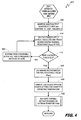
- FIG. 4 is a logical flowchart illustrating a method for thermal management using thermal resistance values to predict optimum power level settings in a PCD 100.
- Method 400 of FIG. 4 starts with a first block 405 in which temperature sensors 157 reading junction temperatures of processing components, such as cores 222, 224, 226, 228, are polled by the monitor module 114.
- the temperature readings taken at block 405 may be compared against a temperature threshold to determine if an operating temperature has exceeded the threshold.
- the temperature readings which represent instantaneous or real-time temperatures ("T INST ") associated with the exemplary processing components, may be provided to PLP module 101.
- T INST instantaneous or real-time temperatures
- the PLP module 101 may receive indications of the active power levels (“P SUPP ”) being supplied to the exemplary processing components and, in combination with the T INST values and the ambient temperature (“T A ") to which the PCD 100 is exposed, calculate and track instantaneous or real-time values representative of a thermal resistance level (“R INST ”) of the processing components.
- P SUPP active power levels
- T A ambient temperature
- R INST thermal resistance level
- the tracking and monitoring of the T INST and P SUPP values, as well as the calculation and tracking of the R INST values may be ongoing in certain embodiments.
- a T INST value meets or exceeds a temperature threshold such as, for example, a temperature threshold associated with a maximum temperature to which a silicon junction of a core may be exposed. If the T INST value does not exceed the threshold, the "no" branch may be followed to block 420 and the power level settings being supplied to the cores by the DVFS module 26 and/or PMIC 180 may be left unmodified or unadjusted. If the T INST value does exceed the threshold, it may be recognized that thermal mitigation measures should be taken and the "yes" branch is followed to block 425.
- a temperature threshold such as, for example, a temperature threshold associated with a maximum temperature to which a silicon junction of a core may be exposed.
- the PLP module 101 may, based on the R INST value determined and tracked at block 410, the T A value and a target operating temperature in place of the T INST , calculate an adjusted power level setting.
- the PLP module 101 may provide the adjusted power level setting to the DVFS module 26 for modification of the voltage and/or frequency settings of the P SUPP based on the adjusted power level setting.
- embodiments of the systems and methods may more efficiently adjust DVFS settings to manage thermal energy generation in a PCD 100.
- certain embodiments may recognize that a T INST value is well below a certain temperature threshold and thereby determine that additional capacity for thermal energy generation is available. In such a scenario, certain embodiments may conduct the actions of blocks 425-435 to adjust power settings of the cores upward, thereby providing increased processing speed and improved QoS.
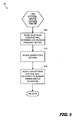
- FIG. 5 is a logical flowchart illustrating sub-method or subroutine 435 for applying dynamic voltage and frequency scaling ("DVFS") thermal management techniques.
- DVFS techniques may be leveraged by a PLP module 101 in the application of thermal management policies that determine optimum power supply levels based on instantaneous thermal resistance values.
- the DVFS throttling techniques may be applied to individual processing components such that an active power supply level is adjusted to an optimum level for management of thermal energy generation.
- DVCS dynamic voltage and current scaling
- a reduction in operating voltage usually results in a proportional savings in power consumed.
- One main issue for DVFS enabled processors 110, 126 is how to control the balance between performance and power savings.
- Block 505 is the first step in the submethod or subroutine 435 for applying DVFS thermal mitigation techniques in a system or method that manages thermal energy generation through predicted power levels based on thermal resistance values.
- the PLP module 101 may determine that a temperature threshold, such as a junction threshold, has been violated based on temperature readings provided by thermal sensors 157A through monitor module 114. Accordingly, the PLP module 101 may then calculate an adjusted power supply level that, given the instantaneous thermal resistance level R INST , may drive the thermal energy generation to an acceptable level. The PLP module 101 may then initiate instructions to the DVFS module 26 to review the current DVFS settings in block 510 and adjust the DVFS settings at block 515 commensurate with the calculated adjusted power supply level.
- a temperature threshold such as a junction threshold
- the DVFS module 26 may issue commands to adjust the current DVFS settings that may include voltage and/or frequency, in order to mitigate thermal loading conditions or, alternatively, allow for increased thermal generation. Adjusting the settings may comprise adjusting or "scaling" the maximum clock frequency allowed in DVFS algorithm. As described above, the DVFS module 26 may be dedicated to a processing component and adjust the power level to the processing component in accordance with the optimum power level provided by the PLP module 101.
- monitor module 114 PLP module 101 and DVFS module 26 have been described in the present disclosure as separate modules with separate functionality, it will be understood that in some embodiments the various modules, or aspects of the various modules, may be combined into a common module for implementing systems and methods for thermal management by power level prediction.
- the functions described may be implemented in hardware, software, firmware, or any combination thereof. If implemented in software, the functions may be stored on or transmitted as one or more instructions or code on a computer-readable medium.
- Computer-readable media include both computer storage media and communication media including any medium that facilitates transfer of a computer program from one place to another.
- a storage media may be any available media that may be accessed by a computer.
- such computer-readable media may comprise RAM, ROM, EEPROM, CD-ROM or other optical disk storage, magnetic disk storage or other magnetic storage devices, or any other medium that may be used to carry or store desired program code in the form of instructions or data structures and that may be accessed by a computer.
- any connection is properly termed a computer-readable medium.
- the software is transmitted from a website, server, or other remote source using a coaxial cable, fiber optic cable, twisted pair, digital subscriber line ("DSL"), or wireless technologies such as infrared, radio, and microwave
- coaxial cable, fiber optic cable, twisted pair, DSL, or wireless technologies such as infrared, radio, and microwave are included in the definition of medium.
- Disk and disc includes compact disc (“CD”), laser disc, optical disc, digital versatile disc (“DVD”), floppy disk and blu-ray disc where disks usually reproduce data magnetically, while discs reproduce data optically with lasers. Combinations of the above should also be included within the scope of computer-readable media.
Landscapes
- Engineering & Computer Science (AREA)
- Theoretical Computer Science (AREA)
- Physics & Mathematics (AREA)
- General Engineering & Computer Science (AREA)
- General Physics & Mathematics (AREA)
- Human Computer Interaction (AREA)
- Computer Hardware Design (AREA)
- Power Sources (AREA)
Claims (15)
- Procédé (400) de gestion d'une génération d'énergie thermique dans un dispositif calculateur portable « PCD » (100), le procédé comprenant :la définition de seuils de température associés à un ou plusieurs composants du PCD (100) ;la surveillance d'un ou plusieurs capteurs de température (157) du PCD (100), dans lequel chaque capteur de température (157) est associé à un des un ou plusieurs composants et génère des signaux qui représentent une température instantanée ;le suivi (410) d'une valeur de résistance thermique instantanée associée à chacun des un ou plusieurs composants, dans lequel la valeur de résistance thermique d'un composant est calculée à partir de la température instantanée du composant, de l'alimentation électrique active du composant et de la température ambiante du PCD (100) ;la détermination (415) qu'un seuil de température associé à au moins l'un des un ou plusieurs composants a été dépassé ; le calcul (430) d'une alimentation électrique ajustée pour le au moins un des un ou plusieurs composants, dans lequel l'alimentation électrique ajustée est calculée à partir d'une température cible du composant, de la température ambiante du PCD (100) et de la valeur de résistance thermique instantanée associée au composant ; etl'application de l'alimentation électrique ajustée au composant.
- Procédé selon la revendication 1, dans lequel au moins l'un des un ou plusieurs capteurs de température (157) est associé à une jonction silicium d'un noyau.
- Procédé selon la revendication 1, dans lequel au moins l'un des un ou plusieurs capteurs de température (157) est associé à un composant de mémoire boitier sur boitier « PoP ».
- Procédé selon la revendication 1, dans lequel la température cible est inférieure à la température instantanée.
- Procédé selon la revendication 1, dans lequel la température cible est supérieure à la température instantanée.
- Procédé selon la revendication 1, dans lequel l'application de l'alimentation électrique ajustée comprend en outre la mise à l'échelle de la tension et/ou de la fréquence de l'alimentation électrique active.
- Procédé selon la revendication 6, dans lequel l'alimentation électrique ajustée est inférieure à l'alimentation électrique active.
- Procédé selon la revendication 6, dans lequel l'alimentation électrique ajustée est supérieure à l'alimentation électrique active.
- Procédé selon la revendication 1, dans lequel le PCD (100) se présente sous la forme d'un téléphone sans fil.
- Procédé selon la revendication 1, dans lequel l'énergie thermique générée par les composants de traitements dans le PCD (100) ne peut pas être gérée avec un composant de ventilation.
- Système informatique pour gérer la génération d'énergie électrique dans un dispositif calculateur portable « PCD » (100), le système comprenant :des moyens pour définir des seuils de température associés à un ou plusieurs composants du PCD (100) ;des moyens pour surveiller un ou plusieurs capteurs de température (157) dans le PCD (100), dans lequel chaque capteur de température (157) est associé à l'un des un ou plusieurs composants et génère des signaux qui représentent une température instantanée ;des moyens pour suivre une valeur de résistance thermique instantanée associée à chacun des un ou plusieurs composants, dans lequel la valeur de résistance thermique d'un composant est calculée à partir de la température instantanée du composant, d'une alimentation électrique active au composant et d'une température ambiante du PCD (100) ;des moyens pour déterminer qu'un seuil de température associé à au moins l'un des un ou plusieurs composants a été dépassé ; des moyens pour calculer une alimentation électrique ajustée pour le au moins un des un ou plusieurs composants, dans lequel l'alimentation électrique ajustée est calculée à partir d'une température cible du composant, de la température ambiante du PCD (100) et de la valeur de résistance thermique instantanée associée au composant ; etdes moyens pour appliquer l'alimentation électrique ajustée au composant.
- Système informatique selon la revendication 11, dans lequel au moins l'un des un ou plusieurs capteurs de température (157) est associé à une jonction silicium d'un noyau.
- Système informatique selon la revendication 11, dans lequel au moins l'un des un ou plusieurs capteurs de température (157) est associé à un composant de mémoire boitier sur boitier « PoP ».
- Système informatique selon la revendication 11, dans lequel la température cible est inférieure à la température instantanée.
- Programme d'ordinateur comprenant des instructions pour mettre en oeuvre un procédé selon l'une quelconque des revendications précédentes 1 à 10.
Applications Claiming Priority (2)
| Application Number | Priority Date | Filing Date | Title |
|---|---|---|---|
| US13/779,153 US9037882B2 (en) | 2013-02-27 | 2013-02-27 | System and method for thermal management in a portable computing device using thermal resistance values to predict optimum power levels |
| PCT/US2014/018774 WO2014134211A1 (fr) | 2013-02-27 | 2014-02-26 | Système et procédé de gestion thermique dans un dispositif informatique portable en utilisant des valeurs de résistance thermique pour prédire des niveaux de puissance optimaux |
Publications (2)
| Publication Number | Publication Date |
|---|---|
| EP2962169A1 EP2962169A1 (fr) | 2016-01-06 |
| EP2962169B1 true EP2962169B1 (fr) | 2016-10-12 |
Family
ID=50342488
Family Applications (1)
| Application Number | Title | Priority Date | Filing Date |
|---|---|---|---|
| EP14711648.7A Not-in-force EP2962169B1 (fr) | 2013-02-27 | 2014-02-26 | Système et procédé de gestion thermique dans un dispositif informatique portable en utilisant des valeurs de résistance thermique pour prédire des niveaux de puissance optimaux |
Country Status (6)
| Country | Link |
|---|---|
| US (2) | US9037882B2 (fr) |
| EP (1) | EP2962169B1 (fr) |
| JP (1) | JP6162262B2 (fr) |
| KR (1) | KR101814264B1 (fr) |
| CN (1) | CN105009021B (fr) |
| WO (1) | WO2014134211A1 (fr) |
Families Citing this family (31)
| Publication number | Priority date | Publication date | Assignee | Title |
|---|---|---|---|---|
| US9037882B2 (en) | 2013-02-27 | 2015-05-19 | Qualcomm Incorporated | System and method for thermal management in a portable computing device using thermal resistance values to predict optimum power levels |
| JP6136596B2 (ja) * | 2013-06-05 | 2017-05-31 | 富士通株式会社 | 監視制御装置、監視制御方法及び監視制御プログラム |
| US9625963B2 (en) | 2014-08-29 | 2017-04-18 | Qualcomm Incorporated | Thermally-constrained voltage and frequency scaling |
| US9903764B2 (en) * | 2014-09-30 | 2018-02-27 | Samsung Electronics Co., Ltd. | Integrated circuit for estimating power of at least one node using temperature and a system including the same |
| US20160117199A1 (en) * | 2014-10-28 | 2016-04-28 | Samsung Electronics Co., Ltd. | Computing system with thermal mechanism and method of operation thereof |
| US9582052B2 (en) * | 2014-10-30 | 2017-02-28 | Qualcomm Incorporated | Thermal mitigation of multi-core processor |
| US9958921B2 (en) | 2015-03-09 | 2018-05-01 | Advanced Micro Devices, Inc. | Power management to change power limits based on device skin temperature |
| US20160266629A1 (en) * | 2015-03-09 | 2016-09-15 | Advanced Micro Devices, Inc. | Changing power limits based on device state |
| US9785209B2 (en) * | 2015-03-31 | 2017-10-10 | Qualcomm Incorporated | Thermal management in a computing device based on workload detection |
| US10215800B2 (en) * | 2015-04-24 | 2019-02-26 | Qualcomm Incorporated | Device specific thermal mitigation |
| US20170083063A1 (en) * | 2015-09-21 | 2017-03-23 | Qualcomm Incorporated | Circuits and methods providing temperature mitigation for computing devices using in-package sensor |
| US10187282B2 (en) * | 2015-10-01 | 2019-01-22 | Qualcomm Incorporated | System and method for modem management based on key performance indicators |
| US9733685B2 (en) | 2015-12-14 | 2017-08-15 | International Business Machines Corporation | Temperature-aware microprocessor voltage management |
| US10168752B2 (en) * | 2016-03-08 | 2019-01-01 | Qualcomm Incorporated | Systems and methods for determining a sustained thermal power envelope comprising multiple heat sources |
| US10496141B2 (en) * | 2016-03-17 | 2019-12-03 | Qualcomm Incorporated | System and method for intelligent thermal management in a system on a chip having a heterogeneous cluster architecture |
| US10248173B2 (en) * | 2016-03-31 | 2019-04-02 | Intel Corporation | Determining thermal margins in a multi-die processor |
| JP2017195494A (ja) * | 2016-04-20 | 2017-10-26 | 富士通株式会社 | ラインカード及びラインカード制御方法 |
| EP3264268A1 (fr) * | 2016-06-29 | 2018-01-03 | Intel Corporation | Algorithme de qos de traitement distribué permettant d'optimiser les performances d'un système sous des contraintes thermiques |
| US20180056428A1 (en) * | 2016-08-31 | 2018-03-01 | Esab Ab | Dynamic Power Limitation |
| CN106656796B (zh) * | 2016-11-11 | 2020-04-24 | 中国人民解放军国防科学技术大学 | 一种基于温度等级的超前阶梯式缓冲区调节方法 |
| KR102643797B1 (ko) * | 2017-01-10 | 2024-03-05 | 삼성전자주식회사 | 동적 발열 관리 방법 |
| JP6872440B2 (ja) * | 2017-06-30 | 2021-05-19 | ルネサスエレクトロニクス株式会社 | 半導体装置および半導体装置の制御方法 |
| WO2019067329A1 (fr) * | 2017-09-28 | 2019-04-04 | Qualcomm Incorporated | Gestion thermique de modem |
| US10409359B2 (en) * | 2018-01-17 | 2019-09-10 | Qualcomm Incorporated | Dynamic bin ordering for load synchronization |
| CN109710003A (zh) * | 2018-12-26 | 2019-05-03 | 联想(北京)有限公司 | 温度控制方法及系统 |
| KR20210032213A (ko) | 2019-09-16 | 2021-03-24 | 삼성전자주식회사 | 전력 스텝에 기초한 동적 다이내믹 전압 주파주 스케일링(dvfs) 수행 방법 |
| US11892893B2 (en) | 2019-10-01 | 2024-02-06 | Microsoft Technology Licensing, Llc | Systems and methods for thermal system management |
| WO2021066829A1 (fr) * | 2019-10-03 | 2021-04-08 | Hewlett-Packard Development Company, L.P. | Modification de paramètres de surfréquençage |
| US11460423B2 (en) * | 2020-02-25 | 2022-10-04 | Dell Products L.P. | System and method to create an air flow map and detect air recirculation in an information handling system |
| KR20220059243A (ko) * | 2020-11-02 | 2022-05-10 | 삼성전자주식회사 | 전력 측정에 기초한 온도 검출 및 열 관리를 위한 방법 및 장치 |
| CN113157438A (zh) * | 2021-03-10 | 2021-07-23 | 电子科技大学 | 一种高能效比多核微处理器的动态热管理方法 |
Family Cites Families (17)
| Publication number | Priority date | Publication date | Assignee | Title |
|---|---|---|---|---|
| US5805403A (en) | 1996-03-28 | 1998-09-08 | 3Com Ltd. | Integrated circuit temperature monitoring and protection system |
| US7111178B2 (en) | 2001-09-28 | 2006-09-19 | Intel Corporation | Method and apparatus for adjusting the voltage and frequency to minimize power dissipation in a multiprocessor system |
| US7076672B2 (en) | 2002-10-14 | 2006-07-11 | Intel Corporation | Method and apparatus for performance effective power throttling |
| US7275012B2 (en) * | 2002-12-30 | 2007-09-25 | Intel Corporation | Automated method and apparatus for processor thermal validation |
| JP3811166B2 (ja) * | 2004-05-31 | 2006-08-16 | 株式会社東芝 | 電子機器 |
| US7461272B2 (en) * | 2004-12-21 | 2008-12-02 | Intel Corporation | Device, system and method of thermal control |
| US8374730B2 (en) * | 2005-08-25 | 2013-02-12 | Apple Inc. | Methods and apparatuses for dynamic thermal control |
| US8762097B2 (en) | 2006-08-04 | 2014-06-24 | Apple Inc. | Method and apparatus for a thermal control system based on virtual temperature sensor |
| US7887235B2 (en) | 2006-08-30 | 2011-02-15 | Freescale Semiconductor, Inc. | Multiple sensor thermal management for electronic devices |
| US20080234953A1 (en) | 2007-03-22 | 2008-09-25 | Ignowski James S | Power estimation for a semiconductor device |
| US8620235B2 (en) * | 2008-05-23 | 2013-12-31 | Qualcomm Incorporated | Thermal management for data modules |
| US8182139B2 (en) | 2008-05-30 | 2012-05-22 | Apple Inc. | Calibration of temperature sensing circuitry in an electronic device |
| US8392340B2 (en) * | 2009-03-13 | 2013-03-05 | Apple Inc. | Method and apparatus for detecting conditions of a peripheral device including motion, and determining/predicting temperature(S) wherein at least one temperature is weighted based on detected conditions |
| US8996330B2 (en) | 2011-01-06 | 2015-03-31 | Qualcomm Incorporated | Method and system for managing thermal policies of a portable computing device |
| JP5296136B2 (ja) * | 2011-04-11 | 2013-09-25 | 株式会社ソニー・コンピュータエンタテインメント | 電子機器、その制御方法、及び半導体集積回路 |
| US9250664B2 (en) * | 2012-02-24 | 2016-02-02 | Dell Products L.P. | IHS component cooling system |
| US9037882B2 (en) | 2013-02-27 | 2015-05-19 | Qualcomm Incorporated | System and method for thermal management in a portable computing device using thermal resistance values to predict optimum power levels |
-
2013
- 2013-02-27 US US13/779,153 patent/US9037882B2/en active Active
-
2014
- 2014-02-26 JP JP2015559308A patent/JP6162262B2/ja not_active Expired - Fee Related
- 2014-02-26 WO PCT/US2014/018774 patent/WO2014134211A1/fr active Application Filing
- 2014-02-26 KR KR1020157025751A patent/KR101814264B1/ko active IP Right Grant
- 2014-02-26 CN CN201480010310.XA patent/CN105009021B/zh not_active Expired - Fee Related
- 2014-02-26 EP EP14711648.7A patent/EP2962169B1/fr not_active Not-in-force
-
2015
- 2015-04-17 US US14/690,330 patent/US9465423B2/en active Active
Also Published As
| Publication number | Publication date |
|---|---|
| KR101814264B1 (ko) | 2018-01-02 |
| KR20150121707A (ko) | 2015-10-29 |
| EP2962169A1 (fr) | 2016-01-06 |
| CN105009021B (zh) | 2018-07-03 |
| US9037882B2 (en) | 2015-05-19 |
| JP2016510917A (ja) | 2016-04-11 |
| CN105009021A (zh) | 2015-10-28 |
| JP6162262B2 (ja) | 2017-07-12 |
| US9465423B2 (en) | 2016-10-11 |
| WO2014134211A1 (fr) | 2014-09-04 |
| US20140245032A1 (en) | 2014-08-28 |
| US20150220125A1 (en) | 2015-08-06 |
Similar Documents
| Publication | Publication Date | Title |
|---|---|---|
| EP2962169B1 (fr) | Système et procédé de gestion thermique dans un dispositif informatique portable en utilisant des valeurs de résistance thermique pour prédire des niveaux de puissance optimaux | |
| US9360907B2 (en) | System and method for adaptive thermal management in a portable computing device | |
| EP2929409B1 (fr) | Système et procédé pour estimer la température ambiante à partir d'un dispositif informatique portable | |
| US9703336B2 (en) | System and method for thermal management in a multi-functional portable computing device | |
| US10037258B2 (en) | System and method for intelligent thermal management using dynamic performance floors in a portable computing device | |
| US8942857B2 (en) | Method and system for thermal load management in a portable computing device | |
| US20130090888A1 (en) | System and method for proximity based thermal management of mobile device | |
| EP3430496B1 (fr) | Système et procédé de gestion thermique intelligente dans un système sur puce ayant une architecture de grappe hétérogène | |
| EP2766788B1 (fr) | Système et procédé permettant de déterminer une politique de gestion thermique à partir d'une mesure de courant de fuite | |
| US20160070327A1 (en) | System and method for peak current management to a system on a chip | |
| WO2015010044A1 (fr) | Système et procédé pour optimiser un état inactif dans un système multiprocesseur sur une puce | |
| WO2015077671A1 (fr) | Système et procédé pour une gestion thermique d'apprentissage multi-corrélatif d'un système sur une puce dans un dispositif informatique portable | |
| WO2014130339A1 (fr) | Système et procédé de sélection pilotée par la température des modes de tension dans un dispositif informatique portable |
Legal Events
| Date | Code | Title | Description |
|---|---|---|---|
| PUAI | Public reference made under article 153(3) epc to a published international application that has entered the european phase |
Free format text: ORIGINAL CODE: 0009012 |
|
| 17P | Request for examination filed |
Effective date: 20150918 |
|
| AK | Designated contracting states |
Kind code of ref document: A1 Designated state(s): AL AT BE BG CH CY CZ DE DK EE ES FI FR GB GR HR HU IE IS IT LI LT LU LV MC MK MT NL NO PL PT RO RS SE SI SK SM TR |
|
| AX | Request for extension of the european patent |
Extension state: BA ME |
|
| GRAP | Despatch of communication of intention to grant a patent |
Free format text: ORIGINAL CODE: EPIDOSNIGR1 |
|
| DAX | Request for extension of the european patent (deleted) | ||
| INTG | Intention to grant announced |
Effective date: 20160510 |
|
| GRAS | Grant fee paid |
Free format text: ORIGINAL CODE: EPIDOSNIGR3 |
|
| GRAA | (expected) grant |
Free format text: ORIGINAL CODE: 0009210 |
|
| AK | Designated contracting states |
Kind code of ref document: B1 Designated state(s): AL AT BE BG CH CY CZ DE DK EE ES FI FR GB GR HR HU IE IS IT LI LT LU LV MC MK MT NL NO PL PT RO RS SE SI SK SM TR |
|
| REG | Reference to a national code |
Ref country code: GB Ref legal event code: FG4D |
|
| REG | Reference to a national code |
Ref country code: CH Ref legal event code: EP |
|
| REG | Reference to a national code |
Ref country code: AT Ref legal event code: REF Ref document number: 837063 Country of ref document: AT Kind code of ref document: T Effective date: 20161015 |
|
| REG | Reference to a national code |
Ref country code: IE Ref legal event code: FG4D |
|
| REG | Reference to a national code |
Ref country code: DE Ref legal event code: R096 Ref document number: 602014004239 Country of ref document: DE |
|
| REG | Reference to a national code |
Ref country code: LT Ref legal event code: MG4D |
|
| REG | Reference to a national code |
Ref country code: FR Ref legal event code: PLFP Year of fee payment: 4 |
|
| REG | Reference to a national code |
Ref country code: NL Ref legal event code: MP Effective date: 20161012 |
|
| PG25 | Lapsed in a contracting state [announced via postgrant information from national office to epo] |
Ref country code: LV Free format text: LAPSE BECAUSE OF FAILURE TO SUBMIT A TRANSLATION OF THE DESCRIPTION OR TO PAY THE FEE WITHIN THE PRESCRIBED TIME-LIMIT Effective date: 20161012 |
|
| REG | Reference to a national code |
Ref country code: AT Ref legal event code: MK05 Ref document number: 837063 Country of ref document: AT Kind code of ref document: T Effective date: 20161012 |
|
| PG25 | Lapsed in a contracting state [announced via postgrant information from national office to epo] |
Ref country code: NO Free format text: LAPSE BECAUSE OF FAILURE TO SUBMIT A TRANSLATION OF THE DESCRIPTION OR TO PAY THE FEE WITHIN THE PRESCRIBED TIME-LIMIT Effective date: 20170112 Ref country code: GR Free format text: LAPSE BECAUSE OF FAILURE TO SUBMIT A TRANSLATION OF THE DESCRIPTION OR TO PAY THE FEE WITHIN THE PRESCRIBED TIME-LIMIT Effective date: 20170113 Ref country code: SE Free format text: LAPSE BECAUSE OF FAILURE TO SUBMIT A TRANSLATION OF THE DESCRIPTION OR TO PAY THE FEE WITHIN THE PRESCRIBED TIME-LIMIT Effective date: 20161012 Ref country code: LT Free format text: LAPSE BECAUSE OF FAILURE TO SUBMIT A TRANSLATION OF THE DESCRIPTION OR TO PAY THE FEE WITHIN THE PRESCRIBED TIME-LIMIT Effective date: 20161012 |
|
| PG25 | Lapsed in a contracting state [announced via postgrant information from national office to epo] |
Ref country code: RS Free format text: LAPSE BECAUSE OF FAILURE TO SUBMIT A TRANSLATION OF THE DESCRIPTION OR TO PAY THE FEE WITHIN THE PRESCRIBED TIME-LIMIT Effective date: 20161012 Ref country code: PL Free format text: LAPSE BECAUSE OF FAILURE TO SUBMIT A TRANSLATION OF THE DESCRIPTION OR TO PAY THE FEE WITHIN THE PRESCRIBED TIME-LIMIT Effective date: 20161012 Ref country code: HR Free format text: LAPSE BECAUSE OF FAILURE TO SUBMIT A TRANSLATION OF THE DESCRIPTION OR TO PAY THE FEE WITHIN THE PRESCRIBED TIME-LIMIT Effective date: 20161012 Ref country code: NL Free format text: LAPSE BECAUSE OF FAILURE TO SUBMIT A TRANSLATION OF THE DESCRIPTION OR TO PAY THE FEE WITHIN THE PRESCRIBED TIME-LIMIT Effective date: 20161012 Ref country code: FI Free format text: LAPSE BECAUSE OF FAILURE TO SUBMIT A TRANSLATION OF THE DESCRIPTION OR TO PAY THE FEE WITHIN THE PRESCRIBED TIME-LIMIT Effective date: 20161012 Ref country code: AT Free format text: LAPSE BECAUSE OF FAILURE TO SUBMIT A TRANSLATION OF THE DESCRIPTION OR TO PAY THE FEE WITHIN THE PRESCRIBED TIME-LIMIT Effective date: 20161012 Ref country code: IS Free format text: LAPSE BECAUSE OF FAILURE TO SUBMIT A TRANSLATION OF THE DESCRIPTION OR TO PAY THE FEE WITHIN THE PRESCRIBED TIME-LIMIT Effective date: 20170212 Ref country code: BE Free format text: LAPSE BECAUSE OF FAILURE TO SUBMIT A TRANSLATION OF THE DESCRIPTION OR TO PAY THE FEE WITHIN THE PRESCRIBED TIME-LIMIT Effective date: 20161012 Ref country code: PT Free format text: LAPSE BECAUSE OF FAILURE TO SUBMIT A TRANSLATION OF THE DESCRIPTION OR TO PAY THE FEE WITHIN THE PRESCRIBED TIME-LIMIT Effective date: 20170213 Ref country code: ES Free format text: LAPSE BECAUSE OF FAILURE TO SUBMIT A TRANSLATION OF THE DESCRIPTION OR TO PAY THE FEE WITHIN THE PRESCRIBED TIME-LIMIT Effective date: 20161012 |
|
| REG | Reference to a national code |
Ref country code: DE Ref legal event code: R097 Ref document number: 602014004239 Country of ref document: DE |
|
| PG25 | Lapsed in a contracting state [announced via postgrant information from national office to epo] |
Ref country code: EE Free format text: LAPSE BECAUSE OF FAILURE TO SUBMIT A TRANSLATION OF THE DESCRIPTION OR TO PAY THE FEE WITHIN THE PRESCRIBED TIME-LIMIT Effective date: 20161012 Ref country code: DK Free format text: LAPSE BECAUSE OF FAILURE TO SUBMIT A TRANSLATION OF THE DESCRIPTION OR TO PAY THE FEE WITHIN THE PRESCRIBED TIME-LIMIT Effective date: 20161012 Ref country code: SK Free format text: LAPSE BECAUSE OF FAILURE TO SUBMIT A TRANSLATION OF THE DESCRIPTION OR TO PAY THE FEE WITHIN THE PRESCRIBED TIME-LIMIT Effective date: 20161012 Ref country code: CZ Free format text: LAPSE BECAUSE OF FAILURE TO SUBMIT A TRANSLATION OF THE DESCRIPTION OR TO PAY THE FEE WITHIN THE PRESCRIBED TIME-LIMIT Effective date: 20161012 Ref country code: RO Free format text: LAPSE BECAUSE OF FAILURE TO SUBMIT A TRANSLATION OF THE DESCRIPTION OR TO PAY THE FEE WITHIN THE PRESCRIBED TIME-LIMIT Effective date: 20161012 |
|
| PLBE | No opposition filed within time limit |
Free format text: ORIGINAL CODE: 0009261 |
|
| STAA | Information on the status of an ep patent application or granted ep patent |
Free format text: STATUS: NO OPPOSITION FILED WITHIN TIME LIMIT |
|
| PG25 | Lapsed in a contracting state [announced via postgrant information from national office to epo] |
Ref country code: SM Free format text: LAPSE BECAUSE OF FAILURE TO SUBMIT A TRANSLATION OF THE DESCRIPTION OR TO PAY THE FEE WITHIN THE PRESCRIBED TIME-LIMIT Effective date: 20161012 Ref country code: IT Free format text: LAPSE BECAUSE OF FAILURE TO SUBMIT A TRANSLATION OF THE DESCRIPTION OR TO PAY THE FEE WITHIN THE PRESCRIBED TIME-LIMIT Effective date: 20161012 Ref country code: BG Free format text: LAPSE BECAUSE OF FAILURE TO SUBMIT A TRANSLATION OF THE DESCRIPTION OR TO PAY THE FEE WITHIN THE PRESCRIBED TIME-LIMIT Effective date: 20170112 |
|
| 26N | No opposition filed |
Effective date: 20170713 |
|
| PG25 | Lapsed in a contracting state [announced via postgrant information from national office to epo] |
Ref country code: MC Free format text: LAPSE BECAUSE OF FAILURE TO SUBMIT A TRANSLATION OF THE DESCRIPTION OR TO PAY THE FEE WITHIN THE PRESCRIBED TIME-LIMIT Effective date: 20161012 |
|
| REG | Reference to a national code |
Ref country code: CH Ref legal event code: PL |
|
| PG25 | Lapsed in a contracting state [announced via postgrant information from national office to epo] |
Ref country code: LI Free format text: LAPSE BECAUSE OF NON-PAYMENT OF DUE FEES Effective date: 20170228 Ref country code: CH Free format text: LAPSE BECAUSE OF NON-PAYMENT OF DUE FEES Effective date: 20170228 |
|
| REG | Reference to a national code |
Ref country code: IE Ref legal event code: MM4A |
|
| PG25 | Lapsed in a contracting state [announced via postgrant information from national office to epo] |
Ref country code: SI Free format text: LAPSE BECAUSE OF FAILURE TO SUBMIT A TRANSLATION OF THE DESCRIPTION OR TO PAY THE FEE WITHIN THE PRESCRIBED TIME-LIMIT Effective date: 20161012 |
|
| PG25 | Lapsed in a contracting state [announced via postgrant information from national office to epo] |
Ref country code: LU Free format text: LAPSE BECAUSE OF NON-PAYMENT OF DUE FEES Effective date: 20170226 |
|
| REG | Reference to a national code |
Ref country code: FR Ref legal event code: PLFP Year of fee payment: 5 |
|
| PG25 | Lapsed in a contracting state [announced via postgrant information from national office to epo] |
Ref country code: IE Free format text: LAPSE BECAUSE OF NON-PAYMENT OF DUE FEES Effective date: 20170226 |
|
| PGFP | Annual fee paid to national office [announced via postgrant information from national office to epo] |
Ref country code: GB Payment date: 20180125 Year of fee payment: 5 |
|
| PG25 | Lapsed in a contracting state [announced via postgrant information from national office to epo] |
Ref country code: MT Free format text: LAPSE BECAUSE OF NON-PAYMENT OF DUE FEES Effective date: 20170226 |
|
| PG25 | Lapsed in a contracting state [announced via postgrant information from national office to epo] |
Ref country code: HU Free format text: LAPSE BECAUSE OF FAILURE TO SUBMIT A TRANSLATION OF THE DESCRIPTION OR TO PAY THE FEE WITHIN THE PRESCRIBED TIME-LIMIT; INVALID AB INITIO Effective date: 20140226 |
|
| GBPC | Gb: european patent ceased through non-payment of renewal fee |
Effective date: 20190226 |
|
| PG25 | Lapsed in a contracting state [announced via postgrant information from national office to epo] |
Ref country code: CY Free format text: LAPSE BECAUSE OF FAILURE TO SUBMIT A TRANSLATION OF THE DESCRIPTION OR TO PAY THE FEE WITHIN THE PRESCRIBED TIME-LIMIT Effective date: 20161012 |
|
| PG25 | Lapsed in a contracting state [announced via postgrant information from national office to epo] |
Ref country code: MK Free format text: LAPSE BECAUSE OF FAILURE TO SUBMIT A TRANSLATION OF THE DESCRIPTION OR TO PAY THE FEE WITHIN THE PRESCRIBED TIME-LIMIT Effective date: 20161012 |
|
| PG25 | Lapsed in a contracting state [announced via postgrant information from national office to epo] |
Ref country code: GB Free format text: LAPSE BECAUSE OF NON-PAYMENT OF DUE FEES Effective date: 20190226 |
|
| PG25 | Lapsed in a contracting state [announced via postgrant information from national office to epo] |
Ref country code: TR Free format text: LAPSE BECAUSE OF FAILURE TO SUBMIT A TRANSLATION OF THE DESCRIPTION OR TO PAY THE FEE WITHIN THE PRESCRIBED TIME-LIMIT Effective date: 20161012 |
|
| PGFP | Annual fee paid to national office [announced via postgrant information from national office to epo] |
Ref country code: DE Payment date: 20200115 Year of fee payment: 7 |
|
| PGFP | Annual fee paid to national office [announced via postgrant information from national office to epo] |
Ref country code: FR Payment date: 20200124 Year of fee payment: 7 |
|
| PG25 | Lapsed in a contracting state [announced via postgrant information from national office to epo] |
Ref country code: AL Free format text: LAPSE BECAUSE OF FAILURE TO SUBMIT A TRANSLATION OF THE DESCRIPTION OR TO PAY THE FEE WITHIN THE PRESCRIBED TIME-LIMIT Effective date: 20161012 |
|
| REG | Reference to a national code |
Ref country code: DE Ref legal event code: R119 Ref document number: 602014004239 Country of ref document: DE |
|
| PG25 | Lapsed in a contracting state [announced via postgrant information from national office to epo] |
Ref country code: DE Free format text: LAPSE BECAUSE OF NON-PAYMENT OF DUE FEES Effective date: 20210901 Ref country code: FR Free format text: LAPSE BECAUSE OF NON-PAYMENT OF DUE FEES Effective date: 20210228 |