EP2950339A1 - Semiconductor device - Google Patents
Semiconductor device Download PDFInfo
- Publication number
- EP2950339A1 EP2950339A1 EP15165397.9A EP15165397A EP2950339A1 EP 2950339 A1 EP2950339 A1 EP 2950339A1 EP 15165397 A EP15165397 A EP 15165397A EP 2950339 A1 EP2950339 A1 EP 2950339A1
- Authority
- EP
- European Patent Office
- Prior art keywords
- layer
- embedded
- semiconductor device
- base substrate
- embedded layer
- Prior art date
- Legal status (The legal status is an assumption and is not a legal conclusion. Google has not performed a legal analysis and makes no representation as to the accuracy of the status listed.)
- Withdrawn
Links
Images




Classifications
-
- H—ELECTRICITY
- H10—SEMICONDUCTOR DEVICES; ELECTRIC SOLID-STATE DEVICES NOT OTHERWISE PROVIDED FOR
- H10D—INORGANIC ELECTRIC SEMICONDUCTOR DEVICES
- H10D12/00—Bipolar devices controlled by the field effect, e.g. insulated-gate bipolar transistors [IGBT]
- H10D12/411—Insulated-gate bipolar transistors [IGBT]
- H10D12/441—Vertical IGBTs
- H10D12/461—Vertical IGBTs having non-planar surfaces, e.g. having trenches, recesses or pillars in the surfaces of the emitter, base or collector regions
- H10D12/481—Vertical IGBTs having non-planar surfaces, e.g. having trenches, recesses or pillars in the surfaces of the emitter, base or collector regions having gate structures on slanted surfaces, on vertical surfaces, or in grooves, e.g. trench gate IGBTs
-
- H—ELECTRICITY
- H10—SEMICONDUCTOR DEVICES; ELECTRIC SOLID-STATE DEVICES NOT OTHERWISE PROVIDED FOR
- H10D—INORGANIC ELECTRIC SEMICONDUCTOR DEVICES
- H10D62/00—Semiconductor bodies, or regions thereof, of devices having potential barriers
- H10D62/10—Shapes, relative sizes or dispositions of the regions of the semiconductor bodies; Shapes of the semiconductor bodies
- H10D62/17—Semiconductor regions connected to electrodes not carrying current to be rectified, amplified or switched, e.g. channel regions
- H10D62/393—Body regions of DMOS transistors or IGBTs
-
- H—ELECTRICITY
- H10—SEMICONDUCTOR DEVICES; ELECTRIC SOLID-STATE DEVICES NOT OTHERWISE PROVIDED FOR
- H10D—INORGANIC ELECTRIC SEMICONDUCTOR DEVICES
- H10D84/00—Integrated devices formed in or on semiconductor substrates that comprise only semiconducting layers, e.g. on Si wafers or on GaAs-on-Si wafers
- H10D84/01—Manufacture or treatment
- H10D84/0123—Integrating together multiple components covered by H10D12/00 or H10D30/00, e.g. integrating multiple IGBTs
- H10D84/0126—Integrating together multiple components covered by H10D12/00 or H10D30/00, e.g. integrating multiple IGBTs the components including insulated gates, e.g. IGFETs
- H10D84/0165—Integrating together multiple components covered by H10D12/00 or H10D30/00, e.g. integrating multiple IGBTs the components including insulated gates, e.g. IGFETs the components including complementary IGFETs, e.g. CMOS devices
- H10D84/0191—Manufacturing their doped wells
-
- H—ELECTRICITY
- H10—SEMICONDUCTOR DEVICES; ELECTRIC SOLID-STATE DEVICES NOT OTHERWISE PROVIDED FOR
- H10D—INORGANIC ELECTRIC SEMICONDUCTOR DEVICES
- H10D84/00—Integrated devices formed in or on semiconductor substrates that comprise only semiconducting layers, e.g. on Si wafers or on GaAs-on-Si wafers
- H10D84/01—Manufacture or treatment
- H10D84/02—Manufacture or treatment characterised by using material-based technologies
- H10D84/03—Manufacture or treatment characterised by using material-based technologies using Group IV technology, e.g. silicon technology or silicon-carbide [SiC] technology
- H10D84/038—Manufacture or treatment characterised by using material-based technologies using Group IV technology, e.g. silicon technology or silicon-carbide [SiC] technology using silicon technology, e.g. SiGe
-
- H—ELECTRICITY
- H10—SEMICONDUCTOR DEVICES; ELECTRIC SOLID-STATE DEVICES NOT OTHERWISE PROVIDED FOR
- H10D—INORGANIC ELECTRIC SEMICONDUCTOR DEVICES
- H10D84/00—Integrated devices formed in or on semiconductor substrates that comprise only semiconducting layers, e.g. on Si wafers or on GaAs-on-Si wafers
- H10D84/80—Integrated devices formed in or on semiconductor substrates that comprise only semiconducting layers, e.g. on Si wafers or on GaAs-on-Si wafers characterised by the integration of at least one component covered by groups H10D12/00 or H10D30/00, e.g. integration of IGFETs
- H10D84/82—Integrated devices formed in or on semiconductor substrates that comprise only semiconducting layers, e.g. on Si wafers or on GaAs-on-Si wafers characterised by the integration of at least one component covered by groups H10D12/00 or H10D30/00, e.g. integration of IGFETs of only field-effect components
- H10D84/83—Integrated devices formed in or on semiconductor substrates that comprise only semiconducting layers, e.g. on Si wafers or on GaAs-on-Si wafers characterised by the integration of at least one component covered by groups H10D12/00 or H10D30/00, e.g. integration of IGFETs of only field-effect components of only insulated-gate FETs [IGFET]
- H10D84/8314—Integrated devices formed in or on semiconductor substrates that comprise only semiconducting layers, e.g. on Si wafers or on GaAs-on-Si wafers characterised by the integration of at least one component covered by groups H10D12/00 or H10D30/00, e.g. integration of IGFETs of only field-effect components of only insulated-gate FETs [IGFET] the IGFETs characterised by having gate insulating layers with different properties
-
- H—ELECTRICITY
- H10—SEMICONDUCTOR DEVICES; ELECTRIC SOLID-STATE DEVICES NOT OTHERWISE PROVIDED FOR
- H10D—INORGANIC ELECTRIC SEMICONDUCTOR DEVICES
- H10D84/00—Integrated devices formed in or on semiconductor substrates that comprise only semiconducting layers, e.g. on Si wafers or on GaAs-on-Si wafers
- H10D84/80—Integrated devices formed in or on semiconductor substrates that comprise only semiconducting layers, e.g. on Si wafers or on GaAs-on-Si wafers characterised by the integration of at least one component covered by groups H10D12/00 or H10D30/00, e.g. integration of IGFETs
- H10D84/82—Integrated devices formed in or on semiconductor substrates that comprise only semiconducting layers, e.g. on Si wafers or on GaAs-on-Si wafers characterised by the integration of at least one component covered by groups H10D12/00 or H10D30/00, e.g. integration of IGFETs of only field-effect components
- H10D84/83—Integrated devices formed in or on semiconductor substrates that comprise only semiconducting layers, e.g. on Si wafers or on GaAs-on-Si wafers characterised by the integration of at least one component covered by groups H10D12/00 or H10D30/00, e.g. integration of IGFETs of only field-effect components of only insulated-gate FETs [IGFET]
- H10D84/85—Complementary IGFETs, e.g. CMOS
- H10D84/856—Complementary IGFETs, e.g. CMOS the complementary IGFETs having different architectures than each other, e.g. high-voltage and low-voltage CMOS
Definitions
- the present invention relates to a semiconductor device and is, for example, a technology applicable to a semiconductor device having a diffusion layer embedded into a substrate.
- a diffusion layer is embedded into a substrate and a transistor is formed over the diffusion layer.
- a substance formed by epitaxially growing a semiconductor layer over a semiconductor substrate acting as a base is used as the substrate for example.
- the diffusion layer is: formed by an ion implantation method after the semiconductor layer is formed in some cases; or formed when the semiconductor layer is epitaxially grown in other cases.
- Japanese Unexamined Patent Application Publication No. Sho 62 (1987)-40719 describes that p-type impurities are diffused over the surface of a p-type substrate acting as a base by a thermal diffusion method and successively an epitaxial layer is grown over the substrate.
- Japanese Unexamined Patent Application Publication No. 2002-176177 describes that a semiconductor substrate is formed by forming an n-type epitaxial layer over the surface of a p-type substrate acting as a base and a trench gate type IGBT is formed by using the semiconductor substrate.
- the epitaxial layer has a configuration formed by stacking a low-concentration n-type layer over a high-concentration n-type layer.
- a first electrically conductive type semiconductor layer is formed over a first electrically conductive type base substrate.
- the impurity concentration of the semiconductor layer is lower than that of the base substrate.
- a second electrically conductive type first embedded layer and a second electrically conductive type second embedded layer are formed in the semiconductor layer.
- the second embedded layer is deeper than the first embedded layer, is kept away from the first embedded layer, and has an impurity concentration lower than the first embedded layer.
- a transistor is further formed in the semiconductor layer.
- the embodiment it is possible to inhibit: impurities from diffusing from the substrate to the semiconductor layer; and the withstand voltage of the transistor from deteriorating.
- Fig. 1 is a sectional view showing the configuration of a semiconductor device SD according to First Embodiment.
- the semiconductor device SD according to the present embodiment is formed by using a substrate SUB.
- the substrate SUB is formed by growing an epitaxial layer EPI (semiconductor layer) comprising a semiconductor (for example silicon) over a base substrate BSUB comprising a bulk semiconductor (for example monocrystal silicon).
- EPI semiconductor layer
- Both the base substrate BSUB and the epitaxial layer EPI are an identical electrically conductive type (first electrically conductive type: for example P-type).
- the impurity concentration of the base substrate BSUB is higher than that of the epitaxial layer EPI.
- a first embedded layer BINPL1 that is an electrically conductive type (second electrically conductive type: for example n-type) different from the epitaxial layer EPI is formed in the epitaxial layer EPI.
- the first embedded layer BINPL1 is kept away from the base substrate BSUB.
- the first embedded layer BINPL1 either may be formed when the epitaxial layer EPI is grown epitaxially; or may be formed by an ion implantation method after the epitaxial layer EPI is formed. In the former case, the first embedded layer BINPL1 is formed over the whole surface of the substrate SUB.
- a second embedded layer BINPL2 is formed in the epitaxial layer EPI.
- the second embedded layer BINPL2 is a second electrically conductive type impurity layer, is deeper than the first embedded layer BINPL1, and is kept away from the first embedded layer BINPL1.
- the impurity concentration of the second embedded layer BINPL2 is lower than that of the first embedded layer BINPL1.
- the second embedded layer BINPL2 is formed in order to inhibit: the impurities of the base substrate BSUB from diffusing in the epitaxial layer EPI; and the first electrically conductive type impurity concentration in the lower layer of the epitaxial layer EPI from increasing.
- transistors TR2 and TR3 constituting a logic circuit and a transistor TR1 for electric power control are formed in the epitaxial layer EPI. At least the transistor TR1 overlaps with the first embedded layer BINPL1 in a planar view.
- first electrically conductive type is a p-type and the second electrically conductive type is an n-type. It is also possible however that the first electrically conductive type is an n-type and the second electrically conductive type is a p-type.
- the transistor TR2 is an n-type low withstand voltage transistor and has a gate electrode GE2, a source SOU2, and a drain DRN2.
- the transistor TR3 is a p-type low withstand voltage transistor and has a gate electrode GE3, a source SOU3, and a drain DRN3.
- the transistors TR2 and TR3 include a CMOS transistor. Meanwhile, a gate insulating film (not shown in the figure) is formed under the gate electrodes GE2 and GE3.
- the transistor TR1 is a horizontal transistor for electric power control and has a withstand voltage higher than the transistors TR2 and TR3.
- the transistor TR1 has a gate electrode GE1, a source SOU1, and a drain DRN1.
- the distance between the drain DRN1 and the gate electrode GE1 is larger than the distance between the source SOU1 and the gate electrode GE1.
- the withstand voltage between the drain DRN1 and the gate electrode GE1 is higher.
- a gate insulating film (not shown in the figure) is formed under the gate electrode GE1.
- the gate insulating film is thicker than the gate insulating film of the transistors TR2 and TR3.
- an element isolation insulating film formed by an STI method or a LOCOS method is formed between the drain DRN1 and the gate electrode GE1.
- the drain DRN1 has an n-type well WL12 and an n-type high concentration region HINPL13 formed over the surface layer of the n-type well WL12.
- the high concentration region HINPL13 is coupled to a contact CON3.
- an n - -type offset region NOF11 is formed around the n-type well WL12.
- the n-type well WL12 is formed in the surface layer of the offset region NOF11.
- the source SOU1 has an n-type high concentration region HINPL12.
- the high concentration region HINPL12 is formed in the surface layer of a p-type well WL21. Although it is not shown in the figure, a p-type high concentration region is formed at a part of the p-type well WL21 located adjacent to the high concentration region HINPL12. Then a contact CON2 is coupled to the p-type high concentration region and the high concentration region HINPL12.
- the insulating film HMSK1 is a silicon nitride film for example and the interlayer insulating film INSL1 is a silicon oxide film for example.
- Contacts CON2, CON3, CON4, CON5, CON6, and CON7 are embedded into the insulating film HMSK1 and the interlayer insulating film INSL1.
- the contact CON2 is coupled to the source SOU1 of the transistor TR1 and the contact CON3 is coupled to the drain DRN1 of the transistor TR1.
- the contact CON4 is coupled to the source SOU2 of the transistor TR2 and the contact CON5 is coupled to the drain DRN2 of the transistor TR2.
- the contact CON6 is coupled to the source SOU3 of the transistor TR3 and the contact CON7 is coupled to the drain DRN3 of the transistor TR3. Meanwhile, although they are not shown in the figure, a contact coupled to the gate electrode GE1, a contact coupled to the gate electrode GE2, a contact coupled to the gate electrode GE3, and a contact coupled to a deep well DWL (described later) are also embedded into the insulating film HMSK1 and the interlayer insulating film INSL1.
- Wires INC2, INC3, INC4, INC5, INC6, and INC7 are formed over the interlayer insulating film INSL1.
- the wires INC2, INC3, INC4, INC5, INC6, and INC7 comprise a metal such as aluminum for example and are coupled to the contacts CON2, CON3, CON4, CON5, CON6, and CON7 respectively.
- wires (not shown in the figure) coupled to the respective gate electrodes and a wire (not shown in the figure) coupled to the deep well DWL are also formed over the interlayer insulating film INSL1.
- the transistor TR1 is formed in a first element region EL1 and the transistors TR2 and TR3 are formed in a second element region EL2. More specifically, the single transistor TR1 is formed in the first element region EL1. In contrast, the plural transistors TR2 and TR3 are formed in the second element region EL2. Meanwhile, in Fig. 1 , only a pair of the transistors TR2 and TR3 are shown in the second element region EL2 for the simplification of the figure. Then the first element region EL1 and the second element region EL2 are surrounded by element isolation trenches SDTR respectively.
- the element isolation trenches SDTR pass through the first embedded layer BINPL1 but do not reach the base substrate BSUB. Further in the example shown in the figure, the bottom parts of the element isolation trenches SDTR do not reach even the second embedded layer BINPL2. In other words, the element isolation trenches SDTR are formed so as to be shallower than the second embedded layer BINPL2.
- an embedded insulating film BINSL is embedded into the element isolation trenches SDTR.
- the embedded insulating film BINSL is a part of the interlayer insulating film INSL1 over the substrate SUB.
- the n-type deep well DWL and an embedded contact BCON are further formed in the substrate SUB.
- the bottom face of the deep well DWL reaches the first embedded layer BINPL1 and the deep well DWL gives a fixed potential to the first embedded layer BINPL1.
- the embedded contact BCON is a contact embedded into the substrate SUB and passes through the first embedded layer BINPL1 and the second embedded layer BINPL2. As a result, a fixed potential is given by the embedded contact BCON to the epitaxial layer EPI and the base substrate BSUB under the second embedded layer BINPL2.
- a p-type impurity region INPL1 is formed in the region of the epitaxial layer EPI touching the bottom face of the embedded contact BCON.
- the impurity concentration of the impurity region INPL1 is higher than that of the epitaxial layer EP1.
- the contact resistance between the embedded contact BCON and the epitaxial layer EP1 decreases by forming the impurity region INPL1.
- a groove (or hole) into which the embedded contact BCON is embedded is formed through the same process as a contact hole into which the contact CON2 is embedded for example.
- the groove (or hole) may otherwise be formed through an independent process.
- An insulating film (thermally-oxidized film for example) INSL2 is formed over the inner face of the groove.
- the embedded contact BCON is insulated from the first embedded layer BINPL1 and the part of the epitaxial layer EPI located above the first embedded layer BINPL1.
- the embedded contact BCON is formed through the same process as the contact CON2 and other contacts.
- the embedded contact BCON passes through the interlayer insulating film INSL1 and the insulating film HMSK1 and the top end is coupled to a wire INC8 over the interlayer insulating film INSL1.
- the potential of the first embedded layer BINPL1 may be either a floating potential or a fixed potential.
- an impurity region for raising the first embedded layer BINPL1 electrically to the surface layer of the epitaxial layer EPI is formed in the epitaxial layer EPI.
- the lower part of the impurity region is coupled to the first embedded layer BINPL1 and a contact is coupled to the upper part of the impurity region.
- Fig. 2 is a plan view of a transistor TR1.
- a gate electrode GE1 surrounds an n-type well WL12 of a drain DRN1 and a p-type well WL21 surrounds the gate electrode GE1.
- an element isolation trench SDTR is formed along the sides of a polygon (rectangle in the example shown in the figure) and surrounds the p-type well WL21.
- the transistor TR1 is located inside the element isolation trench SDTR.
- Figs. 3 to 5 are sectional views showing a manufacturing method of a semiconductor device SD. The figures correspond to Fig. 1 .
- a base substrate BSUB is prepared.
- an epitaxial layer EPI is formed over the base substrate BSUB.
- a second embedded layer BINPL2 and a first embedded layer BINPL1 are formed by switching gases for introducing impurities in midstream.
- the second embedded layer BINPL2 is located immediately over the base substrate BSUB (in other words, at the lowermost layer of the epitaxial layer EPI) for example.
- various kinds of wells including a deep well DWL
- an offset region NOF11 are formed in the epitaxial layer EPI by an ion implantation method for example.
- a groove is formed in the epitaxial layer EPI and an insulating film, a silicon oxide film for example, is embedded into the groove.
- an element isolation insulating film (not shown in the figure) is formed.
- the various wells and the offset region NOF11 may otherwise be formed after the element isolation insulating film is formed.
- a gate insulating film for transistors TR1, TR2, and TR3 is formed.
- a film (polysilicon film for example) as a material for gate electrodes is formed and the film is selectively removed.
- gate electrodes GE1, GE2, and GE3 are formed.
- high concentration regions are formed in the epitaxial layer EPI by an ion implantation method for example.
- sidewalls may be formed over the side faces of the gate electrodes GE1, GE2, and GE3 in some cases.
- the high concentration regions are formed after the sidewalls are formed.
- heat treatment is applied after the high concentration regions are formed in the epitaxial layer EPI. Impurities diffuse by the heat treatment and as a result the second embedded layer BINPL2 gets away from the base substrate BSUB.
- an insulating film HMSK1 is formed over the epitaxial layer EPI.
- a resist pattern (not shown in the figure) is formed over the insulating film HMSK1.
- the resist pattern has openings in the region where element isolation trenches SDTR are to be formed.
- the insulating film HMSK1 is etched with the resist pattern used as a mask. As a result, the openings are formed in the region of the insulating film HMSK1 where the element isolation trenches SDTR are to be formed.
- the epitaxial layer EPI (also the element isolation insulating film in some locations) is etched with the insulating film HMSK1 used as a mask. As a result, the element isolation trenches SDTR are formed. When the resist pattern remains thereafter, the resist pattern is removed.
- an interlayer insulating film INSL1 is formed.
- parts of the interlayer insulating film INSL1 are embedded into the element isolation trenches SDTR and come to be an embedded insulating film BINSL.
- voids may be formed in the element isolation trenches SDTR in some cases. Since the voids are occluded with the interlayer insulating film INSL1 (embedded insulating film BINSL) and are not exposed even at the succeeding processes however, the voids do not influence the quality of the semiconductor device SD.
- a resist pattern (not shown in the figure) is formed over the interlayer insulating film INSL1 and the interlayer insulating film INSL1 is etched with the resist pattern used as a mask.
- contact holes for forming contacts are formed.
- a contact hole is also formed in the region of the interlayer insulating film INSL1 where an embedded contact BCON is to be formed.
- the contact hole reaches down to the bottom of a groove formed in the epitaxial layer EPI. Impurities are injected into the contact hole. As a result, an impurity region INPL1 is formed.
- a metal such as W is embedded into the contact holes. As a result, the contacts and the embedded contact BCON are formed.
- a metal film (A1 for example) is formed over the interlayer insulating film INSL1. Successively, the metal film is selectively removed. As a result, wires are formed.
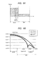
- Fig. 6 comprises views for explaining the distribution of impurities in the depth direction of a substrate SUB.
- Fig. 6A shows the distribution of impurities in a substrate SUB before the substrate SUB is subjected to heat treatment and
- Fig. 6B shows the result of simulating the distribution of the impurities in the substrate SUB after the substrate SUB is subjected to heat treatment.
- a base substrate BSUB contains p-type impurities of a high concentration and an epitaxial layer EPI contains p-type impurities of a concentration lower than that of the base substrate BSUB. Then an n-type second embedded layer BINPL2 is formed in the region of the epitaxial layer EPI touching the base substrate BSUB.
- the p-type impurities contained in the base substrate BSUB comprise B for example and the n-type impurities contained in the second embedded layer BINPL2 comprise P for example.
- the second embedded layer BINPL2 is defined as the region where an n-type impurity concentration is higher than a p-type impurity concentration.
- the second embedded layer BINPL2 according to the definition is located on the side closer to the surface of the epitaxial layer EPI than the second embedded layer BINPL2 in the state of Fig. 6A .
- the second embedded layer BINPL2 when the second embedded layer BINPL2 is not formed in the state of Fig. 6A , the p-type impurities in the base substrate BSUB diffuse into the epitaxial layer EPI and hence the withstand voltage between the base substrate BSUB and a first embedded layer BINPL1 deteriorates.
- the second embedded layer BINPL2 since the second embedded layer BINPL2 is formed, the p-type impurities diffusing from the base substrate BSUB to the epitaxial layer EPI are offset by the n-type impurities contained in the second embedded layer BINPL2. As a result, the withstand voltage between the base substrate BSUB and a first embedded layer BINPL1 is inhibited from deteriorating.
- the epitaxial layer EPI is a silicon layer for example
- the thermal diffusion rate of P is nearly identical to the thermal diffusion rate of B at about 1,000°C. Consequently, the offset effect is particularly large when B is elected as the p-type impurities contained in the base substrate BSUB and P is selected as the n-type impurities contained in the second embedded layer BINPL2.
- the second embedded layer BINPL2 is formed so as to be deeper than the element isolation trenches SDTR. As a result, it is possible to bring the second embedded layer BINPL2 closer to the base substrate BSUB. As a result, it is possible to effectively offset the impurities diffusing from the base substrate BSUB to the epitaxial layer EPI.
- Fig. 7 comprises sectional views showing a manufacturing method of a semiconductor device SD according to Second Embodiment.
- a base substrate BSUB is prepared.
- n-type impurities are injected into the base substrate BSUB by thermal diffusion or ion implantation.
- a second embedded layer BINPL2 is formed in the surface layer of the base substrate BSUB.
- an epitaxial layer EPI is formed over the base substrate BSUB.
- the method for forming the epitaxial layer EPI is the same as the method for forming an epitaxial layer EPI in First Embodiment except that the second embedded layer BINPL2 is not formed.
- Fig. 8 comprises views for explaining the distribution of impurities in the depth direction of a substrate SUB according to the present embodiment and corresponds to Fig. 6 in First Embodiment.
- Fig. 8A shows the distribution of impurities in a substrate SUB before the substrate SUB is subjected to heat treatment and
- Fig. 8B shows the result of simulating the distribution of the impurities in the substrate SUB after the substrate SUB is subjected to heat treatment.
- a second embedded layer BINPL2 is formed in the surface layer of a base substrate BSUB.
- the second embedded layer BINPL2 is defined as the region where the concentration of n-type impurities is higher than the concentration of p-type impurities in the same manner as First Embodiment.
- the second embedded layer BINPL2 according to the definition is located inside an epitaxial layer EPI in the example shown in the figure.
- the second embedded layer BINPL2 is formed in the substrate SUB and hence it is possible to inhibit the withstand voltage between the base substrate BSUB and a first embedded layer BINPL1 from deteriorating.
- Fig. 9 is a sectional view showing the configuration of a semiconductor device SD according to Third Embodiment.
- the semiconductor device SD according to the present embodiment has a configuration similar to the semiconductor device SD according to Second Embodiment except that the semiconductor device SD according to the present embodiment has a third embedded layer BINPL3 instead of a second embedded layer BINPL2.
- the third embedded layer BINPL3 is a layer into which an element (hereunder described as a diffusion inhibiting element) to inhibit impurities in a base substrate BSUB from thermally diffusing is introduced.
- the third embedded layer BINPL3 is formed by introducing a diffusion inhibiting element into the surface layer of the base substrate BSUB instead of n-type impurities in Fig. 7A of Second Embodiment.
- the diffusion inhibiting element is at least one of N, C, and O for example.
- the concentration of the diffusion inhibiting element in the third embedded layer BINPL3 is identical to or lower than the concentration of the p-type impurities in the base substrate BSUB and higher than the concentration of the p-type impurities in an epitaxial layer EPI, for example.
- Fig. 10 comprises views for explaining the distribution of impurities in the depth direction of a substrate SUB according to the present embodiment and corresponds to Fig. 8 in Second Embodiment.
- Fig. 10A shows the distribution of impurities in a substrate SUB before the substrate SUB is subjected to heat treatment and
- Fig. 10B shows the distribution of the impurities in the substrate SUB after the substrate SUB is subjected to heat treatment.
- a third embedded layer BINPL3 is formed in the surface layer of a base substrate BSUB.
- impurities in the base substrate BSUB diffuse toward an epitaxial layer EPI but the quantity of the diffusion is small because the third embedded layer BINPL3 is formed.
- a diffusion inhibiting element in the third embedded layer BINPL3 also diffuses in the substrate SUB. As a result, the width of the third embedded layer BINPL3 increases.
- the third embedded layer BINPL3 is formed in the substrate SUB and hence the impurities in the base substrate BSUB hardly diffuse toward the epitaxial layer EPI. As a result, it is possible to inhibit the withstand voltage between the base substrate BSUB and a first embedded layer BINPL1 from deteriorating.
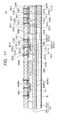
- Fig. 11 is a sectional view showing the configuration of a semiconductor device SD according to Fourth Embodiment.
- the semiconductor device SD according to the present embodiment has a configuration similar to any one of First to Third Embodiments except that the semiconductor device SD according to the present embodiment has a backside electrode EL instead of an embedded contact BCON.
- the figure shows the case of a configuration similar to First Embodiment.
- the backside electrode EL is formed over the surface of a base substrate BSUB where an epitaxial layer EPI is not formed and gives a fixed potential to the base substrate BSUB.
- the backside electrode EL comprises a metal such as Al for example.
- the backside electrode EL is formed by a sputtering method for example.
Landscapes
- Insulated Gate Type Field-Effect Transistor (AREA)
- Metal-Oxide And Bipolar Metal-Oxide Semiconductor Integrated Circuits (AREA)
- Electrodes Of Semiconductors (AREA)
- Element Separation (AREA)
Abstract
Description
- The disclosure of Japanese Patent Application No.
2014-107950 filed on May 26, 2014 - The present invention relates to a semiconductor device and is, for example, a technology applicable to a semiconductor device having a diffusion layer embedded into a substrate.
- In a semiconductor device, it sometimes happens that a diffusion layer is embedded into a substrate and a transistor is formed over the diffusion layer. In the transistor, a substance formed by epitaxially growing a semiconductor layer over a semiconductor substrate acting as a base is used as the substrate for example. Then the diffusion layer is: formed by an ion implantation method after the semiconductor layer is formed in some cases; or formed when the semiconductor layer is epitaxially grown in other cases.
- Meanwhile, Japanese Unexamined Patent Application Publication No.
Sho 62 (1987)-40719 - Further, Japanese Unexamined Patent Application Publication No.
2002-176177 2002-176177 - When a semiconductor layer is formed over a substrate acting as a base, a diffusion layer is embedded into the semiconductor layer, and a transistor is formed over the diffusion layer, the withstand voltage of the transistor is dominated by the distance between the substrate acting as the base and the diffusion layer in some cases. Since impurities are also introduced into the substrate however, there has been the possibility that the impurities diffuse from the substrate to the semiconductor layer in the manufacturing process of a semiconductor device and the withstand voltage of the transistor deteriorates. Other problems and novel features will be obvious from the descriptions and attached drawings in the present specification.
- According to an embodiment, a first electrically conductive type semiconductor layer is formed over a first electrically conductive type base substrate. The impurity concentration of the semiconductor layer is lower than that of the base substrate. A second electrically conductive type first embedded layer and a second electrically conductive type second embedded layer are formed in the semiconductor layer. The second embedded layer is deeper than the first embedded layer, is kept away from the first embedded layer, and has an impurity concentration lower than the first embedded layer. A transistor is further formed in the semiconductor layer.
- According to the embodiment, it is possible to inhibit: impurities from diffusing from the substrate to the semiconductor layer; and the withstand voltage of the transistor from deteriorating.
- In the drawings:
-
Fig. 1 is a sectional view showing the configuration of a semiconductor device according to First Embodiment. -
Fig. 2 is a plan view of a transistor. -
Fig. 3 is a sectional view showing a manufacturing method of a semiconductor device. -
Fig. 4 is a sectional view showing the manufacturing method of the semiconductor device. -
Fig. 5 is a sectional view showing the manufacturing method of the semiconductor device. -
Fig. 6 comprises views for explaining the distribution of impurities in the depth direction of a substrate. -
Fig. 7 comprises sectional views showing a manufacturing method of a semiconductor device according to Second Embodiment. -
Fig. 8 comprises views for explaining the distribution of impurities in the depth direction of a substrate. -
Fig. 9 is a sectional view showing the configuration of a semiconductor device according to Third Embodiment. -
Fig. 10 comprises views for explaining the distribution of impurities in the depth direction of a substrate. -
Fig. 11 is a sectional view showing the configuration of a semiconductor device according to Fourth Embodiment. - Embodiments are explained in reference to the drawings hereunder. In all the drawings, similar constituent components are represented by similar reference numerals and explanations are omitted appropriately.
-
Fig. 1 is a sectional view showing the configuration of a semiconductor device SD according to First Embodiment. The semiconductor device SD according to the present embodiment is formed by using a substrate SUB. The substrate SUB is formed by growing an epitaxial layer EPI (semiconductor layer) comprising a semiconductor (for example silicon) over a base substrate BSUB comprising a bulk semiconductor (for example monocrystal silicon). Both the base substrate BSUB and the epitaxial layer EPI are an identical electrically conductive type (first electrically conductive type: for example P-type). The impurity concentration of the base substrate BSUB is higher than that of the epitaxial layer EPI. - A first embedded layer BINPL1 that is an electrically conductive type (second electrically conductive type: for example n-type) different from the epitaxial layer EPI is formed in the epitaxial layer EPI. The first embedded layer BINPL1 is kept away from the base substrate BSUB. The first embedded layer BINPL1: either may be formed when the epitaxial layer EPI is grown epitaxially; or may be formed by an ion implantation method after the epitaxial layer EPI is formed. In the former case, the first embedded layer BINPL1 is formed over the whole surface of the substrate SUB.
- Further, a second embedded layer BINPL2 is formed in the epitaxial layer EPI. The second embedded layer BINPL2 is a second electrically conductive type impurity layer, is deeper than the first embedded layer BINPL1, and is kept away from the first embedded layer BINPL1. The impurity concentration of the second embedded layer BINPL2 is lower than that of the first embedded layer BINPL1. The second embedded layer BINPL2 is formed in order to inhibit: the impurities of the base substrate BSUB from diffusing in the epitaxial layer EPI; and the first electrically conductive type impurity concentration in the lower layer of the epitaxial layer EPI from increasing.
- Then transistors TR2 and TR3 constituting a logic circuit and a transistor TR1 for electric power control are formed in the epitaxial layer EPI. At least the transistor TR1 overlaps with the first embedded layer BINPL1 in a planar view.
- The following explanations are based on the case where the first electrically conductive type is a p-type and the second electrically conductive type is an n-type. It is also possible however that the first electrically conductive type is an n-type and the second electrically conductive type is a p-type.
- The transistor TR2 is an n-type low withstand voltage transistor and has a gate electrode GE2, a source SOU2, and a drain DRN2. The transistor TR3 is a p-type low withstand voltage transistor and has a gate electrode GE3, a source SOU3, and a drain DRN3. The transistors TR2 and TR3 include a CMOS transistor. Meanwhile, a gate insulating film (not shown in the figure) is formed under the gate electrodes GE2 and GE3.
- The transistor TR1 is a horizontal transistor for electric power control and has a withstand voltage higher than the transistors TR2 and TR3. The transistor TR1 has a gate electrode GE1, a source SOU1, and a drain DRN1. The distance between the drain DRN1 and the gate electrode GE1 is larger than the distance between the source SOU1 and the gate electrode GE1. As a result, the withstand voltage between the drain DRN1 and the gate electrode GE1 is higher. A gate insulating film (not shown in the figure) is formed under the gate electrode GE1. The gate insulating film is thicker than the gate insulating film of the transistors TR2 and TR3. Here, an element isolation insulating film formed by an STI method or a LOCOS method is formed between the drain DRN1 and the gate electrode GE1.
- The drain DRN1 has an n-type well WL12 and an n-type high concentration region HINPL13 formed over the surface layer of the n-type well WL12. The high concentration region HINPL13 is coupled to a contact CON3. Further, an n--type offset region NOF11 is formed around the n-type well WL12. In other words, the n-type well WL12 is formed in the surface layer of the offset region NOF11.
- Meanwhile, the source SOU1 has an n-type high concentration region HINPL12. The high concentration region HINPL12 is formed in the surface layer of a p-type well WL21. Although it is not shown in the figure, a p-type high concentration region is formed at a part of the p-type well WL21 located adjacent to the high concentration region HINPL12. Then a contact CON2 is coupled to the p-type high concentration region and the high concentration region HINPL12.
- Then an insulating film HMSK1 and an interlayer insulating film INSL1 are formed over the substrate SUB. The insulating film HMSK1 is a silicon nitride film for example and the interlayer insulating film INSL1 is a silicon oxide film for example. Contacts CON2, CON3, CON4, CON5, CON6, and CON7 are embedded into the insulating film HMSK1 and the interlayer insulating film INSL1. The contact CON2 is coupled to the source SOU1 of the transistor TR1 and the contact CON3 is coupled to the drain DRN1 of the transistor TR1. The contact CON4 is coupled to the source SOU2 of the transistor TR2 and the contact CON5 is coupled to the drain DRN2 of the transistor TR2. The contact CON6 is coupled to the source SOU3 of the transistor TR3 and the contact CON7 is coupled to the drain DRN3 of the transistor TR3. Meanwhile, although they are not shown in the figure, a contact coupled to the gate electrode GE1, a contact coupled to the gate electrode GE2, a contact coupled to the gate electrode GE3, and a contact coupled to a deep well DWL (described later) are also embedded into the insulating film HMSK1 and the interlayer insulating film INSL1.
- Wires INC2, INC3, INC4, INC5, INC6, and INC7 are formed over the interlayer insulating film INSL1. The wires INC2, INC3, INC4, INC5, INC6, and INC7 comprise a metal such as aluminum for example and are coupled to the contacts CON2, CON3, CON4, CON5, CON6, and CON7 respectively. Meanwhile, wires (not shown in the figure) coupled to the respective gate electrodes and a wire (not shown in the figure) coupled to the deep well DWL are also formed over the interlayer insulating film INSL1.
- The transistor TR1 is formed in a first element region EL1 and the transistors TR2 and TR3 are formed in a second element region EL2. More specifically, the single transistor TR1 is formed in the first element region EL1. In contrast, the plural transistors TR2 and TR3 are formed in the second element region EL2. Meanwhile, in
Fig. 1 , only a pair of the transistors TR2 and TR3 are shown in the second element region EL2 for the simplification of the figure. Then the first element region EL1 and the second element region EL2 are surrounded by element isolation trenches SDTR respectively. The element isolation trenches SDTR pass through the first embedded layer BINPL1 but do not reach the base substrate BSUB. Further in the example shown in the figure, the bottom parts of the element isolation trenches SDTR do not reach even the second embedded layer BINPL2. In other words, the element isolation trenches SDTR are formed so as to be shallower than the second embedded layer BINPL2. - Then an embedded insulating film BINSL is embedded into the element isolation trenches SDTR. In the example shown in the figure, the embedded insulating film BINSL is a part of the interlayer insulating film INSL1 over the substrate SUB.
- Meanwhile, the n-type deep well DWL and an embedded contact BCON are further formed in the substrate SUB. The bottom face of the deep well DWL reaches the first embedded layer BINPL1 and the deep well DWL gives a fixed potential to the first embedded layer BINPL1. The embedded contact BCON is a contact embedded into the substrate SUB and passes through the first embedded layer BINPL1 and the second embedded layer BINPL2. As a result, a fixed potential is given by the embedded contact BCON to the epitaxial layer EPI and the base substrate BSUB under the second embedded layer BINPL2.
- In the example shown in the figure, a p-type impurity region INPL1 is formed in the region of the epitaxial layer EPI touching the bottom face of the embedded contact BCON. The impurity concentration of the impurity region INPL1 is higher than that of the epitaxial layer EP1. The contact resistance between the embedded contact BCON and the epitaxial layer EP1 decreases by forming the impurity region INPL1.
- A groove (or hole) into which the embedded contact BCON is embedded is formed through the same process as a contact hole into which the contact CON2 is embedded for example. The groove (or hole) may otherwise be formed through an independent process. An insulating film (thermally-oxidized film for example) INSL2 is formed over the inner face of the groove. As a result, the embedded contact BCON is insulated from the first embedded layer BINPL1 and the part of the epitaxial layer EPI located above the first embedded layer BINPL1. Further, the embedded contact BCON is formed through the same process as the contact CON2 and other contacts. As a result, the embedded contact BCON passes through the interlayer insulating film INSL1 and the insulating film HMSK1 and the top end is coupled to a wire INC8 over the interlayer insulating film INSL1.
- Meanwhile, the potential of the first embedded layer BINPL1 may be either a floating potential or a fixed potential. In the latter case, an impurity region for raising the first embedded layer BINPL1 electrically to the surface layer of the epitaxial layer EPI is formed in the epitaxial layer EPI. The lower part of the impurity region is coupled to the first embedded layer BINPL1 and a contact is coupled to the upper part of the impurity region.
-
Fig. 2 is a plan view of a transistor TR1. A gate electrode GE1 surrounds an n-type well WL12 of a drain DRN1 and a p-type well WL21 surrounds the gate electrode GE1. Then an element isolation trench SDTR is formed along the sides of a polygon (rectangle in the example shown in the figure) and surrounds the p-type well WL21. In other words, the transistor TR1 is located inside the element isolation trench SDTR. -
Figs. 3 to 5 are sectional views showing a manufacturing method of a semiconductor device SD. The figures correspond toFig. 1 . - Firstly, as shown in
Fig. 3 , a base substrate BSUB is prepared. Successively, an epitaxial layer EPI is formed over the base substrate BSUB. On this occasion, a second embedded layer BINPL2 and a first embedded layer BINPL1 are formed by switching gases for introducing impurities in midstream. At the step, the second embedded layer BINPL2 is located immediately over the base substrate BSUB (in other words, at the lowermost layer of the epitaxial layer EPI) for example. - Successively, as shown in
Fig. 4 , various kinds of wells (including a deep well DWL) and an offset region NOF11 are formed in the epitaxial layer EPI by an ion implantation method for example. Successively, a groove is formed in the epitaxial layer EPI and an insulating film, a silicon oxide film for example, is embedded into the groove. As a result, an element isolation insulating film (not shown in the figure) is formed. Meanwhile, the various wells and the offset region NOF11 may otherwise be formed after the element isolation insulating film is formed. - Successively, a gate insulating film for transistors TR1, TR2, and TR3 is formed. Successively, a film (polysilicon film for example) as a material for gate electrodes is formed and the film is selectively removed. As a result, gate electrodes GE1, GE2, and GE3 are formed. Successively, high concentration regions (HINPL12 and HINPL13 for example) are formed in the epitaxial layer EPI by an ion implantation method for example.
- Meanwhile, sidewalls may be formed over the side faces of the gate electrodes GE1, GE2, and GE3 in some cases. In such a case, the high concentration regions are formed after the sidewalls are formed.
- Further, heat treatment is applied after the high concentration regions are formed in the epitaxial layer EPI. Impurities diffuse by the heat treatment and as a result the second embedded layer BINPL2 gets away from the base substrate BSUB.
- Successively, as shown in
Fig. 5 , an insulating film HMSK1 is formed over the epitaxial layer EPI. Successively, a resist pattern (not shown in the figure) is formed over the insulating film HMSK1. The resist pattern has openings in the region where element isolation trenches SDTR are to be formed. Successively, the insulating film HMSK1 is etched with the resist pattern used as a mask. As a result, the openings are formed in the region of the insulating film HMSK1 where the element isolation trenches SDTR are to be formed. - Successively, the epitaxial layer EPI (also the element isolation insulating film in some locations) is etched with the insulating film HMSK1 used as a mask. As a result, the element isolation trenches SDTR are formed. When the resist pattern remains thereafter, the resist pattern is removed.
- Successively, an interlayer insulating film INSL1 is formed. On this occasion, parts of the interlayer insulating film INSL1 are embedded into the element isolation trenches SDTR and come to be an embedded insulating film BINSL. On this occasion, voids may be formed in the element isolation trenches SDTR in some cases. Since the voids are occluded with the interlayer insulating film INSL1 (embedded insulating film BINSL) and are not exposed even at the succeeding processes however, the voids do not influence the quality of the semiconductor device SD.
- Successively, a resist pattern (not shown in the figure) is formed over the interlayer insulating film INSL1 and the interlayer insulating film INSL1 is etched with the resist pattern used as a mask. As a result, contact holes for forming contacts are formed. In the process, a contact hole is also formed in the region of the interlayer insulating film INSL1 where an embedded contact BCON is to be formed. The contact hole reaches down to the bottom of a groove formed in the epitaxial layer EPI. Impurities are injected into the contact hole. As a result, an impurity region INPL1 is formed. Then a metal such as W is embedded into the contact holes. As a result, the contacts and the embedded contact BCON are formed.
- Successively, a metal film (A1 for example) is formed over the interlayer insulating film INSL1. Successively, the metal film is selectively removed. As a result, wires are formed.
-
Fig. 6 comprises views for explaining the distribution of impurities in the depth direction of a substrate SUB.Fig. 6A shows the distribution of impurities in a substrate SUB before the substrate SUB is subjected to heat treatment andFig. 6B shows the result of simulating the distribution of the impurities in the substrate SUB after the substrate SUB is subjected to heat treatment. - As shown in
Fig. 6A , a base substrate BSUB contains p-type impurities of a high concentration and an epitaxial layer EPI contains p-type impurities of a concentration lower than that of the base substrate BSUB. Then an n-type second embedded layer BINPL2 is formed in the region of the epitaxial layer EPI touching the base substrate BSUB. Here, the p-type impurities contained in the base substrate BSUB comprise B for example and the n-type impurities contained in the second embedded layer BINPL2 comprise P for example. - When the substrate SUB shown in
Fig. 6A is subjected to heat treatment, the impurities contained in the respective layers diffuse thermally. In the state after heat treatment, the second embedded layer BINPL2 is defined as the region where an n-type impurity concentration is higher than a p-type impurity concentration. The second embedded layer BINPL2 according to the definition is located on the side closer to the surface of the epitaxial layer EPI than the second embedded layer BINPL2 in the state ofFig. 6A . - Meanwhile, when the second embedded layer BINPL2 is not formed in the state of
Fig. 6A , the p-type impurities in the base substrate BSUB diffuse into the epitaxial layer EPI and hence the withstand voltage between the base substrate BSUB and a first embedded layer BINPL1 deteriorates. - In the present embodiment in contrast, since the second embedded layer BINPL2 is formed, the p-type impurities diffusing from the base substrate BSUB to the epitaxial layer EPI are offset by the n-type impurities contained in the second embedded layer BINPL2. As a result, the withstand voltage between the base substrate BSUB and a first embedded layer BINPL1 is inhibited from deteriorating. Here, when the epitaxial layer EPI is a silicon layer for example, the thermal diffusion rate of P is nearly identical to the thermal diffusion rate of B at about 1,000°C. Consequently, the offset effect is particularly large when B is elected as the p-type impurities contained in the base substrate BSUB and P is selected as the n-type impurities contained in the second embedded layer BINPL2.
- Further, the second embedded layer BINPL2 is formed so as to be deeper than the element isolation trenches SDTR. As a result, it is possible to bring the second embedded layer BINPL2 closer to the base substrate BSUB. As a result, it is possible to effectively offset the impurities diffusing from the base substrate BSUB to the epitaxial layer EPI.
-
Fig. 7 comprises sectional views showing a manufacturing method of a semiconductor device SD according to Second Embodiment. Firstly, as shown inFig. 7A , a base substrate BSUB is prepared. Successively, n-type impurities are injected into the base substrate BSUB by thermal diffusion or ion implantation. As a result, a second embedded layer BINPL2 is formed in the surface layer of the base substrate BSUB. - Successively, an epitaxial layer EPI is formed over the base substrate BSUB. The method for forming the epitaxial layer EPI is the same as the method for forming an epitaxial layer EPI in First Embodiment except that the second embedded layer BINPL2 is not formed.
- The succeeding processes are the same as First Embodiment.
-
Fig. 8 comprises views for explaining the distribution of impurities in the depth direction of a substrate SUB according to the present embodiment and corresponds toFig. 6 in First Embodiment.Fig. 8A shows the distribution of impurities in a substrate SUB before the substrate SUB is subjected to heat treatment andFig. 8B shows the result of simulating the distribution of the impurities in the substrate SUB after the substrate SUB is subjected to heat treatment. - As shown in
Fig. 8A , in the state before heat treatment, a second embedded layer BINPL2 is formed in the surface layer of a base substrate BSUB. As shown inFig. 8B in contrast, when a substrate SUB is subjected to heat treatment, the second embedded layer BINPL2 is defined as the region where the concentration of n-type impurities is higher than the concentration of p-type impurities in the same manner as First Embodiment. The second embedded layer BINPL2 according to the definition is located inside an epitaxial layer EPI in the example shown in the figure. - In the present embodiment too, the second embedded layer BINPL2 is formed in the substrate SUB and hence it is possible to inhibit the withstand voltage between the base substrate BSUB and a first embedded layer BINPL1 from deteriorating.
-
Fig. 9 is a sectional view showing the configuration of a semiconductor device SD according to Third Embodiment. The semiconductor device SD according to the present embodiment has a configuration similar to the semiconductor device SD according to Second Embodiment except that the semiconductor device SD according to the present embodiment has a third embedded layer BINPL3 instead of a second embedded layer BINPL2. - The third embedded layer BINPL3 is a layer into which an element (hereunder described as a diffusion inhibiting element) to inhibit impurities in a base substrate BSUB from thermally diffusing is introduced. The third embedded layer BINPL3 is formed by introducing a diffusion inhibiting element into the surface layer of the base substrate BSUB instead of n-type impurities in
Fig. 7A of Second Embodiment. The diffusion inhibiting element is at least one of N, C, and O for example. The concentration of the diffusion inhibiting element in the third embedded layer BINPL3 is identical to or lower than the concentration of the p-type impurities in the base substrate BSUB and higher than the concentration of the p-type impurities in an epitaxial layer EPI, for example. -
Fig. 10 comprises views for explaining the distribution of impurities in the depth direction of a substrate SUB according to the present embodiment and corresponds toFig. 8 in Second Embodiment.Fig. 10A shows the distribution of impurities in a substrate SUB before the substrate SUB is subjected to heat treatment andFig. 10B shows the distribution of the impurities in the substrate SUB after the substrate SUB is subjected to heat treatment. - As shown in
Fig. 10A , in the state before heat treatment, a third embedded layer BINPL3 is formed in the surface layer of a base substrate BSUB. As shown inFig. 10B in contrast, when the substrate SUB is subjected to heat treatment, impurities in the base substrate BSUB diffuse toward an epitaxial layer EPI but the quantity of the diffusion is small because the third embedded layer BINPL3 is formed. Here, a diffusion inhibiting element in the third embedded layer BINPL3 also diffuses in the substrate SUB. As a result, the width of the third embedded layer BINPL3 increases. - In the present embodiment, the third embedded layer BINPL3 is formed in the substrate SUB and hence the impurities in the base substrate BSUB hardly diffuse toward the epitaxial layer EPI. As a result, it is possible to inhibit the withstand voltage between the base substrate BSUB and a first embedded layer BINPL1 from deteriorating.
-
Fig. 11 is a sectional view showing the configuration of a semiconductor device SD according to Fourth Embodiment. The semiconductor device SD according to the present embodiment has a configuration similar to any one of First to Third Embodiments except that the semiconductor device SD according to the present embodiment has a backside electrode EL instead of an embedded contact BCON. The figure shows the case of a configuration similar to First Embodiment. - The backside electrode EL is formed over the surface of a base substrate BSUB where an epitaxial layer EPI is not formed and gives a fixed potential to the base substrate BSUB. The backside electrode EL comprises a metal such as Al for example. The backside electrode EL is formed by a sputtering method for example.
- In the present embodiment too, it is possible to inhibit the withstand voltage between the base substrate BSUB and a first embedded layer BINPL1 from deteriorating.
- Although the invention established by the present inventors has heretofore been explained concretely on the basis of the embodiments, it goes without saying that the present invention is not limited to the embodiments and can be modified variously within the scope not departing from the tenor of the invention.
Claims (5)
- A semiconductor device having: a first electrically conductive type base substrate; a first electrically conductive type semiconductor layer being formed over the base substrate and having an impurity concentration lower than the base substrate; a second electrically conductive type first embedded layer formed in the semiconductor layer; a second embedded layer being formed in the semiconductor layer, being deeper than the first embedded layer, being kept away from the first embedded layer, and having an impurity concentration lower than the first embedded layer; and transistors formed in the semiconductor layer.
- A semiconductor device according to Claim 1,
wherein the semiconductor device has trenches being formed in the semiconductor layer and surrounding the transistors and an insulating film embedded into the trenches; and the bottom faces of the trenches are located at positions shallower than the second embodiment layer. - A semiconductor device according to Claim 1,
wherein the semiconductor device has a hole formed in the semiconductor layer, an insulating layer formed over the side face of the hole, and a conductor embedded into the hole; and the bottom face of the hole is deeper than the second embedded layer. - A semiconductor device according to Claim 3,
wherein the semiconductor device has a first electrically conductive type region being formed in the semiconductor layer, being located at the bottom part of the hole, and having an impurity concentration higher than the semiconductor layer. - A semiconductor device according to Claim 1,
wherein P is introduced into the second embedded layer and B is introduced into the base substrate.
Applications Claiming Priority (1)
| Application Number | Priority Date | Filing Date | Title |
|---|---|---|---|
| JP2014107950A JP6300638B2 (en) | 2014-05-26 | 2014-05-26 | Semiconductor device |
Publications (1)
| Publication Number | Publication Date |
|---|---|
| EP2950339A1 true EP2950339A1 (en) | 2015-12-02 |
Family
ID=53002622
Family Applications (1)
| Application Number | Title | Priority Date | Filing Date |
|---|---|---|---|
| EP15165397.9A Withdrawn EP2950339A1 (en) | 2014-05-26 | 2015-04-28 | Semiconductor device |
Country Status (6)
| Country | Link |
|---|---|
| US (2) | US10062773B2 (en) |
| EP (1) | EP2950339A1 (en) |
| JP (1) | JP6300638B2 (en) |
| KR (1) | KR20150136015A (en) |
| CN (1) | CN105140223A (en) |
| TW (1) | TW201606939A (en) |
Cited By (1)
| Publication number | Priority date | Publication date | Assignee | Title |
|---|---|---|---|---|
| DE102017102127A1 (en) | 2017-02-03 | 2018-08-09 | Infineon Technologies Ag | A method of manufacturing semiconductor devices using epitaxy and semiconductor devices having a lateral structure |
Citations (10)
| Publication number | Priority date | Publication date | Assignee | Title |
|---|---|---|---|---|
| JPS5887866A (en) * | 1981-11-20 | 1983-05-25 | Hitachi Ltd | semiconductor equipment |
| JPS6240719A (en) | 1985-08-16 | 1987-02-21 | Nec Corp | Manufacture of epitaxial wafer |
| JP2002176177A (en) | 2000-12-07 | 2002-06-21 | Denso Corp | Semiconductor device and its manufacturing method |
| EP1335425A1 (en) * | 2000-10-23 | 2003-08-13 | Sharp Kabushiki Kaisha | Semiconductor device and its production method |
| US6664608B1 (en) * | 2001-11-30 | 2003-12-16 | Sun Microsystems, Inc. | Back-biased MOS device |
| US20060220140A1 (en) * | 2005-04-01 | 2006-10-05 | Semiconductor Components Industries, Llc. | Method of forming an integrated power device and structure |
| US20090230468A1 (en) * | 2008-03-17 | 2009-09-17 | Jun Cai | Ldmos devices with improved architectures |
| US20100052052A1 (en) * | 2004-01-29 | 2010-03-04 | Enpirion, Incorporated | Integrated Circuit with a Laterally Diffused Metal Oxide Semiconductor Device and Method of Forming the Same |
| JP2010232673A (en) * | 2010-06-07 | 2010-10-14 | Fuji Electric Systems Co Ltd | Semiconductor device |
| EP2341538A2 (en) * | 2009-12-30 | 2011-07-06 | Intersil Americas Inc. | Voltage converter with integrated Schottky device and systems including same |
Family Cites Families (18)
| Publication number | Priority date | Publication date | Assignee | Title |
|---|---|---|---|---|
| JPH0364029A (en) * | 1989-08-02 | 1991-03-19 | Hitachi Ltd | Semiconductor device and its manufacturing method |
| JPH10125916A (en) * | 1996-10-24 | 1998-05-15 | Matsushita Electric Ind Co Ltd | Semiconductor device and manufacture thereof |
| JP4528460B2 (en) * | 2000-06-30 | 2010-08-18 | 株式会社東芝 | Semiconductor element |
| JP4728508B2 (en) * | 2001-06-11 | 2011-07-20 | 株式会社東芝 | Method for manufacturing vertical power semiconductor device |
| US6916330B2 (en) * | 2001-10-30 | 2005-07-12 | Depuy Spine, Inc. | Non cannulated dilators |
| US6734493B2 (en) * | 2002-02-08 | 2004-05-11 | Taiwan Semiconductor Manufacturing Co., Ltd. | Lateral double diffused metal oxide semiconductor (LDMOS) device with aligned buried layer isolation layer |
| US6943426B2 (en) * | 2002-08-14 | 2005-09-13 | Advanced Analogic Technologies, Inc. | Complementary analog bipolar transistors with trench-constrained isolation diffusion |
| JP4437388B2 (en) * | 2003-02-06 | 2010-03-24 | 株式会社リコー | Semiconductor device |
| TWI223442B (en) * | 2003-09-02 | 2004-11-01 | Nanya Technology Corp | DRAM cell array and its manufacturing method |
| JP5164333B2 (en) * | 2005-12-28 | 2013-03-21 | オンセミコンダクター・トレーディング・リミテッド | Semiconductor device |
| JP2007221024A (en) * | 2006-02-20 | 2007-08-30 | Toshiba Corp | Semiconductor device |
| JP4800862B2 (en) * | 2006-06-21 | 2011-10-26 | 株式会社日立製作所 | phantom |
| JP4798119B2 (en) * | 2007-11-06 | 2011-10-19 | 株式会社デンソー | Silicon carbide semiconductor device and manufacturing method thereof |
| JP4577355B2 (en) * | 2007-12-26 | 2010-11-10 | 株式会社デンソー | Silicon carbide semiconductor device and manufacturing method thereof |
| CN102376548A (en) * | 2010-08-26 | 2012-03-14 | 上海华虹Nec电子有限公司 | Method for reducing auto-doping and external diffusion in epitaxial process |
| CN103210520B (en) * | 2010-10-04 | 2017-03-08 | 达纳加拿大公司 | Conformal fluid-cooled heat exchanger for batteries |
| JP2012169384A (en) * | 2011-02-11 | 2012-09-06 | Denso Corp | Silicon carbide semiconductor device and method of manufacturing the same |
| US9287371B2 (en) * | 2012-10-05 | 2016-03-15 | Semiconductor Components Industries, Llc | Semiconductor device having localized charge balance structure and method |
-
2014
- 2014-05-26 JP JP2014107950A patent/JP6300638B2/en active Active
-
2015
- 2015-04-28 EP EP15165397.9A patent/EP2950339A1/en not_active Withdrawn
- 2015-05-14 US US14/712,894 patent/US10062773B2/en active Active
- 2015-05-21 KR KR1020150071077A patent/KR20150136015A/en not_active Withdrawn
- 2015-05-22 TW TW104116362A patent/TW201606939A/en unknown
- 2015-05-25 CN CN201510272590.8A patent/CN105140223A/en active Pending
-
2018
- 2018-06-26 US US16/019,047 patent/US20180308964A1/en not_active Abandoned
Patent Citations (10)
| Publication number | Priority date | Publication date | Assignee | Title |
|---|---|---|---|---|
| JPS5887866A (en) * | 1981-11-20 | 1983-05-25 | Hitachi Ltd | semiconductor equipment |
| JPS6240719A (en) | 1985-08-16 | 1987-02-21 | Nec Corp | Manufacture of epitaxial wafer |
| EP1335425A1 (en) * | 2000-10-23 | 2003-08-13 | Sharp Kabushiki Kaisha | Semiconductor device and its production method |
| JP2002176177A (en) | 2000-12-07 | 2002-06-21 | Denso Corp | Semiconductor device and its manufacturing method |
| US6664608B1 (en) * | 2001-11-30 | 2003-12-16 | Sun Microsystems, Inc. | Back-biased MOS device |
| US20100052052A1 (en) * | 2004-01-29 | 2010-03-04 | Enpirion, Incorporated | Integrated Circuit with a Laterally Diffused Metal Oxide Semiconductor Device and Method of Forming the Same |
| US20060220140A1 (en) * | 2005-04-01 | 2006-10-05 | Semiconductor Components Industries, Llc. | Method of forming an integrated power device and structure |
| US20090230468A1 (en) * | 2008-03-17 | 2009-09-17 | Jun Cai | Ldmos devices with improved architectures |
| EP2341538A2 (en) * | 2009-12-30 | 2011-07-06 | Intersil Americas Inc. | Voltage converter with integrated Schottky device and systems including same |
| JP2010232673A (en) * | 2010-06-07 | 2010-10-14 | Fuji Electric Systems Co Ltd | Semiconductor device |
Cited By (3)
| Publication number | Priority date | Publication date | Assignee | Title |
|---|---|---|---|---|
| DE102017102127A1 (en) | 2017-02-03 | 2018-08-09 | Infineon Technologies Ag | A method of manufacturing semiconductor devices using epitaxy and semiconductor devices having a lateral structure |
| US10276656B2 (en) | 2017-02-03 | 2019-04-30 | Infineon Technologies Ag | Method of manufacturing semiconductor devices by using epitaxy and semiconductor devices with a lateral structure |
| DE102017102127B4 (en) | 2017-02-03 | 2023-03-09 | Infineon Technologies Ag | Method of manufacturing semiconductor devices using epitaxy and semiconductor devices with a lateral structure |
Also Published As
| Publication number | Publication date |
|---|---|
| US20180308964A1 (en) | 2018-10-25 |
| US10062773B2 (en) | 2018-08-28 |
| CN105140223A (en) | 2015-12-09 |
| KR20150136015A (en) | 2015-12-04 |
| TW201606939A (en) | 2016-02-16 |
| US20150340479A1 (en) | 2015-11-26 |
| JP2015225877A (en) | 2015-12-14 |
| JP6300638B2 (en) | 2018-03-28 |
Similar Documents
| Publication | Publication Date | Title |
|---|---|---|
| US8643089B2 (en) | Semiconductor device and fabricating method thereof | |
| US9525044B2 (en) | Method of manufacturing a spacer supported lateral channel FET | |
| US8269272B2 (en) | Semiconductor device and method for manufacturing the same | |
| CN105448712B (en) | Manufacturing method of semiconductor device | |
| JP5298565B2 (en) | Semiconductor device and manufacturing method thereof | |
| KR102773973B1 (en) | Semiconductor device and Method of fabricating the same | |
| JP2009141243A (en) | Semiconductor device | |
| JP2007242852A (en) | Insulated gate semiconductor device and manufacturing method thereof | |
| CN103972289A (en) | Semiconductor Device And Method Of Manufacturing Semiconductor Device | |
| JP6238234B2 (en) | Semiconductor device | |
| CN105723505A (en) | Semiconductor device and method for manufacturing semiconductor device | |
| CN205542791U (en) | Semiconductor device | |
| KR102648999B1 (en) | Lateral double diffused metal oxide semiconductor and method for fabricating the same | |
| US7705399B2 (en) | Semiconductor device with field insulation film formed therein | |
| JP2015056643A (en) | Semiconductor device manufacturing method | |
| JP6061504B2 (en) | Semiconductor device and manufacturing method of semiconductor device | |
| JP2009055027A (en) | MOS transistor manufacturing method and MOS transistor manufactured thereby | |
| JP2012160601A (en) | Manufacturing method of semiconductor device | |
| JP2006140239A (en) | Semiconductor device and manufacturing method thereof | |
| US20180308964A1 (en) | Semiconductor device | |
| JP2005026391A (en) | MOS type semiconductor device | |
| KR20110037031A (en) | Semiconductor device and manufacturing method thereof | |
| KR101592024B1 (en) | Semiconductor device and method of manufacturing semiconductor device | |
| TW201304139A (en) | Trenched power semiconductor device and fabrication method thereof | |
| KR101875634B1 (en) | Semiconductor device and method manufacturing the same |
Legal Events
| Date | Code | Title | Description |
|---|---|---|---|
| AK | Designated contracting states |
Kind code of ref document: A1 Designated state(s): AL AT BE BG CH CY CZ DE DK EE ES FI FR GB GR HR HU IE IS IT LI LT LU LV MC MK MT NL NO PL PT RO RS SE SI SK SM TR |
|
| AX | Request for extension of the european patent |
Extension state: BA ME |
|
| PUAI | Public reference made under article 153(3) epc to a published international application that has entered the european phase |
Free format text: ORIGINAL CODE: 0009012 |
|
| 17P | Request for examination filed |
Effective date: 20160414 |
|
| RBV | Designated contracting states (corrected) |
Designated state(s): AL AT BE BG CH CY CZ DE DK EE ES FI FR GB GR HR HU IE IS IT LI LT LU LV MC MK MT NL NO PL PT RO RS SE SI SK SM TR |
|
| 17Q | First examination report despatched |
Effective date: 20180620 |
|
| STAA | Information on the status of an ep patent application or granted ep patent |
Free format text: STATUS: THE APPLICATION IS DEEMED TO BE WITHDRAWN |
|
| 18D | Application deemed to be withdrawn |
Effective date: 20191101 |