JP2012169384A - Silicon carbide semiconductor device and method of manufacturing the same - Google Patents
Silicon carbide semiconductor device and method of manufacturing the same Download PDFInfo
- Publication number
- JP2012169384A JP2012169384A JP2011027995A JP2011027995A JP2012169384A JP 2012169384 A JP2012169384 A JP 2012169384A JP 2011027995 A JP2011027995 A JP 2011027995A JP 2011027995 A JP2011027995 A JP 2011027995A JP 2012169384 A JP2012169384 A JP 2012169384A
- Authority
- JP
- Japan
- Prior art keywords
- layer
- region
- forming
- trench
- silicon carbide
- Prior art date
- Legal status (The legal status is an assumption and is not a legal conclusion. Google has not performed a legal analysis and makes no representation as to the accuracy of the status listed.)
- Pending
Links
- HBMJWWWQQXIZIP-UHFFFAOYSA-N silicon carbide Chemical compound [Si+]#[C-] HBMJWWWQQXIZIP-UHFFFAOYSA-N 0.000 title claims description 77
- 229910010271 silicon carbide Inorganic materials 0.000 title claims description 77
- 239000004065 semiconductor Substances 0.000 title claims description 53
- 238000004519 manufacturing process Methods 0.000 title claims description 24
- 239000010410 layer Substances 0.000 claims description 307
- 239000012535 impurity Substances 0.000 claims description 60
- 238000009792 diffusion process Methods 0.000 claims description 58
- 239000000758 substrate Substances 0.000 claims description 27
- 238000005468 ion implantation Methods 0.000 claims description 15
- 238000000034 method Methods 0.000 claims description 14
- 239000002344 surface layer Substances 0.000 claims description 9
- 238000009826 distribution Methods 0.000 claims description 6
- 230000005684 electric field Effects 0.000 description 21
- ZOXJGFHDIHLPTG-UHFFFAOYSA-N Boron Chemical compound [B] ZOXJGFHDIHLPTG-UHFFFAOYSA-N 0.000 description 11
- 229910052782 aluminium Inorganic materials 0.000 description 11
- XAGFODPZIPBFFR-UHFFFAOYSA-N aluminium Chemical compound [Al] XAGFODPZIPBFFR-UHFFFAOYSA-N 0.000 description 11
- 229910052796 boron Inorganic materials 0.000 description 11
- 238000005530 etching Methods 0.000 description 10
- 230000015572 biosynthetic process Effects 0.000 description 8
- 230000015556 catabolic process Effects 0.000 description 7
- OAICVXFJPJFONN-UHFFFAOYSA-N Phosphorus Chemical compound [P] OAICVXFJPJFONN-UHFFFAOYSA-N 0.000 description 6
- 229910052698 phosphorus Inorganic materials 0.000 description 6
- 239000011574 phosphorus Substances 0.000 description 6
- 239000011229 interlayer Substances 0.000 description 5
- 230000003647 oxidation Effects 0.000 description 5
- 238000007254 oxidation reaction Methods 0.000 description 5
- XUIMIQQOPSSXEZ-UHFFFAOYSA-N Silicon Chemical compound [Si] XUIMIQQOPSSXEZ-UHFFFAOYSA-N 0.000 description 4
- 238000000206 photolithography Methods 0.000 description 4
- 229910052710 silicon Inorganic materials 0.000 description 4
- 239000010703 silicon Substances 0.000 description 4
- 150000002500 ions Chemical class 0.000 description 3
- 229910052751 metal Inorganic materials 0.000 description 3
- 239000002184 metal Substances 0.000 description 3
- IJGRMHOSHXDMSA-UHFFFAOYSA-N Atomic nitrogen Chemical compound N#N IJGRMHOSHXDMSA-UHFFFAOYSA-N 0.000 description 2
- KRHYYFGTRYWZRS-UHFFFAOYSA-N Fluorane Chemical compound F KRHYYFGTRYWZRS-UHFFFAOYSA-N 0.000 description 2
- 239000007772 electrode material Substances 0.000 description 2
- 229910021420 polycrystalline silicon Inorganic materials 0.000 description 2
- 230000002265 prevention Effects 0.000 description 2
- 230000003213 activating effect Effects 0.000 description 1
- 238000000151 deposition Methods 0.000 description 1
- 230000000694 effects Effects 0.000 description 1
- 239000012212 insulator Substances 0.000 description 1
- 150000002739 metals Chemical class 0.000 description 1
- 229910003465 moissanite Inorganic materials 0.000 description 1
- 150000004767 nitrides Chemical class 0.000 description 1
- 229910052757 nitrogen Inorganic materials 0.000 description 1
- 230000001590 oxidative effect Effects 0.000 description 1
- 238000000059 patterning Methods 0.000 description 1
- 229920005591 polysilicon Polymers 0.000 description 1
- 230000001698 pyrogenic effect Effects 0.000 description 1
- 238000003892 spreading Methods 0.000 description 1
Images


Classifications
-
- H—ELECTRICITY
- H01—ELECTRIC ELEMENTS
- H01L—SEMICONDUCTOR DEVICES NOT COVERED BY CLASS H10
- H01L29/00—Semiconductor devices adapted for rectifying, amplifying, oscillating or switching, or capacitors or resistors with at least one potential-jump barrier or surface barrier, e.g. PN junction depletion layer or carrier concentration layer; Details of semiconductor bodies or of electrodes thereof ; Multistep manufacturing processes therefor
- H01L29/66—Types of semiconductor device ; Multistep manufacturing processes therefor
- H01L29/68—Types of semiconductor device ; Multistep manufacturing processes therefor controllable by only the electric current supplied, or only the electric potential applied, to an electrode which does not carry the current to be rectified, amplified or switched
- H01L29/76—Unipolar devices, e.g. field effect transistors
- H01L29/772—Field effect transistors
- H01L29/78—Field effect transistors with field effect produced by an insulated gate
- H01L29/7801—DMOS transistors, i.e. MISFETs with a channel accommodating body or base region adjoining a drain drift region
- H01L29/7802—Vertical DMOS transistors, i.e. VDMOS transistors
- H01L29/7813—Vertical DMOS transistors, i.e. VDMOS transistors with trench gate electrode, e.g. UMOS transistors
-
- H—ELECTRICITY
- H01—ELECTRIC ELEMENTS
- H01L—SEMICONDUCTOR DEVICES NOT COVERED BY CLASS H10
- H01L29/00—Semiconductor devices adapted for rectifying, amplifying, oscillating or switching, or capacitors or resistors with at least one potential-jump barrier or surface barrier, e.g. PN junction depletion layer or carrier concentration layer; Details of semiconductor bodies or of electrodes thereof ; Multistep manufacturing processes therefor
- H01L29/02—Semiconductor bodies ; Multistep manufacturing processes therefor
- H01L29/06—Semiconductor bodies ; Multistep manufacturing processes therefor characterised by their shape; characterised by the shapes, relative sizes, or dispositions of the semiconductor regions ; characterised by the concentration or distribution of impurities within semiconductor regions
- H01L29/10—Semiconductor bodies ; Multistep manufacturing processes therefor characterised by their shape; characterised by the shapes, relative sizes, or dispositions of the semiconductor regions ; characterised by the concentration or distribution of impurities within semiconductor regions with semiconductor regions connected to an electrode not carrying current to be rectified, amplified or switched and such electrode being part of a semiconductor device which comprises three or more electrodes
- H01L29/1095—Body region, i.e. base region, of DMOS transistors or IGBTs
-
- H—ELECTRICITY
- H01—ELECTRIC ELEMENTS
- H01L—SEMICONDUCTOR DEVICES NOT COVERED BY CLASS H10
- H01L29/00—Semiconductor devices adapted for rectifying, amplifying, oscillating or switching, or capacitors or resistors with at least one potential-jump barrier or surface barrier, e.g. PN junction depletion layer or carrier concentration layer; Details of semiconductor bodies or of electrodes thereof ; Multistep manufacturing processes therefor
- H01L29/02—Semiconductor bodies ; Multistep manufacturing processes therefor
- H01L29/12—Semiconductor bodies ; Multistep manufacturing processes therefor characterised by the materials of which they are formed
- H01L29/16—Semiconductor bodies ; Multistep manufacturing processes therefor characterised by the materials of which they are formed including, apart from doping materials or other impurities, only elements of Group IV of the Periodic System
- H01L29/1608—Silicon carbide
-
- H—ELECTRICITY
- H01—ELECTRIC ELEMENTS
- H01L—SEMICONDUCTOR DEVICES NOT COVERED BY CLASS H10
- H01L29/00—Semiconductor devices adapted for rectifying, amplifying, oscillating or switching, or capacitors or resistors with at least one potential-jump barrier or surface barrier, e.g. PN junction depletion layer or carrier concentration layer; Details of semiconductor bodies or of electrodes thereof ; Multistep manufacturing processes therefor
- H01L29/66—Types of semiconductor device ; Multistep manufacturing processes therefor
- H01L29/66007—Multistep manufacturing processes
- H01L29/66053—Multistep manufacturing processes of devices having a semiconductor body comprising crystalline silicon carbide
- H01L29/66068—Multistep manufacturing processes of devices having a semiconductor body comprising crystalline silicon carbide the devices being controllable only by the electric current supplied or the electric potential applied, to an electrode which does not carry the current to be rectified, amplified or switched, e.g. three-terminal devices
-
- H—ELECTRICITY
- H01—ELECTRIC ELEMENTS
- H01L—SEMICONDUCTOR DEVICES NOT COVERED BY CLASS H10
- H01L29/00—Semiconductor devices adapted for rectifying, amplifying, oscillating or switching, or capacitors or resistors with at least one potential-jump barrier or surface barrier, e.g. PN junction depletion layer or carrier concentration layer; Details of semiconductor bodies or of electrodes thereof ; Multistep manufacturing processes therefor
- H01L29/66—Types of semiconductor device ; Multistep manufacturing processes therefor
- H01L29/66007—Multistep manufacturing processes
- H01L29/66075—Multistep manufacturing processes of devices having semiconductor bodies comprising group 14 or group 13/15 materials
- H01L29/66227—Multistep manufacturing processes of devices having semiconductor bodies comprising group 14 or group 13/15 materials the devices being controllable only by the electric current supplied or the electric potential applied, to an electrode which does not carry the current to be rectified, amplified or switched, e.g. three-terminal devices
- H01L29/66234—Bipolar junction transistors [BJT]
- H01L29/66325—Bipolar junction transistors [BJT] controlled by field-effect, e.g. insulated gate bipolar transistors [IGBT]
- H01L29/66333—Vertical insulated gate bipolar transistors
- H01L29/66348—Vertical insulated gate bipolar transistors with a recessed gate
-
- H—ELECTRICITY
- H01—ELECTRIC ELEMENTS
- H01L—SEMICONDUCTOR DEVICES NOT COVERED BY CLASS H10
- H01L29/00—Semiconductor devices adapted for rectifying, amplifying, oscillating or switching, or capacitors or resistors with at least one potential-jump barrier or surface barrier, e.g. PN junction depletion layer or carrier concentration layer; Details of semiconductor bodies or of electrodes thereof ; Multistep manufacturing processes therefor
- H01L29/66—Types of semiconductor device ; Multistep manufacturing processes therefor
- H01L29/68—Types of semiconductor device ; Multistep manufacturing processes therefor controllable by only the electric current supplied, or only the electric potential applied, to an electrode which does not carry the current to be rectified, amplified or switched
- H01L29/70—Bipolar devices
- H01L29/72—Transistor-type devices, i.e. able to continuously respond to applied control signals
- H01L29/739—Transistor-type devices, i.e. able to continuously respond to applied control signals controlled by field-effect, e.g. bipolar static induction transistors [BSIT]
- H01L29/7393—Insulated gate bipolar mode transistors, i.e. IGBT; IGT; COMFET
- H01L29/7395—Vertical transistors, e.g. vertical IGBT
- H01L29/7396—Vertical transistors, e.g. vertical IGBT with a non planar surface, e.g. with a non planar gate or with a trench or recess or pillar in the surface of the emitter, base or collector region for improving current density or short circuiting the emitter and base regions
- H01L29/7397—Vertical transistors, e.g. vertical IGBT with a non planar surface, e.g. with a non planar gate or with a trench or recess or pillar in the surface of the emitter, base or collector region for improving current density or short circuiting the emitter and base regions and a gate structure lying on a slanted or vertical surface or formed in a groove, e.g. trench gate IGBT
-
- H—ELECTRICITY
- H01—ELECTRIC ELEMENTS
- H01L—SEMICONDUCTOR DEVICES NOT COVERED BY CLASS H10
- H01L29/00—Semiconductor devices adapted for rectifying, amplifying, oscillating or switching, or capacitors or resistors with at least one potential-jump barrier or surface barrier, e.g. PN junction depletion layer or carrier concentration layer; Details of semiconductor bodies or of electrodes thereof ; Multistep manufacturing processes therefor
- H01L29/02—Semiconductor bodies ; Multistep manufacturing processes therefor
- H01L29/06—Semiconductor bodies ; Multistep manufacturing processes therefor characterised by their shape; characterised by the shapes, relative sizes, or dispositions of the semiconductor regions ; characterised by the concentration or distribution of impurities within semiconductor regions
- H01L29/0603—Semiconductor bodies ; Multistep manufacturing processes therefor characterised by their shape; characterised by the shapes, relative sizes, or dispositions of the semiconductor regions ; characterised by the concentration or distribution of impurities within semiconductor regions characterised by particular constructional design considerations, e.g. for preventing surface leakage, for controlling electric field concentration or for internal isolations regions
- H01L29/0607—Semiconductor bodies ; Multistep manufacturing processes therefor characterised by their shape; characterised by the shapes, relative sizes, or dispositions of the semiconductor regions ; characterised by the concentration or distribution of impurities within semiconductor regions characterised by particular constructional design considerations, e.g. for preventing surface leakage, for controlling electric field concentration or for internal isolations regions for preventing surface leakage or controlling electric field concentration
- H01L29/0611—Semiconductor bodies ; Multistep manufacturing processes therefor characterised by their shape; characterised by the shapes, relative sizes, or dispositions of the semiconductor regions ; characterised by the concentration or distribution of impurities within semiconductor regions characterised by particular constructional design considerations, e.g. for preventing surface leakage, for controlling electric field concentration or for internal isolations regions for preventing surface leakage or controlling electric field concentration for increasing or controlling the breakdown voltage of reverse biased devices
- H01L29/0615—Semiconductor bodies ; Multistep manufacturing processes therefor characterised by their shape; characterised by the shapes, relative sizes, or dispositions of the semiconductor regions ; characterised by the concentration or distribution of impurities within semiconductor regions characterised by particular constructional design considerations, e.g. for preventing surface leakage, for controlling electric field concentration or for internal isolations regions for preventing surface leakage or controlling electric field concentration for increasing or controlling the breakdown voltage of reverse biased devices by the doping profile or the shape or the arrangement of the PN junction, or with supplementary regions, e.g. junction termination extension [JTE]
- H01L29/063—Reduced surface field [RESURF] pn-junction structures
- H01L29/0634—Multiple reduced surface field (multi-RESURF) structures, e.g. double RESURF, charge compensation, cool, superjunction (SJ), 3D-RESURF, composite buffer (CB) structures
-
- H—ELECTRICITY
- H01—ELECTRIC ELEMENTS
- H01L—SEMICONDUCTOR DEVICES NOT COVERED BY CLASS H10
- H01L29/00—Semiconductor devices adapted for rectifying, amplifying, oscillating or switching, or capacitors or resistors with at least one potential-jump barrier or surface barrier, e.g. PN junction depletion layer or carrier concentration layer; Details of semiconductor bodies or of electrodes thereof ; Multistep manufacturing processes therefor
- H01L29/02—Semiconductor bodies ; Multistep manufacturing processes therefor
- H01L29/06—Semiconductor bodies ; Multistep manufacturing processes therefor characterised by their shape; characterised by the shapes, relative sizes, or dispositions of the semiconductor regions ; characterised by the concentration or distribution of impurities within semiconductor regions
- H01L29/08—Semiconductor bodies ; Multistep manufacturing processes therefor characterised by their shape; characterised by the shapes, relative sizes, or dispositions of the semiconductor regions ; characterised by the concentration or distribution of impurities within semiconductor regions with semiconductor regions connected to an electrode carrying current to be rectified, amplified or switched and such electrode being part of a semiconductor device which comprises three or more electrodes
- H01L29/0843—Source or drain regions of field-effect devices
- H01L29/0847—Source or drain regions of field-effect devices of field-effect transistors with insulated gate
- H01L29/0852—Source or drain regions of field-effect devices of field-effect transistors with insulated gate of DMOS transistors
- H01L29/0873—Drain regions
- H01L29/0878—Impurity concentration or distribution
Abstract
Description
本発明は、トレンチゲート構造の半導体スイッチング素子を有する炭化珪素(以下、SiCという)半導体装置およびその製造方法に関する。 The present invention relates to a silicon carbide (hereinafter referred to as SiC) semiconductor device having a semiconductor switching element having a trench gate structure and a method for manufacturing the same.
SiC半導体装置において、より大電流を流すには、チャネル密度を高くすることが有効である。このため、シリコントランジスタにおいて、トレンチゲート構造のMOSFETが採用され実用化されている。このトレンチゲート構造は当然SiC半導体装置にも適用できる構造であるが、SiCに応用する場合、大きな問題がある。すなわち、SiCは破壊電界強度がシリコンの10倍あるため、SiC半導体装置にはシリコンデバイスの10倍近い電圧をかけた状態で使用される。そのため、SiCの中に入り込んだトレンチ内に形成されたゲート絶縁膜にもシリコンデバイスの10倍の強度の電界がかかり、トレンチのコーナー部においてゲート絶縁膜が容易に破壊されてしまうという問題がある。
In the SiC semiconductor device, it is effective to increase the channel density in order to flow a larger current. For this reason, MOSFETs having a trench gate structure are adopted and put into practical use in silicon transistors. This trench gate structure is naturally applicable to a SiC semiconductor device, but there is a big problem when applied to SiC. That is, since SiC has a breakdown
このような問題を解決するものとして、特許文献1において、p型ベース領域の下方に、トレンチゲート構造を構成するトレンチに対して交差するようにストライプ状のp型ディープ層を形成したSiC半導体装置が提案されている。このSiC半導体装置では、各p型ディープ層からn-型ドリフト層側に伸びる空乏層によって高電圧がゲート絶縁膜側に入り込み難くなるようにすることで、ゲート絶縁膜内での電界集中を緩和し、ゲート絶縁膜が破壊されることを防止している。
In order to solve such a problem, in
しかしながら、上記特許文献1のようにp型ディープ層を設ける構造は、ゲート絶縁膜への電界集中を防ぐ上では効果的であるが、p型ディープ層によって電流経路が狭められ、隣り合うp型ディープ層間においてJFET領域を形成するため、オン抵抗の上昇を招く。
However, the structure in which the p-type deep layer is provided as in
本発明は上記点に鑑みて、トレンチゲート構造を構成するトレンチに対して交差するようにディープ層を形成する場合において、オン抵抗の低減を図ることができるSiC半導体装置およびその製造方法を提供することを目的とする。 In view of the above points, the present invention provides a SiC semiconductor device capable of reducing on-resistance and a method for manufacturing the same when a deep layer is formed so as to intersect with a trench constituting a trench gate structure. For the purpose.
上記目的を達成するため、請求項1に記載の発明では、ベース領域(3)の下方に配置されると共にトレンチ(6)よりも深い位置まで形成され、トレンチ(6)の長手方向と交差する複数の第2導電型のディープ層(10)を有し、ディープ層(10)は、ディープ層(10)の上部の方がディープ層(10)の下部よりも幅が狭くされていることを特徴としている。 In order to achieve the above object, according to the first aspect of the present invention, it is arranged below the base region (3) and formed deeper than the trench (6), and intersects the longitudinal direction of the trench (6). The deep layer (10) has a plurality of second conductivity type deep layers (10), and the deep layer (10) is narrower at the top of the deep layer (10) than at the bottom of the deep layer (10). It is a feature.
このように、ディープ層(10)の上部の方が下部よりも幅が狭くなる構造としている。このため、ディープ層(10)の上部周辺では、オン時にゲート電極(9)にゲート電圧を印加してチャネルが形成されたときに、ディープ層(10)の上部においてチャネルの幅を広くすることができる。したがって、ディープ層(10)の幅をすべて一定にした場合と比較してJFET領域の幅を広くすることができ、JFET抵抗を低減することが可能となる。これにより、トレンチゲート構造を構成するトレンチ(6)に対して交差するようにディープ層(10)を形成する場合において、隣り合うディープ層(10)の間に構成されるJFET領域でのJFET抵抗を低減することができ、オン抵抗の低減を図ることが可能となる。 In this way, the upper portion of the deep layer (10) has a structure that is narrower than the lower portion. Therefore, in the vicinity of the upper part of the deep layer (10), when a channel is formed by applying a gate voltage to the gate electrode (9) when turned on, the width of the channel is increased in the upper part of the deep layer (10). Can do. Therefore, the width of the JFET region can be increased compared to the case where the width of the deep layer (10) is all constant, and the JFET resistance can be reduced. Thereby, in the case where the deep layer (10) is formed so as to intersect with the trench (6) constituting the trench gate structure, the JFET resistance in the JFET region formed between the adjacent deep layers (10). Thus, the on-resistance can be reduced.
例えば、請求項2に記載したようにディープ層(10)が浅くなるに連れて幅がステップ状に狭くされる構造や、請求項3に記載したようにディープ層(10)が浅くなるに連れて幅が徐々に狭くされる構造を採用することができる。
For example, as described in
請求項4に記載の発明では、ドリフト層(2)のうち隣り合うディープ層(10)の間に配置される部分には、該ドリフト層(2)のうちディープ層(10)よりも下方に位置している部分よりも高濃度とされた第1導電型の電流拡散層(2a)が形成されていることを特徴としている。
In invention of
このように、電流拡散層(2a)を備えた構造とすることもできる。これにより、低抵抗な電流拡散層(2a)内においてより電流の流れる範囲が広がり、よりオン抵抗の低減を図ることが可能となる。 Thus, it can also be set as the structure provided with the electric current diffusion layer (2a). As a result, the current flow range is expanded in the low-resistance current diffusion layer (2a), and the on-resistance can be further reduced.
請求項5に記載の発明では、トレンチ(6)の底部は、電流拡散層(2a)よりも深くされていることを特徴としている。
The invention according to
このように、トレンチゲート構造の深さを電流拡散層(2a)よりも深い位置、つまりドリフト層(2)における比較的不純物濃度が低い箇所まで深くすることで、電界集中を緩和することが可能となる。これにより、電界集中によってゲート絶縁膜(8)が破壊されることをより防止することが可能となる。 In this way, it is possible to alleviate electric field concentration by increasing the depth of the trench gate structure to a position deeper than the current diffusion layer (2a), that is, a portion having a relatively low impurity concentration in the drift layer (2). It becomes. As a result, it is possible to further prevent the gate insulating film (8) from being broken by the electric field concentration.
請求項6に記載の発明では、電流拡散層(2a)は、深さ方向において濃度分布が設けられており、該電流拡散層(2a)の不純物濃度は下部ほど薄く、かつ、上部ほど濃くされていることを特徴としている。
In the invention according to
このような構造では、電流拡散層(2a)の下部の不純物濃度が薄くされていることから、トレンチ(6)の底部が電流拡散層(2a)のうち比較的不純物濃度が低くされている箇所に位置することになる。このため、ゲート絶縁膜(8)への電界集中を緩和することが可能となる。その一方で、電流拡散層(2a)のうちの上部については不純物濃度が濃くされていることから、低抵抗な電流拡散層(2a)内においてより電流の流れる範囲を広げることができるため、オン抵抗の低減も図れる。したがって、電界集中によるゲート絶縁膜(8)の破壊防止と、オン抵抗の低減の両立を図ることが可能となる。 In such a structure, since the impurity concentration in the lower portion of the current diffusion layer (2a) is reduced, the bottom of the trench (6) is a portion where the impurity concentration is relatively low in the current diffusion layer (2a). Will be located. For this reason, it is possible to alleviate the electric field concentration on the gate insulating film (8). On the other hand, since the impurity concentration is high in the upper part of the current diffusion layer (2a), the current flow range can be expanded in the low-resistance current diffusion layer (2a). Resistance can also be reduced. Accordingly, it is possible to achieve both the prevention of the breakdown of the gate insulating film (8) due to the electric field concentration and the reduction of the on-resistance.
以上のようなSiC半導体装置は、例えば以下に示す製造方法によって製造される。例えば、請求項7に記載したように、SiCからなる第1または第2導電型の基板(1)上に、該基板(1)よりも低不純物濃度とされた第1導電型のSiCからなるドリフト層(2)を形成する工程と、ドリフト層(2)の表面にマスク(20、21)を配置した後、該マスク(20、21)を用いたイオン注入を行うことにより、ドリフト層(2)の表層部に第2導電型のディープ層(10)を形成する工程と、ディープ層(10)およびドリフト層(2)の上に第2導電型のSiCからなるベース領域(3)を形成する工程と、ベース領域(3)内における該ベース領域(3)の表層部に第1導電型不純物をイオン注入することにより、ドリフト層(2)よりも高濃度の第1導電型のSiCにて構成されたソース領域(4)を形成する工程と、ベース領域(3)内における該ベース領域(3)の表層部に第2導電型不純物をイオン注入することにより、ベース領域(3)よりも高濃度の第2導電型のSiCにて構成されたコンタクト領域(5)を形成する工程と、ソース領域(4)の表面からベース領域(3)を貫通してドリフト層(2)に達し、かつ、ディープ層(10)よりも浅く、一方向を長手方向とするトレンチ(6)を形成する工程と、トレンチ(6)の表面にゲート絶縁膜(8)を形成する工程と、トレンチ(6)内において、ゲート絶縁膜(8)の上にゲート電極(9)を形成する工程と、ソース領域(4)およびコンタクト領域(5)を介してベース領域(3)に電気的に接続されるソース電極(11)を形成する工程と、基板(1)の裏面側にドレイン電極(13)を形成する工程と、を含み、ディープ層(10)を形成する工程では、ベース領域(3)の下方に配置されると共にトレンチ(6)よりも深い位置まで、かつ、トレンチ(6)の長手方向と交差し、上部の方が下部よりも幅が狭くなるようにディープ層(10)を形成するという製造方法により、請求項1に示したSiC半導体装置を製造できる。
The SiC semiconductor device as described above is manufactured by, for example, a manufacturing method shown below. For example, as described in
この場合、請求項8に記載したように、ディープ層(10)を形成する工程では、ドリフト層(2)の表面にマスク(20)を形成したのち、該マスク(20)を部分的に開口させ、該マスク(20)の上方から第2導電型不純物をイオン注入することでディープ層(10)のうちの第1領域(10a)を形成する工程と、ドリフト層(2)の表面にマスク(21)を形成したのち、該マスク(21)を部分的に開口させ、該マスク(21)の上方から第2導電型不純物をイオン注入することでディープ層(10)のうちの第2領域(10b)を第1領域(10a)よりも狭い幅で形成する工程とを行うことにより、請求項2に記載のSiC半導体装置を製造することができる。
In this case, as described in
この場合、請求項9に記載したように、第2領域(10b)を第1領域(10a)よりも先に形成するようにし、第2領域(10b)を形成するためのイオン注入を行ったのち、エッチングによりマスク(21)の開口部の開口端を後退させることで、第1領域(10a)と対応する幅の開口部を有するマスク(20)を形成し、このマスク(20)を用いて、第1領域(10a)を形成するためのイオン注入を行うようにすれば、第1領域(10a)と第2領域(10b)を形成する際のマスク共通化を図ることが可能となる。また、エッチングにより後退させることにより第1領域(10a)と対応する開口部を形成すれば、第2領域(10b)と第1領域(10a)とをセルフアラインで形成でき、これらをマスクズレの影響無く形成することが可能となる。
In this case, as described in
さらに、請求項10に記載したように、ドリフト層(2)のうち隣り合うディープ層(10)の間に配置される部分に、該ドリフト層(2)のうちディープ層(10)よりも下方に位置している部分よりも高濃度とした第1導電型の電流拡散層(2a)を形成する工程を行うようにし、ドリフト層(2)を形成する工程では、該ドリフト層(2)のうち電流拡散層(2a)を除く部分を形成する第1工程と、電流拡散層(2a)を形成する第2工程とを行い、第1領域(10a)を形成する工程として、第1工程を行ったのち、第2工程の前に、ドリフト層(2)のうち電流拡散層(2a)を除く部分に対して第1領域(10a)を形成する工程を行い、第2領域(10b)を形成する工程として、第2工程を行ったのち、電流拡散層(2a)に対して第2領域(10b)を形成する工程を行うことで、請求項4に記載のSiC半導体装置を製造することができる。
Furthermore, as described in
なお、上記各手段の括弧内の符号は、後述する実施形態に記載の具体的手段との対応関係を示すものである。 In addition, the code | symbol in the bracket | parenthesis of each said means shows the correspondence with the specific means as described in embodiment mentioned later.
以下、本発明の実施形態について図に基づいて説明する。なお、以下の各実施形態相互において、互いに同一もしくは均等である部分には、図中、同一符号を付してある。 Hereinafter, embodiments of the present invention will be described with reference to the drawings. In the following embodiments, the same or equivalent parts are denoted by the same reference numerals in the drawings.
(第1実施形態)
本発明の第1実施形態について説明する。ここではSiC半導体装置に備えられる素子として反転型のトレンチゲート構造のMOSFETについて説明する。
(First embodiment)
A first embodiment of the present invention will be described. Here, a MOSFET having an inverted trench gate structure will be described as an element provided in the SiC semiconductor device.
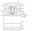
図1は、本実施形態にかかるトレンチゲート構造のMOSFETの斜視断面図である。この図は、MOSFETの1セル分を抽出したものに相当する。本図ではMOSFETの1セル分しか記載していないが、図1に示すMOSFETと同様の構造のMOSFETが複数列隣り合うように配置されている。また、図2(a)〜図2(d)は、図1のMOSFETの断面図である。図2(a)は、図1中のA−A線においてxz平面と平行に切断したときの断面、図2(b)は、図1中のB−B線においてxz平面と平行に切断したときの断面、図2(c)は、図1中のC−C線においてyz平面と平行に切断したときの断面、図2(d)は、図1中のD−D線においてyz平面と平行に切断したときの断面である。 FIG. 1 is a perspective sectional view of a MOSFET having a trench gate structure according to the present embodiment. This figure corresponds to the extracted one cell of the MOSFET. Although only one MOSFET cell is shown in the figure, MOSFETs having the same structure as the MOSFET shown in FIG. 1 are arranged so as to be adjacent to each other in a plurality of rows. 2A to 2D are cross-sectional views of the MOSFET of FIG. 2A is a cross-section taken along line AA in FIG. 1 in parallel with the xz plane, and FIG. 2B is cut in line parallel to the xz plane along line BB in FIG. 2C is a cross-sectional view taken along line CC in FIG. 1 and parallel to the yz plane. FIG. 2D is a cross-sectional view taken along line DD in FIG. It is a cross section when cut in parallel.
図1および図2(a)〜図2(d)に示すMOSFETは、SiCからなるn+型基板1が半導体基板として用いられている。n+型基板1は、リン等のn型不純物濃度が例えば1.0×10¹⁹/cm3とされ、厚さが300μm程度とされている。このn+型基板1の表面には、リン等のn型不純物濃度が例えば3.0〜7.0×1015/cm3で厚さ10〜15μm程度のSiCからなるn-型ドリフト層2が形成されている。このn-型ドリフト層2の不純物濃度は深さ方向において一定であっても良いが、濃度分布に傾斜を付け、n-型ドリフト層2のうちn+型基板1側の方がn+型基板1から離れる側よりも高濃度となるようにすると好ましい。例えば、n-型ドリフト層2のうちn+型基板1の表面から3〜5μm程度の部分の不純物濃度が2.0×1015/cm3程度他の部分よりも高くなるようにすると良い。このようにすると、n-型ドリフト層2の内部抵抗を低減できるため、オン抵抗を低減することが可能となる。
In the MOSFETs shown in FIGS. 1 and 2A to 2D, an n + type substrate 1 made of SiC is used as a semiconductor substrate. The n + -
このn-型ドリフト層2の表層部にはp型ベース領域3が形成されており、さらに、p型ベース領域3の上層部分にはn+型ソース領域4およびp+型コンタクト層5が形成されている。
A p-
p型ベース領域3は、ボロンもしくはアルミニウム等のp型不純物濃度が例えば5.0×10¹⁶〜2.0×10¹⁹/cm3、厚さ2.0μm程度で構成されている。n+型ソース領域4は、表層部におけるリン等のn型不純物濃度(表面濃度)が例えば1.0×1021/cm3、厚さ0.3μm程度で構成されている。p+型コンタクト層5は、例えば表層部におけるボロンもしくはアルミニウム等のp型不純物濃度(表面濃度)が例えば1.0×1021/cm3、厚さ0.3μm程度で構成されている。n+型ソース領域4は、後述するトレンチゲート構造の両側に配置されており、p+型コンタクト層5は、n+型ソース領域4を挟んでトレンチゲート構造と反対側に備えられている。
The p-
また、p型ベース領域3およびn+型ソース領域4を貫通してn-型ドリフト層2に達するように、例えば幅が1.4〜2.0μm、深さが2.0μm以上(例えば2.4μm)のトレンチ6が形成されている。このトレンチ6の側面と接するように上述したp型ベース領域3およびn+型ソース領域4が配置されている。
For example, the width is 1.4 to 2.0 μm and the depth is 2.0 μm or more (for example, 2 μm) so as to penetrate the p-
さらに、トレンチ6の内壁面はゲート酸化膜8にて覆われており、ゲート酸化膜8の表面に形成されたドープトPoly−Siにて構成されたゲート電極9により、トレンチ6内が埋め尽くされている。ゲート酸化膜8は、トレンチ6の内壁面を熱酸化することで形成されており、ゲート酸化膜8の厚みはトレンチ6の側面側と底部側共に100nm程度となっている。
Further, the inner wall surface of the
このようにして、トレンチゲート構造が構成されている。このトレンチゲート構造は、図1中のy方向を長手方向として延設されている。そして、複数のトレンチゲート構造が図1中のx方向に平行に並べられることでストライプ状とされている。また、上述したn+型ソース領域4およびp+型コンタクト層5もトレンチゲート構造の長手方向に沿って延設された構造とされている。
In this way, a trench gate structure is configured. This trench gate structure is extended with the y direction in FIG. 1 as the longitudinal direction. A plurality of trench gate structures are arranged in parallel in the x direction in FIG. 1 to form a stripe shape. Further, the n +
さらに、n-型ドリフト層2のうちp型ベース領域3よりも下方位置において、トレンチゲート構造に対して交差する方向に延設されたp型ディープ層10が形成されている。本実施形態の場合、p型ディープ層10は、トレンチゲート構造におけるトレンチ6の側面のうちチャネル領域が構成される部分に対する法線方向(図1中のx方向)、つまりトレンチ6の長手方向に対する垂直方向に延設され、それがトレンチ6の長手方向において複数本並べられて配置されている。このp型ディープ層10は、トレンチ6の底部よりも深く形成されており、n-型ドリフト層2の表面からの深さが例えば2.6〜3.0μm程度(p型ベース領域3の底部からの深さが例えば0.6〜1.0μm)とされている。また、p型ディープ層10は、p型ベース領域3と接することでp型ベース領域3と同電位に固定される。
Further, a p-type
図3は、トレンチゲート構造におけるゲート酸化膜8やゲート電極9などを省略して示したトレンチ6近傍の様子を示した部分斜視断面図である。図1や図2(a)〜図2(d)および図3に示されるように、本実施形態のp型ディープ層10は、第1領域に相当する下層領域10aと第2領域に相当する上層領域10bというステップ状に幅を異ならせた領域を備えている。つまり、本実施形態では、深さ方向においてp型ディープ層10の幅を変えており、上部の方が下部よりも幅が狭くなるようにしている。具体的には、下層領域10aではゲート酸化膜8内での電界集中を緩和して絶縁破壊を防止できるように耐圧を見込んで幅広に設定されており、上層領域10bではJFET領域の幅を広くしてJFET抵抗を低減できるように下層領域10aよりも幅狭に設定されている。これら下層領域10aおよび上層領域10bにより構成されるp型ディープ層10の不純物濃度は、ゲート酸化膜8内での電界集中を緩和して絶縁破壊を防止できるように、耐圧を見込んでボロンもしくはアルミニウム等のp型不純物濃度が決められており、例えば1.0×10¹⁷/cm3〜1.0×1019/cm3とされている。
FIG. 3 is a partial perspective sectional view showing the vicinity of the
本実施形態では、これら下層領域10aと上層領域10bとの境界の深さ、換言すれば上層領域10bの下面の深さは、トレンチ6よりも深くされており、トレンチ6の側面から底部まで上層領域10bが配置された構造とされている。このため、本実施形態の場合、ゲート電極9に対してゲート電圧を印加したときに、トレンチ6の側面にチャネルが形成されると、チャネルの幅はトレンチ6の最深部までn-型ドリフト層2のうち幅狭な上層領域10bの間に位置する部分となり、下層領域10aの間に位置する部分よりも広くなる。このため、下層領域10aよりも幅狭な上層領域10bを備えることにより、p型ディープ層10の幅をすべて下層領域10aと同じ幅にした場合と比較してJFET領域の幅を広くすることができ、JFET抵抗を低減することが可能となる。
In the present embodiment, the depth of the boundary between the
また、n+型ソース領域4およびp+型コンタクト層5の表面やゲート電極9の表面には、ソース電極11やゲート配線(図示せず)が形成されている。ソース電極11およびゲート配線は、複数の金属(例えばNi/Al等)にて構成されており、少なくともn型SiC(具体的にはn+型ソース領域4やnドープの場合のゲート電極9)と接触する部分はn型SiCとオーミック接触可能な金属で構成され、少なくともp型SiC(具体的にはp+型コンタクト層5やpドープの場合のゲート電極9)と接触する部分はp型SiCとオーミック接触可能な金属で構成されている。なお、これらソース電極11およびゲート配線は、層間絶縁膜12上に形成されることで電気的に絶縁されており、層間絶縁膜12に形成されたコンタクトホールを通じてソース電極11はn+型ソース領域4およびp+型コンタクト層5と電気的に接触させられ、ゲート配線はゲート電極9と電気的に接触させられている。
A
そして、n+型基板1の裏面側にはn+型基板1と電気的に接続されたドレイン電極13が形成されている。このような構造により、nチャネルタイプの反転型のトレンチゲート構造のMOSFETが構成されている。
Then, on the back side of the n + -type substrate 1 n + -
このような反転型のトレンチゲート構造のMOSFETは、以下のように動作する。まず、ゲート電極9にゲート電圧を印加する前の状態では、p型ベース領域3に反転層が形成されない。したがって、ドレイン電極13に正の電圧を加えたとしても、n型ソース領域4から電子はp型ベース領域3内に到達することはできず、ソース電極11とドレイン電極13との間に電流が流れない。
Such an inverted MOSFET having a trench gate structure operates as follows. First, the inversion layer is not formed in the p-
次に、オフ時(ゲート電圧=0V、ドレイン電圧=650V、ソース電圧=0V)には、ドレイン電極13に電圧を加えても逆バイアスになるため、p型ベース領域3とn-型ドリフト層2の間より空乏層が広がる。このとき、p型ベース領域3の濃度がn-型ドリフト層2より高いので、空乏層はほとんどn-型ドリフト層2側に広がる。例えば、p型ベース領域3の不純物濃度をn-型ドリフト層2の不純物濃度の10倍とした場合、p型ベース領域3側に約0.7μm伸び、n-型ドリフト層2側に約7.0μm伸びるが、p型ベース領域3の厚みを2.0μmと空乏層の伸び量よりも大きくしてあるため、パンチスルーしないようにできる。そして、ドレイン0Vの場合より空乏層が広がっているため、絶縁体として振舞う領域は更に広がっているので、ソース電極11とドレイン電極13との間に電流が流れない。
Next, when off (gate voltage = 0V, drain voltage = 650V, source voltage = 0V), a reverse bias is applied even if a voltage is applied to the
また、ゲート電圧が0Vになっているため、ドレイン−ゲート間にも電界がかかる。このため、ゲート酸化膜8の底部にも電界集中が発生し得る。しかしながら、トレンチ6よりも深いp型ディープ層10を備えた構造としているため、p型ディープ層10とn-型ドリフト層2とのPN接合部での空乏層がn-型ドリフト層2側に大きく伸びることになり、ドレイン電圧の影響による高電圧がゲート酸化膜8に入り込み難くなる。特に、耐圧を見込んでp型ディープ層10の下層領域10aの幅を設定してあるため、より高電圧がゲート酸化膜8に入り込まないようにすることが可能となる。これにより、ゲート酸化膜8内での電界集中、特にゲート酸化膜8のうちのトレンチ6の底部での電界集中を緩和することが可能となり、ゲート酸化膜8が破壊されることを防止することが可能となる。
In addition, since the gate voltage is 0 V, an electric field is also applied between the drain and the gate. For this reason, electric field concentration can also occur at the bottom of the
一方、オン時(ゲート電圧=20V、ドレイン電圧=1V、ソース電圧=0V)には、ゲート電極9にゲート電圧として20Vが印加されるため、p型ベース領域3のうちトレンチ6に接している表面にチャネルが形成される。このため、ソース電極11から注入された電子はn+型ソース領域4からp型ベース領域3に形成されたチャネルを通った後、n-型ドリフト層2に到達する。これにより、ソース電極11とドレイン電極13との間に電流を流すことができる。
On the other hand, when ON (gate voltage = 20 V, drain voltage = 1 V, source voltage = 0 V), 20 V is applied as the gate voltage to the
さらに、本実施形態では、p型ディープ層10の上層領域10bの幅を下層領域10aよりも狭くし、p型ディープ層10が浅くなるに連れて幅がステップ状に狭くなるようにしている。このため、オン時にゲート電極9にゲート電圧を印加してチャネルが形成されたときに、チャネルの幅を広くすることができる。すなわち、p型ディープ層10の上部周辺においては、チャネルの幅はn-型ドリフト層2のうち幅狭な上層領域10bの間に位置する部分となるため、n-型ドリフト層2のうち幅広な下層領域10aの間に位置する部分よりも広くなる。このため、チャネルの幅が広くなる。これにより、p型ディープ層10の幅をすべて下層領域10aと同じ幅にした場合と比較してJFET領域の幅を広くすることができ、JFET抵抗を低減することが可能となる。
Furthermore, in the present embodiment, the width of the
次に、図1に示すトレンチゲート構造のMOSFETの製造方法について説明する。図4〜図5は、図1に示すトレンチゲート構造のMOSFETの製造工程を示した断面図である。図4および図5中、左側に図1中のB−B線においてxz平面と平行に切断した断面図(図2(b)と対応する場所)を示してあり、右側に図1中のD−D線においてyz平面と平行に切断した断面図(図2(d)と対応する場所)を示してある。以下、これらの図を参照して説明する。 Next, a method for manufacturing the MOSFET having the trench gate structure shown in FIG. 1 will be described. 4 to 5 are cross-sectional views showing manufacturing steps of the MOSFET having the trench gate structure shown in FIG. 4 and 5, the left side shows a cross-sectional view taken along the line BB in FIG. 1 in parallel with the xz plane (the location corresponding to FIG. 2B), and the right side shows D in FIG. A cross-sectional view taken along line yz in parallel with the yz plane (a place corresponding to FIG. 2D) is shown. Hereinafter, description will be given with reference to these drawings.
〔図4(a)に示す工程〕
まず、リン等のn型不純物濃度が例えば1.0×10¹⁹/cm3で厚さ300μm程度のn+型基板1を用意する。このn+型基板1の表面にリン等のn型不純物濃度が例えば3.0〜7.0×1015/cm3で厚さ15μm程度のSiCからなるn-型ドリフト層2をエピタキシャル成長させる。
[Step shown in FIG. 4 (a)]
First, an n + -
〔図4(b)に示す工程〕
n-型ドリフト層2の表面にLTOなどで構成されるマスク20を形成したのち、フォトリソグラフィ工程を経て、p型ディープ層10のうちの下層領域10aの形成予定領域においてマスク20を開口させる。そして、マスク20上からp型不純物(例えばボロンやアルミニウム)のイオン注入を行う。例えばボロンもしくはアルミニウム濃度が1.0×10¹⁷/cm3〜1.0×1019/cm3となるようにイオン注入を行っている。その後、マスク20を除去する。
[Step shown in FIG. 4B]
After the
〔図4(c)に示す工程〕
n-型ドリフト層2の表面にLTOなどで構成されるマスク21を形成したのち、フォトリソグラフィ工程を経て、p型ディープ層10のうち上層領域10bの形成予定領域においてマスク21を開口させる。そして、マスク21上からp型不純物(例えばボロンやアルミニウム)のイオン注入を行う。このときのイオン注入の濃度については、図4(b)に示す工程と同様としている。この後、マスク21を除去したのち、注入されたイオンを活性化する。
[Step shown in FIG. 4 (c)]
After the
なお、ここでは下層領域10aを形成するためのp型不純物のイオン注入を行ったのちに、上層領域10bを形成するためのp型不純物のイオン注入を行うようにしたが、これらの順番を逆にしても良い。また、上層領域10bを形成するためのp型不純物のイオン注入を先に行う場合、そのときに使用したマスク21を用いて、下層領域10aを形成することでマスク共通化を図ることもできる。例えば、上層領域10bの形成後に、フッ酸などを用いたエッチングによってマスク21に形成されている開口部の開口端を後退させ、開口部の幅を下層領域10aと対応する幅に変更する。そして、開口部の幅を変更したマスク21を用いて、下層領域10aを形成するためのp型不純物のイオン注入を行う。このようにすれば、マスクの共通化を図ることができる。また、エッチングによりマスク21の開口端を後退させることによって下層領域10aと対応する開口部を形成しているため、上層領域10bと下層領域10aとをセルフアラインで形成でき、これらをマスクズレの影響無く形成することが可能となる。
Here, the p-type impurity ion implantation for forming the
〔図5(a)に示す工程〕
n-型ドリフト層2の表面に、ボロンもしくはアルミニウム等のp型不純物濃度が例えば5.0×10¹⁵〜5.0×10¹⁶/cm3、厚さ2.0μm程度となるp型不純物層をエピタキシャル成長させることにより、p型ベース領域3を形成する。
[Step shown in FIG. 5A]
A p-type impurity layer having a p-type impurity concentration such as boron or aluminum of about 5.0 × 10 15 to 5.0 × 10 16 / cm 3 and a thickness of about 2.0 μm is formed on the surface of the n − -
〔図5(b)に示す工程〕
続いて、p型ベース領域3の上に、例えばLTO等で構成されるマスク(図示せず)を成膜したのち、フォトリソグラフィ工程を経て、n+型ソース領域4の形成予定領域上においてマスクを開口させる。その後、n型不純物(例えば窒素)をイオン注入する。
[Step shown in FIG. 5B]
Subsequently, after forming a mask (not shown) made of, for example, LTO on the p-
さらに、先程使用したマスクを除去した後、再びマスク(図示せず)を成膜し、フォトリソグラフィ工程を経て、p+型コンタクト層5の形成予定領域上においてマスクを開口させる。その後、p型不純物(例えばボロンやアルミニウム)をイオン注入する。
Further, after removing the previously used mask, a mask (not shown) is formed again, and the mask is opened on a region where the p + -
そして、注入されたイオンを活性化することで、リン等のn型不純物濃度(表面濃度)が例えば1.0×10²¹/cm3、厚さ0.3μm程度のn+型ソース領域4を形成すると共に、ボロンもしくはアルミニウム等のp型不純物濃度(表面濃度)が例えば1.0×1021/cm3、厚さ0.3μm程度のp+型コンタクト層5を形成する。その後、マスクを除去する。
Then, by activating the implanted ions, the n + -
〔図5(c)に示す工程〕
p型ベース領域3、n+型ソース領域4およびp+型コンタクト層5の上に、図示しないエッチングマスクを成膜したのち、トレンチ6の形成予定領域においてエッチングマスクを開口させる。そして、エッチングマスクを用いた異方性エッチングを行ったのち、必要に応じて等方性エッチングや犠牲酸化工程を行うことで、トレンチ6を形成する。この後、エッチングマスクを除去する。
[Step shown in FIG. 5 (c)]
After forming an etching mask (not shown) on the p-
この後の工程に関しては、従来と同様であるため図示しないが、まず、ゲート酸化膜形成工程を行うことにより、トレンチ6内を含む基板表面全面にゲート酸化膜8を形成する。具体的には、ウェット雰囲気を用いたパイロジェニック法によるゲート酸化(熱酸化)によりゲート酸化膜8を形成する。続いて、ゲート酸化膜8の表面にn型不純物をドーピングしたポリシリコン層を例えば600℃の温度下で440nm程度成膜したのち、エッチバック工程等を行うことにより、トレンチ6内にゲート酸化膜8およびゲート電極9を残す。次に、層間絶縁膜12を成膜したのち、層間絶縁膜12をパターニングしてn+型ソース領域4やp+型コンタクト層5に繋がるコンタクトホールを形成すると共に、ゲート電極9に繋がるコンタクトホールを別断面に形成する。続いて、コンタクトホール内を埋め込むように電極材料を成膜したのち、これをパターニングすることでソース電極11やゲート配線を形成する。また、n+型基板1の裏面側にドレイン電極13を形成する。これにより、図1に示したMOSFETが完成する。
Since the subsequent steps are the same as those in the prior art and are not shown, first, a
以上説明したように、本実施形態のSiC半導体装置によれば、p型ディープ層10を深さが浅くなるほどステップ状に幅が狭くなる構造としている。具体的には、p型ディープ層10を下層領域10aと上層領域10bとにより構成し、上層領域10bを下層領域10aよりも幅が狭くなるようにしている。このため、オン時にゲート電極9にゲート電圧を印加してチャネルが形成されたときに、p型ディープ層10の上部周辺において、チャネルの幅を広くすることができ、p型ディープ層10の幅をすべて一定、つまり下層領域10aと同じ幅で一定とした場合と比較してJFET領域の幅を広くすることができ、JFET抵抗を低減することが可能となる。したがって、トレンチゲート構造を構成するトレンチ6に対して交差するようにp型ディープ層10を形成する場合において、隣り合うp型ディープ層10の間に構成されるJFET領域でのJFET抵抗を低減することができ、オン抵抗の低減を図ることが可能となる。
As described above, according to the SiC semiconductor device of the present embodiment, the p-type
(第2実施形態)
本発明の第2実施形態について説明する。本実施形態のSiC半導体装置は、第1実施形態に対してp型ディープ層10の構造を変更したものであり、基本構造に関しては第1実施形態と同様であるため、第1実施形態と異なっている部分に関してのみ説明する。
(Second Embodiment)
A second embodiment of the present invention will be described. The SiC semiconductor device according to the present embodiment is obtained by changing the structure of the p-type
図6は、本実施形態にかかるSiC半導体装置の斜視断面図である。また、図7(a)は図6のE−E線においてxz平面と平行に切断したときの断面図、図7(b)は、図6中のF−F線においてyz平面と平行に切断したときの断面図である。 FIG. 6 is a perspective sectional view of the SiC semiconductor device according to the present embodiment. 7A is a cross-sectional view taken along line EE in FIG. 6 in parallel with the xz plane, and FIG. 7B is cut in parallel with yz plane along line FF in FIG. It is sectional drawing when doing.
図6および図7(a)、(b)に示すように、本実施形態も、第1実施形態と同様に、p型ディープ層10の幅をp型ディープ層10の深さ方向において変えて、p型ディープ層10の上部の方が下部よりも幅が狭くなるようにしている。具体的には、p型ディープ層10の底部の幅については耐圧を考慮した幅とし、そこからp型ディープ層10の深さが浅くなるに連れて徐々に幅を縮小している。このような構成としても、第1実施形態のように、p型ディープ層10の底部の幅を広くして耐圧を確保しつつ、p型ディープ層10の上部の幅を狭くして、チャネルが広く形成されるようにすることが可能となり、電流経路を広げることが可能となる。したがって、隣り合うp型ディープ層10の間に構成されるJFET領域でのJFET抵抗を更に低減することができ、よりオン抵抗の低減を図ることが可能となる。
As shown in FIG. 6 and FIGS. 7A and 7B, the present embodiment also changes the width of the p-type
なお、本実施形態の構造のSiC半導体装置の製造方法は、基本的には第1実施形態と同様であり、図4(b)に示したp型ディープ層10の形成の際に、マスク21を用いて、斜めイオン注入によりp型不純物を注入し、p型ディープ層10が斜め方向に注入されるようにすれば良い。
The manufacturing method of the SiC semiconductor device having the structure of the present embodiment is basically the same as that of the first embodiment, and the
(第3実施形態)
本発明の第3実施形態について説明する。本実施形態のSiC半導体装置も、第1実施形態に対してよりオン抵抗を低減できる構造としたものであり、基本構造に関しては第1実施形態と同様であるため、第1実施形態と異なっている部分に関してのみ説明する。
(Third embodiment)
A third embodiment of the present invention will be described. The SiC semiconductor device of the present embodiment also has a structure that can reduce the on-resistance more than that of the first embodiment. The basic structure is the same as that of the first embodiment, so that it differs from the first embodiment. Only the parts that are present will be described.
図8は、本実施形態にかかるSiC半導体装置の斜視断面図である。また、図9(a)は図8のG−G線においてxz平面と平行に切断したときの断面図、図9(b)は、図8中のH−H線においてyz平面と平行に切断したときの断面図である。 FIG. 8 is a perspective sectional view of the SiC semiconductor device according to the present embodiment. 9A is a cross-sectional view taken along line GG in FIG. 8 in parallel with the xz plane, and FIG. 9B is cut in parallel with yz plane along line HH in FIG. It is sectional drawing when doing.
図8および図9(a)、(b)に示すように、本実施形態では、n-型ドリフト層2のうちの表面側、つまりn+型基板1とは反対側においてn型不純物濃度を高濃度とすることで電流拡散層2aを構成している。電流拡散層2aは、オン時に電流の流れる範囲をより広げるために設けたものであり、電流拡散層2aの不純物濃度は、例えば5.0×10¹⁶〜1.5×10¹⁷/cm3とされる。また、電流拡散層2aの厚さは例えば0.3〜0.7μmとされるが、本実施形態ではp型ディープ層10の上層領域10bの深さと等しくされている。
As shown in FIGS. 8 and 9A and 9B, in the present embodiment, the n-type impurity concentration is set on the surface side of the n − -
このような構造のSiC半導体装置には、オン時にゲート電極9にゲート電圧が印加されると、p型ベース領域3のうちトレンチ6に接している表面にチャネルが形成され、ソース電極11から注入された電子がn+型ソース領域4からp型ベース領域3に形成されたチャネルを通った後、n-型ドリフト層2の電流拡散層2aに到達する。これにより、低抵抗な電流拡散層2a内においてより電流の流れる範囲が広がり、トレンチゲート構造から離れた位置まで電流が流れるようになり、さらにオン抵抗を低減できる。
In the SiC semiconductor device having such a structure, when a gate voltage is applied to the
このように、p型ディープ層10を下層領域10aと上層領域10bにて構成する場合において、電流拡散層2aを備えた構造とすることもできる。これにより、よりオン抵抗の低減を図ることが可能となる。
Thus, in the case where the p-type
次に、本実施形態の構造のSiC半導体装置の製造方法について説明する。図10および図11は、本実施形態にかかるSiC半導体装置の製造工程を示した断面図である。図10および図11中、左側に図8中のG−G線においてxz平面と平行に切断した断面図(図9(a)と対応する場所)を示してあり、右側に図8中のH−H線においてyz平面と平行に切断した断面図(図9(b)と対応する場所)を示してある。これらの図を参照して、本実施形態のSiC半導体装置の製造方法について説明する。 Next, a manufacturing method of the SiC semiconductor device having the structure of the present embodiment will be described. 10 and 11 are cross-sectional views showing the manufacturing process of the SiC semiconductor device according to the present embodiment. 10 and 11, the left side shows a cross-sectional view taken along the line GG in FIG. 8 in parallel with the xz plane (the location corresponding to FIG. 9A), and the right side shows H in FIG. A cross-sectional view taken along line yz in parallel with the yz plane (a place corresponding to FIG. 9B) is shown. With reference to these drawings, a method of manufacturing the SiC semiconductor device of this embodiment will be described.
まず、図10(a)に示す工程でn+型基板1の表面にn-型ドリフト層2をエピタキシャル成長させる。このとき、n-型ドリフト層2のうち電流拡散層2aを除く部分を形成する(第1工程)。その後、図10(b)に示す工程でn-型ドリフト層2の表面にマスク23を配置したのち、p型ディープ層10のうちの下層領域10aの形成予定領域においてマスク20を開口させたのち、マスク20上からp型不純物(例えばボロンやアルミニウム)のイオン注入を行う。
First, the n −
続いて、マスク20を除去した後、図10(c)に示す工程において、例えばn型不純物濃度が5.0×10¹⁶〜1.5×10¹⁷/cm3、厚さが0.3〜0.7μmの電流拡散層2aを形成する(第2工程)。この後、電流拡散層2aの表面にマスク21を形成したのち、p型ディープ層10のうち上層領域10bの形成予定領域においてマスク21を開口させる。そして、マスク21上からp型不純物(例えばボロンやアルミニウム)のイオン注入を行い、さらにマスク21を除去したのち、注入されたイオンを活性化する。このようにして、電流拡散層2aが部分的にp型に補償されることで上層領域10bが形成され、先に形成されていた下層領域10aと繋がってp型ディープ層10が構成される。
Subsequently, after removing the
この後、図11(a)〜(c)に示す工程において、図5(a)〜(c)に示す工程と同様の工程を行い、図8に示す本実施形態のSiC半導体装置が完成する。 Thereafter, in the steps shown in FIGS. 11A to 11C, the same steps as those shown in FIGS. 5A to 5C are performed, and the SiC semiconductor device of the present embodiment shown in FIG. 8 is completed. .
(第4実施形態)
本発明の第4実施形態について説明する。本実施形態のSiC半導体装置は、第3実施形態に対してよりゲート酸化膜8での電界集中を緩和できる構造としたものであり、基本構造に関しては第3実施形態と同様であるため、第3実施形態と異なっている部分に関してのみ説明する。
(Fourth embodiment)
A fourth embodiment of the present invention will be described. The SiC semiconductor device of the present embodiment has a structure that can reduce the electric field concentration in the
図12は、本実施形態にかかるSiC半導体装置の斜視断面図である。また、図13(a)は図12のI−I線においてxz平面と平行に切断したときの断面図、図13(b)は、図12中のJ−J線においてyz平面と平行に切断したときの断面図である。 FIG. 12 is a perspective sectional view of the SiC semiconductor device according to the present embodiment. 13A is a cross-sectional view taken along the line I-I in FIG. 12 parallel to the xz plane, and FIG. 13B is a line cut along the line JJ in FIG. 12 parallel to the yz plane. It is sectional drawing when doing.
図12および図13(a)、(b)に示すように、本実施形態では、第3実施形態と同様にn-型ドリフト層2のうちの表面側に電流拡散層2aを形成しつつ、さらにトレンチ6が電流拡散層2aを突き抜け、トレンチ6の底部が電流拡散層2aよりも深い位置まで形成されるようにしている。
As shown in FIG. 12 and FIGS. 13A and 13B, in the present embodiment, the
このような構造のSiC半導体装置では、トレンチゲート構造が電流拡散層2aよりも深い位置まで形成されることで、第3実施形態と比較して、ゲート酸化膜8への電界集中を緩和することが可能となる。具体的には、電流拡散層2aは、n-型ドリフト層2の中でも比較的不純物濃度を高くしたものであり、不純物濃度が高い箇所では電界集中が発生し易い。このため、トレンチゲート構造の深さを電流拡散層2aよりも深い位置、つまりn-型ドリフト層2における比較的不純物濃度が低い箇所まで深くすることで、電界集中を緩和することが可能となる。これにより、電界集中によってゲート酸化膜8が破壊されることをより防止することが可能となる。
In the SiC semiconductor device having such a structure, the trench gate structure is formed to a position deeper than the
なお、このような構造のSiC半導体装置の製造方法についてはほぼ第3実施形態と同様であり、第3実施形態で説明した図11(c)の工程でのトレンチ6の形成深さを変更し、トレンチ6が電流拡散層2aよりも深くなるようにするだけで良い。勿論、トレンチ6の形成深さを変更するのではなく、第3実施形態と比較して電流拡散層2aの厚みを薄く設定しておくことでトレンチ6が電流拡散層2aよりも深くなるようにしても良い。
The manufacturing method of the SiC semiconductor device having such a structure is almost the same as that of the third embodiment, and the formation depth of the
(第5実施形態)
本発明の第5実施形態について説明する。本実施形態のSiC半導体装置は、第3実施形態に対して電流拡散層2aの濃度を変更したものであり、基本構造に関しては第3実施形態と同様であるため、第3実施形態と異なっている部分に関してのみ説明する。
(Fifth embodiment)
A fifth embodiment of the present invention will be described. The SiC semiconductor device of the present embodiment is obtained by changing the concentration of the
図14は、本実施形態にかかるSiC半導体装置の斜視断面図である。また、図15(a)は図14のK−K線においてxz平面と平行に切断したときの断面図、図15(b)は、図14中のL−L線においてyz平面と平行に切断したときの断面図である。 FIG. 14 is a perspective sectional view of the SiC semiconductor device according to the present embodiment. 15A is a cross-sectional view taken along the line KK in FIG. 14 parallel to the xz plane, and FIG. 15B is a line cut along the line LL in FIG. 14 parallel to the yz plane. It is sectional drawing when doing.
図14および図15(a)、(b)に示すように、本実施形態では、第3実施形態と同様にn-型ドリフト層2のうちの表面側に電流拡散層2aを形成しているが、電流拡散層2aに濃度分布を設け、電流拡散層2aのn型不純物濃度が下部ほど薄く、上部ほど濃くなるようにしている。
As shown in FIGS. 14, 15A, and 15B, in the present embodiment, the
このような構造のSiC半導体装置では、電流拡散層2aの下部のn型不純物濃度が薄くされていることから、トレンチ6の底部が電流拡散層2aのうち比較的不純物濃度が低くされている箇所に位置することになる。このため、ゲート酸化膜8への電界集中を緩和することが可能となる。その一方で、電流拡散層2aのうちの上部についてはn型不純物濃度が濃くされていることから、低抵抗な電流拡散層2a内においてより電流の流れる範囲を広げることができるため、オン抵抗の低減も図れる。したがって、電界集中によるゲート酸化膜8の破壊防止と、オン抵抗の低減の両立を図ることが可能となる。
In the SiC semiconductor device having such a structure, since the n-type impurity concentration in the lower portion of the
なお、このような構造のSiC半導体装置の製造方法についてはほぼ第3実施形態と同様であり、第3実施形態で説明した図10(c)の工程での電流拡散層2aを形成するためのエピタキシャル成長をn型不純物のドーピング量が徐々に増加するように変化させながら行うようにすれば良い。
The manufacturing method of the SiC semiconductor device having such a structure is substantially the same as that of the third embodiment, and is for forming the
また、このように電流拡散層2aのn型不純物濃度について深さ方向に濃度分布をつける構造は、上記した第4実施形態に対して適用することもできる。
In addition, the structure in which the concentration distribution in the depth direction is applied to the n-type impurity concentration of the
(他の実施形態)
(1)上記各実施形態では、p型ディープ層10の幅を上部が狭く、下部が広くする構造の一例を挙げ、第1、第3実施形態では、p型ディープ層10が浅くなるに連れて幅がステップ状に狭くなる形態、第2実施形態では、p型ディープ層10が浅くなるに連れて幅が徐々に狭くなる形態を説明した。しかしながら、これらは一例を示したに過ぎず、他の構造であっても、p型ディープ層10の幅を上部が狭く、下部が広くされていれば、JFET抵抗の低減によるオン抵抗低減の効果を得ることができる。勿論、第1、第3実施形態で説明したような下層領域10aと上層領域10bを有したステップ状にp型ディープ層10の幅を変化させる構造についても、ステップ数をより多くの多段とすることも可能である。
(Other embodiments)
(1) In each of the above embodiments, an example of a structure in which the upper part of the p-type
(2)上記各実施形態では、p型ディープ層10をx方向に延設した場合について説明したが、各p型ディープ層10をトレンチ6の長手方向に対して斜め方向に交差する形状にしたり、X方向において複数に分割した形状としても良い。p型ディープ層10をトレンチ6の長手方向に対して斜め方向に交差する構造とする場合、等電位分布の偏りなどを抑制するために、トレンチ6の長手方向に対する垂直方向に伸びる線を対称線として、p型ディープ層10を線対称のレイアウトにするのが好ましい。
(2) In each of the above embodiments, the case where the p-type
(3)上記各実施形態では、第1導電型をn型、第2導電型をp型としたnチャネルタイプのMOSFETを例に挙げて説明したが、各構成要素の導電型を反転させたpチャネルタイプのMOSFETに対しても本発明を適用することができる。また、上記説明では、トレンチゲート構造のMOSFETを例に挙げて説明したが、同様のトレンチゲート構造のIGBTに対しても本発明を適用することができる。IGBTは、上記各実施形態に対して基板1の導電型をn型からp型に変更するだけであり、その他の構造や製造方法に関しては上記各実施形態と同様である。
(3) In each of the above embodiments, an n-channel type MOSFET in which the first conductivity type is n-type and the second conductivity type is p-type has been described as an example. However, the conductivity type of each component is inverted. The present invention can also be applied to a p-channel type MOSFET. In the above description, a MOSFET having a trench gate structure has been described as an example. However, the present invention can also be applied to an IGBT having a similar trench gate structure. The IGBT only changes the conductivity type of the
(4)上記各実施形態では、ゲート絶縁膜として熱酸化によるゲート酸化膜8を例に挙げて説明したが熱酸化によらない酸化膜もしくは窒化膜などを含むものであっても構わない。
(4) In each of the above embodiments, the
(5)上記第3実施形態では、SiC半導体装置の製造方法として、図10および図11に示す工程を行う場合について説明したが、基本的には第1実施形態と同様の工程を行い、図4(a)に示したn-型ドリフト層2の形成工程の最終段階で、成長時にドーピングされる不純物濃度を高くすることで電流拡散層2aを形成するようにしても良い。この場合でも、図4(c)に示した上層領域10bを形成する際にイオン注入されるp型不純物濃度を第1実施形態と比較して高く設定しておくことで、図8に示した構造のSiC半導体装置を製造することができる。
(5) In the third embodiment, the case where the steps shown in FIGS. 10 and 11 are performed as the method of manufacturing the SiC semiconductor device has been described, but basically the same steps as those in the first embodiment are performed. At the final stage of the formation process of the n −
また、上記第3実施形態では、第1実施形態のようにp型ディープ層10を下層領域10aと上層領域10bとによって構成する構造に対して電流拡散層2aを形成する場合について説明したが、第2実施形態の構造に対して電流拡散層2aを形成することもできる。
Moreover, although the said 3rd Embodiment demonstrated the case where the electric current spreading |
1 n+型基板
2 n-型ドリフト層
3 p型ベース領域
4 n+型ソース領域
5 p+型コンタクト層
6 トレンチ
8 ゲート酸化膜
9 ゲート電極
10 p型ディープ層
10a 下層領域
10b 上層領域
11 ソース電極
12 層間絶縁膜
13 ドレイン電極
20、21 マスク
1 n + type substrate 2 n − type drift layer 3 p type base region 4 n + type source region 5 p +
Claims (10)
前記基板(1)の上に形成され、前記基板(1)よりも低不純物濃度とされた第1導電型の炭化珪素からなるドリフト層(2)と、
前記ドリフト層(2)の上に形成された第2導電型の炭化珪素からなるベース領域(3)と、
前記ベース領域(3)の上層部に形成され、前記ドリフト層(2)よりも高濃度の第1導電型の炭化珪素にて構成されたソース領域(4)と、
前記ベース領域(3)の上層部に形成され、前記ベース層(3)よりも高濃度の第2導電型の炭化珪素にて構成されたコンタクト領域(5)と、
前記ソース領域(4)の表面から前記ベース領域(3)よりも深くまで形成され、一方向を長手方向として形成されたトレンチ(6)と、
前記トレンチ(6)の内壁面に形成されたゲート絶縁膜(8)と、
前記トレンチ(6)内において、前記ゲート絶縁膜(8)の上に形成されたゲート電極(9)と、
前記ソース領域(4)および前記ベース領域(3)に電気的に接続されたソース電極(11)と、
前記基板(1)の裏面側に形成されたドレイン電極(13)とを備え、
前記ゲート電極(9)への印加電圧を制御することで前記トレンチ(6)の側面に位置する前記ベース領域(3)の表面部に反転型のチャネル領域を形成し、前記ソース領域(4)および前記ドリフト層(2)を介して、前記ソース電極(11)および前記ドレイン電極(13)の間に電流を流す反転型の半導体スイッチング素子を備えた炭化珪素半導体装置であって、
前記ベース領域(3)の下方に配置されると共に前記トレンチ(6)よりも深い位置まで形成され、前記トレンチ(6)の長手方向と交差する複数の第2導電型のディープ層(10)を有し、
前記ディープ層(10)は、該ディープ層(10)の上部の方が該ディープ層(10)の下部よりも幅が狭くされていることを特徴とする炭化珪素半導体装置。 A first or second conductivity type substrate (1) made of silicon carbide;
A drift layer (2) made of silicon carbide of the first conductivity type formed on the substrate (1) and having a lower impurity concentration than the substrate (1);
A base region (3) made of silicon carbide of the second conductivity type formed on the drift layer (2);
A source region (4) formed in an upper layer portion of the base region (3) and made of silicon carbide of the first conductivity type having a higher concentration than the drift layer (2);
A contact region (5) formed in an upper layer portion of the base region (3) and made of silicon carbide of the second conductivity type having a higher concentration than the base layer (3);
A trench (6) formed from the surface of the source region (4) to a depth deeper than the base region (3) and having one direction as a longitudinal direction;
A gate insulating film (8) formed on the inner wall surface of the trench (6);
A gate electrode (9) formed on the gate insulating film (8) in the trench (6);
A source electrode (11) electrically connected to the source region (4) and the base region (3);
A drain electrode (13) formed on the back side of the substrate (1),
By controlling the voltage applied to the gate electrode (9), an inversion channel region is formed on the surface of the base region (3) located on the side surface of the trench (6), and the source region (4) And a silicon carbide semiconductor device comprising an inversion type semiconductor switching element for passing a current between the source electrode (11) and the drain electrode (13) via the drift layer (2),
A plurality of second conductivity type deep layers (10) disposed below the base region (3) and formed deeper than the trench (6) and intersecting the longitudinal direction of the trench (6). Have
The deep layer (10) is a silicon carbide semiconductor device characterized in that the upper part of the deep layer (10) is narrower than the lower part of the deep layer (10).
前記ドリフト層(2)の表面にマスク(20、21)を配置した後、該マスク(20、21)を用いたイオン注入を行うことにより、前記ドリフト層(2)の表層部に第2導電型のディープ層(10)を形成する工程と、
前記ディープ層(10)および前記ドリフト層(2)の上に第2導電型の炭化珪素からなるベース領域(3)を形成する工程と、
前記ベース領域(3)内における該ベース領域(3)の表層部に第1導電型不純物をイオン注入することにより、前記ドリフト層(2)よりも高濃度の第1導電型の炭化珪素にて構成されたソース領域(4)を形成する工程と、
前記ベース領域(3)内における該ベース領域(3)の表層部に第2導電型不純物をイオン注入することにより、前記ベース領域(3)よりも高濃度の第2導電型の炭化珪素にて構成されたコンタクト領域(5)を形成する工程と、
前記ソース領域(4)の表面から前記ベース領域(3)を貫通して前記ドリフト層(2)に達し、かつ、前記ディープ層(10)よりも浅く、一方向を長手方向とするトレンチ(6)を形成する工程と、
前記トレンチ(6)の表面にゲート絶縁膜(8)を形成する工程と、
前記トレンチ(6)内において、前記ゲート絶縁膜(8)の上にゲート電極(9)を形成する工程と、
前記ソース領域(4)および前記コンタクト領域(5)を介して前記ベース領域(3)に電気的に接続されるソース電極(11)を形成する工程と、
前記基板(1)の裏面側にドレイン電極(13)を形成する工程と、を含み、
前記ディープ層(10)を形成する工程では、前記ベース領域(3)の下方に配置されると共に前記トレンチ(6)よりも深い位置まで、かつ、前記トレンチ(6)の長手方向と交差し、上部の方が下部よりも幅が狭くなるように前記ディープ層(10)を形成することを特徴とする炭化珪素半導体装置の製造方法。 Forming a drift layer (2) made of silicon carbide of the first conductivity type having a lower impurity concentration than the substrate (1) on the first or second conductivity type substrate (1) made of silicon carbide; When,
After disposing a mask (20, 21) on the surface of the drift layer (2), ion implantation using the mask (20, 21) is performed, so that a second conductive layer is formed in the surface layer portion of the drift layer (2). Forming a deep layer (10) of the mold;
Forming a base region (3) made of silicon carbide of the second conductivity type on the deep layer (10) and the drift layer (2);
By ion-implanting the first conductivity type impurity into the surface layer portion of the base region (3) in the base region (3), the first conductivity type silicon carbide having a higher concentration than the drift layer (2) is obtained. Forming a configured source region (4);
By ion-implanting the second conductivity type impurity into the surface layer portion of the base region (3) in the base region (3), the second conductivity type silicon carbide having a higher concentration than the base region (3) is obtained. Forming a configured contact region (5);
A trench (6) extending from the surface of the source region (4) through the base region (3) to the drift layer (2) and shallower than the deep layer (10) and having one direction as a longitudinal direction. )
Forming a gate insulating film (8) on the surface of the trench (6);
Forming a gate electrode (9) on the gate insulating film (8) in the trench (6);
Forming a source electrode (11) electrically connected to the base region (3) via the source region (4) and the contact region (5);
Forming a drain electrode (13) on the back side of the substrate (1),
In the step of forming the deep layer (10), it is disposed below the base region (3) and deeper than the trench (6), and intersects the longitudinal direction of the trench (6). The method of manufacturing a silicon carbide semiconductor device, wherein the deep layer (10) is formed so that the width of the upper part is narrower than that of the lower part.
前記ドリフト層(2)の表面にマスク(20)を形成したのち、該マスク(20)を部分的に開口させ、該マスク(20)の上方から第2導電型不純物をイオン注入することで前記ディープ層(10)のうちの第1領域(10a)を形成する工程と、
前記ドリフト層(2)の表面にマスク(21)を形成したのち、該マスク(21)を部分的に開口させ、該マスク(21)の上方から第2導電型不純物をイオン注入することで前記ディープ層(10)のうちの前記第1領域(10a)の上方に位置する第2領域(10b)を前記第1領域(10a)よりも狭い幅で形成する工程とを含んでいることを特徴とする請求項7に記載の炭化珪素半導体装置の製造方法。 In the step of forming the deep layer (10),
After the mask (20) is formed on the surface of the drift layer (2), the mask (20) is partially opened, and second conductivity type impurities are ion-implanted from above the mask (20). Forming a first region (10a) of the deep layer (10);
After the mask (21) is formed on the surface of the drift layer (2), the mask (21) is partially opened, and second conductivity type impurities are ion-implanted from above the mask (21). Forming a second region (10b) located above the first region (10a) in the deep layer (10) with a width narrower than that of the first region (10a). A method for manufacturing a silicon carbide semiconductor device according to claim 7.
前記ドリフト層(2)を形成する工程では、該ドリフト層(2)のうち前記電流拡散層(2a)を除く部分を形成する第1工程と、前記電流拡散層(2a)を形成する第2工程とを含み、
前記第1領域(10a)を形成する工程は、前記第1工程を行ったのち、前記第2工程の前に行われることで、前記ドリフト層(2)のうち前記電流拡散層(2a)を除く部分に対して前記第1領域(10a)を形成する工程であり、
前記第2領域(10b)を形成する工程は、前記第2工程を行ったのちに行われることで、前記電流拡散層(2a)に対して前記第2領域(10b)を形成する工程であることを特徴とする請求項8に記載の炭化珪素半導体装置の製造方法。 More than the portion of the drift layer (2) located below the deep layer (10) in the portion disposed between the adjacent deep layers (10). Forming a high-concentration first conductive type current diffusion layer (2a);
In the step of forming the drift layer (2), a first step of forming the drift layer (2) excluding the current diffusion layer (2a) and a second step of forming the current diffusion layer (2a). Process,
The step of forming the first region (10a) is performed after the first step and before the second step, so that the current diffusion layer (2a) of the drift layer (2) is formed. Forming the first region (10a) with respect to a portion to be removed;
The step of forming the second region (10b) is a step of forming the second region (10b) with respect to the current diffusion layer (2a) by being performed after the second step. A method for manufacturing a silicon carbide semiconductor device according to claim 8.
Priority Applications (5)
| Application Number | Priority Date | Filing Date | Title |
|---|---|---|---|
| JP2011027995A JP2012169384A (en) | 2011-02-11 | 2011-02-11 | Silicon carbide semiconductor device and method of manufacturing the same |
| US13/994,855 US20140175459A1 (en) | 2011-02-11 | 2012-02-06 | Silicon carbide semiconductor device and method for manufacturing the same |
| DE112012000748.4T DE112012000748T5 (en) | 2011-02-11 | 2012-02-06 | Silicon carbide semiconductor device and method of manufacturing the same |
| PCT/JP2012/000769 WO2012108166A1 (en) | 2011-02-11 | 2012-02-06 | Silicon carbide semiconductor device and method for manufacturing the same |
| CN2012800083291A CN103348478A (en) | 2011-02-11 | 2012-02-06 | Silicon carbide semiconductor device and method for manufacturing the same |
Applications Claiming Priority (1)
| Application Number | Priority Date | Filing Date | Title |
|---|---|---|---|
| JP2011027995A JP2012169384A (en) | 2011-02-11 | 2011-02-11 | Silicon carbide semiconductor device and method of manufacturing the same |
Publications (1)
| Publication Number | Publication Date |
|---|---|
| JP2012169384A true JP2012169384A (en) | 2012-09-06 |
Family
ID=45774298
Family Applications (1)
| Application Number | Title | Priority Date | Filing Date |
|---|---|---|---|
| JP2011027995A Pending JP2012169384A (en) | 2011-02-11 | 2011-02-11 | Silicon carbide semiconductor device and method of manufacturing the same |
Country Status (5)
| Country | Link |
|---|---|
| US (1) | US20140175459A1 (en) |
| JP (1) | JP2012169384A (en) |
| CN (1) | CN103348478A (en) |
| DE (1) | DE112012000748T5 (en) |
| WO (1) | WO2012108166A1 (en) |
Cited By (20)
| Publication number | Priority date | Publication date | Assignee | Title |
|---|---|---|---|---|
| JP2014160720A (en) * | 2013-02-19 | 2014-09-04 | Sanken Electric Co Ltd | Semiconductor device |
| JP2015133447A (en) * | 2014-01-15 | 2015-07-23 | 株式会社豊田中央研究所 | Semiconductor device |
| WO2016002766A1 (en) * | 2014-06-30 | 2016-01-07 | 国立研究開発法人産業技術総合研究所 | Silicon carbide semiconductor device and production method for same |
| WO2016042738A1 (en) * | 2014-09-16 | 2016-03-24 | 株式会社デンソー | Silicon carbide semiconductor device and method for manufacturing same |
| JP2016066780A (en) * | 2014-09-16 | 2016-04-28 | 株式会社デンソー | Silicon carbide semiconductor device and manufacturing method of the same |
| WO2017064949A1 (en) * | 2015-10-16 | 2017-04-20 | 富士電機株式会社 | Semiconductor device and method for manufacturing semiconductor device |
| JP2017092368A (en) * | 2015-11-16 | 2017-05-25 | 富士電機株式会社 | Semiconductor device and semiconductor device manufacturing method |
| JP2018046254A (en) * | 2016-09-16 | 2018-03-22 | トヨタ自動車株式会社 | Switching element |
| JP2018060943A (en) * | 2016-10-06 | 2018-04-12 | トヨタ自動車株式会社 | Switching element |
| JP2018098324A (en) * | 2016-12-12 | 2018-06-21 | 株式会社デンソー | Silicon carbide semiconductor device and manufacturing method of the same |
| KR101875638B1 (en) * | 2016-10-14 | 2018-07-06 | 현대자동차 주식회사 | Semiconductor device and method manufacturing the same |
| US10236339B2 (en) | 2016-09-21 | 2019-03-19 | Kabushiki Kaisha Toshiba | Semiconductor device |
| JP2020109808A (en) * | 2019-01-07 | 2020-07-16 | 株式会社デンソー | Semiconductor device |
| JP2020109809A (en) * | 2019-01-07 | 2020-07-16 | 株式会社デンソー | Semiconductor device |
| JP2020109810A (en) * | 2019-01-07 | 2020-07-16 | 株式会社デンソー | Semiconductor device |
| JP2020109811A (en) * | 2019-01-07 | 2020-07-16 | 株式会社デンソー | Semiconductor device |
| WO2021100206A1 (en) * | 2019-11-22 | 2021-05-27 | 株式会社デンソー | Switching element |
| WO2021215445A1 (en) * | 2020-04-22 | 2021-10-28 | 株式会社デンソー | Semiconductor device |
| WO2022190456A1 (en) * | 2021-03-11 | 2022-09-15 | 株式会社デンソー | Field-effect transistor, and method for manufacturing same |
| WO2022190444A1 (en) * | 2021-03-11 | 2022-09-15 | 株式会社デンソー | Field effect transistor |
Families Citing this family (25)
| Publication number | Priority date | Publication date | Assignee | Title |
|---|---|---|---|---|
| DE112013006639T5 (en) * | 2013-02-25 | 2015-10-29 | Hitachi, Ltd. | Semiconductor device, semiconductor device driving device, and power conversion device |
| DE112013006638T5 (en) * | 2013-02-25 | 2015-10-29 | Hitachi, Ltd. | Semiconductor device, semiconductor device driving device, and power conversion device |
| JP6077380B2 (en) * | 2013-04-24 | 2017-02-08 | トヨタ自動車株式会社 | Semiconductor device |
| US9024328B2 (en) | 2013-07-02 | 2015-05-05 | General Electric Company | Metal-oxide-semiconductor (MOS) devices with increased channel periphery and methods of manufacture |
| US9748341B2 (en) * | 2013-07-02 | 2017-08-29 | General Electric Company | Metal-oxide-semiconductor (MOS) devices with increased channel periphery |
| JP6135364B2 (en) * | 2013-07-26 | 2017-05-31 | 住友電気工業株式会社 | Silicon carbide semiconductor device and manufacturing method thereof |
| JP2015060859A (en) * | 2013-09-17 | 2015-03-30 | 住友電気工業株式会社 | Silicon carbide semiconductor device and method of manufacturing the same |
| JP6237408B2 (en) * | 2014-03-28 | 2017-11-29 | 住友電気工業株式会社 | Silicon carbide semiconductor device and manufacturing method thereof |
| JP6420175B2 (en) * | 2014-05-22 | 2018-11-07 | ルネサスエレクトロニクス株式会社 | Semiconductor device |
| JP6300638B2 (en) * | 2014-05-26 | 2018-03-28 | ルネサスエレクトロニクス株式会社 | Semiconductor device |
| KR101988202B1 (en) * | 2016-08-10 | 2019-06-11 | 닛산 지도우샤 가부시키가이샤 | Semiconductor device |
| CN106784011A (en) * | 2017-03-23 | 2017-05-31 | 北京世纪金光半导体有限公司 | Carborundum UMOSFET device structure cells with surge voltage from pressing down and from overvoltage protection |
| US10468509B2 (en) * | 2017-06-07 | 2019-11-05 | Fuji Electric Co., Ltd. | Semiconductor device and method of manufacturing semiconductor device |
| JP6729523B2 (en) * | 2017-08-31 | 2020-07-22 | 株式会社デンソー | Silicon carbide semiconductor device and manufacturing method thereof |
| JP6870547B2 (en) * | 2017-09-18 | 2021-05-12 | 株式会社デンソー | Semiconductor devices and their manufacturing methods |
| US10600649B2 (en) * | 2017-09-21 | 2020-03-24 | General Electric Company | Systems and method for charge balanced semiconductor power devices with fast switching capability |
| KR102335490B1 (en) * | 2017-12-14 | 2021-12-03 | 현대자동차 주식회사 | Semiconductor device and method manufacturing the same |
| JP6910944B2 (en) * | 2017-12-27 | 2021-07-28 | ルネサスエレクトロニクス株式会社 | Semiconductor device |
| CN109979935A (en) * | 2017-12-28 | 2019-07-05 | 富士电机株式会社 | The manufacturing method of semiconductor device and semiconductor device |
| JP7180402B2 (en) * | 2019-01-21 | 2022-11-30 | 株式会社デンソー | semiconductor equipment |
| JP7140148B2 (en) * | 2019-02-27 | 2022-09-21 | 株式会社デンソー | Silicon carbide semiconductor device and manufacturing method thereof |
| CN111129109A (en) * | 2019-12-04 | 2020-05-08 | 深圳第三代半导体研究院 | Silicon carbide high-voltage MOS device and manufacturing method thereof |
| JP7425943B2 (en) * | 2019-12-12 | 2024-02-01 | 株式会社デンソー | silicon carbide semiconductor device |
| CN112992682A (en) * | 2019-12-13 | 2021-06-18 | 华润微电子(重庆)有限公司 | Groove type field effect transistor structure and preparation method thereof |
| GB2592928A (en) * | 2020-03-10 | 2021-09-15 | Mqsemi Ag | Insulated gate switched transistor |
Citations (2)
| Publication number | Priority date | Publication date | Assignee | Title |
|---|---|---|---|---|
| JP2008108962A (en) * | 2006-10-26 | 2008-05-08 | Toshiba Corp | Semiconductor device |
| JP2009259896A (en) * | 2008-04-14 | 2009-11-05 | Denso Corp | Method for manufacturing silicon carbide semiconductor device |
Family Cites Families (5)
| Publication number | Priority date | Publication date | Assignee | Title |
|---|---|---|---|---|
| JP2004047967A (en) * | 2002-05-22 | 2004-02-12 | Denso Corp | Semiconductor device and method for manufacturing same |
| JP2007027193A (en) * | 2005-07-12 | 2007-02-01 | Renesas Technology Corp | Semiconductor device, its manufacturing method and non-insulated dc/dc converter |
| EP2091083A3 (en) | 2008-02-13 | 2009-10-14 | Denso Corporation | Silicon carbide semiconductor device including a deep layer |
| JP4793390B2 (en) | 2008-02-13 | 2011-10-12 | 株式会社デンソー | Silicon carbide semiconductor device and manufacturing method thereof |
| WO2009110229A1 (en) * | 2008-03-07 | 2009-09-11 | 三菱電機株式会社 | Silicon carbide semiconductor device and manufacturing method thereof |
-
2011
- 2011-02-11 JP JP2011027995A patent/JP2012169384A/en active Pending
-
2012
- 2012-02-06 CN CN2012800083291A patent/CN103348478A/en active Pending
- 2012-02-06 WO PCT/JP2012/000769 patent/WO2012108166A1/en active Application Filing
- 2012-02-06 DE DE112012000748.4T patent/DE112012000748T5/en not_active Withdrawn
- 2012-02-06 US US13/994,855 patent/US20140175459A1/en not_active Abandoned
Patent Citations (2)
| Publication number | Priority date | Publication date | Assignee | Title |
|---|---|---|---|---|
| JP2008108962A (en) * | 2006-10-26 | 2008-05-08 | Toshiba Corp | Semiconductor device |
| JP2009259896A (en) * | 2008-04-14 | 2009-11-05 | Denso Corp | Method for manufacturing silicon carbide semiconductor device |
Cited By (33)
| Publication number | Priority date | Publication date | Assignee | Title |
|---|---|---|---|---|
| JP2014160720A (en) * | 2013-02-19 | 2014-09-04 | Sanken Electric Co Ltd | Semiconductor device |
| JP2015133447A (en) * | 2014-01-15 | 2015-07-23 | 株式会社豊田中央研究所 | Semiconductor device |
| JPWO2016002766A1 (en) * | 2014-06-30 | 2017-04-27 | 住友電気工業株式会社 | Silicon carbide semiconductor device and manufacturing method thereof |
| WO2016002766A1 (en) * | 2014-06-30 | 2016-01-07 | 国立研究開発法人産業技術総合研究所 | Silicon carbide semiconductor device and production method for same |
| US9954054B2 (en) | 2014-06-30 | 2018-04-24 | Sumitomo Electric Industries, Ltd. | Silicon carbide semiconductor device and method for manufacturing the same |
| WO2016042738A1 (en) * | 2014-09-16 | 2016-03-24 | 株式会社デンソー | Silicon carbide semiconductor device and method for manufacturing same |
| JP2016066780A (en) * | 2014-09-16 | 2016-04-28 | 株式会社デンソー | Silicon carbide semiconductor device and manufacturing method of the same |
| WO2017064949A1 (en) * | 2015-10-16 | 2017-04-20 | 富士電機株式会社 | Semiconductor device and method for manufacturing semiconductor device |
| US10403749B2 (en) | 2015-10-16 | 2019-09-03 | Fuji Electric Co., Ltd. | Method of manufacturing semiconductor device |
| US10199493B2 (en) | 2015-10-16 | 2019-02-05 | Fuji Electric Co., Ltd. | Semiconductor device and method of manufacturing semiconductor device |
| JP2017092368A (en) * | 2015-11-16 | 2017-05-25 | 富士電機株式会社 | Semiconductor device and semiconductor device manufacturing method |
| JP2018046254A (en) * | 2016-09-16 | 2018-03-22 | トヨタ自動車株式会社 | Switching element |
| US10236339B2 (en) | 2016-09-21 | 2019-03-19 | Kabushiki Kaisha Toshiba | Semiconductor device |
| JP2018060943A (en) * | 2016-10-06 | 2018-04-12 | トヨタ自動車株式会社 | Switching element |
| US10319851B2 (en) | 2016-10-14 | 2019-06-11 | Hyundai Motor Company | Semiconductor device and method for manufacturing same |
| KR101875638B1 (en) * | 2016-10-14 | 2018-07-06 | 현대자동차 주식회사 | Semiconductor device and method manufacturing the same |
| WO2018110556A1 (en) * | 2016-12-12 | 2018-06-21 | 株式会社デンソー | Silicon carbide semiconductor device, and production method therefor |
| JP2018098324A (en) * | 2016-12-12 | 2018-06-21 | 株式会社デンソー | Silicon carbide semiconductor device and manufacturing method of the same |
| JP7127546B2 (en) | 2019-01-07 | 2022-08-30 | 株式会社デンソー | semiconductor equipment |
| JP7167717B2 (en) | 2019-01-07 | 2022-11-09 | 株式会社デンソー | semiconductor equipment |
| JP2020109810A (en) * | 2019-01-07 | 2020-07-16 | 株式会社デンソー | Semiconductor device |
| JP2020109811A (en) * | 2019-01-07 | 2020-07-16 | 株式会社デンソー | Semiconductor device |
| JP7206919B2 (en) | 2019-01-07 | 2023-01-18 | 株式会社デンソー | semiconductor equipment |
| JP2020109809A (en) * | 2019-01-07 | 2020-07-16 | 株式会社デンソー | Semiconductor device |
| JP7095604B2 (en) | 2019-01-07 | 2022-07-05 | 株式会社デンソー | Semiconductor device |
| JP2020109808A (en) * | 2019-01-07 | 2020-07-16 | 株式会社デンソー | Semiconductor device |
| WO2021100206A1 (en) * | 2019-11-22 | 2021-05-27 | 株式会社デンソー | Switching element |
| JPWO2021100206A1 (en) * | 2019-11-22 | 2021-05-27 | ||
| JP2021174835A (en) * | 2020-04-22 | 2021-11-01 | 株式会社デンソー | Semiconductor device |
| WO2021215445A1 (en) * | 2020-04-22 | 2021-10-28 | 株式会社デンソー | Semiconductor device |
| JP7207361B2 (en) | 2020-04-22 | 2023-01-18 | 株式会社デンソー | semiconductor equipment |
| WO2022190444A1 (en) * | 2021-03-11 | 2022-09-15 | 株式会社デンソー | Field effect transistor |
| WO2022190456A1 (en) * | 2021-03-11 | 2022-09-15 | 株式会社デンソー | Field-effect transistor, and method for manufacturing same |
Also Published As
| Publication number | Publication date |
|---|---|
| DE112012000748T5 (en) | 2014-01-09 |
| US20140175459A1 (en) | 2014-06-26 |
| WO2012108166A1 (en) | 2012-08-16 |
| CN103348478A (en) | 2013-10-09 |
Similar Documents
| Publication | Publication Date | Title |
|---|---|---|
| JP5728992B2 (en) | Silicon carbide semiconductor device and manufacturing method thereof | |
| JP2012169384A (en) | Silicon carbide semiconductor device and method of manufacturing the same | |
| JP5531787B2 (en) | Silicon carbide semiconductor device and manufacturing method thereof | |
| JP4640436B2 (en) | Method for manufacturing silicon carbide semiconductor device | |
| JP5849882B2 (en) | Semiconductor device provided with vertical semiconductor element | |
| JP2012169385A (en) | Silicon carbide semiconductor device | |
| JP4793390B2 (en) | Silicon carbide semiconductor device and manufacturing method thereof | |
| JP6428489B2 (en) | Silicon carbide semiconductor device and manufacturing method thereof | |
| JP4798119B2 (en) | Silicon carbide semiconductor device and manufacturing method thereof | |
| WO2015049838A1 (en) | Silicon carbide semiconductor device | |
| JP5776610B2 (en) | Silicon carbide semiconductor device and manufacturing method thereof | |
| JP5772842B2 (en) | Silicon carbide semiconductor device | |
| JP4577355B2 (en) | Silicon carbide semiconductor device and manufacturing method thereof | |
| JP5790573B2 (en) | Silicon carbide semiconductor device and manufacturing method thereof | |
| JP2013222932A (en) | Silicon carbide semiconductor device and manufacturing method of the same | |
| WO2016042738A1 (en) | Silicon carbide semiconductor device and method for manufacturing same | |
| JP4793437B2 (en) | Silicon carbide semiconductor device and manufacturing method thereof | |
| JP2018049928A (en) | Semiconductor device and manufacturing method of the same | |
| TWI741185B (en) | Semiconductor device and method of manufacturing semiconductor device | |
| JP6207627B2 (en) | Semiconductor device | |
| JP2008103375A (en) | Semiconductor device, and manufacturing method thereof | |
| JP2009038214A (en) | Semiconductor device | |
| JP7206919B2 (en) | semiconductor equipment | |
| CA3025767A1 (en) | Semiconductor device | |
| JP2019165166A (en) | Silicon carbide semiconductor device and method of manufacturing the same |
Legal Events
| Date | Code | Title | Description |
|---|---|---|---|
| A621 | Written request for application examination |
Free format text: JAPANESE INTERMEDIATE CODE: A621 Effective date: 20131002 |
|
| A711 | Notification of change in applicant |
Free format text: JAPANESE INTERMEDIATE CODE: A711 Effective date: 20131105 |
|
| A521 | Written amendment |
Free format text: JAPANESE INTERMEDIATE CODE: A821 Effective date: 20131105 |
|
| RD04 | Notification of resignation of power of attorney |
Free format text: JAPANESE INTERMEDIATE CODE: A7424 Effective date: 20140123 |
|
| A131 | Notification of reasons for refusal |
Free format text: JAPANESE INTERMEDIATE CODE: A131 Effective date: 20141202 |
|
| A02 | Decision of refusal |
Free format text: JAPANESE INTERMEDIATE CODE: A02 Effective date: 20150407 |