EP2944446B1 - Form zur herstellung eines optischen elements und herstellungsverfahren dafür - Google Patents
Form zur herstellung eines optischen elements und herstellungsverfahren dafür Download PDFInfo
- Publication number
- EP2944446B1 EP2944446B1 EP13862654.4A EP13862654A EP2944446B1 EP 2944446 B1 EP2944446 B1 EP 2944446B1 EP 13862654 A EP13862654 A EP 13862654A EP 2944446 B1 EP2944446 B1 EP 2944446B1
- Authority
- EP
- European Patent Office
- Prior art keywords
- mold
- film
- particles
- protrusions
- optical element
- Prior art date
- Legal status (The legal status is an assumption and is not a legal conclusion. Google has not performed a legal analysis and makes no representation as to the accuracy of the status listed.)
- Active
Links
Images




Classifications
-
- G—PHYSICS
- G02—OPTICS
- G02B—OPTICAL ELEMENTS, SYSTEMS OR APPARATUS
- G02B1/00—Optical elements characterised by the material of which they are made; Optical coatings for optical elements
- G02B1/10—Optical coatings produced by application to, or surface treatment of, optical elements
- G02B1/11—Anti-reflection coatings
-
- B—PERFORMING OPERATIONS; TRANSPORTING
- B29—WORKING OF PLASTICS; WORKING OF SUBSTANCES IN A PLASTIC STATE IN GENERAL
- B29D—PRODUCING PARTICULAR ARTICLES FROM PLASTICS OR FROM SUBSTANCES IN A PLASTIC STATE
- B29D11/00—Producing optical elements, e.g. lenses or prisms
- B29D11/00009—Production of simple or compound lenses
- B29D11/0048—Moulds for lenses
-
- B—PERFORMING OPERATIONS; TRANSPORTING
- B29—WORKING OF PLASTICS; WORKING OF SUBSTANCES IN A PLASTIC STATE IN GENERAL
- B29C—SHAPING OR JOINING OF PLASTICS; SHAPING OF MATERIAL IN A PLASTIC STATE, NOT OTHERWISE PROVIDED FOR; AFTER-TREATMENT OF THE SHAPED PRODUCTS, e.g. REPAIRING
- B29C33/00—Moulds or cores; Details thereof or accessories therefor
- B29C33/38—Moulds or cores; Details thereof or accessories therefor characterised by the material or the manufacturing process
-
- B—PERFORMING OPERATIONS; TRANSPORTING
- B29—WORKING OF PLASTICS; WORKING OF SUBSTANCES IN A PLASTIC STATE IN GENERAL
- B29C—SHAPING OR JOINING OF PLASTICS; SHAPING OF MATERIAL IN A PLASTIC STATE, NOT OTHERWISE PROVIDED FOR; AFTER-TREATMENT OF THE SHAPED PRODUCTS, e.g. REPAIRING
- B29C33/00—Moulds or cores; Details thereof or accessories therefor
- B29C33/42—Moulds or cores; Details thereof or accessories therefor characterised by the shape of the moulding surface, e.g. ribs or grooves
- B29C33/424—Moulding surfaces provided with means for marking or patterning
-
- B—PERFORMING OPERATIONS; TRANSPORTING
- B29—WORKING OF PLASTICS; WORKING OF SUBSTANCES IN A PLASTIC STATE IN GENERAL
- B29C—SHAPING OR JOINING OF PLASTICS; SHAPING OF MATERIAL IN A PLASTIC STATE, NOT OTHERWISE PROVIDED FOR; AFTER-TREATMENT OF THE SHAPED PRODUCTS, e.g. REPAIRING
- B29C37/00—Component parts, details, accessories or auxiliary operations, not covered by group B29C33/00 or B29C35/00
- B29C37/0053—Moulding articles characterised by the shape of the surface, e.g. ribs, high polish
-
- B—PERFORMING OPERATIONS; TRANSPORTING
- B29—WORKING OF PLASTICS; WORKING OF SUBSTANCES IN A PLASTIC STATE IN GENERAL
- B29D—PRODUCING PARTICULAR ARTICLES FROM PLASTICS OR FROM SUBSTANCES IN A PLASTIC STATE
- B29D11/00—Producing optical elements, e.g. lenses or prisms
- B29D11/00009—Production of simple or compound lenses
- B29D11/00317—Production of lenses with markings or patterns
- B29D11/00326—Production of lenses with markings or patterns having particular surface properties, e.g. a micropattern
-
- G—PHYSICS
- G02—OPTICS
- G02B—OPTICAL ELEMENTS, SYSTEMS OR APPARATUS
- G02B1/00—Optical elements characterised by the material of which they are made; Optical coatings for optical elements
- G02B1/10—Optical coatings produced by application to, or surface treatment of, optical elements
-
- G—PHYSICS
- G02—OPTICS
- G02B—OPTICAL ELEMENTS, SYSTEMS OR APPARATUS
- G02B1/00—Optical elements characterised by the material of which they are made; Optical coatings for optical elements
- G02B1/10—Optical coatings produced by application to, or surface treatment of, optical elements
- G02B1/11—Anti-reflection coatings
- G02B1/118—Anti-reflection coatings having sub-optical wavelength surface structures designed to provide an enhanced transmittance, e.g. moth-eye structures
-
- B—PERFORMING OPERATIONS; TRANSPORTING
- B29—WORKING OF PLASTICS; WORKING OF SUBSTANCES IN A PLASTIC STATE IN GENERAL
- B29L—INDEXING SCHEME ASSOCIATED WITH SUBCLASS B29C, RELATING TO PARTICULAR ARTICLES
- B29L2011/00—Optical elements, e.g. lenses, prisms
-
- H—ELECTRICITY
- H10—SEMICONDUCTOR DEVICES; ELECTRIC SOLID-STATE DEVICES NOT OTHERWISE PROVIDED FOR
- H10H—INORGANIC LIGHT-EMITTING SEMICONDUCTOR DEVICES HAVING POTENTIAL BARRIERS
- H10H20/00—Individual inorganic light-emitting semiconductor devices having potential barriers, e.g. light-emitting diodes [LED]
- H10H20/80—Constructional details
- H10H20/872—Periodic patterns for optical field-shaping, e.g. photonic bandgap structures
-
- H—ELECTRICITY
- H10—SEMICONDUCTOR DEVICES; ELECTRIC SOLID-STATE DEVICES NOT OTHERWISE PROVIDED FOR
- H10H—INORGANIC LIGHT-EMITTING SEMICONDUCTOR DEVICES HAVING POTENTIAL BARRIERS
- H10H20/00—Individual inorganic light-emitting semiconductor devices having potential barriers, e.g. light-emitting diodes [LED]
- H10H20/80—Constructional details
- H10H20/882—Scattering means
-
- Y—GENERAL TAGGING OF NEW TECHNOLOGICAL DEVELOPMENTS; GENERAL TAGGING OF CROSS-SECTIONAL TECHNOLOGIES SPANNING OVER SEVERAL SECTIONS OF THE IPC; TECHNICAL SUBJECTS COVERED BY FORMER USPC CROSS-REFERENCE ART COLLECTIONS [XRACs] AND DIGESTS
- Y10—TECHNICAL SUBJECTS COVERED BY FORMER USPC
- Y10S—TECHNICAL SUBJECTS COVERED BY FORMER USPC CROSS-REFERENCE ART COLLECTIONS [XRACs] AND DIGESTS
- Y10S977/00—Nanotechnology
- Y10S977/84—Manufacture, treatment, or detection of nanostructure
- Y10S977/887—Nanoimprint lithography, i.e. nanostamp
Definitions
- the present invention relates to a mold used for manufacturing an optical element such as an antireflective body and a method of producing the same.
- optical elements such as antireflective bodies having fine recesses and protrusions are sometimes mounted on the light extraction face in order to improve light extraction efficiency.
- a method that has been widely employed to produce optical elements is to mold resin using a mold.
- molds for producing optical elements those provided with a recessing and protruding layer having fine recesses and protrusions have been used on the surface of a base material (Patent Literature 1 to 4).
- any optical elements obtained using the molds described in Patent Literature 1 to 4 tend to have high directionality of diffracted light.
- directionality of diffracted light when directionality of diffracted light is high, color shifting occurs depending on a viewing angle.
- the transmitted light is white, light that has passed through the antireflective body appears colored, and when the transmitted light is colored, light that has passed through the antireflective body appears as a color different from the original color.
- the recessing and protruding structure of the antireflective body has a grating structure for the purpose of use in an organic EL device or the like, it is difficult to obtain a uniform optical effect as a light-emitting device because the diffracted light produced by the grating structure is anisotropic with respect to an X-Y in-plane direction.
- the fine recesses and protrusions of a grating structure may be given a random arrangement.
- the pitch of the recesses and protrusions cannot be adjusted, and it is difficult to obtain the targeted optical function.
- the present invention resides in a mold according to claim 1 and a method for producing a mold according to claim 4. Preferred embodiments are detailed in the dependent claims.
- an optical element that can reduce directionality of diffracted light can be easily manufactured despite recesses and protrusions having a fine pitch being provided such that diffracted light is produced, and the pitch of recesses and protrusions can be adjusted.
- directionality of diffracted light can be reduced.
- mold for manufacturing an optical element of the present invention
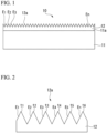
- Fig. 1 illustrates the mold of this embodiment.
- the mold 10 of this embodiment has a base material 11 of which the surface 11a is made of a planar sheet-like body, and a recessing and protruding layer 12 provided on the surface 11a of the base material 11.
- the size of the mold is selected as appropriate according to the optical element to be manufactured by the mold.
- the area of the surface 11a of the base material 11 is from 30 mm ⁇ 30 mm to 1100 mm ⁇ 1300 mm, and preferably from 200 mm ⁇ 200 mm to 400 mm ⁇ 500 mm.
- the base material 11 consists of stainless steel.
- the area of the surface 11a of the base material 11 is selected as appropriate according to the area of the optical element to be manufactured by the mold.
- the thickness of the base material 11 is not particularly limited provided that strength as a mold 10 can be maintained, but it may be, for example, from 0.1 mm to 100 mm, and preferably from 0.3 mm to 10 mm.
- the shape of the base material 11 is a flat body.
- the surface roughness (Ra) of the surface 11a is from 0.1 nm to 50 nm, and preferably from 0.1 nm to 10 nm.
- the recessing and protruding layer 12 is formed on the surface 11a.
- the recessing and protruding layer 12 is a layer of which the face that abuts the material of the optical element is a recessing and protruding face 12a.
- the recessing and protruding layer 12 be formed by a material containing at least one of (A) to (D) below.
- Cr, Mo, W, Ti, Ta, SiO 2 , TiO 2 , SiN, TiN, SiC, and WC are preferred due to the fact that film deposition is easier.
- the recessing and protruding layer 12 is preferably formed by a material containing (A1) and at least one of (B) to (D) below.
- Cr, Mo, W, Ti, Ta, SiO 2 , TiO 2 , SiN, TiN, SiC, and WC are preferred due to the fact that film deposition is easier. Furthermore, from the prospective of etching speed with respect to etching gas used in an etching step to be described later, Cr, W, SiN, TiN, and SiC are preferred.
- the combination of the material of the base material 11 and the material of the recessing and protruding layer 12 may be determined in consideration of adhesion during film deposition of the recessing and protruding layer 12 on the base material 11, strength, and the like.
- stainless steel is used as the base material 11 and the recessing and protruding layer 12 contains Ti, Cr, W, Ni.
- a modal pitch, modal height, and shape of the fine recesses and protrusions are determined according to the application of the optical element.
- the modal pitch of the fine recesses and protrusions is preferably adjusted according to the wavelength of light to be used. In this case, because visible light of wavelength from approximately 400 nm to 750 nm is used, the pitch of the recesses and protrusions is preferably from not less than 50 nm to not greater than 300 nm. Additionally, when the pitch of fine recesses and protrusions is from not less than 50 nm to not greater than 150 nm, diffracted light in the visible light region can be reduced.
- the recesses and protrusions having a modal pitch of not less than 500 nm and not greater than 5,000 nm is preferred.
- the modal pitch P of the protrusions E n on the recessing and protruding face is specifically determined as follows.
- an atomic force microscope (AFM) image is obtained for a square region whose edge length is from 30 to 40 times the modal pitch P.
- the modal pitch is approximately 300 nm
- an image of a region of 9 ⁇ m ⁇ 9 ⁇ m to 12 ⁇ m ⁇ 12 ⁇ m is obtained.
- waveform separation of the image is performed by Fourier transform, and a fast Fourier transform (FFT) image is obtained.
- FFT fast Fourier transform
- the distance from the zero-order peak to the first-order peak in the profile of the FFT image is determined. The reciprocal of the distance thus determined is the modal pitch P in that region.
- This process is performed in the same manner for not less than a total of 25 randomly chosen regions of the same area, and the modal pitch in each region is determined.
- the average of the modal pitches P 1 to P 25 of the not less than 25 regions obtained in this manner is the modal pitch P. Note that, at this time, regions that are at least 1 mm apart, and more preferably from 5 mm to 1 cm apart from each other are preferably chosen.
- the optimal aspect ratio of the fine recesses and protrusions is determined depending on the application of the optical element. For example, when producing a diffraction grating used in an organic EL or thin-film device using this mold, the aspect ratio of the protrusions E n in the recesses and protrusions is preferably from 0.1 to 1.0. For example, when producing an antireflective body using this mold, the aspect ratio of the protrusions E n in the recesses and protrusions is preferably from 0.5 to 4.0, and more preferably from 1.0 to 3.0.
- the aspect ratio is the value determined by modal height H / modal pitch P.
- the modal height H is specifically determined as follows.
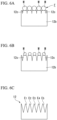
- a cross-section perpendicular to the substrate passing through the vertices of the protrusions E n along a line having a length of 1 mm in any direction at any position, i.e., the cross-section of Fig. 2 , is obtained from an AFM image.
- any portion of this cross-section containing not less than 30 protrusions E n is extracted, and for each of the protrusions E n contained therein, the difference between the height of its vertex and the height of the lowest position on a flat portion located between that protrusion E n and an adjacent E n is determined, the obtained value is rounded to the most significant two digits, and taking this as the height of each protrusion E n , the mode thereof is taken as the modal height H.
- the modal height H of the protrusions is preferably from 10 nm to 500 nm, and more preferably from 15 nm to 150 nm. When the modal height H is within the preferred range, an effect of improving the light extraction efficiency of the organic EL or thin-film device is obtained.
- the modal height H of the protrusions is preferably from 25 nm to 1200 nm, and more preferably from 120 nm to 500 nm.
- the modal height H of the protrusions is preferably from 250 nm to 10,000 nm, and more preferably from 750 nm to 10,000 nm. When the modal height H is within the preferred range, an effect of improving antireflective performance can be obtained.
- the recessing and protruding face 12a of the recessing and protruding layer 12 has a plurality of areas C 1 to C n , as illustrated in Fig. 3 .
- the areas C 1 to C n are regions continuously arranged in a positional relationship in which the central point of seven adjacent protrusions is an intersection point of diagonal lines of six vertices of a regular hexagon. Note that in Fig. 3 , for convenience, the position of the central point of each protrusion is indicated by a circle u centered on that central point.
- a positional relationship in which the central point of seven adjacent protrusions is an intersection point of diagonal lines of six vertices of a regular hexagon is, specifically, a relationship that satisfies the following conditions.
- a line segment L1 of a length equal to the modal pitch P is drawn from one central point t1 (refer to Fig. 2 ) toward an adjacent central point t2. Then, line segments L2 to L6 of lengths equal to the modal pitch P are drawn from the central point t1 in directions 60°, 120°, 180°, 240°, and 300° with respect to the line segment L1.
- the central point of these seven protrusions is in a positional relationship so that the central point is an intersection point of diagonal lines of six vertices of a regular hexagon.
- the modal area Q of the areas C 1 to C n (the mode of the area size) is preferably in the following range.
- the modal area Q within a 10 mm ⁇ 10 mm AFM image measurement range is preferably from 0.026 ⁇ m 2 to 6.5 2 mm .
- the modal area Q within a 10 mm ⁇ 10 mm AFM image measurement range is preferably from 0.65 pm 2 to 26 mm 2 .
- the modal area Q within a 50 mm ⁇ 50 mm AFM image measurement range is preferably from 2.6 ⁇ m 2 to 650 mm 2 .
- the modal area Q is within the preferred range, it is easier to suppress the color shift of the light.
- the areas C 1 to C n have random areas, shapes, and crystal orientations (orientation of a hexagonal lattice created by the particle arrangement), as illustrated in Fig. 3 .
- the lattice orientation of the areas C 1 to C n signifies the direction of a primitive translation vector (of which two exist in the case of a triangular lattice) obtained by connecting the vertices of adjacent protrusions in the same area when viewed from the top face of the substrate. Due to the fact that the area, shape, and crystal orientation of each of the areas C 1 to C n are random, diffracted light can be equalized and directionality can be reduced, and, when the article obtained from this mold is an antireflective body, color shifting can be suppressed. Also, when the article obtained from this mold is a grating structure used in an organic EL device or the like, anisotropy of the grating effect can be reduced.
- the degree of randomness of area preferably satisfies the following conditions.
- the standard deviation of ⁇ ab within a 10 mm ⁇ 10 mm AFM image measurement range is preferably not less than 0.08 ⁇ m 2 .
- the standard deviation of ⁇ ab within a 10 mm ⁇ 10 mm AFM image measurement range is preferably not less than 1.95 ⁇ m 2 .
- the standard deviation of ⁇ ab within a 50 mm ⁇ 50 mm AFM image measurement range is preferably not less than 8.58 ⁇ m 2 .
- the standard deviation of the ratio of a to b (a / b) in the above formula ( ⁇ ) is preferably not less than 0.1.
- the randomness of the crystal orientation of the areas C 1 to C n preferably satisfies the following conditions.
- a straight line K0 is drawn connecting the central points of any two adjacent protrusions in any area (I). Then, one area (II) adjacent to the area (I) is chosen, and six straight lines K1 to K6 are drawn connecting any protrusion in area (II) and the central points of six protrusions adjacent to that protrusion. When all of lines K1 to K6 are at an angle of not less than 3 degrees with respect to the straight line K0, it is defined that the crystal orientations of area (I) and area (II) are different.
- areas adjacent to area (I) there are preferably not less than two areas having a different crystal orientation than area (I), and more preferably not less than three such areas, and even more preferably not less than five such areas.
- the recesses and protrusions of the recessing and protruding layer 12 that constitutes the above mold for manufacturing an optical element 10 are random to an appropriate degree. Accordingly, directionality of diffracted light can be reduced and color shifting can be suppressed despite recesses and protrusions having a fine pitch being provided such that diffracted light is produced.
- the recesses and protrusions of the recessing and protruding layer 12 are not completely random, and have a certain order within the range of each of the areas C 1 to C n . Accordingly, the pitch of the recesses and protrusions can be easily adjusted, and the targeted optical function can be easily obtained.
- the production method of this embodiment has a film deposition step, a particle arrangement step, and an etching step.
- the film deposition step is a step in which an inorganic film which will subsequently become the recessing and protruding layer 12 is deposited on the surface 11a of the base material 11.
- the film deposition method of the inorganic film in the film deposition step may be any of physical vapor deposition (PVD) such as sputtering or vacuum deposition, chemical vapor deposition (CVD), or plating (electrolytic, electroless), but sputtering is preferred from the perspective of film deposition characteristics.
- PVD physical vapor deposition
- CVD chemical vapor deposition
- plating electrolytic, electroless
- an inorganic film formed by sputtering has the feature of strong adhesive strength with respect to the base material compared to those formed by CVD or plating.
- An inorganic film formed by CVD has the feature of good film crystallinity compared to those formed by sputtering or plating.
- An inorganic film formed by plating has the feature of being able to form dense layers compared to those formed by sputtering or CVD.
- a method for depositing an inorganic film by sputtering that can be applied is a method wherein an inert gas such as argon gas is made to collide with a target of the same components as the recessing and protruding layer 12 formed by the production method, thereby accumulating atoms flying from the target on the surface 11a.
- an inert gas such as argon gas
- sputtering is performed so that inert gas is made to collide with a target containing at least one element selected from the group consisting of Si, Cr, Mo, W, Ta, Ni, and Ti in an atmosphere containing at least one of oxygen and nitrogen, thereby allowing that element, which flies from the target, and at least one of the oxygen and nitrogen in the atmosphere to be accumulated on the surface 11a.
- sputtering is performed so that inert gas is made to collide with a target containing at least one element selected from the group consisting of Si, Cr, Mo, W, Ta, and Ti in an atmosphere containing at least one of oxygen and nitrogen, thereby allowing that element, which flies from the target, and at least one of the oxygen and nitrogen in the atmosphere to be accumulated on the surface 11a.
- the oxygen atom content in the inorganic film can be adjusted according to the concentration of oxygen in the atmosphere.
- the nitrogen atom content in the inorganic film can be adjusted according to the concentration of nitrogen in the atmosphere.
- a known method of sputtering may be used without particular limitation, but magnetron sputtering is preferred due to its excellent film deposition characteristics.
- the sputtering conditions are not particularly limited, but normally, the temperature is from 25.0°C to 250°C, and the absolute pressure is from 0.1 Pa to 3.0 Pa.
- the sputtering time is adjusted such that the thickness of the inorganic film is from 0.1 ⁇ m to 10.0 ⁇ m.
- the particle arrangement step is a step in which a plurality of particles is arranged in a monolayer on a surface of the inorganic film obtained in the film deposition step.
- the particle arrangement step in this embodiment is performed by a method that employs the concept of the Langmuir-Blodgett (LB) method.
- the particle arrangement step in this embodiment wherein a single-particle film is disposed on an inorganic film as a mask, has a dripping step, a single-particle film formation step, a transfer step, and, as necessary, an affixation step.
- the dripping step is a step in which a dispersion having particles dispersed in a solvent of lower specific gravity than water is dripped on the surface of water in a water tank.
- the single-particle film formation step is a step in which a single-particle film made of the above particles is formed on the surface of water by volatilizing the solvent.
- the transfer step is a step in which the above single-particle film is transferred to the inorganic film.
- the affixation step is a step in which the transferred single-particle film is affixed to the inorganic film.
- a dispersion is prepared by adding particles M to a solvent of lower specific gravity than water. Meanwhile, a water tank (trough) is prepared, and water for expanding the particles M on the surface thereof (hereinafter sometimes referred to as "lower-layer water”) is put in the tank.
- the surface of the particles M is preferably hydrophobic. It is also preferable to select a hydrophobic solvent. By combining the hydrophobic particles M and solvent with the lower-layer water, self-assembly of the particles M progresses, as will be described later, and a two-dimensionally close-packed single-particle film is formed.
- the material of the particles M is at least one type of particle selected from the group consisting of organic particles, organic-inorganic composite particles, and inorganic particles.
- the material that forms the organic particles is at least one type selected from the group consisting of thermoplastic resins such as polystyrene or PMMA, thermosetting resins such as phenol resins or epoxy resins, diamond, graphite, and fullerenes.
- the material that forms the organic-inorganic composite particles is at least one type selected from the group consisting of, for example, SiC and boron carbide.
- the material of the particles M is preferably inorganic particles.
- the material that forms the inorganic particles is at least one type selected from the group consisting of, for example, inorganic oxides, inorganic nitrides, inorganic borides, inorganic sulfides, inorganic selenides, metal compounds, and metals.
- the inorganic oxide is at least one type selected from the group consisting of, for example, silica, alumina, zirconia, titania, ceria, zinc oxide, tin oxide, and yttrium aluminum garnet (YAG).
- the inorganic nitride is at least one type selected from the group consisting of, for example, silicon nitride, aluminum nitride, and boron nitride.
- the inorganic boride is at least one type selected from the group consisting of, for example, ZrB 2 and CrB 2 .
- the inorganic sulfide is at least one type selected from the group consisting of, for example, zinc sulfide, calcium sulfide, cadmium sulfide, and strontium sulfide.
- the inorganic selenide is at least one type selected from the group consisting of, for example, zinc selenide and cadmium selenide.
- the metal particles are at least one type of particle selected from the group consisting of Si, Ni, W, Ta, Cr, Ti, Mg, Ca, Al, Au, Ag, and Zn.
- the material that forms the particles M may be a sialon, constituted of silicon, aluminum, oxygen, and nitrogen.
- the particles M may be a mixture of particles of not less than two different materials.
- the particles M may be a laminate made of different materials, e.g., particles obtained by coating inorganic particles made of an inorganic nitride with an inorganic oxide.
- the particles M may be fluorescent particles in which an activator such as cerium or europium has been introduced into an inorganic particle.
- the material that forms the particles M is preferably an inorganic oxide due to the fact that the shape of the particles M is stable, and among inorganic oxides, silica, titania, alumina, and zirconia are more preferred.
- Hydrophobic solvents that have high volatility include volatile organic solvents made of not less than one type selected from chloroform, methanol, ethanol, isopropanol, acetone, methyl ethyl ketone, ethyl ethyl ketone, methyl isobutyl ketone, toluene, hexane, cyclohexane, ethyl acetate, butyl acetate, and the like.
- the particles M are inorganic particles, it is normally preferred that they be used after being hydrophobized using a hydrophobizing agent because the surface thereof is hydrophilic.
- a hydrophobizing agent surfactants, metal alkoxysilane, and the like may be used.
- Hydrophobizing of the particles M may be performed using a surfactant, metal alkoxysilane, or the like similar to the hydrophobizing agent described in Japanese Unexamined Patent Application Publication No. 2009-162831A , by a similar method.
- a microfilter such as a membrane filter to remove aggregated particles (secondary particles made of a plurality of primary particles) present in the dispersion before it is dripped onto the liquid surface.
- aggregated particles secondary particles made of a plurality of primary particles
- the dispersion described above is dripped onto the surface of the lower-layer water (dripping step).
- the solvent that is the dispersion medium volatilizes and the particles M expand in a monolayer on the surface of the lower-layer water, and a two-dimensionally close-packed single-particle film can be formed (single-particle film formation step).
- the particle concentration of the dispersion dripped onto the lower-layer water is preferably from 1% by mass to 10% by mass with respect to the total dispersion.
- the dripping rate is preferably from 0.001 mL/s to 0.01 mL/s.
- the single-particle film is formed by self-assembly of the particles M.
- the principle behind this is that when particles accumulate, surface tension caused by the dispersion medium present between particles acts, and as a result, the particles M automatically form a two-dimensionally close-packed structure rather than existing randomly. As another expression, this close packing due to such surface tension is also called ordering by lateral capillary forces.
- the single-particle film formation step is preferably performed under ultrasonic irradiation conditions.
- the solvent of the dispersion is volatilized while irradiating the water surface with ultrasonic waves from the lower-layer water, close packing of the particles M is promoted, and a single-particle film in which the particles M are two-dimensionally close-packed with higher precision is obtained.
- the power of the ultrasonic waves is preferably from 1 W to 1,200 W, and more preferably from 50 W to 600 W.
- the frequency of the ultrasonic waves is not particularly limited, but is preferably, for example, from 28 kHz to 5 MHz, and more preferably from 700 kHz to 2 MHz.
- the frequency is too high, it is undesirable because the water molecules start to absorb energy and the phenomenon of water vapor or droplets rising from the water surface occurs.
- the frequency is too low, the cavitation radius in the lower-layer water becomes large, and bubbles are produced in the water and float up toward the surface. When such bubbles accumulate below the single-particle film, it is problematic because the water surface is no longer flat.
- a standing wave is generated at the water surface by ultrasonic irradiation. Attention is required because, no matter what the frequency, when the power is too high and the wave height on the water surface becomes too high depending on the tuning conditions of the ultrasonic transducer and the transmitter, the single-particle film will be broken by the surface wave.
- the characteristic frequency calculated from the size of the particles can be used as a benchmark.
- the characteristic frequency ends up being extremely high, and it is therefore difficult to provide the calculated ultrasonic vibration.
- the calculation is performed assuming characteristic vibration corresponding to a mass ranging from a dimer to a 20-mer, the required frequency can be reduced to a practical range.
- a particle packing efficiency improving effect also occurs even when ultrasonic vibration corresponding to the characteristic frequency of an assembly of particles is provided.
- the ultrasonic irradiation time may be any duration provided that it is sufficient for particle rearrangement to be completed, and the required time varies depending on particle size, ultrasonic frequency, water temperature, and the like. However, under normal production conditions, from 10 seconds to 60 min is preferred, and from 3 min to 30 min is more preferred.
- the advantages gained by ultrasonic irradiation are close packing of particles (hexagonal close packing of random arrangement), as well as an effect of destroying soft aggregates of particles readily generated during preparation of the nanoparticle dispersion, and an effect of repairing point defects, line defects, or crystal dislocations (local distortions of unit lattice occurring due to disturbance of particle arrangement) to a certain degree once they have occurred.
- A is the average particle size of the particles M
- B is the modal pitch between the particles M.
- indicates the absolute value of the difference between A and B.
- Divergence D is more preferably not greater than 10%, and even more preferably from 1.0% to 3.0%.
- the average particle size A of the particles M is the average primary particle size of the particles M that constitute the single-particle film, which can be determined by a commonly used method from the peak obtained by fitting the particle size distribution determined by particle dynamic light scattering to a Gaussian curve.
- the pitch between the particles M is the distance from vertex to vertex of two adjacent particles M
- the modal pitch B is the modal value thereof. Note that when the particles M are spherical and abut without a gap, the distance from vertex to vertex of adjacent particles M is equal to the distance from center to center of adjacent particles M.
- the modal pitch B between the particles M is determined as follows.
- an atomic force microscope image is obtained for a square region whose edge length is from 30 to 40 times the modal pitch B between the particles M.
- an image of a region from 9 ⁇ m ⁇ 9 ⁇ m to 12 ⁇ m ⁇ 12 ⁇ m is obtained.
- waveform separation of the image is performed by Fourier transform, and a fast Fourier transform (FFT) image is obtained.
- FFT fast Fourier transform
- This process is performed in the same manner for not less than a total of 25 randomly chosen regions of the same area, and the modal pitches B 1 to B 25 of the regions are determined.
- the average of the modal pitches B 1 to B 25 of the not less than 25 regions obtained in this manner is the modal pitch B.
- regions that are at least 1 mm apart, and more preferably from 5 mm to 1 cm apart from each other are preferably chosen.
- the divergence D of this arrangement is an indicator of the degree of close packing of the particles M. That is, a low divergence D of particle arrangement means that the degree of close packing is high, the gaps between particles are controlled, and the precision of their arrangement is high.
- the coefficient of variation of particle size of the particles M is preferably from 0.1% to 20%, more preferably from 0.1% to 10%, and even more preferably from 0.1% to 5.0%.
- the modal pitch between the particles M is equal to the modal pitch of the recesses and protrusions of the recessing and protruding layer. Because the arrangement of the particles M has a high degree of close packing, the average particle size A of the particles M are appropriately selected, so that the modal pitch between particles can be adjusted and the modal pitch of the recesses and protrusions can be adjusted.
- the single-particle film that has been formed on a liquid surface in the single-particle film formation step is then transferred to the inorganic film in the single-layer state as-is (transfer step).
- the specific method for transferring the single-particle film to the inorganic film is not particularly limited, and examples thereof include a method wherein the surface of the inorganic film provided on the base material is lowered from above and put in contact with the single-particle film while being held substantially perpendicular to the single-particle film, and the single-article film is transferred to the inorganic film by the affinity force between the hydrophobic single-particle film and the inorganic film; and a method wherein the inorganic film provided on the base material is disposed in a substantially perpendicular direction in the lower-layer water in a water tank prior to forming the single-particle film, and after the single-particle film is formed on the liquid surface, the single-particle film is transferred to the inorganic film by gradually lowering the liquid level.
- the single-particle film can be transferred to the inorganic film without using special equipment by either of the above methods, but the so-called LB trough method is preferably employed in the subsequent step because even if the single-particle film has a larger area, it is easily transferred to the inorganic film while maintaining its two-dimensionally close-packed state (refer to Journal of Materials and Chemistry, Vol. 11, 3333 (2001 ), Journal of Materials and Chemistry, Vol. 12, 3268 (2002 ), and the like).
- Figs. 5A and 5B schematically illustrate an outline of the LB trough method. Note that, in Figs. 5A and 5B , the particles M are greatly enlarged for the sake of convenience.
- a workpiece S in which an inorganic film 12b is provided on the base material 11, is immersed in advance in lower-layer water W in water tank V such that the surface of the inorganic film 12b is substantially vertical, and in that state, the above dripping step and single-particle film formation step are performed, and a single-particle film F is formed ( Fig. 5A ). Then, after the single-particle film formation step, the workpiece S is raised upward while the surface of the inorganic film 12b remains vertical, so that the single-particle film F can be transferred to the surface of the inorganic film 12b ( Fig. 5B ).
- the figures illustrate the state where the single-particle film F is transferred to both side faces of the workpiece S, but the recessing and protruding structure may be formed only on one side face X of the workpiece S. It is preferred that the single-particle film F be transferred only to the side face X in a state where wrap-around of the particles M from the side face X to the rear face is prevented by shielding the face (rear face) on the side opposite the one side face X of the workpiece S with a thick plate so that the single-particle film F can be transferred more precisely. However, it is permissible if it is transferred to both faces.
- the single-particle film F has already been formed into a monolayer on the liquid surface in the single-particle film formation step, there is no risk of the single-particle film F being destroyed so as to be multilayered in the transfer step even if the temperature conditions of the transfer step (temperature of lower-layer water) or the raising speed of the workpiece fluctuate somewhat.
- the temperature of the lower-layer water is normally approximately from 10°C to 30°C, depending on the ambient temperature which normally fluctuates depending on season and weather.
- an LB trough device equipped with a surface pressure sensor (not illustrated) that uses the principle of a Wilhelmy plate or the like, which measures the surface pressure of the single-particle film F, and a moveable barrier (not illustrated), which compresses the single-particle film F in the direction along the liquid surface, is used as the water tank V, so that a single-particle film F of a larger area can be transferred to the inorganic film 12b more stably.
- the single-particle film F can be compressed to a preferred diffusion pressure (density) while the surface pressure of the single-particle film F is measured, and additionally, it can be moved at a constant speed toward the inorganic film 12b.
- the diffusion pressure is preferably from 5 mNm -1 to 80 mNm -1 , and more preferably from 10 mNm -1 to 40 mNm -1 .
- the speed at which the workpiece S is raised is preferably from 0.5 mm/min to 20 mm/min.
- the temperature of the lower-layer water is normally from 10°C to 30°C.
- the LB trough device used can be a commercially available product.
- the single-particle film F be transferred to the inorganic film 12b in the state in which the single-particle film F has the particles two-dimensionally close-packed with as high precision as possible in this manner, but no matter how carefully the operation is performed, 100% complete close packing is not achieved, and the particles transferred to the inorganic film 12b end up in a polycrystalline state.
- a polycrystalline state means a state in which the lattice orientation of the particles M is uniform within each of the areas C 11 to C 1n , but it is not macroscopically uniform.
- a recessing and protruding structure having a plurality of areas continuously arranged in a positional relationship in which the central point of seven adjacent protrusions is an intersection point of diagonal lines of six vertices of a regular hexagon.
- the single-particle film F of the particles M can be transferred to the inorganic film 12b by the transfer step, but after the transfer step, an affixation step may be performed to affix the transferred single-particle film F to the inorganic film 12b.
- an affixation step may be performed to affix the transferred single-particle film F to the inorganic film 12b.
- the possibility of the particles M moving on the inorganic film 12b is reduced, and etching can be performed more stably and with higher precision.
- Methods for the affixation step include a method in which binder is used and a sintering method.
- a binder solution is supplied to the inorganic film 12b on which the single-particle film has been formed, and is made to penetrate between the inorganic film 12b and the particles M that constitute the single-particle film.
- the amount of binder to be used is preferably from 0.001 to 0.02 times the mass of the single-particle film. If within such a range, the particles can be adequately affixed without the problem of excessive binder clogging the gaps between the particles M and adversely affecting the precision of the single-particle film.
- the excess binder solution can be removed by using a spin coater or by tilting the workpiece.
- the binder may include a metal alkoxysilane mentioned previously as a hydrophobizing agent, general organic binder, inorganic binder, and the like. After the binder solution penetrates, appropriate heat treatment may be performed in accordance with the type of binder. When a metal alkoxysilane is used as a binder, heat treatment is preferably performed for from 3 min to 60 min at from 40°C to 80°C.
- the inorganic film on which the single-particle film has been formed may be heated to fuse the particles M that constitute the single-particle film to the inorganic film.
- the heating temperature can be determined according to the material of the particles M and the material of the inorganic film, but with the particles M of particle size not greater than 1,000 nm, sintering is completed at a relatively low temperature because an interfacial reaction begins at a temperature lower than the original melting point of those substances.
- the heating temperature is too high, the fusion area of the particles becomes large, resulting in the possibility of affecting precision, such as the shape of the single-particle film changing.
- the etching step is a step in which the inorganic film is dry-etched using the plurality of particles M as an etching mask.
- etching gas passes through the gaps between the particles M that constitute the single-particle film F and reaches the surface of the inorganic film 12b, so that grooves are formed in that portion, and round pillars 12c appear at the respective positions corresponding to the particles M. Then, as etching continues, the particles M on the round pillars 12c are gradually etched and become small, and at the same time, the grooves in the inorganic film 12b become deeper ( Fig. 6B ). Then, finally, the particles M disappear due to etching, and a plurality of conical protrusions E n are formed on one face of the inorganic film 12b ( Fig. 6C ).
- etching gas used in dry etching examples include Ar, SF 6 , F 2 , CF 4 , C 4 F 8 , C 5 F 8 , C 2 F 6 , C 3 F 6 , C 4 F 6 , CHF 3 , CH 2 F 2 , CH 3 F, C 3 F 8 , Cl 2 , CCl 4 , SiCl 4 , BCl 2 , BCl 3 , BC 2 , Br 2 , Br 3 , HBr, CBrF 3 , HCl, CH 4 , NH 3 , O 2 , H 2 , N 2 , CO, CO 2 , and the like, and one or more of these may be used in accordance with the material of the particles that constitute the single-particle film mask and the material of the inorganic film.
- a device capable of anisotropic etching such as a reactive ion etching device, ion beam etching device, or the like, is used. Provided that it can generate a bias electric field of at least approximately 20 W, the etching device is not particularly limited in its specifications such as plasma generation mode, electrode structure, chamber structure, the frequency of a high-frequency power source, and the like.
- Etching conditions may be selected as appropriate according to the aspect ratio of the recesses and protrusions to be obtained.
- Examples of etching conditions include bias power, antenna power, gas flow rate and pressure, etching time, and the like.
- A is the average particle size of the particles that constitute the used single-particle film etching mask.
- a mold in which recesses and protrusions having a plurality of areas of random area, shape, and crystal orientation are formed can be produced.
- mold production can be simplified because the above production method is a method in which recesses and protrusions are directly formed on an inorganic film provided on the surface of a base material rather than a method in which recesses and protrusions are transferred by electroforming. Additionally, fine recesses and protrusions can be formed on the surface of a mold for injection molding as well, and it is also possible to produce a sheet-like optical element on which recesses and protrusions have been formed on both faces.
- nanoimprinting As the method for producing an optical element using the above mold, nanoimprinting, press molding, injection molding, electroforming, and the like may be used.
- a shape transfer body in which a periodic grating structure is formed with high precision that is advantageous in achieving a viewing angle restriction function can be produced in high quantity with good reproducibility.
- nanoimprinting and injection molding are preferred due to being particularly suited to transfer of fine recesses and protrusions.
- an optical imprinting device equipped with, for example, pressing means for pressing the mold against the photocurable resin and irradiation means for irradiating the photocurable resin with active energy rays may be used.
- the recessing and protruding face 12a of the sheet-like mold 10 is coated with uncured liquid active energy ray-curable resin to a thickness of from 0.5 ⁇ m to 20 ⁇ m, and preferably from 1.0 ⁇ m to 10 ⁇ m.
- the mold 10 coated with the curable resin passes through a pair of rollers so as to be pressed, and the curable resin is packed into the recesses and protrusions of the mold 10.
- the active energy ray irradiation device radiates active energy rays at from 10 mJ to 5,000 mJ, and preferably from 100 mJ to 2,000 mJ, thereby crosslinking and/or curing the curable resin.
- the cured active energy ray-curable resin is peeled from the mold 10 to produce an optical element.
- a layer made of silicone resin, fluorine resin, or the like may be provided on the recessing and protruding face 12a of the mold 10 to a thickness of from 1 nm to 10 nm before the recessing and protruding face 12a is coated with the uncured active energy ray-curable resin.
- the uncured active energy ray-curable resin examples include those containing one or more components selected from prepolymers such as an epoxy acrylate, an epoxidized oil acrylate, an urethane acrylate, an unsaturated polyester, a polyester acrylate, a polyether acrylate, a vinyl/acrylate, a polyene/acrylate, a silicon acrylate, a polybutadiene, and a polystyrene methyl methacrylate; and monomers such as an aliphatic acrylate, an alicyclic acrylate, an aromatic acrylate, a hydroxyl group-containing acrylate, an allyl group-containing acrylate, a glycidyl group-containing acrylate, a carboxy group-containing acrylate, and a halogen-containing acrylate.
- the uncured active energy ray-curable resin is preferably used after appropriate dilution with a solvent such as ethyl acetate, methyl e
- a fluorine resin, a silicone resin, and the like may also be added to the uncured active energy ray-curable resin.
- the uncured active energy ray-curable resin is cured by ultraviolet rays
- a photopolymerization initiator such as acetophenones or benzophenones
- At least one of a polyfunctional (meth) acrylate monomer and oligomer may also be added to the uncured active energy ray-curable resin with the objective of increasing hardness after curing. Furthermore, it may also contain reactive inorganic oxide particles and/or reactive organic particles.
- the uncured active energy ray-curable resin after being applied is bonded with an adhesive base made of resin, glass, or the like and then is irradiated with active energy rays.
- Active energy rays may be radiated from either the adhesive base or the mold 10 having active energy ray permeability.
- the sheet thickness of the cured active energy ray-curable resin is preferably from 0.1 ⁇ m to 100 ⁇ m.
- the sheet thickness of the cured active energy ray-curable resin is not less than 0.1 ⁇ m, adequate strength can be assured, and when not greater than 100 ⁇ m, adequate flexibility can be assured.
- examples of the liquid thermosetting resin include uncured melamine resin, urethane resin, epoxy resin, and the like.
- the heating conditions can be determined as appropriate according to the characteristics of the liquid thermosetting resin.
- examples of the liquid inorganic material include uncured silicon oxide-based sol-gel material, polydimethylsiloxane, polysilsesquioxane, and the like.
- the heating conditions can be determined as appropriate according to the characteristics of the liquid inorganic material.
- the heating temperature be from 100°C to 500°C and the heating time be from 20 min to 60 min. Furthermore, when polysilsesquioxane is used, it is preferable that the heating temperature be from 100°C to 200°C and the heating time be from 10 min to 60 min.
- thermo imprinting device equipped with, for example, pressing means for pressing the mold against the thermoplastic resin and temperature control means for controlling the temperature of the thermoplastic resin may be used.
- thermoplastic resin examples include an acrylic resin, a polyolefin, a polyester, and the like.
- the pressure when pressing the sheet-like thermoplastic resin into a molded article for a secondary step is preferably from 1 MPa to 100 MPa.
- the pressure during pressing is not less than 1 MPa, the recesses and protrusions can be transferred with high precision, and when not greater than 100 MPa, excessive pressure can be prevented.
- the heating conditions can be determined as appropriate according to the characteristics of the thermoplastic resin. It is preferable that the heating temperature be from 120°C to 200°C and the pressing time be from 1 min to 5 min.
- the cooling temperature after heating is preferably below the glass transition temperature of the thermoplastic resin, because the recesses and protrusions are transferred with high precision.
- method (a) which uses active energy ray-curable resin is preferred because heating can be omitted and it is simple.
- the mold of the above embodiment is used as part of the mold for injection molding that forms a cavity. That is, the above mold is arranged on the inner face of the cavity.
- thermoplastic resin is melted using an injection molder on which a mold for injection molding is mounted. Then, the melted thermoplastic resin is injected at high pressure into the cavity of the mold for injection molding, and then the mold for injection molding is cooled. The mold for injection molding is then opened, and the obtained optical element is removed.
- thermoplastic resin molded by injection molding the same thermoplastic resins as used in the above thermal imprinting method may be used.
- optical elements that can be produced using the above mold include diffraction gratings used in organic EL and thin-film devices, antireflective bodies, and the like.
- the optical element formed by the above method is a diffraction grating, it has a light-emitting face having recesses and protrusions corresponding to the mold 10 at least on the face from which light is emitted to the outside.
- the optical element when it is a diffraction grating, it may be used as a substrate of organic EL lighting and the like.
- the optical element when it is an antireflective body, it may be used as a lens used in optical equipment or the full panel of an image display device.
- the modal pitch, modal height, and shape of the fine recesses and protrusions of the light-emitting face of the optical element formed by the above method are determined depending on the application of the optical element.
- the modal pitch of the fine recesses and protrusions is preferably adjusted according to the wavelength of light incident on the antireflective body. For example, when visible light of wavelength from approximately 400 nm to 750 nm is used, the pitch of the recesses and protrusions is preferably from not less than 50 nm to not greater than 300 nm.
- the pitch of fine recesses and protrusions is from not less than 50 nm to not greater than 150 nm, diffracted light in the visible light region can be reduced.
- the modal pitch of the recesses and protrusions is preferably from not less than 500 nm to not greater than 5,000 nm.
- the optimal aspect ratio of the fine recesses and protrusions is determined depending on the application of the optical element.
- the aspect ratio of the protrusions E n in the recesses and protrusions is preferably from 0.1 to 1.0.
- the aspect ratio of the protrusions E n in the recesses and protrusions is preferably from 0.5 to 4.0, and even more preferably from 1.0 to 3.0.
- the modal height H of the protrusions is preferably from 10 nm to 500 nm, and more preferably from 15 nm to 150 nm. When the modal height H is within the preferred range, an effect of improving the light extraction efficiency of the organic EL or thin-film device is obtained.
- the modal height H of the protrusions is preferably from 25 nm to 1,200 nm, and more preferably from 120 nm to 500 nm.
- the modal height H of the protrusions is preferably from 250 nm to 10,000 nm, and more preferably from 750 nm to 10,000 nm. When the modal height H is within the preferred range, an effect of improving antireflective performance can be obtained.
- the recesses and protrusions of the above optical element are random to an appropriate degree. Accordingly, directionality of diffracted light can be reduced and color shifting can be suppressed despite recesses and protrusions having a fine pitch being provided such that diffracted light is produced.
- the recesses and protrusions of the optical element are not completely random, and have a certain order within the range corresponding to each of the areas C l to C n . Accordingly, the pitch of the recesses and protrusions of the optical element can be easily adjusted, and the targeted optical function can be easily obtained.
- the shape of the base material 11 is a planar sheet-like body.
- a mold 20A in this embodiment includes a base material 21A having a convex curved face.
- a mold 20B in this embodiment includes a base material 21B having a concave curved face.
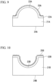
- the mold 20A of this embodiment has, as illustrated in Fig. 9 , the base material 21A of which a surface 23A has a convex curved face, and a recessing and protruding layer 22A provided on the surface 23A of the base material 21A.
- the mold 20B of this embodiment has, as illustrated in Fig. 10 , the base material 21B of which a surface 23B has a concave curved face, and a recessing and protruding layer 22B provided on the surface 23A of the base material 21B.
- the materials of the base materials 21A and 21B consist of stainless steel.
- the surface 23A has a convex curved face.
- the convex curved face may be a parabolic face or a spherical face.
- the shape of the convex curved face when viewed from the direction perpendicular to a surface 24A does not necessarily have to be round, and may be a shape of a circle being elongated along one axis or a plurality of axes.
- the length of the long axis of the convex curved face may be from 30 mm to 1300 mm, and is preferably from 200 mm to 500 mm.
- the radius of curvature in the cross-section along the long axis may be from 30 mm to 3,000 mm, and is preferably from 50 mm to 1,000 mm.
- the shape of the surface 23A is obtained by machining the surface of the base material 21A using a method such as pressing, cutting, or grinding.
- the surface 24A located opposite the surface 23A may be a flat face.
- the surface 23B has a concave curved face.
- the concave curved face may be a parabolic face or a spherical face.
- the shape of the concave curved face when viewed from the direction perpendicular to the surface 24B does not necessarily have to be round, and may be a shape of a circle being elongated along one axis or a plurality of axes.
- the length of the long axis of the concave curved face may be from 30 mm to 1300 mm, and is preferably from 200 mm to 500 mm.
- the radius of curvature in the cross-section along the long axis may be from 30 mm to 3,000 mm, and is preferably from 50 mm to 1,000 mm.
- the surface 24B located opposite the surface 23B may be a flat face.
- the shape of the surface 23B is obtained by machining the surface of the base material 21B using a method such as pressing, cutting, or grinding.
- the recessing and protruding layer 22A is a layer of which the face that abuts the material of the optical element is a recessing and protruding face 25A.
- the recessing and protruding layer 22B is a layer of which the face that abuts the material of the optical element is a recessing and protruding face 25B.
- the recessing and protruding layers 22A and 22B are the same as the recessing and protruding layer 12 described in the first embodiment except that they are formed on the surface 23A or 23B having a convex curved face or concave curved face.
- the axial direction of the recesses and protrusions of the recessing and protruding face 25A or 25B formed on the surface is close to the direction perpendicular to the surface 24A or 24B (the recessing and protruding layer 22A or 22B is the face that abuts the surface 24A or 24B).
- the molds 20A and 20B for manufacturing an optical element of this embodiment are formed using the method for creating the recessing and protruding layers 22A and 22B to be described later, the pitch of the recesses and protrusions can be easily adjusted and the targeted optical function can be easily obtained even when there are recesses and protrusions on the surface as in the base materials 21A and 21B. Accordingly, directionality of diffracted light can be reduced and color shifting can be suppressed despite recesses and protrusions having a fine pitch being provided such that diffracted light is produced.
- the production method of this embodiment similar to the first embodiment, has a film deposition step, a particle arrangement step, and an etching step. A description of a step which is the same as in the first embodiment will be omitted. Note that in the description below, a method for producing the mold 20A is described as an example.
- the film deposition step is a step in which an inorganic film which will subsequently become the recessing and protruding layer 22A is deposited on the surface 23A of the base material 21A.
- the film deposition method of the inorganic film in the film deposition step may be any of physical vapor deposition (PVD) such as sputtering or vacuum deposition, chemical vapor deposition (CVD), or plating (electrolytic, electroless), but sputtering is preferred from the perspective of film deposition characteristics on the surface 23A, which has a convex face.
- PVD physical vapor deposition
- CVD chemical vapor deposition
- plating electrolytic, electroless
- the particle arrangement step and the affixation step are the same as in the first embodiment.
- the etching step is a step in which the inorganic film is dry-etched using the plurality of particles M as an etching mask.
- the specific method of the etching step is the same as in the first embodiment.
- etching gas passes through the gaps between the particles M that constitute the single-particle film F and reaches the surface of the inorganic film 12b, so that grooves are formed in that portion, and round pillars 12c appear at the respective positions corresponding to the particles M. Then, as etching continues, the particles M on the round pillars 12c are gradually etched and become small, and at the same time, the grooves in the inorganic film 12b become deeper ( Fig. 11B ). Then, finally, the particles M disappear due to etching, and a plurality of conical protrusions E n are formed on one face of the inorganic film 12b ( Fig. 11C ).
- the etching gas used in dry etching is the same as in the first embodiment.
- the etching device that performs dry etching and the etching conditions are also the same as in the first embodiment.
- a mold in which recesses and protrusions having a plurality of areas of random area, shape, and crystal orientation are formed can be produced.
- mold production can be simplified because the above production method is a method in which recesses and protrusions are directly formed on an inorganic film provided on the surface of a base material rather than a method in which recesses and protrusions are transferred by electroforming. Additionally, according to the above production method, fine recesses and protrusions can be formed on the surface of a mold for injection molding as well, and it is also possible to produce a sheet-like optical element on which recesses and protrusions have been formed on both faces.
- the thickness of the etching mask can be made substantially constant even when there are recesses and protrusions on the surface as in the base materials 21A and 21B.
- the pitch of the recesses and protrusions on the recessing and protruding layer can be adjusted to a targeted value.
- nanoimprinting As the method for manufacturing an optical element using the above mold, nanoimprinting, press molding, injection molding, electroforming, and the like may be used.
- a shape transfer body in which a periodic grating structure is formed with high precision that is advantageous in achieving a viewing angle restriction function can be produced in high quantity with good reproducibility.
- nanoimprinting and injection molding are preferred due to being particularly suited to transfer of fine recesses and protrusions.
- the modal pitch, modal height, and shape of the fine recesses and protrusions of the light-emitting face of the optical element formed by the above method are determined depending on the application of the optical element.
- the modal pitch of the fine recesses and protrusions is preferably adjusted according to the wavelength of light to be used. For example, when visible light of wavelength from approximately 400 nm to 750 nm is used, the pitch of the recesses and protrusions is preferably from not less than 50 nm to not greater than 300 nm.
- the pitch of fine recesses and protrusions is from not less than 50 nm to not greater than 150 nm, diffracted light in the visible light region can be reduced.
- the infrared region having a wavelength of from approximately 750 nm to not greater than 10,000 nm is used, the recesses and protrusions having a modal pitch of not less than 500 nm and not greater than 5,000 nm is preferred.
- the optimal aspect ratio of the fine recesses and protrusions is determined depending on the application of the optical element. For example, when producing a diffraction grating used in an organic EL or thin-film device using this mold, the aspect ratio of the protrusions E n in the recesses and protrusions is preferably from 0.1 to 1.0. For example, when producing an antireflective body using this mold, the aspect ratio of the protrusions E n in the recesses and protrusions is preferably from 0.5 to 4.0, and more preferably from 1.0 to 3.0.
- the modal height H of the protrusions is preferably from 10 nm to 500 nm, and more preferably from 15 nm to 150 nm. When the modal height H is within the preferred range, an effect of improving the light extraction efficiency of the organic EL or thin-film device is obtained.
- the modal height H of the protrusions is preferably from 25 nm to 1200 nm, and more preferably from 120 nm to 500 nm.
- the modal height H of the protrusions is preferably from 250 nm to 10,000 nm, and more preferably from 750 nm to 10,000 nm. When the modal height H is within the preferred range, an effect of improving antireflective performance can be obtained.
- the recesses and protrusions of the above optical element are random to an appropriate degree. Accordingly, directionality of diffracted light can be reduced and color shifting can be suppressed despite recesses and protrusions having a fine pitch being provided such that diffracted light is produced.
- the recesses and protrusions of the optical element are not completely random, and have a certain order within the range corresponding to each of the areas C l to C n of the molds 20A and 20B. Accordingly, the pitch of the recesses and protrusions of the optical element can be easily adjusted, and the targeted optical function can be easily obtained.
- mold of the present invention is not limited to the above first and second embodiments.
- the shape of the base material is not particularly limited, and may be a round pillar.
- the shape of the base material is not particularly limited, and may be a round pillar.
- the second embodiment an example in which only the surface 23A of the base material 21A has a convex curved face has been described, but both surfaces may have a convex curved face.
- both surfaces may have a concave curved face.
- the base material 21A has one convex curved face
- the base material 21A may have two or more convex curved faces
- the base material 21B may have two or more concave curved faces.
- the mold having fine recesses and protrusions in the second embodiment may itself be used as an optical element such as an antireflective body, or diffraction grating.
- an example having a convex surface only on the surface 23A of the base material 21A has been described, but when the mold itself is used as an optical element such as an antireflective body, or diffraction grating, both surfaces may have a convex curved face.
- both surfaces of the base material 21B may have a concave curved face.
- the fine recessing and protruding face ends up being degraded over time when optical elements are produced using the mold of the present invention.
- the mold of the present invention is a structure having a recessing and protruding layer provided on a base material, the recessing and protruding layer degraded over time is removed by dry etching, and then machining is performed and a new recessing and protruding layer is formed, thereby enabling the same mold to be reproduced with the base material reused.
- the ratio of etching rates of the base material and recessing and protruding layer is preferably from 100 to 10,000, and more preferably from 1,000 to 10,000.
- aqueous dispersion (dispersion) of 13.4% by mass spherical colloidal silica having an average particle size of 400.7 nm and a coefficient of variation of particle size of 3.3% was prepared. Note that the average particle size and coefficient of variation of particle size were determined from the peak obtained by fitting the particle size distribution determined by particle dynamic light scattering using a Zetasizer Nano-ZS (Malvern Instruments Ltd.) to a Gaussian curve.
- this dispersion was filtered with a membrane filter having a pore size of 1.2 ⁇ m, and then a hexyltrimethoxysilane hydrolysate aqueous solution of concentration 0.8% by mass was added to the dispersion that had passed through the membrane filter, and this was reacted for 4.5 h at approximately 40°C.
- the dispersion and the hydrolysate aqueous solution were mixed such that the mass of phenyltriethoxysilane was 0.02 times the mass of colloidal silica particles.
- a stainless steel sheet (both-sided mirror-polished) was prepared as a base material, and tungsten (W) was sputtered on the surface of the base material to form an inorganic film, and a workpiece was thereby obtained.
- the hydrophobized colloidal silica dispersion after oil phase extraction was dripped at a drip rate of 0.01 mL/s onto the liquid surface (using water as the lower-layer water having a temperature of 25°C) in a water tank (LB trough device) equipped with a surface pressure sensor for measuring surface pressure of the single-particle film and a movable barrier for compressing the single-particle film along the liquid surface.
- a water tank LB trough device
- ultrasonic waves having a power of 50 W and a frequency of 1,500 kHz
- ultrasonic waves having a power of 50 W and a frequency of 1,500 kHz
- this single-particle film was compressed by the movable barrier until the diffusion pressure reached 30 mNm -1 , and then the immersed workpiece was raised at a speed of 5 mm/min, and the single-particle film was thereby transferred onto the inorganic film of the workpiece.
- a hydrolysate solution of 1% by mass monomethyl trimethoxysilane was made to penetrate the workpiece on which the single-particle film had been formed, and then the excess hydrolysate solution was removed by treatment with a spin coater (3,000 rpm) for 1 min. After that, it was heated for 10 min at 100°C to cause the binder to react, and a workpiece with a single-particle film etching mask made of colloidal silica was obtained.
- One 10 ⁇ m ⁇ 10 ⁇ m region of the single-particle film etching mask was randomly selected, and an atomic force microscope image of that portion was obtained. Waveform separation of the image was performed by Fourier transform, and an FFT image was obtained. Next, the distance from the zero-order peak to the first-order peak in the profile of the FFT image was determined, and its reciprocal was determined. The determined reciprocal of the distance is the modal pitch B 1 between particles in that region.
- gas-phase etching using a mixed gas with a ratio of SF 6 :BCl 3 from 25:75 to 75:25 was performed on the workpiece with the single-particle film etching mask, so that fine recesses and protrusions were formed.
- the etching conditions included an antenna power of 1,500 W, a bias power of from 1,500 W to 2,000 W, and a gas flow rate of from 30 sccm to 50 sccm.
- the average height h of the fine recesses and protrusions actually measured from the atomic force microscope image was 887.4 nm
- the average pitch C (average diameter d of circular bottom) of the arrangement of the fine recesses and protrusions determined by the same method as that used for the single-particle film etching mask was 410.8 nm, and the aspect ratio calculated from these was 2.16.
- the divergence D' of the arrangement of these fine recesses and protrusions was determined using formula (2), it was 2.46%.
- the mold with fine recesses and protrusions produced in this manner was affixed to the center of a 30 mm ⁇ 30 mm stainless steel sheet (both-sided mirror-polished) such that the fine recessing and protruding face was exposed.
- the mold affixed to the stainless steel sheet was pressed with a pressure of 2.4 MPa against ultraviolet ray-curable resin (PAK-01CL manufactured by Toyo Gosei Co., Ltd.) applied on a pickup film (TETORON (registered trademark) film having a thickness of 50 ⁇ m manufactured by Teijin Ltd.) while the ultraviolet ray-curable resin was exposed with ultraviolet rays of 2.0 J and then cured. Then, the cured resin was gently peeled from the mold and then from the pickup film, and a nanoimprinted optical element of thickness approximately 1.0 mm was removed. The face opposite the recessing and protruding structure face of the optical element was flat.
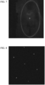
- the diffraction angle (Z-axis direction) of the laser light is constant on the screen, as shown in Fig. 7 , but in the X and Y directions, a ring-shaped bright line is projected, which indicates an isotropic crystal orientation. Therefore, it was confirmed that, with the method according to this working example, there is substantially no directionality of diffracted light.
- aqueous dispersion (dispersion) of 7.2% by mass spherical colloidal silica having an average particle size of 120.2 nm and a coefficient of variation of particle size of 6.5% was prepared. Note that the average particle size and coefficient of variation of particle size were determined from the peak obtained by fitting the particle size distribution determined by particle dynamic light scattering using a Zetasizer Nano-ZS (Malvern Instruments Ltd.) to a Gaussian curve.
- this dispersion was filtered with a membrane filter having a pore size of 0.45 ⁇ m, and then a hydrolysate aqueous solution of 0.8% by mass hexyltrimethoxysilane was added to the dispersion that had passed through the membrane filter, and this was reacted for 2 h at approximately 40°C.
- the dispersion and the hydrolysate aqueous solution were mixed such that the mass of phenyltriethoxysilane was 0.02 times the mass of colloidal silica particles.
- a spherically concaved stainless steel sheet (both-sided mirror-polished) having a radius of curvature of 45 mm and a diameter of 30 mm was prepared as a base material, and chromium (Cr) was sputtered to a thickness of 1.0 ⁇ m on the base material surface to form an inorganic film, and a workpiece was thereby obtained.
- the hydrophobized colloidal silica dispersion after oil phase extraction was dripped at a drip rate of 0.01 mL/s onto the liquid surface (using water as the lower-layer water having a temperature of 25°C) in a water tank (LB trough device) equipped with a surface pressure sensor for measuring surface pressure of the single-particle film and a movable barrier for compressing the single-particle film along the liquid surface.
- a water tank LB trough device
- ultrasonic waves having a power of 50 W and a frequency of 1,500 kHz
- ultrasonic waves having a power of 50 W and a frequency of 1,500 kHz
- this single-particle film was compressed by the movable barrier until the diffusion pressure reached 30 mNm -1 , and then the immersed workpiece was raised at a speed of 5 mm/min, and the single-particle film was thereby transferred onto the inorganic film of the workpiece.
- a hydrolysate solution of 1% by mass monomethyl trimethoxysilane was made to penetrate the workpiece on which the single-particle film had been formed, and then the excess hydrolysate solution was removed by treatment with a spin coater (3,000 rpm) for 1 min. After that, it was heated for 10 min at 100°C to cause the binder to react, and a workpiece with a single-particle film etching mask made of colloidal silica was obtained.
- One 10 ⁇ m ⁇ 10 ⁇ m region of the single-particle film etching mask was randomly selected, and an atomic force microscope image of that portion was obtained. Waveform separation of the image was performed by Fourier transform, and an FFT image was obtained. Next, the distance from the zero-order peak to the first-order peak in the profile of the FFT image was determined, and the reciprocal thereof was determined. The determined reciprocal is the modal pitch B 1 between particles in that region.
- This process was similarly performed for a 10 ⁇ m ⁇ 10 ⁇ m region in a total of 25 locations, the modal pitches B 1 to B 25 of the respective regions were determined, and the average thereof was calculated and used as the modal pitch B in formula (1). Note that at this time, the regions were set such that adjacent regions were approximately 5 mm apart from each other. The calculated modal pitch B was 121.8 nm.
- gas-phase etching using a mixed gas with a ratio of Cl 2 :O 2 :CHF 3 from 15:5:1 to 25:15:10 was performed on the workpiece with the single-particle film etching mask, so that fine recesses and protrusions were formed.
- the etching conditions included an antenna power of 1,500 W, a bias power of from 200 W to 800 W, and a gas flow rate of from 30 sccm to 50 sccm.
- the average height h of the fine recesses and protrusions actually measured from the atomic force microscope image was 330.4 nm
- the average pitch C (average diameter d of circular bottom) of the arrangement of the fine recesses and protrusions determined by the same method as that used for the single-particle film etching mask was 118.8 nm, and the aspect ratio calculated from these was 2.78.
- the divergence D' of the arrangement of these fine recesses and protrusions was determined using formula (2), it was 1.16%.
- the mold provided with a concave portion having fine recesses and protrusions produced in this manner was combined with a mold for a lens body part, and a space having a lens form was provided. Then, this mold was mounted on an injection molder, and acrylic resin (PMMA) having fluidity at high temperature was injected into the space and then cooled. A lens with a fine structure, which is a molding, was then removed. The face opposite the recessing and protruding structure face of this lens with a fine structure was flat.
- PMMA acrylic resin
- a mold was obtained by forming fine recesses and protrusions in a triangular lattice arrangement at a pitch of 460 nm and height of 200 nm on a silicon sheet (having a thickness of 0.3 mm, and a size of 30 mm ⁇ 30 mm) by interference exposure.
- the mold affixed to the stainless steel sheet was pressed with a pressure of 2.4 MPa against ultraviolet ray-curable resin (PAK-01CL manufactured by Toyo Gosei Co., Ltd.) applied on a pickup film (TETORON (registered trademark) film having a thickness of 50 ⁇ m manufactured by Teijin Ltd.) while the ultraviolet ray-curable resin was exposed with ultraviolet rays of 2.0 J and then cured. Then, the cured resin was gently peeled from the mold and then from the pickup film, and a nanoimprinted optical element of thickness approximately 1.0 mm was removed.
- PAK-01CL ultraviolet ray-curable resin
- TETORON registered trademark
- a spherically concaved stainless steel sheet (both-sided mirror-polished) having a radius of curvature of 45 mm and a diameter of 30 mm was prepared as a base material, and fine processing was performed by the particle mask method according to the same method as Working Example 2 except that no etching layer was provided, and a lens with a fine structure was obtained.
- the average height h of the fine recesses and protrusions was 18.6 nm
- the average pitch C (average diameter d of circular bottom) of the fine recesses and protrusions was 115.7 nm
- the aspect ratio calculated from these was 0.16.
- the visible light surface reflectance was approximately 5.2%.
Landscapes
- Engineering & Computer Science (AREA)
- Physics & Mathematics (AREA)
- Mechanical Engineering (AREA)
- General Physics & Mathematics (AREA)
- Optics & Photonics (AREA)
- Manufacturing & Machinery (AREA)
- Health & Medical Sciences (AREA)
- Ophthalmology & Optometry (AREA)
- Moulds For Moulding Plastics Or The Like (AREA)
- Shaping Of Tube Ends By Bending Or Straightening (AREA)
- Surface Treatment Of Optical Elements (AREA)
- Electroluminescent Light Sources (AREA)
Claims (5)
- Form (10) zur Herstellung eines optischen Elements, umfassend:ein Basismaterial (11); undeine vertiefende und vorragende Schicht (12), die auf einer Oberfläche des Basismaterials ausgebildet ist und eine vertiefende und vorragende Struktur (12a) aufweist;wobei die vertiefende und vorragende Struktur (12a) eine Vielzahl von Bereichen (C1 - Cn) aufweist, die kontinuierlich in einer Positionsbeziehung angeordnet ist, in welcher ein zentraler Punkt von sieben benachbarten Vorsprüngen ein Schnittpunkt von diagonalen Linien von sechs Eckpunkten eines gleichmäßigen Sechsecks ist und Bereiche, Formen und Kristallausrichtungen der Vielzahl von Bereichen zufällig sind,dadurch gekennzeichnet, dassdas Basismaterial (11) aus Edelstahl besteht unddie vertiefende und vorragende Schicht (12) durch ein Ti, Cr, W und Ni enthaltendes Material ausgebildet ist.
- Form (10) zur Herstellung eines optischen Elements nach Anspruch 1, wobei
die Oberfläche des Basismaterials (11) flach ist. - Form (10) zur Herstellung eines optischen Elements nach Anspruch 1, wobei
die Oberfläche des Basismaterials (11) eine von einer konkav gekrümmten Fläche und einer konvex gekrümmten Fläche aufweist. - Verfahren zum Fertigen einer Form (10) zur Herstellung eines optischen Elements, wobei das Verfahren die folgenden Schritte umfasst:einen Filmabscheidungsschritt zum Abscheiden eines anorganischen Films (12b) auf einer Oberfläche eines Basismaterials (11);einen Partikelanordnungsschritt zum Anordnen einer Vielzahl von Partikeln (M) in einer Monoschicht auf einer Oberfläche des anorganischen Films; undeinen Ätzschritt zum Trockenätzen des anorganischen Films (12b) unter Verwendung der Vielzahl von Partikeln (M) als Ätzmaske;dadurch gekennzeichnet, dassdas Basismaterial (11) aus Edelstahl besteht undder anorganische Film (12b) durch ein Ti, Cr, W und Ni enthaltendes Material ausgebildet ist.
- Verfahren zum Fertigen einer Form (10) zur Herstellung eines optischen Elements nach Anspruch 4, wobei
der Partikelanordnungsschritt einen Einzelpartikelfilmausbildungsschritt zum Ausbilden eines Einzelpartikelfilms auf einer Wasseroberfläche und einen Übertragungsschritt zum Übertragen des Einzelpartikelfilms auf die Oberfläche des anorganischen Films (12b) aufweist.
Applications Claiming Priority (2)
| Application Number | Priority Date | Filing Date | Title |
|---|---|---|---|
| JP2012272227 | 2012-12-13 | ||
| PCT/JP2013/083250 WO2014092132A1 (ja) | 2012-12-13 | 2013-12-11 | 光学素子作製用金型及びその製造方法、光学素子 |
Publications (3)
| Publication Number | Publication Date |
|---|---|
| EP2944446A1 EP2944446A1 (de) | 2015-11-18 |
| EP2944446A4 EP2944446A4 (de) | 2016-09-21 |
| EP2944446B1 true EP2944446B1 (de) | 2024-01-24 |
Family
ID=50934416
Family Applications (1)
| Application Number | Title | Priority Date | Filing Date |
|---|---|---|---|
| EP13862654.4A Active EP2944446B1 (de) | 2012-12-13 | 2013-12-11 | Form zur herstellung eines optischen elements und herstellungsverfahren dafür |
Country Status (7)
| Country | Link |
|---|---|
| US (1) | US9915758B2 (de) |
| EP (1) | EP2944446B1 (de) |
| JP (1) | JP6070720B2 (de) |
| KR (1) | KR20150067299A (de) |
| CN (1) | CN104781059B (de) |
| TW (1) | TWI604932B (de) |
| WO (1) | WO2014092132A1 (de) |
Families Citing this family (14)
| Publication number | Priority date | Publication date | Assignee | Title |
|---|---|---|---|---|
| JP6105490B2 (ja) * | 2012-01-27 | 2017-03-29 | 旭化成株式会社 | ドライエッチング用熱反応型レジスト材料、及びモールドの製造方法 |
| EP3211458B1 (de) * | 2014-10-24 | 2020-07-22 | Oji Holdings Corporation | Optisches element, optisches verbundelement und optisches verbundelement mit angehängter schutzfolie |
| JP6784487B2 (ja) | 2015-10-30 | 2020-11-11 | デクセリアルズ株式会社 | 光学体、および表示装置 |
| CN108439329A (zh) * | 2018-03-14 | 2018-08-24 | 河南科技大学 | 一种微纳模具型槽的制备方法 |
| TWI688464B (zh) * | 2018-11-14 | 2020-03-21 | 國立虎尾科技大學 | 仿生增亮膜、其製法及其應用的光學元件 |
| WO2020146318A1 (en) * | 2019-01-07 | 2020-07-16 | Glint Photonics, Inc. | Antireflective structures for light emitting diodes |
| US11968772B2 (en) * | 2019-05-30 | 2024-04-23 | Kla Corporation | Optical etendue matching methods for extreme ultraviolet metrology |
| EP4050911B1 (de) * | 2019-10-21 | 2025-06-25 | FUJIFILM Corporation | Akustische linse für ultraschallwandler, ultraschallwandler, ultraschallsonde und ultraschalldiagnosegerät |
| JP7343384B2 (ja) * | 2019-12-20 | 2023-09-12 | デクセリアルズ株式会社 | ロール金型製造方法、ロール金型製造装置およびプログラム |
| JP7491126B2 (ja) * | 2020-07-29 | 2024-05-28 | 東京エレクトロン株式会社 | 基板処理装置、及び基板処理方法。 |
| EP3964356A1 (de) * | 2020-09-03 | 2022-03-09 | Boegli-Gravures SA | Verfahren und vorrichtung zur herstellung einer prägevorrichtung unter verwendung einer ätzmaske |
| CN113023668B (zh) * | 2021-03-10 | 2022-10-04 | 北京理工大学 | 一种基于模板制造两级微纳结构阵列的方法 |
| JP2023176513A (ja) * | 2022-05-31 | 2023-12-13 | キヤノン株式会社 | 成形品および製造方法 |
| JP2025099348A (ja) * | 2023-12-21 | 2025-07-03 | デクセリアルズ株式会社 | 構造体、構造体モジュール、および構造体の製造方法 |
Family Cites Families (20)
| Publication number | Priority date | Publication date | Assignee | Title |
|---|---|---|---|---|
| JPH03252936A (ja) | 1990-02-28 | 1991-11-12 | Hitachi Chem Co Ltd | 光ディスク用スタンパ |
| JP2001121582A (ja) | 1999-10-26 | 2001-05-08 | Ntt Advanced Technology Corp | 金型およびその製造方法 |
| JP4218372B2 (ja) | 2003-03-06 | 2009-02-04 | コニカミノルタオプト株式会社 | 光学素子用金型の製造方法 |
| US8133538B2 (en) | 2006-03-17 | 2012-03-13 | Canon Kabushiki Kaisha | Method of producing mold having uneven structure |
| WO2008001670A1 (en) | 2006-06-30 | 2008-01-03 | Oji Paper Co., Ltd. | Monoparticulate-film etching mask and process for producing the same, process for producing fine structure with the monoparticulate-film etching mask, and fine structure obtained by the production process |
| JP5380803B2 (ja) * | 2007-08-03 | 2014-01-08 | 王子ホールディングス株式会社 | 非平面上単粒子膜の製造方法、該単粒子膜エッチングマスクを用いた微細構造体の製造方法および該製造方法で得られた微細構造体。 |
| JP2009128538A (ja) * | 2007-11-21 | 2009-06-11 | Panasonic Corp | 反射防止構造体の製造方法 |
| JP5157435B2 (ja) | 2007-12-28 | 2013-03-06 | 王子ホールディングス株式会社 | 凹凸パターンシートの製造方法、及び光学シートの製造方法 |
| JP4945460B2 (ja) | 2008-01-04 | 2012-06-06 | 株式会社東芝 | 反射防止構造の形成方法および反射防止構造 |
| JP2009175401A (ja) * | 2008-01-24 | 2009-08-06 | Oji Paper Co Ltd | 視野角制御機能を有する周期格子構造 |
| JP5237658B2 (ja) | 2008-03-18 | 2013-07-17 | ペンタックスリコーイメージング株式会社 | 基板上に規則的に二次元配置した構造体、及びその形成方法 |
| JP2009292703A (ja) | 2008-06-09 | 2009-12-17 | Hitachi Maxell Ltd | 光学素子成形用の金型の製造方法および光学素子の製造方法 |
| WO2010125795A1 (ja) * | 2009-04-30 | 2010-11-04 | シャープ株式会社 | 型およびその製造方法 |
| JP5175812B2 (ja) * | 2009-08-04 | 2013-04-03 | 株式会社Bmg | ナノ金型、金型の製造方法および磁気記録媒体の製造方法 |
| JP2011186414A (ja) * | 2010-02-12 | 2011-09-22 | Sony Corp | 光学素子、日射遮蔽装置、建具、窓材および光学素子の製造方法 |
| JP2012020389A (ja) | 2010-07-16 | 2012-02-02 | Oji Paper Co Ltd | 単粒子膜被覆ロールの製造方法、凹凸形成ロールの製造方法、凹凸形成フィルムの製造方法および単粒子膜被覆装置 |
| JP2012028067A (ja) * | 2010-07-21 | 2012-02-09 | Oji Paper Co Ltd | 有機発光ダイオード素子、画像表示装置及び照明装置 |
| KR101340845B1 (ko) * | 2011-01-13 | 2013-12-13 | 한국기계연구원 | 기능성 표면의 제조방법 |
| JP2012183753A (ja) | 2011-03-07 | 2012-09-27 | Fujifilm Corp | ナノインプリント方法 |
| JP5615971B2 (ja) * | 2011-04-01 | 2014-10-29 | シャープ株式会社 | 型の製造方法 |
-
2013
- 2013-12-11 JP JP2014552072A patent/JP6070720B2/ja active Active
- 2013-12-11 WO PCT/JP2013/083250 patent/WO2014092132A1/ja not_active Ceased
- 2013-12-11 US US14/647,974 patent/US9915758B2/en active Active
- 2013-12-11 EP EP13862654.4A patent/EP2944446B1/de active Active
- 2013-12-11 CN CN201380059083.5A patent/CN104781059B/zh active Active
- 2013-12-11 KR KR1020157011779A patent/KR20150067299A/ko not_active Ceased
- 2013-12-13 TW TW102146249A patent/TWI604932B/zh active
Also Published As
| Publication number | Publication date |
|---|---|
| JPWO2014092132A1 (ja) | 2017-01-12 |
| US20150301230A1 (en) | 2015-10-22 |
| KR20150067299A (ko) | 2015-06-17 |
| CN104781059A (zh) | 2015-07-15 |
| US9915758B2 (en) | 2018-03-13 |
| CN104781059B (zh) | 2017-05-10 |
| TW201431660A (zh) | 2014-08-16 |
| JP6070720B2 (ja) | 2017-02-01 |
| EP2944446A1 (de) | 2015-11-18 |
| EP2944446A4 (de) | 2016-09-21 |
| WO2014092132A1 (ja) | 2014-06-19 |
| TWI604932B (zh) | 2017-11-11 |
Similar Documents
| Publication | Publication Date | Title |
|---|---|---|
| EP2944446B1 (de) | Form zur herstellung eines optischen elements und herstellungsverfahren dafür | |
| JP5359270B2 (ja) | 単粒子膜エッチングマスクを用いた微細構造体の製造方法およびナノインプリント用または射出成型用モールドの製造方法 | |
| JP5380803B2 (ja) | 非平面上単粒子膜の製造方法、該単粒子膜エッチングマスクを用いた微細構造体の製造方法および該製造方法で得られた微細構造体。 | |
| EP2065736B1 (de) | Antireflexstrukturkörper, verfahren zu seiner herstellung und verfahren zur herstellung eines optischen bauteils | |
| JP2009162831A (ja) | 凹凸パターンシート及びその製造方法、光学シートの製造方法、並びに光学装置 | |
| JP5141506B2 (ja) | プラズモニック結晶面発光体、画像表示装置及び照明装置 | |
| JP5130481B2 (ja) | 透明材料付半導体発光素子 | |
| JP5423758B2 (ja) | 単粒子膜および微細構造体 | |
| JP2012028067A (ja) | 有機発光ダイオード素子、画像表示装置及び照明装置 | |
| JP2013083997A (ja) | 凹凸パターンシート、及び光学装置 | |
| JP5915696B2 (ja) | 単粒子膜エッチングマスク付基板の製造方法 | |
| JP2014081656A (ja) | 光学シートとその原版、及び光学装置 | |
| WO2014163041A1 (ja) | 転写フィルムおよび凹凸構造付基板 | |
| JP5987894B2 (ja) | 凹凸パターンシートの製造方法、及び光学シートの製造方法 | |
| JP2009175401A (ja) | 視野角制御機能を有する周期格子構造 | |
| KR101769183B1 (ko) | 금속층을 포함하는 전도성 필름의 제조방법 및 이를 이용하여 제조된 전도성 필름 | |
| JP2013210678A (ja) | 非平面上単粒子膜の製造方法、該単粒子膜エッチングマスクを用いた微細構造体の製造方法および該製造方法で得られた微細構造体。 |
Legal Events
| Date | Code | Title | Description |
|---|---|---|---|
| PUAI | Public reference made under article 153(3) epc to a published international application that has entered the european phase |
Free format text: ORIGINAL CODE: 0009012 |
|
| 17P | Request for examination filed |
Effective date: 20150602 |
|
| AK | Designated contracting states |
Kind code of ref document: A1 Designated state(s): AL AT BE BG CH CY CZ DE DK EE ES FI FR GB GR HR HU IE IS IT LI LT LU LV MC MK MT NL NO PL PT RO RS SE SI SK SM TR |
|
| AX | Request for extension of the european patent |
Extension state: BA ME |
|
| DAX | Request for extension of the european patent (deleted) | ||
| A4 | Supplementary search report drawn up and despatched |
Effective date: 20160819 |
|
| RIC1 | Information provided on ipc code assigned before grant |
Ipc: H05B 33/02 20060101ALI20160815BHEP Ipc: B29C 59/02 20060101ALI20160815BHEP Ipc: B29D 11/00 20060101ALI20160815BHEP Ipc: H01L 51/50 20060101ALI20160815BHEP Ipc: H01L 21/027 20060101ALI20160815BHEP Ipc: B29C 33/38 20060101AFI20160815BHEP Ipc: B29C 33/42 20060101ALI20160815BHEP Ipc: G02B 1/11 20150101ALI20160815BHEP Ipc: G02B 5/18 20060101ALI20160815BHEP |
|
| STAA | Information on the status of an ep patent application or granted ep patent |
Free format text: STATUS: EXAMINATION IS IN PROGRESS |
|
| 17Q | First examination report despatched |
Effective date: 20201105 |
|
| RIC1 | Information provided on ipc code assigned before grant |
Ipc: B29C 37/00 20060101ALI20220818BHEP Ipc: G02B 1/118 20150101ALI20220818BHEP Ipc: G02B 1/10 20150101ALI20220818BHEP Ipc: B29L 11/00 20060101ALI20220818BHEP Ipc: B29C 33/42 20060101ALI20220818BHEP Ipc: B29C 59/02 20060101ALI20220818BHEP Ipc: G02B 1/11 20150101ALI20220818BHEP Ipc: G02B 5/18 20060101ALI20220818BHEP Ipc: H01L 21/027 20060101ALI20220818BHEP Ipc: H01L 51/50 20060101ALI20220818BHEP Ipc: H05B 33/02 20060101ALI20220818BHEP Ipc: B29D 11/00 20060101ALI20220818BHEP Ipc: B29C 33/38 20060101AFI20220818BHEP |
|
| RIC1 | Information provided on ipc code assigned before grant |
Ipc: B29L 11/00 20060101ALN20230721BHEP Ipc: B29C 37/00 20060101ALI20230721BHEP Ipc: G02B 1/118 20150101ALI20230721BHEP Ipc: G02B 1/10 20150101ALI20230721BHEP Ipc: B29C 33/42 20060101ALI20230721BHEP Ipc: B29C 59/02 20060101ALI20230721BHEP Ipc: G02B 1/11 20150101ALI20230721BHEP Ipc: G02B 5/18 20060101ALI20230721BHEP Ipc: H01L 21/027 20060101ALI20230721BHEP Ipc: H05B 33/02 20060101ALI20230721BHEP Ipc: B29D 11/00 20060101ALI20230721BHEP Ipc: B29C 33/38 20060101AFI20230721BHEP |
|
| GRAP | Despatch of communication of intention to grant a patent |
Free format text: ORIGINAL CODE: EPIDOSNIGR1 |
|
| STAA | Information on the status of an ep patent application or granted ep patent |
Free format text: STATUS: GRANT OF PATENT IS INTENDED |
|
| RIC1 | Information provided on ipc code assigned before grant |
Ipc: B29L 11/00 20060101ALN20230818BHEP Ipc: B29C 37/00 20060101ALI20230818BHEP Ipc: G02B 1/118 20150101ALI20230818BHEP Ipc: G02B 1/10 20150101ALI20230818BHEP Ipc: B29C 33/42 20060101ALI20230818BHEP Ipc: B29C 59/02 20060101ALI20230818BHEP Ipc: G02B 1/11 20150101ALI20230818BHEP Ipc: G02B 5/18 20060101ALI20230818BHEP Ipc: H01L 21/027 20060101ALI20230818BHEP Ipc: H05B 33/02 20060101ALI20230818BHEP Ipc: B29D 11/00 20060101ALI20230818BHEP Ipc: B29C 33/38 20060101AFI20230818BHEP |
|
| INTG | Intention to grant announced |
Effective date: 20230913 |
|
| GRAS | Grant fee paid |
Free format text: ORIGINAL CODE: EPIDOSNIGR3 |
|
| GRAA | (expected) grant |
Free format text: ORIGINAL CODE: 0009210 |
|
| STAA | Information on the status of an ep patent application or granted ep patent |
Free format text: STATUS: THE PATENT HAS BEEN GRANTED |
|
| AK | Designated contracting states |
Kind code of ref document: B1 Designated state(s): AL AT BE BG CH CY CZ DE DK EE ES FI FR GB GR HR HU IE IS IT LI LT LU LV MC MK MT NL NO PL PT RO RS SE SI SK SM TR |
|
| P01 | Opt-out of the competence of the unified patent court (upc) registered |
Effective date: 20231214 |
|
| REG | Reference to a national code |
Ref country code: GB Ref legal event code: FG4D |
|
| REG | Reference to a national code |
Ref country code: CH Ref legal event code: EP |
|
| REG | Reference to a national code |
Ref country code: IE Ref legal event code: FG4D |
|
| REG | Reference to a national code |
Ref country code: DE Ref legal event code: R096 Ref document number: 602013085239 Country of ref document: DE |
|
| REG | Reference to a national code |
Ref country code: LT Ref legal event code: MG9D |
|
| REG | Reference to a national code |
Ref country code: NL Ref legal event code: MP Effective date: 20240124 |
|
| PG25 | Lapsed in a contracting state [announced via postgrant information from national office to epo] |
Ref country code: NL Free format text: LAPSE BECAUSE OF FAILURE TO SUBMIT A TRANSLATION OF THE DESCRIPTION OR TO PAY THE FEE WITHIN THE PRESCRIBED TIME-LIMIT Effective date: 20240124 |
|
| PG25 | Lapsed in a contracting state [announced via postgrant information from national office to epo] |
Ref country code: NL Free format text: LAPSE BECAUSE OF FAILURE TO SUBMIT A TRANSLATION OF THE DESCRIPTION OR TO PAY THE FEE WITHIN THE PRESCRIBED TIME-LIMIT Effective date: 20240124 |
|
| PG25 | Lapsed in a contracting state [announced via postgrant information from national office to epo] |
Ref country code: IS Free format text: LAPSE BECAUSE OF FAILURE TO SUBMIT A TRANSLATION OF THE DESCRIPTION OR TO PAY THE FEE WITHIN THE PRESCRIBED TIME-LIMIT Effective date: 20240524 |
|
| PG25 | Lapsed in a contracting state [announced via postgrant information from national office to epo] |
Ref country code: LT Free format text: LAPSE BECAUSE OF FAILURE TO SUBMIT A TRANSLATION OF THE DESCRIPTION OR TO PAY THE FEE WITHIN THE PRESCRIBED TIME-LIMIT Effective date: 20240124 |
|
| PG25 | Lapsed in a contracting state [announced via postgrant information from national office to epo] |
Ref country code: GR Free format text: LAPSE BECAUSE OF FAILURE TO SUBMIT A TRANSLATION OF THE DESCRIPTION OR TO PAY THE FEE WITHIN THE PRESCRIBED TIME-LIMIT Effective date: 20240425 |
|
| REG | Reference to a national code |
Ref country code: AT Ref legal event code: MK05 Ref document number: 1651842 Country of ref document: AT Kind code of ref document: T Effective date: 20240124 |
|
| PG25 | Lapsed in a contracting state [announced via postgrant information from national office to epo] |
Ref country code: RS Free format text: LAPSE BECAUSE OF FAILURE TO SUBMIT A TRANSLATION OF THE DESCRIPTION OR TO PAY THE FEE WITHIN THE PRESCRIBED TIME-LIMIT Effective date: 20240424 Ref country code: HR Free format text: LAPSE BECAUSE OF FAILURE TO SUBMIT A TRANSLATION OF THE DESCRIPTION OR TO PAY THE FEE WITHIN THE PRESCRIBED TIME-LIMIT Effective date: 20240124 |
|
| PG25 | Lapsed in a contracting state [announced via postgrant information from national office to epo] |
Ref country code: ES Free format text: LAPSE BECAUSE OF FAILURE TO SUBMIT A TRANSLATION OF THE DESCRIPTION OR TO PAY THE FEE WITHIN THE PRESCRIBED TIME-LIMIT Effective date: 20240124 |
|
| PG25 | Lapsed in a contracting state [announced via postgrant information from national office to epo] |
Ref country code: AT Free format text: LAPSE BECAUSE OF FAILURE TO SUBMIT A TRANSLATION OF THE DESCRIPTION OR TO PAY THE FEE WITHIN THE PRESCRIBED TIME-LIMIT Effective date: 20240124 |
|
| PG25 | Lapsed in a contracting state [announced via postgrant information from national office to epo] |
Ref country code: RS Free format text: LAPSE BECAUSE OF FAILURE TO SUBMIT A TRANSLATION OF THE DESCRIPTION OR TO PAY THE FEE WITHIN THE PRESCRIBED TIME-LIMIT Effective date: 20240424 Ref country code: NO Free format text: LAPSE BECAUSE OF FAILURE TO SUBMIT A TRANSLATION OF THE DESCRIPTION OR TO PAY THE FEE WITHIN THE PRESCRIBED TIME-LIMIT Effective date: 20240424 Ref country code: LT Free format text: LAPSE BECAUSE OF FAILURE TO SUBMIT A TRANSLATION OF THE DESCRIPTION OR TO PAY THE FEE WITHIN THE PRESCRIBED TIME-LIMIT Effective date: 20240124 Ref country code: IS Free format text: LAPSE BECAUSE OF FAILURE TO SUBMIT A TRANSLATION OF THE DESCRIPTION OR TO PAY THE FEE WITHIN THE PRESCRIBED TIME-LIMIT Effective date: 20240524 Ref country code: HR Free format text: LAPSE BECAUSE OF FAILURE TO SUBMIT A TRANSLATION OF THE DESCRIPTION OR TO PAY THE FEE WITHIN THE PRESCRIBED TIME-LIMIT Effective date: 20240124 Ref country code: GR Free format text: LAPSE BECAUSE OF FAILURE TO SUBMIT A TRANSLATION OF THE DESCRIPTION OR TO PAY THE FEE WITHIN THE PRESCRIBED TIME-LIMIT Effective date: 20240425 Ref country code: FI Free format text: LAPSE BECAUSE OF FAILURE TO SUBMIT A TRANSLATION OF THE DESCRIPTION OR TO PAY THE FEE WITHIN THE PRESCRIBED TIME-LIMIT Effective date: 20240124 Ref country code: ES Free format text: LAPSE BECAUSE OF FAILURE TO SUBMIT A TRANSLATION OF THE DESCRIPTION OR TO PAY THE FEE WITHIN THE PRESCRIBED TIME-LIMIT Effective date: 20240124 Ref country code: BG Free format text: LAPSE BECAUSE OF FAILURE TO SUBMIT A TRANSLATION OF THE DESCRIPTION OR TO PAY THE FEE WITHIN THE PRESCRIBED TIME-LIMIT Effective date: 20240124 Ref country code: AT Free format text: LAPSE BECAUSE OF FAILURE TO SUBMIT A TRANSLATION OF THE DESCRIPTION OR TO PAY THE FEE WITHIN THE PRESCRIBED TIME-LIMIT Effective date: 20240124 |
|
| PG25 | Lapsed in a contracting state [announced via postgrant information from national office to epo] |
Ref country code: PT Free format text: LAPSE BECAUSE OF FAILURE TO SUBMIT A TRANSLATION OF THE DESCRIPTION OR TO PAY THE FEE WITHIN THE PRESCRIBED TIME-LIMIT Effective date: 20240524 Ref country code: PL Free format text: LAPSE BECAUSE OF FAILURE TO SUBMIT A TRANSLATION OF THE DESCRIPTION OR TO PAY THE FEE WITHIN THE PRESCRIBED TIME-LIMIT Effective date: 20240124 |
|
| PG25 | Lapsed in a contracting state [announced via postgrant information from national office to epo] |
Ref country code: SE Free format text: LAPSE BECAUSE OF FAILURE TO SUBMIT A TRANSLATION OF THE DESCRIPTION OR TO PAY THE FEE WITHIN THE PRESCRIBED TIME-LIMIT Effective date: 20240124 Ref country code: PT Free format text: LAPSE BECAUSE OF FAILURE TO SUBMIT A TRANSLATION OF THE DESCRIPTION OR TO PAY THE FEE WITHIN THE PRESCRIBED TIME-LIMIT Effective date: 20240524 Ref country code: PL Free format text: LAPSE BECAUSE OF FAILURE TO SUBMIT A TRANSLATION OF THE DESCRIPTION OR TO PAY THE FEE WITHIN THE PRESCRIBED TIME-LIMIT Effective date: 20240124 Ref country code: LV Free format text: LAPSE BECAUSE OF FAILURE TO SUBMIT A TRANSLATION OF THE DESCRIPTION OR TO PAY THE FEE WITHIN THE PRESCRIBED TIME-LIMIT Effective date: 20240124 |
|
| PG25 | Lapsed in a contracting state [announced via postgrant information from national office to epo] |
Ref country code: DK Free format text: LAPSE BECAUSE OF FAILURE TO SUBMIT A TRANSLATION OF THE DESCRIPTION OR TO PAY THE FEE WITHIN THE PRESCRIBED TIME-LIMIT Effective date: 20240124 |
|
| PG25 | Lapsed in a contracting state [announced via postgrant information from national office to epo] |
Ref country code: SM Free format text: LAPSE BECAUSE OF FAILURE TO SUBMIT A TRANSLATION OF THE DESCRIPTION OR TO PAY THE FEE WITHIN THE PRESCRIBED TIME-LIMIT Effective date: 20240124 |
|
| PG25 | Lapsed in a contracting state [announced via postgrant information from national office to epo] |
Ref country code: EE Free format text: LAPSE BECAUSE OF FAILURE TO SUBMIT A TRANSLATION OF THE DESCRIPTION OR TO PAY THE FEE WITHIN THE PRESCRIBED TIME-LIMIT Effective date: 20240124 Ref country code: CZ Free format text: LAPSE BECAUSE OF FAILURE TO SUBMIT A TRANSLATION OF THE DESCRIPTION OR TO PAY THE FEE WITHIN THE PRESCRIBED TIME-LIMIT Effective date: 20240124 |
|
| REG | Reference to a national code |
Ref country code: DE Ref legal event code: R097 Ref document number: 602013085239 Country of ref document: DE |
|
| PG25 | Lapsed in a contracting state [announced via postgrant information from national office to epo] |
Ref country code: SK Free format text: LAPSE BECAUSE OF FAILURE TO SUBMIT A TRANSLATION OF THE DESCRIPTION OR TO PAY THE FEE WITHIN THE PRESCRIBED TIME-LIMIT Effective date: 20240124 |
|
| PG25 | Lapsed in a contracting state [announced via postgrant information from national office to epo] |
Ref country code: SM Free format text: LAPSE BECAUSE OF FAILURE TO SUBMIT A TRANSLATION OF THE DESCRIPTION OR TO PAY THE FEE WITHIN THE PRESCRIBED TIME-LIMIT Effective date: 20240124 Ref country code: SK Free format text: LAPSE BECAUSE OF FAILURE TO SUBMIT A TRANSLATION OF THE DESCRIPTION OR TO PAY THE FEE WITHIN THE PRESCRIBED TIME-LIMIT Effective date: 20240124 Ref country code: RO Free format text: LAPSE BECAUSE OF FAILURE TO SUBMIT A TRANSLATION OF THE DESCRIPTION OR TO PAY THE FEE WITHIN THE PRESCRIBED TIME-LIMIT Effective date: 20240124 Ref country code: EE Free format text: LAPSE BECAUSE OF FAILURE TO SUBMIT A TRANSLATION OF THE DESCRIPTION OR TO PAY THE FEE WITHIN THE PRESCRIBED TIME-LIMIT Effective date: 20240124 Ref country code: DK Free format text: LAPSE BECAUSE OF FAILURE TO SUBMIT A TRANSLATION OF THE DESCRIPTION OR TO PAY THE FEE WITHIN THE PRESCRIBED TIME-LIMIT Effective date: 20240124 Ref country code: CZ Free format text: LAPSE BECAUSE OF FAILURE TO SUBMIT A TRANSLATION OF THE DESCRIPTION OR TO PAY THE FEE WITHIN THE PRESCRIBED TIME-LIMIT Effective date: 20240124 |
|
| PLBE | No opposition filed within time limit |
Free format text: ORIGINAL CODE: 0009261 |
|
| STAA | Information on the status of an ep patent application or granted ep patent |
Free format text: STATUS: NO OPPOSITION FILED WITHIN TIME LIMIT |
|
| PG25 | Lapsed in a contracting state [announced via postgrant information from national office to epo] |
Ref country code: IT Free format text: LAPSE BECAUSE OF FAILURE TO SUBMIT A TRANSLATION OF THE DESCRIPTION OR TO PAY THE FEE WITHIN THE PRESCRIBED TIME-LIMIT Effective date: 20240124 |
|
| PG25 | Lapsed in a contracting state [announced via postgrant information from national office to epo] |
Ref country code: IT Free format text: LAPSE BECAUSE OF FAILURE TO SUBMIT A TRANSLATION OF THE DESCRIPTION OR TO PAY THE FEE WITHIN THE PRESCRIBED TIME-LIMIT Effective date: 20240124 |
|
| 26N | No opposition filed |
Effective date: 20241025 |
|
| PG25 | Lapsed in a contracting state [announced via postgrant information from national office to epo] |
Ref country code: SI Free format text: LAPSE BECAUSE OF FAILURE TO SUBMIT A TRANSLATION OF THE DESCRIPTION OR TO PAY THE FEE WITHIN THE PRESCRIBED TIME-LIMIT Effective date: 20240124 |
|
| PG25 | Lapsed in a contracting state [announced via postgrant information from national office to epo] |
Ref country code: MC Free format text: LAPSE BECAUSE OF FAILURE TO SUBMIT A TRANSLATION OF THE DESCRIPTION OR TO PAY THE FEE WITHIN THE PRESCRIBED TIME-LIMIT Effective date: 20240124 |
|
| REG | Reference to a national code |
Ref country code: CH Ref legal event code: PL |
|
| PG25 | Lapsed in a contracting state [announced via postgrant information from national office to epo] |
Ref country code: LU Free format text: LAPSE BECAUSE OF NON-PAYMENT OF DUE FEES Effective date: 20241211 |
|
| REG | Reference to a national code |
Ref country code: BE Ref legal event code: MM Effective date: 20241231 |
|
| PG25 | Lapsed in a contracting state [announced via postgrant information from national office to epo] |
Ref country code: BE Free format text: LAPSE BECAUSE OF NON-PAYMENT OF DUE FEES Effective date: 20241231 |
|
| PG25 | Lapsed in a contracting state [announced via postgrant information from national office to epo] |
Ref country code: CH Free format text: LAPSE BECAUSE OF NON-PAYMENT OF DUE FEES Effective date: 20241231 |
|
| PG25 | Lapsed in a contracting state [announced via postgrant information from national office to epo] |
Ref country code: IE Free format text: LAPSE BECAUSE OF NON-PAYMENT OF DUE FEES Effective date: 20241211 |
|
| PGFP | Annual fee paid to national office [announced via postgrant information from national office to epo] |
Ref country code: DE Payment date: 20251028 Year of fee payment: 13 |
|
| PGFP | Annual fee paid to national office [announced via postgrant information from national office to epo] |
Ref country code: GB Payment date: 20251030 Year of fee payment: 13 |
|
| PGFP | Annual fee paid to national office [announced via postgrant information from national office to epo] |
Ref country code: FR Payment date: 20251110 Year of fee payment: 13 |