EP2932218B1 - Sensor mit einem substrat. - Google Patents
Sensor mit einem substrat. Download PDFInfo
- Publication number
- EP2932218B1 EP2932218B1 EP13798922.4A EP13798922A EP2932218B1 EP 2932218 B1 EP2932218 B1 EP 2932218B1 EP 13798922 A EP13798922 A EP 13798922A EP 2932218 B1 EP2932218 B1 EP 2932218B1
- Authority
- EP
- European Patent Office
- Prior art keywords
- voltage
- substrate
- sensor
- wheatstone bridge
- supplied
- Prior art date
- Legal status (The legal status is an assumption and is not a legal conclusion. Google has not performed a legal analysis and makes no representation as to the accuracy of the status listed.)
- Active
Links
Images

Classifications
-
- G—PHYSICS
- G01—MEASURING; TESTING
- G01R—MEASURING ELECTRIC VARIABLES; MEASURING MAGNETIC VARIABLES
- G01R17/00—Measuring arrangements involving comparison with a reference value, e.g. bridge
- G01R17/10—AC or DC measuring bridges
-
- G—PHYSICS
- G01—MEASURING; TESTING
- G01L—MEASURING FORCE, STRESS, TORQUE, WORK, MECHANICAL POWER, MECHANICAL EFFICIENCY, OR FLUID PRESSURE
- G01L9/00—Measuring steady of quasi-steady pressure of fluid or fluent solid material by electric or magnetic pressure-sensitive elements; Transmitting or indicating the displacement of mechanical pressure-sensitive elements, used to measure the steady or quasi-steady pressure of a fluid or fluent solid material, by electric or magnetic means
- G01L9/02—Measuring steady of quasi-steady pressure of fluid or fluent solid material by electric or magnetic pressure-sensitive elements; Transmitting or indicating the displacement of mechanical pressure-sensitive elements, used to measure the steady or quasi-steady pressure of a fluid or fluent solid material, by electric or magnetic means by making use of variations in ohmic resistance, e.g. of potentiometers, electric circuits therefor, e.g. bridges, amplifiers or signal conditioning
- G01L9/06—Measuring steady of quasi-steady pressure of fluid or fluent solid material by electric or magnetic pressure-sensitive elements; Transmitting or indicating the displacement of mechanical pressure-sensitive elements, used to measure the steady or quasi-steady pressure of a fluid or fluent solid material, by electric or magnetic means by making use of variations in ohmic resistance, e.g. of potentiometers, electric circuits therefor, e.g. bridges, amplifiers or signal conditioning of piezo-resistive devices
-
- G—PHYSICS
- G01—MEASURING; TESTING
- G01L—MEASURING FORCE, STRESS, TORQUE, WORK, MECHANICAL POWER, MECHANICAL EFFICIENCY, OR FLUID PRESSURE
- G01L1/00—Measuring force or stress, in general
- G01L1/18—Measuring force or stress, in general using properties of piezo-resistive materials, i.e. materials of which the ohmic resistance varies according to changes in magnitude or direction of force applied to the material
-
- G—PHYSICS
- G01—MEASURING; TESTING
- G01L—MEASURING FORCE, STRESS, TORQUE, WORK, MECHANICAL POWER, MECHANICAL EFFICIENCY, OR FLUID PRESSURE
- G01L1/00—Measuring force or stress, in general
- G01L1/20—Measuring force or stress, in general by measuring variations in ohmic resistance of solid materials or of electrically-conductive fluids; by making use of electrokinetic cells, i.e. liquid-containing cells wherein an electrical potential is produced or varied upon the application of stress
- G01L1/22—Measuring force or stress, in general by measuring variations in ohmic resistance of solid materials or of electrically-conductive fluids; by making use of electrokinetic cells, i.e. liquid-containing cells wherein an electrical potential is produced or varied upon the application of stress using resistance strain gauges
- G01L1/225—Measuring circuits therefor
- G01L1/2262—Measuring circuits therefor involving simple electrical bridges
-
- G—PHYSICS
- G01—MEASURING; TESTING
- G01L—MEASURING FORCE, STRESS, TORQUE, WORK, MECHANICAL POWER, MECHANICAL EFFICIENCY, OR FLUID PRESSURE
- G01L9/00—Measuring steady of quasi-steady pressure of fluid or fluent solid material by electric or magnetic pressure-sensitive elements; Transmitting or indicating the displacement of mechanical pressure-sensitive elements, used to measure the steady or quasi-steady pressure of a fluid or fluent solid material, by electric or magnetic means
- G01L9/0041—Transmitting or indicating the displacement of flexible diaphragms
- G01L9/0051—Transmitting or indicating the displacement of flexible diaphragms using variations in ohmic resistance
- G01L9/0052—Transmitting or indicating the displacement of flexible diaphragms using variations in ohmic resistance of piezoresistive elements
- G01L9/0054—Transmitting or indicating the displacement of flexible diaphragms using variations in ohmic resistance of piezoresistive elements integral with a semiconducting diaphragm
Definitions
- the present invention relates to a sensor, such as a pressure sensor, comprising a substrate having measuring electronics including a Wheatstone bridge arranged thereon.
- US 6,933,582 discloses a semiconductor sensor including a p-type semiconductor substrate having an n-type semiconductor layer disposed on one surface of the substrate and a p-type diffused resistor disposed in the n-type semiconductor layer. A first electric voltage is applied to the n-type semiconductor layer, a second electric voltage is applied to the substrate, a third electric voltage is applied to the p-type diffused resistor. The first electric voltage is higher than the second and third electric voltages.
- the sensor ensures stable operation against electric leakage and high noise protection because two depletion layers are formed.
- US 5,681,997 discloses a polycrystalline pressure sensor formed by depositing polycrystalline silicon piezo resistors on a polycrystalline sensing diaphragm.
- the piezo resistors are arranged in a Wheatstone bridge configuration.
- an alternating differential signal is applied across the input of the Wheatstone bridge.
- a measured voltage difference between the output terminals of the Wheatstone bridge is used to detect imbalance in the electrical piezo resistors that corresponds to pressure applied to the sensor.
- US2006/0278012 discloses a shield film on top of an oxide film, which covers a substrate comprising a bridge circuit.
- EMI electromagnetic interference
- the invention provides a sensor comprising:
- the invention provides a sensor comprising:
- the sensor comprises a substrate.
- the substrate is an n-dosed substrate, and according to the second aspect of the invention, the substrate is a p-dosed substrate.
- the substrate may, e.g., be made from a semiconductor material, such as silicon, germanium, gallium arsenide, silicon carbide, etc.
- the sensor further comprises measuring electronics arranged at least partly on the substrate.
- all of the measuring electronics may be arranged on the substrate.
- some parts or components of the measuring electronics may be arranged on the substrate, while other parts or components of the measuring electronics may be arranged in other parts of the sensor, and/or arranged outside the sensor and simply connected to the parts or components of the measuring electronics which are arranged on the substrate.
- the measuring electronics comprises a Wheatstone bridge.
- the Wheatstone bridge is preferably arranged on the substrate.
- the Wheatstone bridge provides the actual measuring performed by the sensor. This will be described in further detail below.
- the sensor further comprises a field shield arranged on the substrate in such a manner that the field shield covers the Wheatstone bridge.
- the field shield thereby provides shielding for the Wheatstone bridge against external electromagnetic fields which could potentially disturb the measurements performed by means of the Wheatstone bridge.
- the field shield is preferably made from a metal, such as aluminium.
- the senor comprises a power supply arranged to supply electrical voltage to the substrate and the measuring electronics, in particular to the Wheatstone bridge.
- the power supply supplies a quasi-DC voltage to the Wheatstone bridge.
- the term 'quasi-DC voltage' should be interpreted to mean a voltage signal which is alternatingly switched between an upper voltage level and a lower voltage level, in such a manner that the upper voltage level is supplied to one node of the Wheatstone bridge when the lower voltage level is supplied to another node of the Wheatstone bridge, and vice versa.
- the voltage levels are reversed, so that the voltage level supplied to one node is switched from the upper level to the lower level, while the voltage level supplied to the another node is switched from the lower level to the upper level, etc.
- the power supply supplies a DC voltage to the substrate.
- the level of the DC voltage supplied to the substrate is higher than or equal to the quasi-DC voltage supplied to the Wheatstone bridge.
- the sensor is a sensor according to the second aspect of the invention, i.e. in the case that the substrate is a p-dosed substrate, the level of the DC voltage supplied to the substrate is lower than or equal to the quasi-DC voltage supplied to the Wheatstone bridge.
- the power supply may further be arranged to supply a voltage to the field shield.
- the sensor is a sensor according to the first aspect of the invention, i.e. in the case that the substrate is an n-dosed substrate
- the level of the voltage supplied to the field shield is higher than or equal to the quasi-DC voltage supplied to the Wheatstone bridge.
- the sensor is a sensor according to the second aspect of the invention, i.e. in the case that the substrate is a p-dosed substrate
- the level of the voltage supplied to the field shield is lower than or equal to the quasi-DC voltage supplied to the Wheatstone bridge.
- a voltage difference exists between the voltage supplied to the field shield, and either the voltage supplied to the Wheatstone bridge or the voltage supplied to the substrate.
- the level of the DC voltage supplied to the substrate may be equal to the level of the voltage supplied to the field shield. This may, e.g., be obtained by providing a direct electrical connection between the field shield and the substrate. According to this embodiment, the voltage supplied to the field shield is a DC voltage.
- the voltage supplied to the field shield may follow the 'quasi-DC voltage supplied to the Wheatstone bridge. This may, e.g., be obtained by providing a direct electrical connection between the field shield and the Wheatstone bridge. According to this embodiment, the voltage supplied to the field shield is a quasi-DC voltage.
- the difference between the DC voltage level supplied to the substrate and the quasi-DC voltage supplied to the Wheatstone bridge may be at least 0.5 V, such as at least 1.0 V, such as at least 3.0 V, such as at least 5.0 V, such as at least 7.0 V, such as at least 10.0 V.
- This is an advantage, because a large difference between the voltage levels minimises the capacitance between the four nodes of the Wheatstone bridge and a casing or chassis of the sensor.
- electron leakage and diffusion which would be a problem at large voltage differences in the case that a DC voltage was supplied to the Wheatstone bridge as well as to the substrate, is minimised due to the quasi-DC voltage supplied to the Wheatstone bridge.
- the measuring electronics may further comprise one or more resistors, each resistor being electrically connected between the power supply and an excitation node of the Wheatstone bridge.
- the voltage drop provided by the resistors bias the diodes of the Wheatstone bridge in the reverse direction.
- the sensor is a sensor according to the first aspect of the invention, i.e. in the case that the substrate is an n-dosed substrate, this reduces the voltage level supplied by the power supply, and the 'quasi-DC voltage level supplied to the Wheatstone bridge is thereby reduced as compared to the original DC voltage level provided by the power supply, and which is also supplied to the substrate.
- the sensor is a sensor according to the second aspect of the invention, i.e.
- the substrate is a p-dosed substrate
- this increases the voltage level supplied by the power supply, and the quasi-DC voltage level supplied to the Wheatstone bridge is thereby increased as compared to the original DC voltage level provided by the power supply, and which is also supplied to the substrate.
- a difference in voltage level between the substrate and the Wheatstone bridge is present throughout the period defined by the 'quasi-DC voltage supplied to the Wheatstone bridge.
- the Wheatstone bridge may be formed by p-dosed resistors implemented in the substrate.
- the Wheatstone bridge may be formed by n-dosed resistors implemented in the substrate. According to this embodiment, the Wheatstone bridge is formed directly into the substrate.
- the sensor may be a piezo-resistive MEMS sensor chip.
- the measuring electronics may further comprise a switching arrangement, said switching arrangement being arranged to generate a quasi-DC voltage signal and to supply the generated quasi-DC voltage signal to the Wheatstone bridge.
- the power supply is a DC power supply
- the switching arrangement ensures that the voltage supplied to the Wheatstone bridge is a quasi-DC voltage.
- the sensor may be a pressure sensor.
- the sensor may be a temperature sensor, a strain gauge, a stress gauge, or any other suitable kind of sensor.
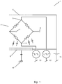
- Fig. 1 is a diagrammatic view of a sensor 1 according to a first embodiment of the invention.
- the sensor 1 comprises an n-dosed substrate 2.
- the substrate 2 illustrated in Fig. 1 is an n-dosed substrate, it is within the scope of the present invention that the substrate 2 could be a p-dosed substrate. In this case the anode cathode of the illustrated diodes should be reversed.
- a Wheatstone bridge 3 is arranged on the substrate 2, e.g. formed directly in the substrate 2 in a manner which will be described below with reference to Fig. 4 .
- a field shield 4 is arranged on the substrate 2 in such a manner that it covers the Wheatstone bridge 3. Thereby the field shield 4 shields the Wheatstone bridge 3 against external electrical fields.
- a power supply is arranged to supply a first voltage level, V 1 , in the form of a DC voltage to the substrate 2 and to the field shield 4. Furthermore, the power supply supplies a second voltage level, V 2 , in the form of a first quasi-DC voltage to a first node 5 of the Wheatstone bridge 3, and a third voltage level, V 3 , in the form of a second 'quasi-DC voltage to a second node 6 of the Wheatstone bridge 3. Accordingly, the voltages, V 2 and V 3 , both alternate between an upper level and a lower level in such a manner that the voltage is initially maintained substantially constant at the upper level, then switched abruptly to the lower level and maintained substantially constant at the lower level before being switched abruptly back to the upper level, etc.
- each of the quasi-DC voltages, V 2 and V 3 defines a period, e.g. being the time elapsing from the voltage is switched to the upper level until the voltage is once again switched to the upper level. Furthermore, when the upper voltage level is supplied to the first node 5, the lower voltage level is supplied to the second node 6, and vice versa.
- the quasi-DC voltages, V 2 and V 3 are selected in such a manner that, at any time during a period of the quasi-DC voltages, the DC voltage, V 1 , is higher than or equal to the quasi-DC voltages, V 2 and V 3 .
- the quasi-DC voltages, V 2 and V 3 may be equal to the DC voltage, V 1 , during the part of the period where the quasi-DC voltages are at the upper voltage level. However, for the remaining part of the period, i.e.
- the DC voltage, V 1 which is supplied to the substrate 2 and to the field shield 4, will be higher than the quasi-DC voltages, V 2 and V 3 .
- the DC voltage, V 1 may even be higher than the quasi-DC voltages, V 2 and V 3 , during the entire period of the 'quasi-DC voltages.
- the quasi-DC voltages, V 2 and V 3 are selected in such a manner that, at any time during a period of the quasi-DC voltages, the DC voltage, V 1 , is lower than or equal to the quasi-DC voltages, V 2 and V 3 .
- the DC voltage, V 1 is lower than the quasi-DC voltages, V 2 and V 3 , for at least a part of the period defined by the quasi-DC voltages.
- a voltage difference exists between the voltage level supplied to the substrate 2 and the field shield 4, on the one hand, and the first 5 and second 6 nodes of the Wheatstone bridge 3, on the other hand, at least for a part of the period defined by the quasi-DC voltages. This ensures that the capacitance between the four nodes of the Wheatstone bridge 3 and a casing or chassis 18 of the sensor 1 is minimised, and thereby that the electromagnetic interference effects are reduced.
- the sensor 1 of Fig. 1 may be operated in the following manner. Measuring electronics are connected to nodes 7 and 8 of the Wheatstone bridge 3. Voltages are supplied to the substrate 2, the field shield 4 and the first 5 and second 6 nodes of the Wheatstone bridge 3 as described above. Changes in a quantity to be measured, such as pressure, strain, stress, temperature, etc., cause the resistances of the resistors of the Wheatstone bridge 3 to change. This will, in turn, cause the voltage difference between nodes 7 and 8 to change. This change in voltage difference is detected by the measuring electronics, and is used for deriving the changes in the quantity being measured. With an appropriate calibration of the sensor 1, an absolute value of the quantity being measured can be derived.
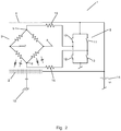
- Fig. 2 is a diagrammatic view of a sensor 1 according to a second embodiment of the invention.
- the sensor 1 of Fig. 2 is very similar to the sensor 1 of Fig. 1 , and it will therefore not be described in detail here.
- the sensor 1 of Fig. 2 comprises a switching arrangement 9 comprising four switches 10, 11, 12, 13 which can be alternatingly opened and closed. In Fig. 2 all four switches 10, 11, 12, 13 are shown in the open position.
- the switching arrangement 9 is electrically connected between a DC power supply 14 and the Wheatstone bridge 3.
- the DC power supply 14 is also electrically connected to the substrate 2 and the field shield 4 in such a manner that the DC voltage level supplied by the power supply 14 is the DC voltage level which is supplied to the substrate 2 and the field shield 4.
- a first biasing resistor 15 is arranged between the switching arrangement 9 and the first node 5 of the Wheatstone bridge 3, and a second biasing resistor 16 is arranged between the switching arrangement 9 and the second node 6 of the Wheatstone bridge 3.
- the biasing resistors 15, 16 lower the voltage level supplied by the DC power supply 14. Thereby, even the upper voltage level of the quasi-DC voltages supplied to the first 5 and second 6 nodes of the Wheatstone bridge 3, is lower than the DC voltage level supplied to the substrate 2 and the field shield 4.
- Fig. 3 illustrates the voltage levels, V 1 , V 2 and V 3 , supplied to the substrate 2, the field shield 4 and the Wheatstone bridge 3 of the sensor 1 of Fig. 1 , as a function of time.
- Fig. 3 illustrates the situation where the substrate 2 is an n-dosed substrate.
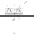
- Fig. 4 is a cross sectional view of a sensor 1 according to an embodiment of the invention.
- the sensor 1 comprises an n-dosed substrate 2, into which resistors 17 of a p-dosed material are formed.
- the resistors 17 form a Wheatstone bridge, and the sensor 1 may therefore, e.g., be of the kind shown in Fig. 1 or of the kind shown in Fig. 2 .
- a field shield 4 is arranged on the substrate 2 in such a manner that it covers the resistors 17.
- Voltages can be supplied to the substrate 2, the field shield 4 and the resistors 17 in the manner described above.
Landscapes
- Physics & Mathematics (AREA)
- General Physics & Mathematics (AREA)
- Pressure Sensors (AREA)
- Measuring Fluid Pressure (AREA)
Claims (14)
- Sensor (1), umfassend:- ein n-dotiertes Substrat (2),- Messelektronik, die zumindest teilweise auf dem Substrat (2) angeordnet ist, wobei die Messelektronik eine Wheatstone-Brücke (3) umfasst,
gekennzeichnet durch- eine Feldabschirmung (4), die derart auf dem Substrat (2) angeordnet ist, dass die Feldabschirmung (4) die Wheatstone-Brücke (3) abdeckt,- eine Stromversorgung, die so angeordnet ist, dass sie dem Substrat (2) und der Messelektronik eine elektrische Spannung zuführt, und zwar derart, dass:- der Wheatstone-Brücke (3) eine Quasi-Gleichspannung zugeführt wird, und- dem Substrat (2) eine Gleichspannung zugeführt wird, wobei der Pegel der Gleichspannung größer oder gleich der an die Wheatstone-Brücke (3) gelieferten Quasi-Gleichspannung ist. - Sensor (1) nach Anspruch 1, wobei die Stromversorgung ferner so angeordnet ist, dass sie der Feldabschirmung (4) eine elektrische Spannung zuführt, so dass der Pegel der der Feldabschirmung zugeführten Spannung größer oder gleich der der Wheatstone-Brücke (3) zugeführten Quasi-Gleichspannung ist.
- Sensor (1) nach Anspruch 2, wobei der Pegel der dem Substrat (2) zugeführten Gleichspannung gleich dem Pegel der der Feldabschirmung (4) zugeführten Spannung ist.
- Sensor (1) nach Anspruch 2, wobei die der Feldabschirmung (4) zugeführte Spannung der der Wheatstone-Brücke (3) zugeführten Quasi-Gleichspannung folgt.
- Sensor (1) nach einem der vorstehenden Ansprüche, wobei die Differenz zwischen dem dem Substrat (2) zugeführten Gleichspannungspegel und der der Wheatstone-Brücke (3) zugeführten Quasi-Gleichspannung mindestens 0,5 V beträgt.
- Sensor nach einem der vorstehenden Ansprüche, wobei die Messelektronik ferner einen oder mehrere Widerstände (15, 16) umfasst, wobei jeder Widerstand (15, 16) zwischen der Stromversorgung und einem Erregerknoten (5, 6) der Wheatstone-Brücke (3) elektrisch verbunden ist.
- Sensor (1) nach einem der vorstehenden Ansprüche, wobei die Wheatstone-Brücke (3) durch p-dotierte Widerstände (17) gebildet wird, die in dem Substrat (2) implementiert sind.
- Sensor (1) nach einem der vorstehenden Ansprüche, wobei der Sensor (1) ein piezoresistiver MEMS-Sensorchip ist.
- Sensor (1) nach einem der vorstehenden Ansprüche, wobei die Messelektronik ferner eine Schaltanordnung (9) umfasst, wobei die Schaltanordnung (9) so angeordnet ist, dass sie ein Quasi- Gleichspannungssignal erzeugt und das erzeugte Quasi- Gleichspannungssignal der Wheatstone Brücke (3) zuführt.
- Sensor (1) nach einem der vorstehenden Ansprüche, wobei der Sensor (1) ein Drucksensor ist.
- Sensor (1), umfassend:- ein p-dotiertes Substrat (2),- Messelektronik, die zumindest teilweise auf dem Substrat (2) angeordnet ist, wobei die Messelektronik eine Wheatstone-Brücke (3) umfasst,
gekennzeichnet durch- eine Feldabschirmung (4), die derart auf dem Substrat (2) angeordnet ist, dass die Feldabschirmung die Wheatstone-Brücke (3) abdeckt,- eine Stromversorgung, die so angeordnet ist, dass sie dem Substrat (2) und der Messelektronik eine elektrische Spannung zuführt, und zwar derart, dass:- der Wheatstone-Brücke (3) eine Quasi-Gleichspannung zugeführt wird, und- dem Substrat (2) eine Gleichspannung zugeführt wird, wobei der Pegel der Gleichspannung kleiner oder gleich der an die Wheatstone-Brücke (3) gelieferten Quasi-Gleichspannung ist. - Sensor (1) nach Anspruch 11, wobei die Stromversorgung ferner so angeordnet ist, dass sie der Feldabschirmung (4) eine elektrische Spannung zuführt, so dass der Pegel der der Feldabschirmung zugeführten Spannung kleiner oder gleich der der Wheatstone-Brücke (3) zugeführten Quasi-Gleichspannung ist.
- Sensor (1) nach einem der Ansprüche 11 oder 12, wobei die Wheatstone-Brücke (3) durch n-dotierte Widerstände (17) gebildet wird, die in dem Substrat (2) implementiert sind.
- Sensor (1) nach einem der Ansprüche 11-13, wobei der Sensor (1) ein Drucksensor ist.
Applications Claiming Priority (2)
| Application Number | Priority Date | Filing Date | Title |
|---|---|---|---|
| DKPA201200800 | 2012-12-17 | ||
| PCT/DK2013/050400 WO2014094777A1 (en) | 2012-12-17 | 2013-11-28 | A sensor comprising a substrate |
Publications (2)
| Publication Number | Publication Date |
|---|---|
| EP2932218A1 EP2932218A1 (de) | 2015-10-21 |
| EP2932218B1 true EP2932218B1 (de) | 2018-09-19 |
Family
ID=49683386
Family Applications (1)
| Application Number | Title | Priority Date | Filing Date |
|---|---|---|---|
| EP13798922.4A Active EP2932218B1 (de) | 2012-12-17 | 2013-11-28 | Sensor mit einem substrat. |
Country Status (5)
| Country | Link |
|---|---|
| US (1) | US20150309083A1 (de) |
| EP (1) | EP2932218B1 (de) |
| CN (1) | CN104870960B (de) |
| IN (1) | IN2015DN04191A (de) |
| WO (1) | WO2014094777A1 (de) |
Families Citing this family (7)
| Publication number | Priority date | Publication date | Assignee | Title |
|---|---|---|---|---|
| US9726705B2 (en) * | 2014-08-12 | 2017-08-08 | Hamilton Sundstrand Corporation | Sensor interface circuits |
| CN106354328B (zh) * | 2016-09-14 | 2023-11-14 | 宸鸿科技(厦门)有限公司 | 压力感测模组、压力感测触控系统 |
| DE102017126816B4 (de) * | 2017-11-15 | 2020-03-12 | Kriwan Industrie-Elektronik Gmbh | Verdichter |
| CN111051820B (zh) * | 2019-08-05 | 2022-03-15 | 深圳市汇顶科技股份有限公司 | 电桥传感器的检测电路、芯片及检测系统 |
| US11353373B2 (en) * | 2020-05-29 | 2022-06-07 | Stmicroelectronics Asia Pacific Pte Ltd | Strain gauge pattern to prevent variation due to temperature |
| DE102021211561A1 (de) * | 2020-11-19 | 2022-05-19 | Vitesco Technologies USA, LLC | Mems-druckerfassungselement mit spannungsjustierern |
| CN113030803A (zh) * | 2021-03-01 | 2021-06-25 | 歌尔微电子股份有限公司 | 磁传感器、磁传感器的制备方法及电子设备 |
Family Cites Families (13)
| Publication number | Priority date | Publication date | Assignee | Title |
|---|---|---|---|---|
| US4058254A (en) * | 1968-01-26 | 1977-11-15 | Danfoss A/S | Temperature-monitoring and control system |
| US4777826A (en) * | 1985-06-20 | 1988-10-18 | Rosemount Inc. | Twin film strain gauge system |
| JPH01147331A (ja) * | 1987-12-03 | 1989-06-09 | Ngk Insulators Ltd | 圧力検出器 |
| DE19917261C5 (de) * | 1999-04-16 | 2010-09-09 | Siemens Flow Instruments A/S | Elektromagnetische Durchflußmesseranordnung |
| US6422088B1 (en) * | 1999-09-24 | 2002-07-23 | Denso Corporation | Sensor failure or abnormality detecting system incorporated in a physical or dynamic quantity detecting apparatus |
| DE10160794B4 (de) * | 2001-12-11 | 2006-07-27 | Parker Hannifin Gmbh | Signalverarbeitungseinrichtung für einen Druckschalter od. dgl. |
| JP2005221453A (ja) * | 2004-02-09 | 2005-08-18 | Denso Corp | 圧力センサ |
| US7208691B2 (en) * | 2004-11-12 | 2007-04-24 | Eastman Kodak Company | Touch screen having undercut spacer dots |
| JP4421511B2 (ja) * | 2005-05-30 | 2010-02-24 | 三菱電機株式会社 | 半導体圧力センサ |
| JP4556784B2 (ja) * | 2005-06-27 | 2010-10-06 | 株式会社デンソー | 圧力センサ |
| DE102007011878A1 (de) * | 2007-03-13 | 2008-09-18 | Hydac Electronic Gmbh | Isolatorschichtsystem für einen Sensor und Sensor mit einem solchen Isolatorschichtsystem |
| WO2012080811A1 (ja) * | 2010-12-15 | 2012-06-21 | パナソニック株式会社 | 半導体圧力センサ |
| DE102011004577B4 (de) * | 2011-02-23 | 2023-07-27 | Robert Bosch Gmbh | Bauelementträger, Verfahren zur Herstellung eines solchen Bauelementträgers sowie Bauteil mit einem MEMS-Bauelement auf einem solchen Bauelementträger |
-
2013
- 2013-11-28 US US14/649,769 patent/US20150309083A1/en not_active Abandoned
- 2013-11-28 WO PCT/DK2013/050400 patent/WO2014094777A1/en not_active Ceased
- 2013-11-28 CN CN201380062165.5A patent/CN104870960B/zh active Active
- 2013-11-28 EP EP13798922.4A patent/EP2932218B1/de active Active
-
2015
- 2015-05-15 IN IN4191DEN2015 patent/IN2015DN04191A/en unknown
Non-Patent Citations (1)
| Title |
|---|
| None * |
Also Published As
| Publication number | Publication date |
|---|---|
| EP2932218A1 (de) | 2015-10-21 |
| CN104870960A (zh) | 2015-08-26 |
| WO2014094777A1 (en) | 2014-06-26 |
| CN104870960B (zh) | 2017-05-17 |
| IN2015DN04191A (de) | 2015-10-16 |
| US20150309083A1 (en) | 2015-10-29 |
Similar Documents
| Publication | Publication Date | Title |
|---|---|---|
| US20150309083A1 (en) | A sensor comprising a substrate | |
| US10777393B2 (en) | Process condition sensing device and method for plasma chamber | |
| US7605580B2 (en) | Integrated hybrid current sensor | |
| TWI648527B (zh) | 改良的壓力感測器結構 | |
| EP3066487B1 (de) | Auslesesystem für hallsensor mit offset-bestimmung unter verwendung des hallelements selbst | |
| EP2458359B1 (de) | Halbleiterdrucksensor, drucksensorvorrichtung, elektronische vorrichtung und verfahren zur herstellung des halbleiterdrucksensors | |
| CN104755895B (zh) | 具有覆盖层的压力传感器 | |
| US7219554B2 (en) | Semiconductor pressure sensor | |
| CN105910735B (zh) | 机械应力的探测与补偿 | |
| US9557237B2 (en) | MEMS pressure sensor field shield layout for surface charge immunity in oil filled packaging | |
| US9909944B2 (en) | Thin film sensor | |
| EP2878940B1 (de) | MEMS-Drucksensor-Feldabschirmungslayout für Oberflächenladungsimmunität in ölgefülltem Gehäuse | |
| US20160245706A1 (en) | Multi-sensor assembly | |
| CN113985100A (zh) | 具有集成电屏蔽的改进型电流感测装置 | |
| CN103081110B (zh) | 多传感器集成电路设备 | |
| JP2014048237A (ja) | 磁気ホールセンサー | |
| JP2010117179A (ja) | 力検知素子 | |
| JP5866496B2 (ja) | 半導体圧力センサ | |
| KR102165935B1 (ko) | 전류센서 및 그의 제조방법 | |
| JP2009257916A (ja) | 静電容量型圧力センサ及び静電容量の補償信号の提供方法 | |
| KR20200126347A (ko) | 전류센서 및 그의 제조방법 | |
| WO2012007634A1 (en) | Radiation detector, pitch adapter, and method for producing a pitch adapter | |
| JP2015200549A (ja) | 圧力センサ |
Legal Events
| Date | Code | Title | Description |
|---|---|---|---|
| PUAI | Public reference made under article 153(3) epc to a published international application that has entered the european phase |
Free format text: ORIGINAL CODE: 0009012 |
|
| 17P | Request for examination filed |
Effective date: 20150519 |
|
| AK | Designated contracting states |
Kind code of ref document: A1 Designated state(s): AL AT BE BG CH CY CZ DE DK EE ES FI FR GB GR HR HU IE IS IT LI LT LU LV MC MK MT NL NO PL PT RO RS SE SI SK SM TR |
|
| AX | Request for extension of the european patent |
Extension state: BA ME |
|
| DAX | Request for extension of the european patent (deleted) | ||
| GRAP | Despatch of communication of intention to grant a patent |
Free format text: ORIGINAL CODE: EPIDOSNIGR1 |
|
| STAA | Information on the status of an ep patent application or granted ep patent |
Free format text: STATUS: GRANT OF PATENT IS INTENDED |
|
| INTG | Intention to grant announced |
Effective date: 20180509 |
|
| GRAS | Grant fee paid |
Free format text: ORIGINAL CODE: EPIDOSNIGR3 |
|
| GRAJ | Information related to disapproval of communication of intention to grant by the applicant or resumption of examination proceedings by the epo deleted |
Free format text: ORIGINAL CODE: EPIDOSDIGR1 |
|
| GRAL | Information related to payment of fee for publishing/printing deleted |
Free format text: ORIGINAL CODE: EPIDOSDIGR3 |
|
| STAA | Information on the status of an ep patent application or granted ep patent |
Free format text: STATUS: REQUEST FOR EXAMINATION WAS MADE |
|
| GRAR | Information related to intention to grant a patent recorded |
Free format text: ORIGINAL CODE: EPIDOSNIGR71 |
|
| STAA | Information on the status of an ep patent application or granted ep patent |
Free format text: STATUS: GRANT OF PATENT IS INTENDED |
|
| GRAA | (expected) grant |
Free format text: ORIGINAL CODE: 0009210 |
|
| STAA | Information on the status of an ep patent application or granted ep patent |
Free format text: STATUS: THE PATENT HAS BEEN GRANTED |
|
| INTC | Intention to grant announced (deleted) | ||
| AK | Designated contracting states |
Kind code of ref document: B1 Designated state(s): AL AT BE BG CH CY CZ DE DK EE ES FI FR GB GR HR HU IE IS IT LI LT LU LV MC MK MT NL NO PL PT RO RS SE SI SK SM TR |
|
| INTG | Intention to grant announced |
Effective date: 20180810 |
|
| REG | Reference to a national code |
Ref country code: GB Ref legal event code: FG4D |
|
| REG | Reference to a national code |
Ref country code: CH Ref legal event code: EP |
|
| REG | Reference to a national code |
Ref country code: AT Ref legal event code: REF Ref document number: 1043805 Country of ref document: AT Kind code of ref document: T Effective date: 20181015 |
|
| REG | Reference to a national code |
Ref country code: IE Ref legal event code: FG4D |
|
| REG | Reference to a national code |
Ref country code: DE Ref legal event code: R096 Ref document number: 602013043953 Country of ref document: DE |
|
| REG | Reference to a national code |
Ref country code: NL Ref legal event code: MP Effective date: 20180919 |
|
| PG25 | Lapsed in a contracting state [announced via postgrant information from national office to epo] |
Ref country code: GR Free format text: LAPSE BECAUSE OF FAILURE TO SUBMIT A TRANSLATION OF THE DESCRIPTION OR TO PAY THE FEE WITHIN THE PRESCRIBED TIME-LIMIT Effective date: 20181220 Ref country code: FI Free format text: LAPSE BECAUSE OF FAILURE TO SUBMIT A TRANSLATION OF THE DESCRIPTION OR TO PAY THE FEE WITHIN THE PRESCRIBED TIME-LIMIT Effective date: 20180919 Ref country code: LT Free format text: LAPSE BECAUSE OF FAILURE TO SUBMIT A TRANSLATION OF THE DESCRIPTION OR TO PAY THE FEE WITHIN THE PRESCRIBED TIME-LIMIT Effective date: 20180919 Ref country code: BG Free format text: LAPSE BECAUSE OF FAILURE TO SUBMIT A TRANSLATION OF THE DESCRIPTION OR TO PAY THE FEE WITHIN THE PRESCRIBED TIME-LIMIT Effective date: 20181219 Ref country code: SE Free format text: LAPSE BECAUSE OF FAILURE TO SUBMIT A TRANSLATION OF THE DESCRIPTION OR TO PAY THE FEE WITHIN THE PRESCRIBED TIME-LIMIT Effective date: 20180919 Ref country code: RS Free format text: LAPSE BECAUSE OF FAILURE TO SUBMIT A TRANSLATION OF THE DESCRIPTION OR TO PAY THE FEE WITHIN THE PRESCRIBED TIME-LIMIT Effective date: 20180919 Ref country code: NO Free format text: LAPSE BECAUSE OF FAILURE TO SUBMIT A TRANSLATION OF THE DESCRIPTION OR TO PAY THE FEE WITHIN THE PRESCRIBED TIME-LIMIT Effective date: 20181219 |
|
| REG | Reference to a national code |
Ref country code: LT Ref legal event code: MG4D |
|
| PG25 | Lapsed in a contracting state [announced via postgrant information from national office to epo] |
Ref country code: HR Free format text: LAPSE BECAUSE OF FAILURE TO SUBMIT A TRANSLATION OF THE DESCRIPTION OR TO PAY THE FEE WITHIN THE PRESCRIBED TIME-LIMIT Effective date: 20180919 Ref country code: AL Free format text: LAPSE BECAUSE OF FAILURE TO SUBMIT A TRANSLATION OF THE DESCRIPTION OR TO PAY THE FEE WITHIN THE PRESCRIBED TIME-LIMIT Effective date: 20180919 Ref country code: LV Free format text: LAPSE BECAUSE OF FAILURE TO SUBMIT A TRANSLATION OF THE DESCRIPTION OR TO PAY THE FEE WITHIN THE PRESCRIBED TIME-LIMIT Effective date: 20180919 |
|
| REG | Reference to a national code |
Ref country code: AT Ref legal event code: MK05 Ref document number: 1043805 Country of ref document: AT Kind code of ref document: T Effective date: 20180919 |
|
| PG25 | Lapsed in a contracting state [announced via postgrant information from national office to epo] |
Ref country code: CZ Free format text: LAPSE BECAUSE OF FAILURE TO SUBMIT A TRANSLATION OF THE DESCRIPTION OR TO PAY THE FEE WITHIN THE PRESCRIBED TIME-LIMIT Effective date: 20180919 Ref country code: RO Free format text: LAPSE BECAUSE OF FAILURE TO SUBMIT A TRANSLATION OF THE DESCRIPTION OR TO PAY THE FEE WITHIN THE PRESCRIBED TIME-LIMIT Effective date: 20180919 Ref country code: AT Free format text: LAPSE BECAUSE OF FAILURE TO SUBMIT A TRANSLATION OF THE DESCRIPTION OR TO PAY THE FEE WITHIN THE PRESCRIBED TIME-LIMIT Effective date: 20180919 Ref country code: IT Free format text: LAPSE BECAUSE OF FAILURE TO SUBMIT A TRANSLATION OF THE DESCRIPTION OR TO PAY THE FEE WITHIN THE PRESCRIBED TIME-LIMIT Effective date: 20180919 Ref country code: EE Free format text: LAPSE BECAUSE OF FAILURE TO SUBMIT A TRANSLATION OF THE DESCRIPTION OR TO PAY THE FEE WITHIN THE PRESCRIBED TIME-LIMIT Effective date: 20180919 Ref country code: NL Free format text: LAPSE BECAUSE OF FAILURE TO SUBMIT A TRANSLATION OF THE DESCRIPTION OR TO PAY THE FEE WITHIN THE PRESCRIBED TIME-LIMIT Effective date: 20180919 Ref country code: IS Free format text: LAPSE BECAUSE OF FAILURE TO SUBMIT A TRANSLATION OF THE DESCRIPTION OR TO PAY THE FEE WITHIN THE PRESCRIBED TIME-LIMIT Effective date: 20190119 Ref country code: ES Free format text: LAPSE BECAUSE OF FAILURE TO SUBMIT A TRANSLATION OF THE DESCRIPTION OR TO PAY THE FEE WITHIN THE PRESCRIBED TIME-LIMIT Effective date: 20180919 Ref country code: PL Free format text: LAPSE BECAUSE OF FAILURE TO SUBMIT A TRANSLATION OF THE DESCRIPTION OR TO PAY THE FEE WITHIN THE PRESCRIBED TIME-LIMIT Effective date: 20180919 |
|
| PG25 | Lapsed in a contracting state [announced via postgrant information from national office to epo] |
Ref country code: PT Free format text: LAPSE BECAUSE OF FAILURE TO SUBMIT A TRANSLATION OF THE DESCRIPTION OR TO PAY THE FEE WITHIN THE PRESCRIBED TIME-LIMIT Effective date: 20190119 Ref country code: SK Free format text: LAPSE BECAUSE OF FAILURE TO SUBMIT A TRANSLATION OF THE DESCRIPTION OR TO PAY THE FEE WITHIN THE PRESCRIBED TIME-LIMIT Effective date: 20180919 Ref country code: SM Free format text: LAPSE BECAUSE OF FAILURE TO SUBMIT A TRANSLATION OF THE DESCRIPTION OR TO PAY THE FEE WITHIN THE PRESCRIBED TIME-LIMIT Effective date: 20180919 |
|
| REG | Reference to a national code |
Ref country code: DE Ref legal event code: R097 Ref document number: 602013043953 Country of ref document: DE |
|
| REG | Reference to a national code |
Ref country code: CH Ref legal event code: PL |
|
| PLBE | No opposition filed within time limit |
Free format text: ORIGINAL CODE: 0009261 |
|
| STAA | Information on the status of an ep patent application or granted ep patent |
Free format text: STATUS: NO OPPOSITION FILED WITHIN TIME LIMIT |
|
| PG25 | Lapsed in a contracting state [announced via postgrant information from national office to epo] |
Ref country code: MC Free format text: LAPSE BECAUSE OF FAILURE TO SUBMIT A TRANSLATION OF THE DESCRIPTION OR TO PAY THE FEE WITHIN THE PRESCRIBED TIME-LIMIT Effective date: 20180919 Ref country code: LU Free format text: LAPSE BECAUSE OF NON-PAYMENT OF DUE FEES Effective date: 20181128 Ref country code: DK Free format text: LAPSE BECAUSE OF FAILURE TO SUBMIT A TRANSLATION OF THE DESCRIPTION OR TO PAY THE FEE WITHIN THE PRESCRIBED TIME-LIMIT Effective date: 20180919 |
|
| REG | Reference to a national code |
Ref country code: BE Ref legal event code: MM Effective date: 20181130 |
|
| REG | Reference to a national code |
Ref country code: IE Ref legal event code: MM4A |
|
| 26N | No opposition filed |
Effective date: 20190620 |
|
| PG25 | Lapsed in a contracting state [announced via postgrant information from national office to epo] |
Ref country code: CH Free format text: LAPSE BECAUSE OF NON-PAYMENT OF DUE FEES Effective date: 20181130 Ref country code: LI Free format text: LAPSE BECAUSE OF NON-PAYMENT OF DUE FEES Effective date: 20181130 |
|
| PG25 | Lapsed in a contracting state [announced via postgrant information from national office to epo] |
Ref country code: IE Free format text: LAPSE BECAUSE OF NON-PAYMENT OF DUE FEES Effective date: 20181128 Ref country code: SI Free format text: LAPSE BECAUSE OF FAILURE TO SUBMIT A TRANSLATION OF THE DESCRIPTION OR TO PAY THE FEE WITHIN THE PRESCRIBED TIME-LIMIT Effective date: 20180919 |
|
| PG25 | Lapsed in a contracting state [announced via postgrant information from national office to epo] |
Ref country code: BE Free format text: LAPSE BECAUSE OF NON-PAYMENT OF DUE FEES Effective date: 20181130 |
|
| PG25 | Lapsed in a contracting state [announced via postgrant information from national office to epo] |
Ref country code: MT Free format text: LAPSE BECAUSE OF NON-PAYMENT OF DUE FEES Effective date: 20181128 |
|
| PG25 | Lapsed in a contracting state [announced via postgrant information from national office to epo] |
Ref country code: TR Free format text: LAPSE BECAUSE OF FAILURE TO SUBMIT A TRANSLATION OF THE DESCRIPTION OR TO PAY THE FEE WITHIN THE PRESCRIBED TIME-LIMIT Effective date: 20180919 |
|
| PG25 | Lapsed in a contracting state [announced via postgrant information from national office to epo] |
Ref country code: HU Free format text: LAPSE BECAUSE OF FAILURE TO SUBMIT A TRANSLATION OF THE DESCRIPTION OR TO PAY THE FEE WITHIN THE PRESCRIBED TIME-LIMIT; INVALID AB INITIO Effective date: 20131128 Ref country code: MK Free format text: LAPSE BECAUSE OF NON-PAYMENT OF DUE FEES Effective date: 20180919 Ref country code: CY Free format text: LAPSE BECAUSE OF FAILURE TO SUBMIT A TRANSLATION OF THE DESCRIPTION OR TO PAY THE FEE WITHIN THE PRESCRIBED TIME-LIMIT Effective date: 20180919 |
|
| P01 | Opt-out of the competence of the unified patent court (upc) registered |
Effective date: 20230617 |
|
| PGFP | Annual fee paid to national office [announced via postgrant information from national office to epo] |
Ref country code: DE Payment date: 20251007 Year of fee payment: 13 |
|
| PGFP | Annual fee paid to national office [announced via postgrant information from national office to epo] |
Ref country code: GB Payment date: 20251016 Year of fee payment: 13 |
|
| PGFP | Annual fee paid to national office [announced via postgrant information from national office to epo] |
Ref country code: FR Payment date: 20251023 Year of fee payment: 13 |