EP2930743B1 - Halbleiterisolationsstruktur - Google Patents
Halbleiterisolationsstruktur Download PDFInfo
- Publication number
- EP2930743B1 EP2930743B1 EP14164475.7A EP14164475A EP2930743B1 EP 2930743 B1 EP2930743 B1 EP 2930743B1 EP 14164475 A EP14164475 A EP 14164475A EP 2930743 B1 EP2930743 B1 EP 2930743B1
- Authority
- EP
- European Patent Office
- Prior art keywords
- region
- voltage
- semiconductor
- insulating
- semiconductor region
- Prior art date
- Legal status (The legal status is an assumption and is not a legal conclusion. Google has not performed a legal analysis and makes no representation as to the accuracy of the status listed.)
- Active
Links
Images


Classifications
-
- H—ELECTRICITY
- H10—SEMICONDUCTOR DEVICES; ELECTRIC SOLID-STATE DEVICES NOT OTHERWISE PROVIDED FOR
- H10D—INORGANIC ELECTRIC SEMICONDUCTOR DEVICES
- H10D89/00—Aspects of integrated devices not covered by groups H10D84/00 - H10D88/00
- H10D89/60—Integrated devices comprising arrangements for electrical or thermal protection, e.g. protection circuits against electrostatic discharge [ESD]
-
- H—ELECTRICITY
- H10—SEMICONDUCTOR DEVICES; ELECTRIC SOLID-STATE DEVICES NOT OTHERWISE PROVIDED FOR
- H10D—INORGANIC ELECTRIC SEMICONDUCTOR DEVICES
- H10D8/00—Diodes
- H10D8/20—Breakdown diodes, e.g. avalanche diodes
- H10D8/25—Zener diodes
-
- H10W10/014—
-
- H10W10/17—
-
- H—ELECTRICITY
- H02—GENERATION; CONVERSION OR DISTRIBUTION OF ELECTRIC POWER
- H02H—EMERGENCY PROTECTIVE CIRCUIT ARRANGEMENTS
- H02H9/00—Emergency protective circuit arrangements for limiting excess current or voltage without disconnection
- H02H9/04—Emergency protective circuit arrangements for limiting excess current or voltage without disconnection responsive to excess voltage
- H02H9/045—Emergency protective circuit arrangements for limiting excess current or voltage without disconnection responsive to excess voltage adapted to a particular application and not provided for elsewhere
- H02H9/046—Emergency protective circuit arrangements for limiting excess current or voltage without disconnection responsive to excess voltage adapted to a particular application and not provided for elsewhere responsive to excess voltage appearing at terminals of integrated circuits
-
- H—ELECTRICITY
- H05—ELECTRIC TECHNIQUES NOT OTHERWISE PROVIDED FOR
- H05K—PRINTED CIRCUITS; CASINGS OR CONSTRUCTIONAL DETAILS OF ELECTRIC APPARATUS; MANUFACTURE OF ASSEMBLAGES OF ELECTRICAL COMPONENTS
- H05K1/00—Printed circuits
- H05K1/02—Details
- H05K1/0213—Electrical arrangements not otherwise provided for
- H05K1/0254—High voltage adaptations; Electrical insulation details; Overvoltage or electrostatic discharge protection ; Arrangements for regulating voltages or for using plural voltages
- H05K1/0257—Overvoltage protection
- H05K1/0259—Electrostatic discharge [ESD] protection
-
- H—ELECTRICITY
- H10—SEMICONDUCTOR DEVICES; ELECTRIC SOLID-STATE DEVICES NOT OTHERWISE PROVIDED FOR
- H10D—INORGANIC ELECTRIC SEMICONDUCTOR DEVICES
- H10D8/00—Diodes
- H10D8/80—PNPN diodes, e.g. Shockley diodes or break-over diodes
-
- H—ELECTRICITY
- H10—SEMICONDUCTOR DEVICES; ELECTRIC SOLID-STATE DEVICES NOT OTHERWISE PROVIDED FOR
- H10D—INORGANIC ELECTRIC SEMICONDUCTOR DEVICES
- H10D84/00—Integrated devices formed in or on semiconductor substrates that comprise only semiconducting layers, e.g. on Si wafers or on GaAs-on-Si wafers
- H10D84/01—Manufacture or treatment
- H10D84/0123—Integrating together multiple components covered by H10D12/00 or H10D30/00, e.g. integrating multiple IGBTs
- H10D84/0126—Integrating together multiple components covered by H10D12/00 or H10D30/00, e.g. integrating multiple IGBTs the components including insulated gates, e.g. IGFETs
- H10D84/0165—Integrating together multiple components covered by H10D12/00 or H10D30/00, e.g. integrating multiple IGBTs the components including insulated gates, e.g. IGFETs the components including complementary IGFETs, e.g. CMOS devices
- H10D84/0188—Manufacturing their isolation regions
-
- H—ELECTRICITY
- H10—SEMICONDUCTOR DEVICES; ELECTRIC SOLID-STATE DEVICES NOT OTHERWISE PROVIDED FOR
- H10D—INORGANIC ELECTRIC SEMICONDUCTOR DEVICES
- H10D84/00—Integrated devices formed in or on semiconductor substrates that comprise only semiconducting layers, e.g. on Si wafers or on GaAs-on-Si wafers
- H10D84/01—Manufacture or treatment
- H10D84/02—Manufacture or treatment characterised by using material-based technologies
- H10D84/03—Manufacture or treatment characterised by using material-based technologies using Group IV technology, e.g. silicon technology or silicon-carbide [SiC] technology
- H10D84/038—Manufacture or treatment characterised by using material-based technologies using Group IV technology, e.g. silicon technology or silicon-carbide [SiC] technology using silicon technology, e.g. SiGe
-
- H—ELECTRICITY
- H10—SEMICONDUCTOR DEVICES; ELECTRIC SOLID-STATE DEVICES NOT OTHERWISE PROVIDED FOR
- H10D—INORGANIC ELECTRIC SEMICONDUCTOR DEVICES
- H10D89/00—Aspects of integrated devices not covered by groups H10D84/00 - H10D88/00
- H10D89/60—Integrated devices comprising arrangements for electrical or thermal protection, e.g. protection circuits against electrostatic discharge [ESD]
- H10D89/601—Integrated devices comprising arrangements for electrical or thermal protection, e.g. protection circuits against electrostatic discharge [ESD] for devices having insulated gate electrodes, e.g. for IGFETs or IGBTs
- H10D89/611—Integrated devices comprising arrangements for electrical or thermal protection, e.g. protection circuits against electrostatic discharge [ESD] for devices having insulated gate electrodes, e.g. for IGFETs or IGBTs using diodes as protective elements
Definitions
- the invention relates to a semiconductor isolation structure. More particularly, the present invention relates to a semiconductor isolation structure suitable for providing high voltage isolation.
- junction isolation in which a reverse biased p-n junction is used to create an electrically isolated region, or well, around a component.
- An alternative approach is to use an insulating material, such as a silicon oxide, to isolate various regions of semiconductor from each other.
- One technique for forming insulating structures to isolate regions of semiconducting material from each other is to define a trench in a semiconductor material, and then to form an insulating material in the trench. For example, a deep reactive ion etch may be used to form the trench, and a thermal oxidation process used to form the insulating material. The trench may subsequently be re-filled and planarised (e.g. by chemical mechanical polishing), so that further layers can be deposited over it.
- Such trench isolation structures are typically capable of standing off a limited voltage.
- the maximum standoff voltage is typically determined by the breakdown voltage of the structure, which will be affected by the thickness of the insulator in the trench and the geometry of the trench.
- One way of providing high voltage isolation in a semiconductor material is to separate devices with a drift region of the semiconductor material.
- the size of the drift region tends to be relatively large. For example, a drift region of over 100 ⁇ m may be necessary for 700V isolation.
- a 100 ⁇ m wide drift region around the perimeter of a high voltage region consumes a relatively large amount of die area, which is costly.
- a high voltage isolation structure with a smaller footprint would be preferable.
- US2010/0314710 discloses the use of three concentric, nested isolation trenches to provide isolation for high voltages.
- a semiconductor structure comprising: a first semiconductor region, a second semiconductor region within the first semiconductor region, and a voltage isolator separating the first and second semiconductor region, the voltage isolator comprising: a nested series of insulating regions around the perimeter of the second semiconductor region, an intermediate semiconductor region between each adjacent pair of nested insulating regions, and a voltage control device comprising a conducting element connected to at least one intermediate semiconductor region, in parallel with at least one insulating region, so as to control a voltage across the at least one insulating region.
- the voltage control device may help to define the voltage across each insulating region, for instance by preventing at least one intermediate region from having a floating voltage, or by limiting a voltage across at least one intermediate region to a breakdown voltage of the conducting element.
- each adjacent semiconductor region is unlikely to be equal (for example because they are nested, and therefore have different surface area), and hence the voltage drop over each insulating region will tend to be unequal.
- Connecting a conducting element in parallel with at least one intermediate semiconductor region allows the voltage across the at least one insulating region to be controlled, thereby improving the reliability of the isolation structure.
- the isolation structure may be suitable for isolating high voltages, for example, in excess of 100V, 200V, 300V, 400V, 500V, 750V or 1000V.
- the voltage of the first region may be higher than the voltage of the second region, or the voltage of the second region may be higher than the voltage of the first region.
- the voltage control device may be arranged to control the voltage in either of these cases (or both).
- Embodiments of the invention provide for a scalable voltage isolation in which additional insulating regions may simply be added to increase the voltage isolation to an arbitrary amount.
- the voltage control device may comprise a conducting element connected in parallel with each insulating region, so as to control the voltage across each insulating region.
- the voltage control device may comprise a plurality of conducting elements connected in series, each conducting element being connected in parallel with a corresponding insulating region, the voltage control device being connected at a first location to the first region, at a second location to the second region, and having intermediate connections between the first and second location to each intermediate semiconductor region. Such an arrangement allows the voltage across each insulating region to be controlled.
- each conducting element is a Zener diode (or a series combination of Zener diodes)
- the voltage across each insulating region will be limited to the breakdown voltage of the Zener diode.
- each conducting element may be a resistor
- the voltage control device may be a potential divider that defines the voltage of each intermediate semiconductor region. Providing a controlled current leakage path in parallel with each insulating region means that the voltage across each insulating region is defined
- the voltage control device may be at least partly defined in at least one of: the first semiconductor region, an intermediate semiconductor region and the second semiconductor region.
- a conducting element e.g. a Zener diode
- a further conducting element formed in either (or both of) the first or second region, thereby providing a conducting element corresponding with each insulating region.
- the first and second semiconductor region may be defined in the same semiconductor layer.
- the semiconductor layer may comprise: a bulk semiconductor material (e.g. silicon), a silicon on insulator layer or a semiconductor on insulator layer.
- Each non-conducting region may comprise a trench isolation structure.
- the trench isolation structure may be through a full thickness of the semiconductor layer. Such an arrangement may be particularly suitable for high voltage applications.
- Each conducting element may comprise a resistor.
- Each conducting element may have a relatively high resistance, so as to limit any current leakage when a voltage bias exists between the first and second region.
- Each conducting element may comprise a diode, or a plurality of diodes connected in series.
- the threshold voltage of a single diode may be below the limit voltage of the dielectric region.
- the voltage divider may comprise a plurality of diodes.
- a diode under reverse bias exhibits a breakdown voltage at which the current suddenly increases due to at least one of the Zener effect or avalanche breakdown effect.
- Diodes may therefore be used to limit the voltage step between the first end of the voltage divider and the intermediate connection, and between the intermediate connection and the second end of the voltage divider. Connecting diodes in series increases the effective breakdown voltage for the series of diodes, taken together.
- the (or each) diode may comprise a Zener diode. Zener diodes are configured to have a controlled breakdown voltage, and to allow current through the device to keep the voltage across the diode at the Zener (or breakdown) voltage.
- a semiconductor device comprising the semiconductor structure according to the first aspect of the invention, wherein the semiconductor structure is configured as: a high voltage Zener diode, or a high voltage clamp.
- the semiconductor structure is configured as: a high voltage Zener diode, or a high voltage clamp.
- Embodiments of the first aspect are particularly suitable for providing a high voltage Zener diode or high voltage clamp.
- an electronic apparatus comprising the semiconductor device according to the second aspect.
- the apparatus may comprise an integrated circuit for discharging a mains filtering capacitor, and the semiconductor device according to the second aspect may be configured to protect the integrated circuit from overvoltage damage due to mains surge.
- the semiconductor device may be integrated on a single die with the integrated circuit for discharging the mains filtering capacitor, thereby providing a lower cost solution than protecting such a device using an external component, such as a metal oxide varistor.
- Any integrated circuit that needs to be protected from high voltages may include a semiconductor device according to the second aspect, for instance configured as a voltage clamp.
- a method of fabricating the device according to the first or second aspect of the invention comprising: providing a semiconductor layer; defining a first and second semiconductor region of the semiconductor layer by forming a voltage isolator around a perimeter of the second semiconductor region, separating it from the first semiconductor region, the voltage isolator comprising a nested series of isolating regions, with an intermediate region of the semiconductor layer between each adjacent pair insulating regions; defining a voltage control device comprising a conducting element connected to at least one intermediate semiconductor region, in parallel with at least one insulating region, so as to control a voltage across the at least one insulating region.
- the method may provide for a low cost, scalable high voltage isolation structure that can be included with minimal process modification to facilitate high voltage functionality in an integrated circuit.
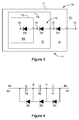
- a semiconductor structure 10 comprising a first semiconductor region R1, a second semiconductor region R2, and a voltage isolator 11 separating the first and second semiconductor region R1, R2.
- the second semiconductor region R2 is within the first semiconductor region R1, and the voltage isolator 11 surrounds the second region R2.
- the voltage isolator 11 comprises a nested series of insulating regions T1, T2 around the perimeter of the second semiconductor region R2. Between the two insulating regions T1, T2 is an intermediate semiconductor region I1.
- the voltage isolator 11 further comprises a voltage control device 12 comprising a conducting element, which in this embodiment is a diode D1.
- the diode D1 is connected at a first end 14 to the second semiconductor region R2, and at a second end 13 to the intermediate semiconductor region I1.
- the diode D1 may be a Zener diode, which will break down when a sufficiently large reverse bias voltage is present between the anode and the cathode thereof.
- the voltage between the second semiconductor region R2 and the intermediate semiconductor region I1 is thereby limited to the breakdown voltage of the diode D1. This can be used to prevent an unequal division of voltage across the two insulating regions T1 and T2.
- D1 is illustrated as a single diode, D1 may comprise more than one diode (such diodes are referred to herein as 'sub-diodes') connected in series, thereby providing an increased threshold voltage.
- the diode D1 may consist of a series of eight Zener sub-diodes, each with a threshold voltage of approximately 9.5V.
- the threshold voltage of the diode D1 would then be 76V.
- the diode D1 in Figure 1 is arranged to be reverse biased when the voltage in the first region R1 is greater than the voltage in the second region R2, but this could be reversed so that the diode D1 is reverse biased when the voltage of the second region R2 is higher than the voltage of the first region R1.
- the first and second semiconductor region R1, R2 and the intermediate semiconductor region I1 may be formed from a single semiconductor layer.
- the regions R1, R2 and I1 may comprise silicon, or another type of semiconductor material, such as a III-V semiconductor e.g. GaAs).
- the insulating regions T1, T2 may be trench isolation structures, formed by patterning a trench in the semiconductor layer, and at least partially filling or coating the interior with an insulator.
- Each trench T1, T2 may be formed by deep reactive ion etching, and the insulating material may comprise a thermal oxide (e.g. silicon oxide).
- the p-n junction of the diode D1 may be formed in the second semiconductor region R2 or the first intermediate semiconductor region R1, using conventional semiconductor processing techniques.
- FIG. 2 an equivalent circuit of Figure 1 is shown.
- the insulating regions T2, T1 are represented by capacitors between R2 and I1 and between I1 and R1 respectively. If the voltage control device 12 (comprising diode D1) were not present and R1 was at a higher voltage than R2, the voltage of the intermediate region I1 would float at a voltage determined by the relative capacitance of T1 and T2. If both capacitors T1 and T2 were equal, the voltage at I1 would be equal to half the voltage difference between R1 and R2. However, because the insulating regions T1 and T2 are nested T1 may have a larger capacitance resulting in an unequal distribution of voltage, with a higher voltage dropped across T2 than T1.
- the voltage control diode D1 is arranged to control the voltage across T2, and may be configured with a threshold voltage just below the maximum stand-off voltage of the insulating region T2.
- the diode D1 will thereby prevent the voltage across T2 from exceeding the maximum stand-off voltage of the insulating region T2, because it will conduct current when the voltage across D1 reaches the threshold voltage. Injection of charge into the intermediate semiconductor region I1 will increase the voltage at I1, and therefore increase the voltage drop across T1.
- the excess voltage across T2 (above the threshold of the diode D1) is therefore re-distributed by the diode D1 across T1.
- the voltage isolator 11 comprises a series of three nested insulating regions T1, T2 and T3.
- a first intermediate semiconductor region I1 is defined between T1 and T2 and a second intermediate semiconductor region I2 is defined between T2 and T3.
- the voltage control device 12 comprises three diodes D1, D2, D3.
- Each diode D1, D2, D3 is respectively connected across, i.e. in parallel with, a corresponding insulating region T1, T2, T3.
- the diodes D1-D3 are also connected to each other in series.
- the voltage control device 12 is connected at a first end 15 to the first region R1, at a second end 14 to the second region R2, and has intermediate connections 13 to each intermediate semiconductor region I1, I2.
- the diodes D1-D3 are arranged to be reverse biased when the voltage of the second region R2 is greater than the voltage of the first region R1, but the direction of the diodes can be reversed in other embodiments.
- the voltage across each of the insulating regions is controlled by the diode connected in parallel thereto.
- the maximum voltage across each insulating region T1-T3 is thereby limited by the threshold voltage of each diode D1-D3.
- This arrangement is scalable, and an arbitrary number of insulating regions and parallel connected diodes can be used to provide reliable voltage isolation for an arbitrary voltage.
- Figures 5 and 6 show an alternative embodiment of a semiconductor structure 10, in which the conducting elements of the voltage control device 12 comprise resistors r1-r3.
- the conducting elements of the voltage control device 12 comprise resistors r1-r3.
- the resistors r1-r3 of the voltage control device 12 are connected in series, and the voltage control device 12 is again connected at a first end 15 to the first region R1, at a second end 14 to the second region R2, and has intermediate connections 13 to each intermediate semiconductor region I1, I2.
- the resistors r1-r3 of the voltage control device thereby provide a voltage divider, which distributes the voltage of the otherwise floating intermediate regions I1 and I2 to a voltage that is defined by the ratio of the resistors.
- the resistors r1-r3 may all have substantially equal resistance, thereby fixing the voltage across each insulating region T1-T3 to be substantially the same.
- Each resistor r1-r3 may have a relatively large resistance, for example greater than 1 kohm or 1 Mohm, thereby limiting the leakage current through the voltage control device 12. Since resistors are not directional, this approach may be suitable for cases in which either the first or second region R1, R2 is at a high voltage.
- Figure 7 shows a schematic layout of a semiconductor structure 100 comprising a first semiconductor region R1 and a second semiconductor region R2 separated by a voltage isolator 11.
- the layout of Figure 7 shows layers corresponding only to a first metal layer 29, a second metal layer 30, a third metal layer 33 and a trench isolation 19. More complete views of the layers of the semiconductor structure can be seen in the sectional drawings of Figures 9 , 10 and 12 .
- the second region R2 is within the first region R1, and the first region R1 is surrounded by an insulating region T1.
- the first region R1 and second region R2 are separated by a voltage isolator 11, comprising seven nested insulating regions T2-T8.
- the voltage isolator 11 further comprises six intermediate semiconductor regions I1-I6, defined between the adjacent pairs of nested insulating regions T2-T8.
- the first and second semiconductor region R1, R2, and each intermediate semiconductor region I1-I6 are defined in the same semiconductor layer 22.
- the semiconductor layer 22 in this embodiment is a silicon on insulator layer, but the semiconductor structure may also be formed in bulk silicon, or in some other semiconductor material.
- each insulating region T1-T8 is a trench isolation structure, but other types of isolation structure may be used.
- the voltage isolator 11 further comprises a voltage control device 12.
- the voltage control device 12 comprises a series of eight Zener diodes D1-D8. Each of Zener diodes D2-D8 is connected in parallel with a corresponding respective insulating region T8-T2.
- the diodes D1-D8 are connected to each other in series, and each diode D2-D7 has a connection 13 to at least one intermediate semiconductor region I1-I6.
- Diodes D1 and D2 are both connected to the second semiconductor region R2, and diode D8 is connected to the first semiconductor region R1.
- Diode D1 is provided in the second region R2, connected at one end to the semiconductor region R2, and at the other end to a bondpad 33, which is electrically isolated from the semiconductor region R2 by at least one layer of insulating material (such as silicon oxide).
- insulating material such as silicon oxide.
- Each of diodes D2-D7 is defined in a respective intermediate semiconductor region I6-I1.
- Each of the diodes D1-D8 comprises a plurality of sub-diodes, connected in series.
- eight sub-diodes are used for each diode (thereby providing a diode with a threshold voltage eight times higher than each sub-diode).
- the appropriate number of sub-diodes in each diode D1-D8 depends on factors such as the threshold voltage of each diode D1-D8 and the desired maximum voltage across each insulation region 19.
- the threshold voltage of each sub-diode may be approximately 9.5V, and the threshold voltage of each diode is thereby approximately 76V.
- FIG. 8 shows a detailed view of diode D7 and D8.
- Figures 9 and 10 are sectional views taken along B-B' and A-A' respectively.
- Each diode D1-D8 is defined in the silicon on insulator (SOI) layer 22, which is separated from the underlying silicon substrate 21 by a buried oxide layer 20.
- the buried oxide (BOX) layer is approximately 3 microns thick, and is capable of standing off a voltage of at least 700V.
- the SOI layer 22 is n type silicon, and is approximately 1.5 microns thick. The invention is equally applicable to p type SOI and to SOI and BOX layers with different thicknesses (as well as to non-silicon semiconductor layers, and to semiconducting layers without a buried insulating layer).
- Each sub-diode D71, D78, D81, D88, etc comprises a p doped well (pwell) 23 surrounding a central shallow low ohmic n implanted (n+) region 25.
- the pwell 23 is square, and the n+ region 25 is octagonal, but other shapes for both the pwell 23 and n+ region 25 may be used as appropriate (e.g. rectangular, oval, circular etc).
- a p-n junction is thereby formed between the pwell 23 and the n+ region 25.
- a further annular low ohmic shallow p type implant (p+) region 26 is provided around the n+ region 25 to allow the first metal layer 29 to make ohmic contact with the pwell 23.
- the pwell 23 is surrounded by a trench isolation 19 to provide lateral voltage isolation of the sub-diode from the surrounding semiconductor layer 22.
- the first metal layer 29 connects each sub-diode of each diode D1-D8 in series. For example, referring to diode D8 (shown in Figure 8 ), an anode connection 18 of the first sub-diode D81 is connected to the cathode connection 17 of the next sub-diode D82. Similar connections, defined in the first metal layer 29, exist between each of the other sub-diodes. Connections between the first metal layer 29 and each n+ region 25 and p+ region 26 are defined by a first set of conducting vias 27, the layout of which are shown in Figure 11 . These conducting vias 27 can also been seen in Figures 9 , 10 and 12 .
- the anode connection 18 is also provided with a connection 15 to the first semiconductor region R1, via an n+ region 25 and nwell 24.
- the final sub-diode of diode D1 is provided with a similar connection 14 to the second semiconductor region R2.
- Each of diodes D2-D7 has, at its respective final sub-diode, a connection 13 to the intermediate semiconductor region I6-I1 within which the diode D2-D7 is formed.
- An example of this connection 13 is shown in more detail in Figures 11 and 12 , in which the contact 13 from sub-diode D78 to the intermediate semiconductor region I1 is shown.
- Connections 15, 14 to the first and second semiconductor regions R1, R2 are made in the same way.
- the semiconductor structure 100 is configured to act as a high voltage Zener diode, with a breakdown voltage of 608V (8x8x9.5V).
- a voltage of at least of 608V is provided at bondpad 33, and the connection 15 is grounded (for instance via a further bondpad, or by a connection to a further circuit on the same die)
- the voltage of the second semiconductor region R2 and each intermediate semiconductor region I1-I6 will be fixed at a voltage defined by the breakdown voltage of the diodes D1-D8.
- I1 will be fixed at 76V, I2 at 152V, I3 at 228V, I4 at 304V, I5 at 380V, I6 at 456V, and R2 at 532V.
- a further Zener diode could be included in the arrangement of Figure 7 , connected in parallel with insulating region T1.
- the region outside the insulating region T1 in Figure 7 would be the first region, and further voltage step of 76V would be provided between this first region and the second region.
- the breakdown voltage of the Zener with this extra diode would be 684V.
- This sort of arrangement is that used in Figure 13 , in which the first region R1 is outside the last insulating region T1, and there is one more Zener diode D1-D6 than there are insulating regions T1-T5.
- the last sub-diode of each diode is connected to the semiconductor region in which the diode is formed, this is not necessarily essential.
- the first sub-diode (or any other sub-diode) may be connected to the semiconductor region in which the diode is formed.
- a semiconductor structure 10 according to the invention can also be configured as a high voltage isolation structure, as shown in Figure 13 .
- a first semiconductor region R1 is separated from a second high voltage semiconductor region R2 by a voltage isolator 11.
- the voltage isolator 11 comprises a nested series of insulating regions T1-T5. Intermediate semiconductor regions I1-I4 are defined between each adjacent pair of nested insulating regions T1-T5.
- a voltage control device 12, comprising a series of Zener diodes D1 to D6 is provided, which controls the voltage across each insulating region T1-T5 when a high bias voltage is placed on the second semiconductor region R2 (relative to the first region R1).
- the diodes may be similar to those used in the structure of Figures 7-12 , comprising eight sub-diodes and having a breakdown voltage of 76V.
- the first sub-diode of each diode has a connection 13, 14, 15 to the semiconductor region in which the diode is formed, in contrast to the arrangement of Figures 7-12 in which the last sub-diode is connected to the semiconductor layer 22.
- a high voltage circuit 50 may be provided within R2, which may be biased at 400V relative to R1.
- the width A of the voltage isolator in this example is approximately 17 microns, which consumes a relatively small amount of die area, especially when compared with alternative high voltage isolation techniques.
- the voltage isolator 11 can be implemented within a standard semiconductor process using existing process steps and masks.
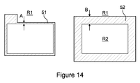
- Figure 14 shows a comparison between a voltage isolation structure according to an embodiment 51, and a prior art voltage isolation arrangement 52, in which a drift isolation region is used to provide lateral isolation.
- Both voltage isolation structures are designed to handle 700V, and the width A of the isolation structure 51 according to an embodiment is approximately 35 microns, compared with a width B of 130 microns for a drift isolation region 52.
- the die area for the isolation structure is therefore much smaller when an embodiment of the present invention is used.
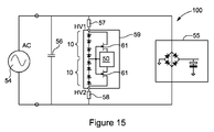
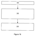
- FIG. 15 shows an illustrative application of a semiconductor structure according to an embodiment of the invention.
- An electronic apparatus 100 comprising an AC-DC converter 55, connected to an AC power supply 54.
- the AC power supply may supply 230V RMS alternating current, having a peak to peak voltage of approximately 320V.
- a filter capacitor 56 (sometimes referred to as an x-capacitor) is connected in parallel with the AC power supply 54, to shunt high frequencies from the AC power supply 54 before they reach the AC-DC convertor 55.
- the filter capacitor 56 handles mains voltages and is a potential safety risk to a person performing maintenance or repair on the apparatus 100. Even when AC power source is disconnected the filter capacitor 56 may store a hazardous voltage.
- a capacitor discharge circuit 59 may be provided to discharge the filter capacitor 56.
- Such capacitor discharge circuits are conventionally protected from high voltage transients by an external passive component, such as a metal oxide varistor. Such external devices are relatively large, and occupy a significant amount of circuit board space.
- the capacitor discharge circuit 59 includes an integrated over-voltage protection, comprising two semiconductor structures 10 that are each embodiments of the first aspect of the invention.
- the semiconductor structures 10 each comprise a series arrangement of four Zener diodes, arranged to limit the voltage on the transistors 61 and their associated control circuit 50. Further resistors 57 and 58 are provided in series with the semiconductor structures 10 to limit the current through the semiconductor structures 10 during an overvoltage event.
- Semiconductor structures according to embodiments of the invention may be integrated on the same die as the transistors 61 and their associated control circuit 50, and the resistors 57 and 58 may also be included. Such an arrangement provides a more compact and lower cost arrangement than prior art devices, which require an external component to provide over-voltage protection to the capacitor discharge circuit 59.
- semiconductor structures 10 in accordance with the invention may be applied to a range of other electronic apparatus, with similar benefits.
- a semiconductor layer is provided (e.g. a bulk silicon, or a semiconductor on insulator layer).
- a voltage isolator is defined in the semiconductor layer, by forming a series of insulating regions. An intermediate region of the semiconductor layer is defined between each pair of adjacent insulating region, and a first semiconductor region is thereby defined outside the voltage isolator and a second semiconductor region is thereby defined within the voltage isolator.
- a voltage control device is defined, comprising a conducting element connected to at least one intermediate semiconductor region, in parallel with at least one insulating region.
Landscapes
- Element Separation (AREA)
- Semiconductor Integrated Circuits (AREA)
- Engineering & Computer Science (AREA)
- Physics & Mathematics (AREA)
- Condensed Matter Physics & Semiconductors (AREA)
- General Physics & Mathematics (AREA)
- Manufacturing & Machinery (AREA)
- Computer Hardware Design (AREA)
- Microelectronics & Electronic Packaging (AREA)
- Power Engineering (AREA)
Claims (15)
- Eine Halbleiter Struktur aufweisend:einen ersten Halbleiter Bereich,einen zweiten Halbleiter Bereich innerhalb des ersten Halbleiter Bereichs undeinen Spannungsisolator, welcher den ersten Halbleiter Bereich und den zweiten Halbleiter Bereich voneinander trennt, wobei der Spannungsisolator aufweist:eine verschachtelte Serie von isolierenden Bereichen um den Umfang von dem zweiten Halbleiter Bereich herum,einen intermediären Halbleiter Bereich zwischen jedem angrenzenden Paar von verschachtelten isolierenden Bereichen undeine Spannung Steuervorrichtung, welche ein leitfähiges Element aufweist, welches an zumindest einen intermediären Halbleiter Bereich parallel mit dem zumindest einen isolierenden Bereich verbunden ist, um so eine Spannung über den zumindest einen isolierenden Bereich zu steuern.
- Die Struktur gemäß Anspruch 1, wobei die Spannung Steuervorrichtung ein leitfähiges Element aufweist, welches parallel mit jedem isolierenden Bereich verbunden ist, um so die Spannung über jeden isolierenden Bereich zu steuern.
- Die Struktur gemäß Anspruch 2, wobei die Spannung Steuervorrichtung eine Mehrzahl von leitfähigen Elementen aufweist, welche in Reihe verbunden sind,
wobei jedes leitfähige Element parallel mit einem korrespondierenden isolierenden Bereich verbunden ist,
wobei die Spannung Steuervorrichtung verbunden ist
an einer ersten Stelle an den ersten Bereich,
an einer zweiten Stelle an den zweiten Bereich,
und intermediäre Verbindungen hat zwischen der ersten Lokalität und der zweiten Lokalität zu jedem intermediären Halbleiter Bereich. - Die Struktur gemäß einem beliebigen vorhergehenden Anspruch, wobei die Spannung Steuervorrichtung zumindest teilweise definiert ist in zumindest einem von: dem ersten Halbleiter Bereich, einem intermediären Halbleiter Bereich und dem zweiten Halbleiter Bereich.
- Die Struktur gemäß einem beliebigen vorhergehenden Anspruch, wobei der erste Halbleiter Bereich und der zweite Halbleiter Bereich in derselben Halbleiter Schicht definiert sind.
- Die Struktur gemäß Anspruch 5, wobei die Halbleiter Schicht eine Silizium-auf-Isolator Schicht oder eine Halbleiter-auf-Isolator Schicht aufweist.
- Die Struktur gemäß Anspruch 5 oder 6, wobei jeder nicht-leitfähige Bereich eine Graben Isolationsstruktur aufweist.
- Die Struktur gemäß Anspruch 7, wobei die Graben Isolationsstruktur durch eine volle Dicke von der Halbleiter Schicht ist.
- Die Struktur gemäß Anspruch 3, wobei jedes leitfähige Element einen Widerstand aufweist.
- Die Struktur gemäß einem beliebigen von den Ansprüchen 1 bis 9, wobei jedes leitfähige Element eine Diode oder eine Mehrzahl von Dioden, welche in Reihe verbunden sind, aufweist.
- Die Struktur gemäß Anspruch 10, wobei die Diode oder jede Diode eine Zener Diode aufweist.
- Eine Halbleiter Vorrichtung, welche die Halbleiter Struktur gemäß Anspruch 11 aufweist, wobei die Halbleiter Struktur konfiguriert ist als: eine Hochspannung Zener Diode oder eine Hochspannung Klemme.
- Ein elektronischer Apparat, welche die Halbleiter Vorrichtung gemäß Anspruch 12 aufweist.
- Der Apparat gemäß Anspruch 13, wobei der Apparat einen integrierten Schaltkreis aufweist zum Entladen eines Netz-filternden Kondensators und
die Halbleiter Vorrichtung konfiguriert ist zum Schützen des integrierten Schaltkreises vor Überspannungsschaden, welcher von Netz-Überspannung verursacht ist. - Ein Verfahren zum Herstellen der Halbleiter Struktur gemäß einem beliebigen von den Ansprüchen 1 bis 11, aufweisend:Bereitstellen einer Halbleiter Schicht;Definieren eines ersten Halbleiter Bereichs und eines zweiten Halbleiter Bereichs von der Halbleiter Schicht mittels Bildens eines Spannungsisolators um einen Umfang von dem zweiten Halbleiter Bereich herum,
Trennens von ihm von dem ersten Halbleiter Bereich,
wobei der Spannungsisolator eine verschachtelte Serie von isolierenden Bereichen aufweist, wobei ein intermediärer Bereich von der Halbleiter Schicht zwischen jedem angrenzenden Paar von isolierenden Bereichen ist;Definieren einer Spannung Steuervorrichtung, welche ein leitfähiges Element aufweist, welches an zumindest einen intermediären Halbleiter Bereich parallel mit zumindest einem isolierenden Bereich verbunden ist, um so eine Spannung über den zumindest einen isolierenden Bereich zu steuern.
Priority Applications (3)
| Application Number | Priority Date | Filing Date | Title |
|---|---|---|---|
| EP14164475.7A EP2930743B1 (de) | 2014-04-11 | 2014-04-11 | Halbleiterisolationsstruktur |
| US14/672,601 US9543288B2 (en) | 2014-04-11 | 2015-03-30 | Semiconductor isolation structure |
| CN201510163237.6A CN104979343B (zh) | 2014-04-11 | 2015-04-08 | 半导体隔离结构 |
Applications Claiming Priority (1)
| Application Number | Priority Date | Filing Date | Title |
|---|---|---|---|
| EP14164475.7A EP2930743B1 (de) | 2014-04-11 | 2014-04-11 | Halbleiterisolationsstruktur |
Publications (2)
| Publication Number | Publication Date |
|---|---|
| EP2930743A1 EP2930743A1 (de) | 2015-10-14 |
| EP2930743B1 true EP2930743B1 (de) | 2016-09-21 |
Family
ID=50473200
Family Applications (1)
| Application Number | Title | Priority Date | Filing Date |
|---|---|---|---|
| EP14164475.7A Active EP2930743B1 (de) | 2014-04-11 | 2014-04-11 | Halbleiterisolationsstruktur |
Country Status (3)
| Country | Link |
|---|---|
| US (1) | US9543288B2 (de) |
| EP (1) | EP2930743B1 (de) |
| CN (1) | CN104979343B (de) |
Families Citing this family (2)
| Publication number | Priority date | Publication date | Assignee | Title |
|---|---|---|---|---|
| DE102019103730B4 (de) * | 2019-02-14 | 2021-02-04 | Infineon Technologies Austria Ag | Schaltungsanordnung mit galvanischer isolation zwischen elektronischen schaltungen |
| GB202001477D0 (en) | 2020-02-04 | 2020-03-18 | Search For The Next Ltd | A structure and method for guarding a low voltage region of a semiconductor device from a high voltage region of the semiconductor device |
Family Cites Families (10)
| Publication number | Priority date | Publication date | Assignee | Title |
|---|---|---|---|---|
| JP4030257B2 (ja) * | 2000-08-14 | 2008-01-09 | 株式会社ルネサステクノロジ | 半導体集積回路装置 |
| JP4471480B2 (ja) * | 2000-10-18 | 2010-06-02 | 三菱電機株式会社 | 半導体装置 |
| JP2002246551A (ja) * | 2001-02-15 | 2002-08-30 | Hitachi Ltd | 半導体装置 |
| US6664608B1 (en) * | 2001-11-30 | 2003-12-16 | Sun Microsystems, Inc. | Back-biased MOS device |
| US7179691B1 (en) * | 2002-07-29 | 2007-02-20 | Taiwan Semiconductor Manufacturing Co., Ltd. | Method for four direction low capacitance ESD protection |
| TW586124B (en) * | 2002-09-18 | 2004-05-01 | Macronix Int Co Ltd | ESD protection apparatus and method for a high-voltage input pad |
| JP2007201220A (ja) * | 2006-01-27 | 2007-08-09 | Mitsubishi Electric Corp | 半導体装置 |
| JP5499915B2 (ja) | 2009-06-10 | 2014-05-21 | 富士電機株式会社 | 高耐圧半導体装置 |
| CN102683262A (zh) * | 2012-04-28 | 2012-09-19 | 东南大学 | 一种基于绝缘体上硅的高压隔离结构 |
| US20140001567A1 (en) * | 2012-06-28 | 2014-01-02 | Skyworks Solutions, Inc. | Fet transistor on high-resistivity substrate |
-
2014
- 2014-04-11 EP EP14164475.7A patent/EP2930743B1/de active Active
-
2015
- 2015-03-30 US US14/672,601 patent/US9543288B2/en active Active
- 2015-04-08 CN CN201510163237.6A patent/CN104979343B/zh active Active
Also Published As
| Publication number | Publication date |
|---|---|
| CN104979343A (zh) | 2015-10-14 |
| US9543288B2 (en) | 2017-01-10 |
| CN104979343B (zh) | 2018-06-01 |
| EP2930743A1 (de) | 2015-10-14 |
| US20150294965A1 (en) | 2015-10-15 |
Similar Documents
| Publication | Publication Date | Title |
|---|---|---|
| US7709908B2 (en) | High-voltage MOS transistor device | |
| US10978441B2 (en) | Transient voltage suppressor and method for manufacturing the same | |
| CN103378097B (zh) | 系统级esd保护的共享堆叠bjt钳位 | |
| US10157904B2 (en) | High surge bi-directional transient voltage suppressor | |
| US9831232B2 (en) | ESD protection device | |
| US8963277B2 (en) | Semiconductor structure and method of manufacturing the same | |
| US10483257B2 (en) | Low voltage NPN with low trigger voltage and high snap back voltage for ESD protection | |
| US20150002967A1 (en) | Semiconductor device | |
| CN101937925B (zh) | 一种半导体器件 | |
| WO2012065229A1 (en) | Single-chip integrated circuit with capacitive isolation | |
| US20200243504A1 (en) | Rectification device having a forward pn junction and a reverse schottky barrier formed in an epitaxial semiconductor layer formed over a semiconductor substrate | |
| US10211058B2 (en) | ESD protection device | |
| US20170025402A1 (en) | Semiconductor esd protection circuit | |
| EP2718972A1 (de) | Superhochspannungswiderstand auf silizium | |
| KR102872597B1 (ko) | 비대칭 항복 전압을 갖는 tvs 다이오드 및 어셈블리 | |
| EP3593432B1 (de) | Hybride überspannungsschutzvorrichtung und anordnung | |
| EP2930743B1 (de) | Halbleiterisolationsstruktur | |
| US20150311701A1 (en) | Method and system for transient voltage suppression devices with active control | |
| EP2876686B1 (de) | Hochspannungs-Halbleitervorrichtung und Verfahren zu deren Herstellung | |
| EP3192102A1 (de) | Halbleiterbauelement mit einer diode und vorrichtung zum schutz vor elektrostatischer entladung | |
| JP2015179776A (ja) | 半導体装置 | |
| US20220238508A1 (en) | Vertical device having a reverse schottky barrier formed in an epitaxial semiconductor layer formed over a semiconductor substrate | |
| EP2947691B1 (de) | Halbleiterbauelement | |
| JP2013207047A (ja) | 半導体装置 | |
| HK40055473A (en) | Top hat structure for isolation capacitors |
Legal Events
| Date | Code | Title | Description |
|---|---|---|---|
| PUAI | Public reference made under article 153(3) epc to a published international application that has entered the european phase |
Free format text: ORIGINAL CODE: 0009012 |
|
| AK | Designated contracting states |
Kind code of ref document: A1 Designated state(s): AL AT BE BG CH CY CZ DE DK EE ES FI FR GB GR HR HU IE IS IT LI LT LU LV MC MK MT NL NO PL PT RO RS SE SI SK SM TR |
|
| AX | Request for extension of the european patent |
Extension state: BA ME |
|
| 17P | Request for examination filed |
Effective date: 20160414 |
|
| RBV | Designated contracting states (corrected) |
Designated state(s): AL AT BE BG CH CY CZ DE DK EE ES FI FR GB GR HR HU IE IS IT LI LT LU LV MC MK MT NL NO PL PT RO RS SE SI SK SM TR |
|
| GRAJ | Information related to disapproval of communication of intention to grant by the applicant or resumption of examination proceedings by the epo deleted |
Free format text: ORIGINAL CODE: EPIDOSDIGR1 |
|
| GRAP | Despatch of communication of intention to grant a patent |
Free format text: ORIGINAL CODE: EPIDOSNIGR1 |
|
| RIC1 | Information provided on ipc code assigned before grant |
Ipc: H01L 21/76 20060101AFI20160527BHEP Ipc: H01L 21/8238 20060101ALI20160527BHEP Ipc: H01L 27/02 20060101ALI20160527BHEP |
|
| INTG | Intention to grant announced |
Effective date: 20160623 |
|
| RIN1 | Information on inventor provided before grant (corrected) |
Inventor name: STRIJKER, JOAN, W Inventor name: EMMERIK-WEIJLAND, INESZ,M |
|
| GRAS | Grant fee paid |
Free format text: ORIGINAL CODE: EPIDOSNIGR3 |
|
| GRAA | (expected) grant |
Free format text: ORIGINAL CODE: 0009210 |
|
| AK | Designated contracting states |
Kind code of ref document: B1 Designated state(s): AL AT BE BG CH CY CZ DE DK EE ES FI FR GB GR HR HU IE IS IT LI LT LU LV MC MK MT NL NO PL PT RO RS SE SI SK SM TR |
|
| REG | Reference to a national code |
Ref country code: GB Ref legal event code: FG4D |
|
| REG | Reference to a national code |
Ref country code: CH Ref legal event code: EP |
|
| REG | Reference to a national code |
Ref country code: AT Ref legal event code: REF Ref document number: 831652 Country of ref document: AT Kind code of ref document: T Effective date: 20161015 |
|
| REG | Reference to a national code |
Ref country code: IE Ref legal event code: FG4D |
|
| REG | Reference to a national code |
Ref country code: DE Ref legal event code: R096 Ref document number: 602014003740 Country of ref document: DE |
|
| REG | Reference to a national code |
Ref country code: LT Ref legal event code: MG4D Ref country code: NL Ref legal event code: MP Effective date: 20160921 |
|
| PG25 | Lapsed in a contracting state [announced via postgrant information from national office to epo] |
Ref country code: FI Free format text: LAPSE BECAUSE OF FAILURE TO SUBMIT A TRANSLATION OF THE DESCRIPTION OR TO PAY THE FEE WITHIN THE PRESCRIBED TIME-LIMIT Effective date: 20160921 Ref country code: LT Free format text: LAPSE BECAUSE OF FAILURE TO SUBMIT A TRANSLATION OF THE DESCRIPTION OR TO PAY THE FEE WITHIN THE PRESCRIBED TIME-LIMIT Effective date: 20160921 Ref country code: HR Free format text: LAPSE BECAUSE OF FAILURE TO SUBMIT A TRANSLATION OF THE DESCRIPTION OR TO PAY THE FEE WITHIN THE PRESCRIBED TIME-LIMIT Effective date: 20160921 Ref country code: RS Free format text: LAPSE BECAUSE OF FAILURE TO SUBMIT A TRANSLATION OF THE DESCRIPTION OR TO PAY THE FEE WITHIN THE PRESCRIBED TIME-LIMIT Effective date: 20160921 Ref country code: NO Free format text: LAPSE BECAUSE OF FAILURE TO SUBMIT A TRANSLATION OF THE DESCRIPTION OR TO PAY THE FEE WITHIN THE PRESCRIBED TIME-LIMIT Effective date: 20161221 |
|
| REG | Reference to a national code |
Ref country code: AT Ref legal event code: MK05 Ref document number: 831652 Country of ref document: AT Kind code of ref document: T Effective date: 20160921 |
|
| PG25 | Lapsed in a contracting state [announced via postgrant information from national office to epo] |
Ref country code: GR Free format text: LAPSE BECAUSE OF FAILURE TO SUBMIT A TRANSLATION OF THE DESCRIPTION OR TO PAY THE FEE WITHIN THE PRESCRIBED TIME-LIMIT Effective date: 20161222 Ref country code: SE Free format text: LAPSE BECAUSE OF FAILURE TO SUBMIT A TRANSLATION OF THE DESCRIPTION OR TO PAY THE FEE WITHIN THE PRESCRIBED TIME-LIMIT Effective date: 20160921 Ref country code: LV Free format text: LAPSE BECAUSE OF FAILURE TO SUBMIT A TRANSLATION OF THE DESCRIPTION OR TO PAY THE FEE WITHIN THE PRESCRIBED TIME-LIMIT Effective date: 20160921 Ref country code: NL Free format text: LAPSE BECAUSE OF FAILURE TO SUBMIT A TRANSLATION OF THE DESCRIPTION OR TO PAY THE FEE WITHIN THE PRESCRIBED TIME-LIMIT Effective date: 20160921 |
|
| REG | Reference to a national code |
Ref country code: FR Ref legal event code: PLFP Year of fee payment: 4 |
|
| PG25 | Lapsed in a contracting state [announced via postgrant information from national office to epo] |
Ref country code: RO Free format text: LAPSE BECAUSE OF FAILURE TO SUBMIT A TRANSLATION OF THE DESCRIPTION OR TO PAY THE FEE WITHIN THE PRESCRIBED TIME-LIMIT Effective date: 20160921 Ref country code: EE Free format text: LAPSE BECAUSE OF FAILURE TO SUBMIT A TRANSLATION OF THE DESCRIPTION OR TO PAY THE FEE WITHIN THE PRESCRIBED TIME-LIMIT Effective date: 20160921 |
|
| PG25 | Lapsed in a contracting state [announced via postgrant information from national office to epo] |
Ref country code: PL Free format text: LAPSE BECAUSE OF FAILURE TO SUBMIT A TRANSLATION OF THE DESCRIPTION OR TO PAY THE FEE WITHIN THE PRESCRIBED TIME-LIMIT Effective date: 20160921 Ref country code: AT Free format text: LAPSE BECAUSE OF FAILURE TO SUBMIT A TRANSLATION OF THE DESCRIPTION OR TO PAY THE FEE WITHIN THE PRESCRIBED TIME-LIMIT Effective date: 20160921 Ref country code: SM Free format text: LAPSE BECAUSE OF FAILURE TO SUBMIT A TRANSLATION OF THE DESCRIPTION OR TO PAY THE FEE WITHIN THE PRESCRIBED TIME-LIMIT Effective date: 20160921 Ref country code: ES Free format text: LAPSE BECAUSE OF FAILURE TO SUBMIT A TRANSLATION OF THE DESCRIPTION OR TO PAY THE FEE WITHIN THE PRESCRIBED TIME-LIMIT Effective date: 20160921 Ref country code: IS Free format text: LAPSE BECAUSE OF FAILURE TO SUBMIT A TRANSLATION OF THE DESCRIPTION OR TO PAY THE FEE WITHIN THE PRESCRIBED TIME-LIMIT Effective date: 20170121 Ref country code: SK Free format text: LAPSE BECAUSE OF FAILURE TO SUBMIT A TRANSLATION OF THE DESCRIPTION OR TO PAY THE FEE WITHIN THE PRESCRIBED TIME-LIMIT Effective date: 20160921 Ref country code: BG Free format text: LAPSE BECAUSE OF FAILURE TO SUBMIT A TRANSLATION OF THE DESCRIPTION OR TO PAY THE FEE WITHIN THE PRESCRIBED TIME-LIMIT Effective date: 20161221 Ref country code: BE Free format text: LAPSE BECAUSE OF FAILURE TO SUBMIT A TRANSLATION OF THE DESCRIPTION OR TO PAY THE FEE WITHIN THE PRESCRIBED TIME-LIMIT Effective date: 20160921 Ref country code: CZ Free format text: LAPSE BECAUSE OF FAILURE TO SUBMIT A TRANSLATION OF THE DESCRIPTION OR TO PAY THE FEE WITHIN THE PRESCRIBED TIME-LIMIT Effective date: 20160921 Ref country code: PT Free format text: LAPSE BECAUSE OF FAILURE TO SUBMIT A TRANSLATION OF THE DESCRIPTION OR TO PAY THE FEE WITHIN THE PRESCRIBED TIME-LIMIT Effective date: 20170123 |
|
| REG | Reference to a national code |
Ref country code: DE Ref legal event code: R097 Ref document number: 602014003740 Country of ref document: DE |
|
| PG25 | Lapsed in a contracting state [announced via postgrant information from national office to epo] |
Ref country code: IT Free format text: LAPSE BECAUSE OF FAILURE TO SUBMIT A TRANSLATION OF THE DESCRIPTION OR TO PAY THE FEE WITHIN THE PRESCRIBED TIME-LIMIT Effective date: 20160921 |
|
| PLBE | No opposition filed within time limit |
Free format text: ORIGINAL CODE: 0009261 |
|
| STAA | Information on the status of an ep patent application or granted ep patent |
Free format text: STATUS: NO OPPOSITION FILED WITHIN TIME LIMIT |
|
| PG25 | Lapsed in a contracting state [announced via postgrant information from national office to epo] |
Ref country code: DK Free format text: LAPSE BECAUSE OF FAILURE TO SUBMIT A TRANSLATION OF THE DESCRIPTION OR TO PAY THE FEE WITHIN THE PRESCRIBED TIME-LIMIT Effective date: 20160921 |
|
| 26N | No opposition filed |
Effective date: 20170622 |
|
| PG25 | Lapsed in a contracting state [announced via postgrant information from national office to epo] |
Ref country code: SI Free format text: LAPSE BECAUSE OF FAILURE TO SUBMIT A TRANSLATION OF THE DESCRIPTION OR TO PAY THE FEE WITHIN THE PRESCRIBED TIME-LIMIT Effective date: 20160921 |
|
| REG | Reference to a national code |
Ref country code: CH Ref legal event code: PL |
|
| REG | Reference to a national code |
Ref country code: IE Ref legal event code: MM4A |
|
| PG25 | Lapsed in a contracting state [announced via postgrant information from national office to epo] |
Ref country code: MC Free format text: LAPSE BECAUSE OF FAILURE TO SUBMIT A TRANSLATION OF THE DESCRIPTION OR TO PAY THE FEE WITHIN THE PRESCRIBED TIME-LIMIT Effective date: 20160921 |
|
| PG25 | Lapsed in a contracting state [announced via postgrant information from national office to epo] |
Ref country code: LU Free format text: LAPSE BECAUSE OF NON-PAYMENT OF DUE FEES Effective date: 20170411 Ref country code: CH Free format text: LAPSE BECAUSE OF NON-PAYMENT OF DUE FEES Effective date: 20170430 Ref country code: LI Free format text: LAPSE BECAUSE OF NON-PAYMENT OF DUE FEES Effective date: 20170430 |
|
| REG | Reference to a national code |
Ref country code: FR Ref legal event code: PLFP Year of fee payment: 5 |
|
| PG25 | Lapsed in a contracting state [announced via postgrant information from national office to epo] |
Ref country code: IE Free format text: LAPSE BECAUSE OF NON-PAYMENT OF DUE FEES Effective date: 20170411 |
|
| PG25 | Lapsed in a contracting state [announced via postgrant information from national office to epo] |
Ref country code: MT Free format text: LAPSE BECAUSE OF NON-PAYMENT OF DUE FEES Effective date: 20170411 |
|
| PG25 | Lapsed in a contracting state [announced via postgrant information from national office to epo] |
Ref country code: AL Free format text: LAPSE BECAUSE OF FAILURE TO SUBMIT A TRANSLATION OF THE DESCRIPTION OR TO PAY THE FEE WITHIN THE PRESCRIBED TIME-LIMIT Effective date: 20160921 |
|
| PG25 | Lapsed in a contracting state [announced via postgrant information from national office to epo] |
Ref country code: HU Free format text: LAPSE BECAUSE OF FAILURE TO SUBMIT A TRANSLATION OF THE DESCRIPTION OR TO PAY THE FEE WITHIN THE PRESCRIBED TIME-LIMIT; INVALID AB INITIO Effective date: 20140411 |
|
| PG25 | Lapsed in a contracting state [announced via postgrant information from national office to epo] |
Ref country code: CY Free format text: LAPSE BECAUSE OF FAILURE TO SUBMIT A TRANSLATION OF THE DESCRIPTION OR TO PAY THE FEE WITHIN THE PRESCRIBED TIME-LIMIT Effective date: 20160921 |
|
| PG25 | Lapsed in a contracting state [announced via postgrant information from national office to epo] |
Ref country code: MK Free format text: LAPSE BECAUSE OF FAILURE TO SUBMIT A TRANSLATION OF THE DESCRIPTION OR TO PAY THE FEE WITHIN THE PRESCRIBED TIME-LIMIT Effective date: 20160921 |
|
| PG25 | Lapsed in a contracting state [announced via postgrant information from national office to epo] |
Ref country code: TR Free format text: LAPSE BECAUSE OF FAILURE TO SUBMIT A TRANSLATION OF THE DESCRIPTION OR TO PAY THE FEE WITHIN THE PRESCRIBED TIME-LIMIT Effective date: 20160921 |
|
| P01 | Opt-out of the competence of the unified patent court (upc) registered |
Effective date: 20230725 |
|
| PGFP | Annual fee paid to national office [announced via postgrant information from national office to epo] |
Ref country code: FR Payment date: 20250319 Year of fee payment: 12 |
|
| PGFP | Annual fee paid to national office [announced via postgrant information from national office to epo] |
Ref country code: GB Payment date: 20250319 Year of fee payment: 12 |
|
| PGFP | Annual fee paid to national office [announced via postgrant information from national office to epo] |
Ref country code: DE Payment date: 20250319 Year of fee payment: 12 |
|
| REG | Reference to a national code |
Ref country code: DE Ref legal event code: R079 Ref document number: 602014003740 Country of ref document: DE Free format text: PREVIOUS MAIN CLASS: H01L0021760000 Ipc: H10W0010000000 |