EP2930213B1 - Curable silicone composition and optical semiconductor device - Google Patents
Curable silicone composition and optical semiconductor device Download PDFInfo
- Publication number
- EP2930213B1 EP2930213B1 EP13860333.7A EP13860333A EP2930213B1 EP 2930213 B1 EP2930213 B1 EP 2930213B1 EP 13860333 A EP13860333 A EP 13860333A EP 2930213 B1 EP2930213 B1 EP 2930213B1
- Authority
- EP
- European Patent Office
- Prior art keywords
- group
- optical semiconductor
- component
- groups
- curable silicone
- Prior art date
- Legal status (The legal status is an assumption and is not a legal conclusion. Google has not performed a legal analysis and makes no representation as to the accuracy of the status listed.)
- Active
Links
- 239000000203 mixture Substances 0.000 title claims description 78
- 229920001296 polysiloxane Polymers 0.000 title claims description 65
- 230000003287 optical effect Effects 0.000 title claims description 51
- 239000004065 semiconductor Substances 0.000 title claims description 51
- XLOMVQKBTHCTTD-UHFFFAOYSA-N Zinc monoxide Chemical compound [Zn]=O XLOMVQKBTHCTTD-UHFFFAOYSA-N 0.000 claims description 48
- -1 triazole compound Chemical class 0.000 claims description 37
- 229910052709 silver Inorganic materials 0.000 claims description 26
- 239000000843 powder Substances 0.000 claims description 25
- 125000004435 hydrogen atom Chemical group [H]* 0.000 claims description 24
- 239000011787 zinc oxide Substances 0.000 claims description 24
- 125000003342 alkenyl group Chemical group 0.000 claims description 23
- 239000002245 particle Substances 0.000 claims description 15
- 238000006459 hydrosilylation reaction Methods 0.000 claims description 14
- 229910052782 aluminium Inorganic materials 0.000 claims description 9
- 150000003961 organosilicon compounds Chemical class 0.000 claims description 9
- 239000007809 chemical reaction catalyst Substances 0.000 claims description 8
- 238000010438 heat treatment Methods 0.000 claims description 7
- 229910052710 silicon Inorganic materials 0.000 claims description 7
- 229910020485 SiO4/2 Inorganic materials 0.000 claims description 6
- XLYOFNOQVPJJNP-UHFFFAOYSA-M hydroxide Chemical compound [OH-] XLYOFNOQVPJJNP-UHFFFAOYSA-M 0.000 claims description 6
- 238000007789 sealing Methods 0.000 claims description 6
- 229910020388 SiO1/2 Inorganic materials 0.000 claims description 5
- 229910052761 rare earth metal Inorganic materials 0.000 claims description 5
- 229910052802 copper Inorganic materials 0.000 claims description 4
- 229920006136 organohydrogenpolysiloxane Polymers 0.000 claims description 4
- 229910020487 SiO3/2 Inorganic materials 0.000 claims description 3
- 229910052787 antimony Inorganic materials 0.000 claims description 3
- 229910052742 iron Inorganic materials 0.000 claims description 3
- 229910052718 tin Inorganic materials 0.000 claims description 3
- 229910052719 titanium Inorganic materials 0.000 claims description 3
- 229910052726 zirconium Inorganic materials 0.000 claims description 3
- 229910020447 SiO2/2 Inorganic materials 0.000 claims description 2
- 239000002683 reaction inhibitor Substances 0.000 claims description 2
- 125000001183 hydrocarbyl group Chemical group 0.000 claims 2
- 239000012299 nitrogen atmosphere Substances 0.000 claims 1
- BQCADISMDOOEFD-UHFFFAOYSA-N Silver Chemical compound [Ag] BQCADISMDOOEFD-UHFFFAOYSA-N 0.000 description 23
- 239000004332 silver Substances 0.000 description 23
- 239000000126 substance Substances 0.000 description 23
- 125000000391 vinyl group Chemical group [H]C([*])=C([H])[H] 0.000 description 17
- VYPSYNLAJGMNEJ-UHFFFAOYSA-N Silicium dioxide Chemical compound O=[Si]=O VYPSYNLAJGMNEJ-UHFFFAOYSA-N 0.000 description 16
- BASFCYQUMIYNBI-UHFFFAOYSA-N platinum Chemical compound [Pt] BASFCYQUMIYNBI-UHFFFAOYSA-N 0.000 description 16
- 239000000758 substrate Substances 0.000 description 14
- NINIDFKCEFEMDL-UHFFFAOYSA-N Sulfur Chemical compound [S] NINIDFKCEFEMDL-UHFFFAOYSA-N 0.000 description 13
- 229910052717 sulfur Inorganic materials 0.000 description 13
- 239000011593 sulfur Substances 0.000 description 13
- YXFVVABEGXRONW-UHFFFAOYSA-N Toluene Chemical compound CC1=CC=CC=C1 YXFVVABEGXRONW-UHFFFAOYSA-N 0.000 description 12
- 238000002845 discoloration Methods 0.000 description 12
- 238000007747 plating Methods 0.000 description 11
- 239000007789 gas Substances 0.000 description 10
- 238000003860 storage Methods 0.000 description 10
- 229920001577 copolymer Polymers 0.000 description 9
- 150000002430 hydrocarbons Chemical group 0.000 description 9
- 239000003054 catalyst Substances 0.000 description 8
- 239000000377 silicon dioxide Substances 0.000 description 8
- 238000003878 thermal aging Methods 0.000 description 8
- XUIMIQQOPSSXEZ-UHFFFAOYSA-N Silicon Chemical group [Si] XUIMIQQOPSSXEZ-UHFFFAOYSA-N 0.000 description 7
- 229910052681 coesite Inorganic materials 0.000 description 7
- 229910052906 cristobalite Inorganic materials 0.000 description 7
- 239000000463 material Substances 0.000 description 7
- 125000002496 methyl group Chemical group [H]C([H])([H])* 0.000 description 7
- 229910052697 platinum Inorganic materials 0.000 description 7
- 229920001843 polymethylhydrosiloxane Polymers 0.000 description 7
- 229910052682 stishovite Inorganic materials 0.000 description 7
- 229910052905 tridymite Inorganic materials 0.000 description 7
- 229910052693 Europium Inorganic materials 0.000 description 6
- 239000002253 acid Substances 0.000 description 6
- 125000000217 alkyl group Chemical group 0.000 description 6
- WNROFYMDJYEPJX-UHFFFAOYSA-K aluminium hydroxide Chemical compound [OH-].[OH-].[OH-].[Al+3] WNROFYMDJYEPJX-UHFFFAOYSA-K 0.000 description 6
- 229910021502 aluminium hydroxide Inorganic materials 0.000 description 6
- PNEYBMLMFCGWSK-UHFFFAOYSA-N aluminium oxide Inorganic materials [O-2].[O-2].[O-2].[Al+3].[Al+3] PNEYBMLMFCGWSK-UHFFFAOYSA-N 0.000 description 6
- 229910001679 gibbsite Inorganic materials 0.000 description 6
- 239000007787 solid Substances 0.000 description 6
- 229910052684 Cerium Inorganic materials 0.000 description 5
- XAGFODPZIPBFFR-UHFFFAOYSA-N aluminium Chemical compound [Al] XAGFODPZIPBFFR-UHFFFAOYSA-N 0.000 description 5
- 125000003710 aryl alkyl group Chemical group 0.000 description 5
- 125000003118 aryl group Chemical group 0.000 description 5
- BITPLIXHRASDQB-UHFFFAOYSA-N ethenyl-[ethenyl(dimethyl)silyl]oxy-dimethylsilane Chemical compound C=C[Si](C)(C)O[Si](C)(C)C=C BITPLIXHRASDQB-UHFFFAOYSA-N 0.000 description 5
- 230000004907 flux Effects 0.000 description 5
- 239000007788 liquid Substances 0.000 description 5
- 125000001997 phenyl group Chemical group [H]C1=C([H])C([H])=C(*)C([H])=C1[H] 0.000 description 5
- QWENRTYMTSOGBR-UHFFFAOYSA-N 1H-1,2,3-Triazole Chemical compound C=1C=NNN=1 QWENRTYMTSOGBR-UHFFFAOYSA-N 0.000 description 4
- NSPMIYGKQJPBQR-UHFFFAOYSA-N 4H-1,2,4-triazole Chemical compound C=1N=CNN=1 NSPMIYGKQJPBQR-UHFFFAOYSA-N 0.000 description 4
- IJGRMHOSHXDMSA-UHFFFAOYSA-N Atomic nitrogen Chemical compound N#N IJGRMHOSHXDMSA-UHFFFAOYSA-N 0.000 description 4
- 238000005033 Fourier transform infrared spectroscopy Methods 0.000 description 4
- 238000005481 NMR spectroscopy Methods 0.000 description 4
- GWEVSGVZZGPLCZ-UHFFFAOYSA-N Titan oxide Chemical compound O=[Ti]=O GWEVSGVZZGPLCZ-UHFFFAOYSA-N 0.000 description 4
- MCMNRKCIXSYSNV-UHFFFAOYSA-N Zirconium dioxide Chemical compound O=[Zr]=O MCMNRKCIXSYSNV-UHFFFAOYSA-N 0.000 description 4
- 125000003545 alkoxy group Chemical group 0.000 description 4
- QRUDEWIWKLJBPS-UHFFFAOYSA-N benzotriazole Chemical compound C1=CC=C2N[N][N]C2=C1 QRUDEWIWKLJBPS-UHFFFAOYSA-N 0.000 description 4
- 239000012964 benzotriazole Substances 0.000 description 4
- 125000001246 bromo group Chemical group Br* 0.000 description 4
- 125000001309 chloro group Chemical group Cl* 0.000 description 4
- 229910052593 corundum Inorganic materials 0.000 description 4
- 125000001301 ethoxy group Chemical group [H]C([H])([H])C([H])([H])O* 0.000 description 4
- SZVJSHCCFOBDDC-UHFFFAOYSA-N ferrosoferric oxide Chemical compound O=[Fe]O[Fe]O[Fe]=O SZVJSHCCFOBDDC-UHFFFAOYSA-N 0.000 description 4
- 125000001153 fluoro group Chemical group F* 0.000 description 4
- 238000005227 gel permeation chromatography Methods 0.000 description 4
- 125000005843 halogen group Chemical group 0.000 description 4
- 150000004679 hydroxides Chemical class 0.000 description 4
- 125000000956 methoxy group Chemical group [H]C([H])([H])O* 0.000 description 4
- 229920005989 resin Polymers 0.000 description 4
- 239000011347 resin Substances 0.000 description 4
- 229910001845 yogo sapphire Inorganic materials 0.000 description 4
- VMAWODUEPLAHOE-UHFFFAOYSA-N 2,4,6,8-tetrakis(ethenyl)-2,4,6,8-tetramethyl-1,3,5,7,2,4,6,8-tetraoxatetrasilocane Chemical compound C=C[Si]1(C)O[Si](C)(C=C)O[Si](C)(C=C)O[Si](C)(C=C)O1 VMAWODUEPLAHOE-UHFFFAOYSA-N 0.000 description 3
- FMRLDPWIRHBCCC-UHFFFAOYSA-L Zinc carbonate Chemical compound [Zn+2].[O-]C([O-])=O FMRLDPWIRHBCCC-UHFFFAOYSA-L 0.000 description 3
- 239000002318 adhesion promoter Substances 0.000 description 3
- 125000001931 aliphatic group Chemical group 0.000 description 3
- GWXLDORMOJMVQZ-UHFFFAOYSA-N cerium Chemical compound [Ce] GWXLDORMOJMVQZ-UHFFFAOYSA-N 0.000 description 3
- 230000000052 comparative effect Effects 0.000 description 3
- 150000001875 compounds Chemical class 0.000 description 3
- 239000010949 copper Substances 0.000 description 3
- 230000007423 decrease Effects 0.000 description 3
- 239000004205 dimethyl polysiloxane Substances 0.000 description 3
- 235000013870 dimethyl polysiloxane Nutrition 0.000 description 3
- 125000005388 dimethylhydrogensiloxy group Chemical group 0.000 description 3
- 125000001495 ethyl group Chemical group [H]C([H])([H])C([H])([H])* 0.000 description 3
- 150000004677 hydrates Chemical class 0.000 description 3
- 229910052751 metal Inorganic materials 0.000 description 3
- 239000002184 metal Substances 0.000 description 3
- 229920000435 poly(dimethylsiloxane) Polymers 0.000 description 3
- 229930195735 unsaturated hydrocarbon Natural products 0.000 description 3
- 238000004383 yellowing Methods 0.000 description 3
- 229910052727 yttrium Inorganic materials 0.000 description 3
- VWQVUPCCIRVNHF-UHFFFAOYSA-N yttrium atom Chemical compound [Y] VWQVUPCCIRVNHF-UHFFFAOYSA-N 0.000 description 3
- 239000011667 zinc carbonate Substances 0.000 description 3
- 235000004416 zinc carbonate Nutrition 0.000 description 3
- 229910000010 zinc carbonate Inorganic materials 0.000 description 3
- QYLFHLNFIHBCPR-UHFFFAOYSA-N 1-ethynylcyclohexan-1-ol Chemical compound C#CC1(O)CCCCC1 QYLFHLNFIHBCPR-UHFFFAOYSA-N 0.000 description 2
- 125000000094 2-phenylethyl group Chemical group [H]C1=C([H])C([H])=C(C([H])=C1[H])C([H])([H])C([H])([H])* 0.000 description 2
- 125000003903 2-propenyl group Chemical group [H]C([*])([H])C([H])=C([H])[H] 0.000 description 2
- KLSJWNVTNUYHDU-UHFFFAOYSA-N Amitrole Chemical compound NC1=NC=NN1 KLSJWNVTNUYHDU-UHFFFAOYSA-N 0.000 description 2
- PXHVJJICTQNCMI-UHFFFAOYSA-N Nickel Chemical compound [Ni] PXHVJJICTQNCMI-UHFFFAOYSA-N 0.000 description 2
- KDLHZDBZIXYQEI-UHFFFAOYSA-N Palladium Chemical compound [Pd] KDLHZDBZIXYQEI-UHFFFAOYSA-N 0.000 description 2
- UCKMPCXJQFINFW-UHFFFAOYSA-N Sulphide Chemical compound [S-2] UCKMPCXJQFINFW-UHFFFAOYSA-N 0.000 description 2
- 239000007983 Tris buffer Substances 0.000 description 2
- 230000032683 aging Effects 0.000 description 2
- 238000004458 analytical method Methods 0.000 description 2
- 125000001797 benzyl group Chemical group [H]C1=C([H])C([H])=C(C([H])=C1[H])C([H])([H])* 0.000 description 2
- 125000000484 butyl group Chemical group [H]C([*])([H])C([H])([H])C([H])([H])C([H])([H])[H] 0.000 description 2
- CETPSERCERDGAM-UHFFFAOYSA-N ceric oxide Chemical compound O=[Ce]=O CETPSERCERDGAM-UHFFFAOYSA-N 0.000 description 2
- 229910000422 cerium(IV) oxide Inorganic materials 0.000 description 2
- 239000003795 chemical substances by application Substances 0.000 description 2
- 125000004122 cyclic group Chemical group 0.000 description 2
- 125000000113 cyclohexyl group Chemical group [H]C1([H])C([H])([H])C([H])([H])C([H])(*)C([H])([H])C1([H])[H] 0.000 description 2
- 125000002704 decyl group Chemical group [H]C([H])([H])C([H])([H])C([H])([H])C([H])([H])C([H])([H])C([H])([H])C([H])([H])C([H])([H])C([H])([H])C([H])([H])* 0.000 description 2
- 230000018044 dehydration Effects 0.000 description 2
- 238000006297 dehydration reaction Methods 0.000 description 2
- 125000003438 dodecyl group Chemical group [H]C([H])([H])C([H])([H])C([H])([H])C([H])([H])C([H])([H])C([H])([H])C([H])([H])C([H])([H])C([H])([H])C([H])([H])C([H])([H])C([H])([H])* 0.000 description 2
- 230000000694 effects Effects 0.000 description 2
- OGPBJKLSAFTDLK-UHFFFAOYSA-N europium atom Chemical compound [Eu] OGPBJKLSAFTDLK-UHFFFAOYSA-N 0.000 description 2
- 230000002349 favourable effect Effects 0.000 description 2
- PCHJSUWPFVWCPO-UHFFFAOYSA-N gold Chemical compound [Au] PCHJSUWPFVWCPO-UHFFFAOYSA-N 0.000 description 2
- 229910052737 gold Inorganic materials 0.000 description 2
- 239000010931 gold Substances 0.000 description 2
- 125000003187 heptyl group Chemical group [H]C([*])([H])C([H])([H])C([H])([H])C([H])([H])C([H])([H])C([H])([H])C([H])([H])[H] 0.000 description 2
- FFUAGWLWBBFQJT-UHFFFAOYSA-N hexamethyldisilazane Chemical compound C[Si](C)(C)N[Si](C)(C)C FFUAGWLWBBFQJT-UHFFFAOYSA-N 0.000 description 2
- 125000006038 hexenyl group Chemical group 0.000 description 2
- 125000004051 hexyl group Chemical group [H]C([H])([H])C([H])([H])C([H])([H])C([H])([H])C([H])([H])C([H])([H])* 0.000 description 2
- 125000002887 hydroxy group Chemical group [H]O* 0.000 description 2
- NYMPGSQKHIOWIO-UHFFFAOYSA-N hydroxy(diphenyl)silicon Chemical class C=1C=CC=CC=1[Si](O)C1=CC=CC=C1 NYMPGSQKHIOWIO-UHFFFAOYSA-N 0.000 description 2
- JEIPFZHSYJVQDO-UHFFFAOYSA-N iron(III) oxide Inorganic materials O=[Fe]O[Fe]=O JEIPFZHSYJVQDO-UHFFFAOYSA-N 0.000 description 2
- 125000000959 isobutyl group Chemical group [H]C([H])([H])C([H])(C([H])([H])[H])C([H])([H])* 0.000 description 2
- 125000001449 isopropyl group Chemical group [H]C([H])([H])C([H])(*)C([H])([H])[H] 0.000 description 2
- 238000005259 measurement Methods 0.000 description 2
- 150000002739 metals Chemical class 0.000 description 2
- 238000000034 method Methods 0.000 description 2
- 125000001624 naphthyl group Chemical group 0.000 description 2
- 125000001971 neopentyl group Chemical group [H]C([*])([H])C(C([H])([H])[H])(C([H])([H])[H])C([H])([H])[H] 0.000 description 2
- 150000004767 nitrides Chemical class 0.000 description 2
- 229910052757 nitrogen Inorganic materials 0.000 description 2
- 125000001400 nonyl group Chemical group [H]C([*])([H])C([H])([H])C([H])([H])C([H])([H])C([H])([H])C([H])([H])C([H])([H])C([H])([H])C([H])([H])[H] 0.000 description 2
- 125000002347 octyl group Chemical group [H]C([*])([H])C([H])([H])C([H])([H])C([H])([H])C([H])([H])C([H])([H])C([H])([H])C([H])([H])[H] 0.000 description 2
- 125000000962 organic group Chemical group 0.000 description 2
- 125000001147 pentyl group Chemical group C(CCCC)* 0.000 description 2
- 125000004344 phenylpropyl group Chemical group 0.000 description 2
- 239000000049 pigment Substances 0.000 description 2
- 125000001436 propyl group Chemical group [H]C([*])([H])C([H])([H])C([H])([H])[H] 0.000 description 2
- 238000002310 reflectometry Methods 0.000 description 2
- 239000010703 silicon Substances 0.000 description 2
- 229920002050 silicone resin Polymers 0.000 description 2
- 229910000108 silver(I,III) oxide Inorganic materials 0.000 description 2
- 239000000243 solution Substances 0.000 description 2
- XTQHKBHJIVJGKJ-UHFFFAOYSA-N sulfur monoxide Chemical compound S=O XTQHKBHJIVJGKJ-UHFFFAOYSA-N 0.000 description 2
- 125000000999 tert-butyl group Chemical group [H]C([H])([H])C(*)(C([H])([H])[H])C([H])([H])[H] 0.000 description 2
- 229920005992 thermoplastic resin Polymers 0.000 description 2
- XOLBLPGZBRYERU-UHFFFAOYSA-N tin dioxide Chemical compound O=[Sn]=O XOLBLPGZBRYERU-UHFFFAOYSA-N 0.000 description 2
- 125000003944 tolyl group Chemical group 0.000 description 2
- 238000002834 transmittance Methods 0.000 description 2
- 150000003852 triazoles Chemical class 0.000 description 2
- 125000002948 undecyl group Chemical group [H]C([*])([H])C([H])([H])C([H])([H])C([H])([H])C([H])([H])C([H])([H])C([H])([H])C([H])([H])C([H])([H])C([H])([H])C([H])([H])[H] 0.000 description 2
- 125000005023 xylyl group Chemical group 0.000 description 2
- 150000003752 zinc compounds Chemical class 0.000 description 2
- JIAARYAFYJHUJI-UHFFFAOYSA-L zinc dichloride Chemical compound [Cl-].[Cl-].[Zn+2] JIAARYAFYJHUJI-UHFFFAOYSA-L 0.000 description 2
- ONDPHDOFVYQSGI-UHFFFAOYSA-N zinc nitrate Chemical compound [Zn+2].[O-][N+]([O-])=O.[O-][N+]([O-])=O ONDPHDOFVYQSGI-UHFFFAOYSA-N 0.000 description 2
- KWEKXPWNFQBJAY-UHFFFAOYSA-N (dimethyl-$l^{3}-silanyl)oxy-dimethylsilicon Chemical compound C[Si](C)O[Si](C)C KWEKXPWNFQBJAY-UHFFFAOYSA-N 0.000 description 1
- HMVBQEAJQVQOTI-SOFGYWHQSA-N (e)-3,5-dimethylhex-3-en-1-yne Chemical compound CC(C)\C=C(/C)C#C HMVBQEAJQVQOTI-SOFGYWHQSA-N 0.000 description 1
- GRGVQLWQXHFRHO-AATRIKPKSA-N (e)-3-methylpent-3-en-1-yne Chemical compound C\C=C(/C)C#C GRGVQLWQXHFRHO-AATRIKPKSA-N 0.000 description 1
- YFSYFAJGRGDWQT-KTKRTIGZSA-N (z)-1-(benzotriazol-1-yl)octadec-9-en-1-one Chemical compound C1=CC=C2N(C(=O)CCCCCCC\C=C/CCCCCCCC)N=NC2=C1 YFSYFAJGRGDWQT-KTKRTIGZSA-N 0.000 description 1
- VEJOYRPGKZZTJW-FDGPNNRMSA-N (z)-4-hydroxypent-3-en-2-one;platinum Chemical compound [Pt].C\C(O)=C\C(C)=O.C\C(O)=C\C(C)=O VEJOYRPGKZZTJW-FDGPNNRMSA-N 0.000 description 1
- 125000003626 1,2,4-triazol-1-yl group Chemical group [*]N1N=C([H])N=C1[H] 0.000 description 1
- MDTUWBLTRPRXBX-UHFFFAOYSA-N 1,2,4-triazol-3-one Chemical compound O=C1N=CN=N1 MDTUWBLTRPRXBX-UHFFFAOYSA-N 0.000 description 1
- FMCUPJKTGNBGEC-UHFFFAOYSA-N 1,2,4-triazol-4-amine Chemical compound NN1C=NN=C1 FMCUPJKTGNBGEC-UHFFFAOYSA-N 0.000 description 1
- LZTSCEYDCZBRCJ-UHFFFAOYSA-N 1,2-dihydro-1,2,4-triazol-3-one Chemical compound OC=1N=CNN=1 LZTSCEYDCZBRCJ-UHFFFAOYSA-N 0.000 description 1
- KOMNUTZXSVSERR-UHFFFAOYSA-N 1,3,5-tris(prop-2-enyl)-1,3,5-triazinane-2,4,6-trione Chemical class C=CCN1C(=O)N(CC=C)C(=O)N(CC=C)C1=O KOMNUTZXSVSERR-UHFFFAOYSA-N 0.000 description 1
- ASOKPJOREAFHNY-UHFFFAOYSA-N 1-Hydroxybenzotriazole Chemical compound C1=CC=C2N(O)N=NC2=C1 ASOKPJOREAFHNY-UHFFFAOYSA-N 0.000 description 1
- AJARSKDYXXACJR-UHFFFAOYSA-N 1-[(dibutylamino)methyl]benzotriazole-4-carboxylic acid Chemical compound C1=CC=C2N(CN(CCCC)CCCC)N=NC2=C1C(O)=O AJARSKDYXXACJR-UHFFFAOYSA-N 0.000 description 1
- LQPDFQFGNCXQSL-UHFFFAOYSA-N 1-[(dioctylamino)methyl]benzotriazole-4-carboxylic acid Chemical compound C1=CC=C2N(CN(CCCCCCCC)CCCCCCCC)N=NC2=C1C(O)=O LQPDFQFGNCXQSL-UHFFFAOYSA-N 0.000 description 1
- KGEPBYXGRXRFGU-UHFFFAOYSA-N 1-[[bis(2-ethylhexyl)amino]methyl]benzotriazole-4-carboxylic acid Chemical compound C1=CC=C2N(CN(CC(CC)CCCC)CC(CC)CCCC)N=NC2=C1C(O)=O KGEPBYXGRXRFGU-UHFFFAOYSA-N 0.000 description 1
- OILIWDRDPKUVBC-UHFFFAOYSA-N 1-[[bis(2-hydroxyethyl)amino]methyl]benzotriazole-4-carboxylic acid Chemical compound C1=CC=C2N(CN(CCO)CCO)N=NC2=C1C(O)=O OILIWDRDPKUVBC-UHFFFAOYSA-N 0.000 description 1
- DYNVQVFAPOVHNT-UHFFFAOYSA-N 1-[[bis(2-hydroxypropyl)amino]methyl]benzotriazole-4-carboxylic acid Chemical compound C1=CC=C2N(CN(CC(C)O)CC(O)C)N=NC2=C1C(O)=O DYNVQVFAPOVHNT-UHFFFAOYSA-N 0.000 description 1
- AFBBKYQYNPNMAT-UHFFFAOYSA-N 1h-1,2,4-triazol-1-ium-3-thiolate Chemical compound SC=1N=CNN=1 AFBBKYQYNPNMAT-UHFFFAOYSA-N 0.000 description 1
- WZJUBBHODHNQPW-UHFFFAOYSA-N 2,4,6,8-tetramethyl-1,3,5,7,2$l^{3},4$l^{3},6$l^{3},8$l^{3}-tetraoxatetrasilocane Chemical compound C[Si]1O[Si](C)O[Si](C)O[Si](C)O1 WZJUBBHODHNQPW-UHFFFAOYSA-N 0.000 description 1
- HVJKVFXYRYHZQF-UHFFFAOYSA-N 2-(1h-1,2,4-triazol-5-yl)acetamide Chemical compound NC(=O)CC=1N=CNN=1 HVJKVFXYRYHZQF-UHFFFAOYSA-N 0.000 description 1
- LHPPDQUVECZQSW-UHFFFAOYSA-N 2-(benzotriazol-2-yl)-4,6-ditert-butylphenol Chemical compound CC(C)(C)C1=CC(C(C)(C)C)=CC(N2N=C3C=CC=CC3=N2)=C1O LHPPDQUVECZQSW-UHFFFAOYSA-N 0.000 description 1
- WXHVQMGINBSVAY-UHFFFAOYSA-N 2-(benzotriazol-2-yl)-4-tert-butylphenol Chemical compound CC(C)(C)C1=CC=C(O)C(N2N=C3C=CC=CC3=N2)=C1 WXHVQMGINBSVAY-UHFFFAOYSA-N 0.000 description 1
- ITLDHFORLZTRJI-UHFFFAOYSA-N 2-(benzotriazol-2-yl)-5-octoxyphenol Chemical compound OC1=CC(OCCCCCCCC)=CC=C1N1N=C2C=CC=CC2=N1 ITLDHFORLZTRJI-UHFFFAOYSA-N 0.000 description 1
- IIKGZGBWMDQOAO-UHFFFAOYSA-N 2-[2-hydroxyethyl-[[1-methyl-6-(2h-triazol-4-yl)cyclohexa-2,4-dien-1-yl]methyl]amino]ethanol Chemical compound OCCN(CCO)CC1(C)C=CC=CC1C1=NNN=C1 IIKGZGBWMDQOAO-UHFFFAOYSA-N 0.000 description 1
- WKZLYSXRFUGBPI-UHFFFAOYSA-N 2-[benzotriazol-1-ylmethyl(2-hydroxyethyl)amino]ethanol Chemical compound C1=CC=C2N(CN(CCO)CCO)N=NC2=C1 WKZLYSXRFUGBPI-UHFFFAOYSA-N 0.000 description 1
- MFJSDFYFPQRWBB-UHFFFAOYSA-N 2-ethyl-n-(2-ethylhexyl)-n-[[1-methyl-6-(2h-triazol-4-yl)cyclohexa-2,4-dien-1-yl]methyl]hexan-1-amine Chemical compound CCCCC(CC)CN(CC(CC)CCCC)CC1(C)C=CC=CC1C1=NNN=C1 MFJSDFYFPQRWBB-UHFFFAOYSA-N 0.000 description 1
- YMJINPOBNZQUFX-UHFFFAOYSA-N 2-ethylhexanoic acid;zinc Chemical compound [Zn].CCCCC(CC)C(O)=O.CCCCC(CC)C(O)=O YMJINPOBNZQUFX-UHFFFAOYSA-N 0.000 description 1
- CEBKHWWANWSNTI-UHFFFAOYSA-N 2-methylbut-3-yn-2-ol Chemical compound CC(C)(O)C#C CEBKHWWANWSNTI-UHFFFAOYSA-N 0.000 description 1
- KSLSOBUAIFEGLT-UHFFFAOYSA-N 2-phenylbut-3-yn-2-ol Chemical compound C#CC(O)(C)C1=CC=CC=C1 KSLSOBUAIFEGLT-UHFFFAOYSA-N 0.000 description 1
- YTZPUTADNGREHA-UHFFFAOYSA-N 2h-benzo[e]benzotriazole Chemical compound C1=CC2=CC=CC=C2C2=NNN=C21 YTZPUTADNGREHA-UHFFFAOYSA-N 0.000 description 1
- ZDWPBMJZDNXTPG-UHFFFAOYSA-N 2h-benzotriazol-4-amine Chemical compound NC1=CC=CC2=C1NN=N2 ZDWPBMJZDNXTPG-UHFFFAOYSA-N 0.000 description 1
- KFJDQPJLANOOOB-UHFFFAOYSA-N 2h-benzotriazole-4-carboxylic acid Chemical compound OC(=O)C1=CC=CC2=NNN=C12 KFJDQPJLANOOOB-UHFFFAOYSA-N 0.000 description 1
- NECRQCBKTGZNMH-UHFFFAOYSA-N 3,5-dimethylhex-1-yn-3-ol Chemical compound CC(C)CC(C)(O)C#C NECRQCBKTGZNMH-UHFFFAOYSA-N 0.000 description 1
- WVIXTJQLKOLKTQ-UHFFFAOYSA-N 3-(benzotriazol-1-yl)propane-1,2-diol Chemical compound C1=CC=C2N(CC(O)CO)N=NC2=C1 WVIXTJQLKOLKTQ-UHFFFAOYSA-N 0.000 description 1
- MVRGLMCHDCMPKD-UHFFFAOYSA-N 3-amino-1h-1,2,4-triazole-5-carboxylic acid Chemical compound NC1=NNC(C(O)=O)=N1 MVRGLMCHDCMPKD-UHFFFAOYSA-N 0.000 description 1
- CQLAMJKGAKHIOC-UHFFFAOYSA-N 3-hydroxybenzotriazole-5-carboxylic acid Chemical compound OC(=O)C1=CC=C2N=NN(O)C2=C1 CQLAMJKGAKHIOC-UHFFFAOYSA-N 0.000 description 1
- QYXVDGZUXHFXTO-UHFFFAOYSA-L 3-oxobutanoate;platinum(2+) Chemical compound [Pt+2].CC(=O)CC([O-])=O.CC(=O)CC([O-])=O QYXVDGZUXHFXTO-UHFFFAOYSA-L 0.000 description 1
- BWFMTHGMFVQPSE-UHFFFAOYSA-N 4-amino-1,2,4-triazolidine-3,5-dione Chemical compound NN1C(=O)NNC1=O BWFMTHGMFVQPSE-UHFFFAOYSA-N 0.000 description 1
- NGKNMHFWZMHABQ-UHFFFAOYSA-N 4-chloro-2h-benzotriazole Chemical compound ClC1=CC=CC2=NNN=C12 NGKNMHFWZMHABQ-UHFFFAOYSA-N 0.000 description 1
- QRHDSDJIMDCCKE-UHFFFAOYSA-N 4-ethyl-2h-benzotriazole Chemical compound CCC1=CC=CC2=C1N=NN2 QRHDSDJIMDCCKE-UHFFFAOYSA-N 0.000 description 1
- CMGDVUCDZOBDNL-UHFFFAOYSA-N 4-methyl-2h-benzotriazole Chemical compound CC1=CC=CC2=NNN=C12 CMGDVUCDZOBDNL-UHFFFAOYSA-N 0.000 description 1
- UTMDJGPRCLQPBT-UHFFFAOYSA-N 4-nitro-1h-1,2,3-benzotriazole Chemical compound [O-][N+](=O)C1=CC=CC2=NNN=C12 UTMDJGPRCLQPBT-UHFFFAOYSA-N 0.000 description 1
- WZUUZPAYWFIBDF-UHFFFAOYSA-N 5-amino-1,2-dihydro-1,2,4-triazole-3-thione Chemical compound NC1=NNC(S)=N1 WZUUZPAYWFIBDF-UHFFFAOYSA-N 0.000 description 1
- OYPRJOBELJOOCE-UHFFFAOYSA-N Calcium Chemical compound [Ca] OYPRJOBELJOOCE-UHFFFAOYSA-N 0.000 description 1
- RYGMFSIKBFXOCR-UHFFFAOYSA-N Copper Chemical compound [Cu] RYGMFSIKBFXOCR-UHFFFAOYSA-N 0.000 description 1
- JPVYNHNXODAKFH-UHFFFAOYSA-N Cu2+ Chemical compound [Cu+2] JPVYNHNXODAKFH-UHFFFAOYSA-N 0.000 description 1
- QPLDLSVMHZLSFG-UHFFFAOYSA-N CuO Inorganic materials [Cu]=O QPLDLSVMHZLSFG-UHFFFAOYSA-N 0.000 description 1
- RWSOTUBLDIXVET-UHFFFAOYSA-N Dihydrogen sulfide Chemical compound S RWSOTUBLDIXVET-UHFFFAOYSA-N 0.000 description 1
- MYAIITPOJOOORB-UHFFFAOYSA-N O.O.O.O.O.O.[S-2].[Na+].[Na+] Chemical compound O.O.O.O.O.O.[S-2].[Na+].[Na+] MYAIITPOJOOORB-UHFFFAOYSA-N 0.000 description 1
- BPQQTUXANYXVAA-UHFFFAOYSA-N Orthosilicate Chemical compound [O-][Si]([O-])([O-])[O-] BPQQTUXANYXVAA-UHFFFAOYSA-N 0.000 description 1
- 229910003564 SiAlON Inorganic materials 0.000 description 1
- 229910052771 Terbium Inorganic materials 0.000 description 1
- 229910011011 Ti(OH)4 Inorganic materials 0.000 description 1
- 229910009973 Ti2O3 Inorganic materials 0.000 description 1
- 229910009815 Ti3O5 Inorganic materials 0.000 description 1
- 229910009454 Y(OH)3 Inorganic materials 0.000 description 1
- 229910008114 Zr(OH)3 Inorganic materials 0.000 description 1
- KYTGWYJWMAKBPN-UHFFFAOYSA-N [dimethyl(prop-2-enyl)silyl]oxy-dimethyl-prop-2-enylsilane Chemical compound C=CC[Si](C)(C)O[Si](C)(C)CC=C KYTGWYJWMAKBPN-UHFFFAOYSA-N 0.000 description 1
- NIXOWILDQLNWCW-UHFFFAOYSA-N acrylic acid group Chemical group C(C=C)(=O)O NIXOWILDQLNWCW-UHFFFAOYSA-N 0.000 description 1
- 239000000853 adhesive Substances 0.000 description 1
- HSFWRNGVRCDJHI-UHFFFAOYSA-N alpha-acetylene Natural products C#C HSFWRNGVRCDJHI-UHFFFAOYSA-N 0.000 description 1
- 150000001412 amines Chemical class 0.000 description 1
- ADCOVFLJGNWWNZ-UHFFFAOYSA-N antimony trioxide Inorganic materials O=[Sb]O[Sb]=O ADCOVFLJGNWWNZ-UHFFFAOYSA-N 0.000 description 1
- GHPGOEFPKIHBNM-UHFFFAOYSA-N antimony(3+);oxygen(2-) Chemical compound [O-2].[O-2].[O-2].[Sb+3].[Sb+3] GHPGOEFPKIHBNM-UHFFFAOYSA-N 0.000 description 1
- 125000004429 atom Chemical group 0.000 description 1
- QVGXLLKOCUKJST-UHFFFAOYSA-N atomic oxygen Chemical compound [O] QVGXLLKOCUKJST-UHFFFAOYSA-N 0.000 description 1
- JSAYQGVHWNBMNG-UHFFFAOYSA-N bis(2-methylbut-3-yn-2-yloxy)-prop-1-enylsilane Chemical compound CC=C[SiH](OC(C#C)(C)C)OC(C#C)(C)C JSAYQGVHWNBMNG-UHFFFAOYSA-N 0.000 description 1
- DSVRVHYFPPQFTI-UHFFFAOYSA-N bis(ethenyl)-methyl-trimethylsilyloxysilane;platinum Chemical class [Pt].C[Si](C)(C)O[Si](C)(C=C)C=C DSVRVHYFPPQFTI-UHFFFAOYSA-N 0.000 description 1
- 125000004369 butenyl group Chemical group C(=CCC)* 0.000 description 1
- 125000004106 butoxy group Chemical group [*]OC([H])([H])C([H])([H])C(C([H])([H])[H])([H])[H] 0.000 description 1
- 229910052791 calcium Inorganic materials 0.000 description 1
- 239000011575 calcium Substances 0.000 description 1
- 239000000919 ceramic Substances 0.000 description 1
- DPUCLPLBKVSJIB-UHFFFAOYSA-N cerium;tetrahydrate Chemical compound O.O.O.O.[Ce] DPUCLPLBKVSJIB-UHFFFAOYSA-N 0.000 description 1
- 239000011248 coating agent Substances 0.000 description 1
- 238000000748 compression moulding Methods 0.000 description 1
- 229910001431 copper ion Inorganic materials 0.000 description 1
- PMHQVHHXPFUNSP-UHFFFAOYSA-M copper(1+);methylsulfanylmethane;bromide Chemical compound Br[Cu].CSC PMHQVHHXPFUNSP-UHFFFAOYSA-M 0.000 description 1
- BERDEBHAJNAUOM-UHFFFAOYSA-N copper(I) oxide Inorganic materials [Cu]O[Cu] BERDEBHAJNAUOM-UHFFFAOYSA-N 0.000 description 1
- JJLJMEJHUUYSSY-UHFFFAOYSA-L copper(II) hydroxide Inorganic materials [OH-].[OH-].[Cu+2] JJLJMEJHUUYSSY-UHFFFAOYSA-L 0.000 description 1
- AEJIMXVJZFYIHN-UHFFFAOYSA-N copper;dihydrate Chemical compound O.O.[Cu] AEJIMXVJZFYIHN-UHFFFAOYSA-N 0.000 description 1
- 239000003431 cross linking reagent Substances 0.000 description 1
- 230000001186 cumulative effect Effects 0.000 description 1
- KRFJLUBVMFXRPN-UHFFFAOYSA-N cuprous oxide Chemical compound [O-2].[Cu+].[Cu+] KRFJLUBVMFXRPN-UHFFFAOYSA-N 0.000 description 1
- 125000003493 decenyl group Chemical group [H]C([*])=C([H])C([H])([H])C([H])([H])C([H])([H])C([H])([H])C([H])([H])C([H])([H])C([H])([H])C([H])([H])[H] 0.000 description 1
- 230000007547 defect Effects 0.000 description 1
- 150000001993 dienes Chemical class 0.000 description 1
- RQCQBDUYEHRNPP-UHFFFAOYSA-N dimethyl-bis(2-methylbut-3-yn-2-yloxy)silane Chemical compound C#CC(C)(C)O[Si](C)(C)OC(C)(C)C#C RQCQBDUYEHRNPP-UHFFFAOYSA-N 0.000 description 1
- 230000003292 diminished effect Effects 0.000 description 1
- 238000009826 distribution Methods 0.000 description 1
- 125000005066 dodecenyl group Chemical group C(=CCCCCCCCCCC)* 0.000 description 1
- MCPKSFINULVDNX-UHFFFAOYSA-N drometrizole Chemical compound CC1=CC=C(O)C(N2N=C3C=CC=CC3=N2)=C1 MCPKSFINULVDNX-UHFFFAOYSA-N 0.000 description 1
- 239000000975 dye Substances 0.000 description 1
- 125000003700 epoxy group Chemical group 0.000 description 1
- 239000003822 epoxy resin Substances 0.000 description 1
- KPWVUBSQUODFPP-UHFFFAOYSA-N ethenyl-(ethenyl-methyl-phenylsilyl)oxy-methyl-phenylsilane Chemical compound C=1C=CC=CC=1[Si](C)(C=C)O[Si](C)(C=C)C1=CC=CC=C1 KPWVUBSQUODFPP-UHFFFAOYSA-N 0.000 description 1
- HOMYFVKFSFMSFF-UHFFFAOYSA-N ethenyl-[ethenyl(diphenyl)silyl]oxy-diphenylsilane Chemical compound C=1C=CC=CC=1[Si](C=1C=CC=CC=1)(C=C)O[Si](C=C)(C=1C=CC=CC=1)C1=CC=CC=C1 HOMYFVKFSFMSFF-UHFFFAOYSA-N 0.000 description 1
- RSEIMSPAXMNYFJ-UHFFFAOYSA-N europium(III) oxide Inorganic materials O=[Eu]O[Eu]=O RSEIMSPAXMNYFJ-UHFFFAOYSA-N 0.000 description 1
- 239000003063 flame retardant Substances 0.000 description 1
- 239000011521 glass Substances 0.000 description 1
- 125000005417 glycidoxyalkyl group Chemical group 0.000 description 1
- LNEPOXFFQSENCJ-UHFFFAOYSA-N haloperidol Chemical compound C1CC(O)(C=2C=CC(Cl)=CC=2)CCN1CCCC(=O)C1=CC=C(F)C=C1 LNEPOXFFQSENCJ-UHFFFAOYSA-N 0.000 description 1
- 229910000037 hydrogen sulfide Inorganic materials 0.000 description 1
- 230000001771 impaired effect Effects 0.000 description 1
- 239000011256 inorganic filler Substances 0.000 description 1
- 229910003475 inorganic filler Inorganic materials 0.000 description 1
- UQSXHKLRYXJYBZ-UHFFFAOYSA-N iron oxide Inorganic materials [Fe]=O UQSXHKLRYXJYBZ-UHFFFAOYSA-N 0.000 description 1
- FLTRNWIFKITPIO-UHFFFAOYSA-N iron;trihydrate Chemical compound O.O.O.[Fe] FLTRNWIFKITPIO-UHFFFAOYSA-N 0.000 description 1
- IQPQWNKOIGAROB-UHFFFAOYSA-N isocyanate group Chemical group [N-]=C=O IQPQWNKOIGAROB-UHFFFAOYSA-N 0.000 description 1
- ZFSLODLOARCGLH-UHFFFAOYSA-N isocyanuric acid Chemical group OC1=NC(O)=NC(O)=N1 ZFSLODLOARCGLH-UHFFFAOYSA-N 0.000 description 1
- 239000004973 liquid crystal related substance Substances 0.000 description 1
- 230000007774 longterm Effects 0.000 description 1
- 238000004519 manufacturing process Methods 0.000 description 1
- UIUXUFNYAYAMOE-UHFFFAOYSA-N methylsilane Chemical compound [SiH3]C UIUXUFNYAYAMOE-UHFFFAOYSA-N 0.000 description 1
- 238000000465 moulding Methods 0.000 description 1
- OKQVTLCUHATGDD-UHFFFAOYSA-N n-(benzotriazol-1-ylmethyl)-2-ethyl-n-(2-ethylhexyl)hexan-1-amine Chemical compound C1=CC=C2N(CN(CC(CC)CCCC)CC(CC)CCCC)N=NC2=C1 OKQVTLCUHATGDD-UHFFFAOYSA-N 0.000 description 1
- 229910052759 nickel Inorganic materials 0.000 description 1
- 125000005187 nonenyl group Chemical group C(=CCCCCCCC)* 0.000 description 1
- 125000004365 octenyl group Chemical group C(=CCCCCCC)* 0.000 description 1
- 125000005375 organosiloxane group Chemical group 0.000 description 1
- 239000001301 oxygen Substances 0.000 description 1
- 229910052760 oxygen Inorganic materials 0.000 description 1
- 229910052763 palladium Inorganic materials 0.000 description 1
- 125000002255 pentenyl group Chemical group C(=CCCC)* 0.000 description 1
- PARWUHTVGZSQPD-UHFFFAOYSA-N phenylsilane Chemical compound [SiH3]C1=CC=CC=C1 PARWUHTVGZSQPD-UHFFFAOYSA-N 0.000 description 1
- PIZSEPSUZMIOQF-UHFFFAOYSA-N platinum;2,4,6,8-tetrakis(ethenyl)-2,4,6,8-tetramethyl-1,3,5,7,2,4,6,8-tetraoxatetrasilocane Chemical class [Pt].C=C[Si]1(C)O[Si](C)(C=C)O[Si](C)(C=C)O[Si](C)(C=C)O1 PIZSEPSUZMIOQF-UHFFFAOYSA-N 0.000 description 1
- 229920000647 polyepoxide Polymers 0.000 description 1
- 229920001721 polyimide Polymers 0.000 description 1
- 239000009719 polyimide resin Substances 0.000 description 1
- 229920000193 polymethacrylate Polymers 0.000 description 1
- 230000001737 promoting effect Effects 0.000 description 1
- 125000002572 propoxy group Chemical group [*]OC([H])([H])C(C([H])([H])[H])([H])[H] 0.000 description 1
- 239000003223 protective agent Substances 0.000 description 1
- 230000001681 protective effect Effects 0.000 description 1
- 229910052703 rhodium Inorganic materials 0.000 description 1
- 239000010948 rhodium Substances 0.000 description 1
- MHOVAHRLVXNVSD-UHFFFAOYSA-N rhodium atom Chemical compound [Rh] MHOVAHRLVXNVSD-UHFFFAOYSA-N 0.000 description 1
- 230000035939 shock Effects 0.000 description 1
- 229920002379 silicone rubber Polymers 0.000 description 1
- 239000004945 silicone rubber Substances 0.000 description 1
- 239000002904 solvent Substances 0.000 description 1
- 229910052712 strontium Inorganic materials 0.000 description 1
- CIOAGBVUUVVLOB-UHFFFAOYSA-N strontium atom Chemical compound [Sr] CIOAGBVUUVVLOB-UHFFFAOYSA-N 0.000 description 1
- 230000001629 suppression Effects 0.000 description 1
- 239000004094 surface-active agent Substances 0.000 description 1
- GZCRRIHWUXGPOV-UHFFFAOYSA-N terbium atom Chemical compound [Tb] GZCRRIHWUXGPOV-UHFFFAOYSA-N 0.000 description 1
- YEAUATLBSVJFOY-UHFFFAOYSA-N tetraantimony hexaoxide Chemical compound O1[Sb](O2)O[Sb]3O[Sb]1O[Sb]2O3 YEAUATLBSVJFOY-UHFFFAOYSA-N 0.000 description 1
- GQUJEMVIKWQAEH-UHFFFAOYSA-N titanium(III) oxide Chemical compound O=[Ti]O[Ti]=O GQUJEMVIKWQAEH-UHFFFAOYSA-N 0.000 description 1
- 238000001721 transfer moulding Methods 0.000 description 1
- 125000005065 undecenyl group Chemical group C(=CCCCCCCCCC)* 0.000 description 1
- 239000012463 white pigment Substances 0.000 description 1
- RUDFQVOCFDJEEF-UHFFFAOYSA-N yttrium(III) oxide Inorganic materials [O-2].[O-2].[O-2].[Y+3].[Y+3] RUDFQVOCFDJEEF-UHFFFAOYSA-N 0.000 description 1
- 239000011592 zinc chloride Substances 0.000 description 1
- 235000005074 zinc chloride Nutrition 0.000 description 1
- UGZADUVQMDAIAO-UHFFFAOYSA-L zinc hydroxide Chemical compound [OH-].[OH-].[Zn+2] UGZADUVQMDAIAO-UHFFFAOYSA-L 0.000 description 1
- 229910021511 zinc hydroxide Inorganic materials 0.000 description 1
- 229940007718 zinc hydroxide Drugs 0.000 description 1
- NWONKYPBYAMBJT-UHFFFAOYSA-L zinc sulfate Chemical compound [Zn+2].[O-]S([O-])(=O)=O NWONKYPBYAMBJT-UHFFFAOYSA-L 0.000 description 1
- 229960001763 zinc sulfate Drugs 0.000 description 1
- 229910000368 zinc sulfate Inorganic materials 0.000 description 1
Images
Classifications
-
- C—CHEMISTRY; METALLURGY
- C08—ORGANIC MACROMOLECULAR COMPOUNDS; THEIR PREPARATION OR CHEMICAL WORKING-UP; COMPOSITIONS BASED THEREON
- C08L—COMPOSITIONS OF MACROMOLECULAR COMPOUNDS
- C08L83/00—Compositions of macromolecular compounds obtained by reactions forming in the main chain of the macromolecule a linkage containing silicon with or without sulfur, nitrogen, oxygen or carbon only; Compositions of derivatives of such polymers
- C08L83/04—Polysiloxanes
-
- C—CHEMISTRY; METALLURGY
- C09—DYES; PAINTS; POLISHES; NATURAL RESINS; ADHESIVES; COMPOSITIONS NOT OTHERWISE PROVIDED FOR; APPLICATIONS OF MATERIALS NOT OTHERWISE PROVIDED FOR
- C09J—ADHESIVES; NON-MECHANICAL ASPECTS OF ADHESIVE PROCESSES IN GENERAL; ADHESIVE PROCESSES NOT PROVIDED FOR ELSEWHERE; USE OF MATERIALS AS ADHESIVES
- C09J183/00—Adhesives based on macromolecular compounds obtained by reactions forming in the main chain of the macromolecule a linkage containing silicon, with or without sulfur, nitrogen, oxygen, or carbon only; Adhesives based on derivatives of such polymers
- C09J183/04—Polysiloxanes
- C09J183/06—Polysiloxanes containing silicon bound to oxygen-containing groups
-
- C—CHEMISTRY; METALLURGY
- C08—ORGANIC MACROMOLECULAR COMPOUNDS; THEIR PREPARATION OR CHEMICAL WORKING-UP; COMPOSITIONS BASED THEREON
- C08K—Use of inorganic or non-macromolecular organic substances as compounding ingredients
- C08K3/00—Use of inorganic substances as compounding ingredients
- C08K3/18—Oxygen-containing compounds, e.g. metal carbonyls
- C08K3/20—Oxides; Hydroxides
- C08K3/22—Oxides; Hydroxides of metals
-
- C—CHEMISTRY; METALLURGY
- C08—ORGANIC MACROMOLECULAR COMPOUNDS; THEIR PREPARATION OR CHEMICAL WORKING-UP; COMPOSITIONS BASED THEREON
- C08K—Use of inorganic or non-macromolecular organic substances as compounding ingredients
- C08K3/00—Use of inorganic substances as compounding ingredients
- C08K3/18—Oxygen-containing compounds, e.g. metal carbonyls
- C08K3/24—Acids; Salts thereof
- C08K3/26—Carbonates; Bicarbonates
-
- C—CHEMISTRY; METALLURGY
- C08—ORGANIC MACROMOLECULAR COMPOUNDS; THEIR PREPARATION OR CHEMICAL WORKING-UP; COMPOSITIONS BASED THEREON
- C08K—Use of inorganic or non-macromolecular organic substances as compounding ingredients
- C08K5/00—Use of organic ingredients
- C08K5/56—Organo-metallic compounds, i.e. organic compounds containing a metal-to-carbon bond
-
- C—CHEMISTRY; METALLURGY
- C08—ORGANIC MACROMOLECULAR COMPOUNDS; THEIR PREPARATION OR CHEMICAL WORKING-UP; COMPOSITIONS BASED THEREON
- C08K—Use of inorganic or non-macromolecular organic substances as compounding ingredients
- C08K9/00—Use of pretreated ingredients
- C08K9/02—Ingredients treated with inorganic substances
-
- C—CHEMISTRY; METALLURGY
- C08—ORGANIC MACROMOLECULAR COMPOUNDS; THEIR PREPARATION OR CHEMICAL WORKING-UP; COMPOSITIONS BASED THEREON
- C08K—Use of inorganic or non-macromolecular organic substances as compounding ingredients
- C08K9/00—Use of pretreated ingredients
- C08K9/04—Ingredients treated with organic substances
- C08K9/06—Ingredients treated with organic substances with silicon-containing compounds
-
- C—CHEMISTRY; METALLURGY
- C08—ORGANIC MACROMOLECULAR COMPOUNDS; THEIR PREPARATION OR CHEMICAL WORKING-UP; COMPOSITIONS BASED THEREON
- C08L—COMPOSITIONS OF MACROMOLECULAR COMPOUNDS
- C08L83/00—Compositions of macromolecular compounds obtained by reactions forming in the main chain of the macromolecule a linkage containing silicon with or without sulfur, nitrogen, oxygen or carbon only; Compositions of derivatives of such polymers
-
- H—ELECTRICITY
- H01—ELECTRIC ELEMENTS
- H01L—SEMICONDUCTOR DEVICES NOT COVERED BY CLASS H10
- H01L33/00—Semiconductor devices with at least one potential-jump barrier or surface barrier specially adapted for light emission; Processes or apparatus specially adapted for the manufacture or treatment thereof or of parts thereof; Details thereof
- H01L33/48—Semiconductor devices with at least one potential-jump barrier or surface barrier specially adapted for light emission; Processes or apparatus specially adapted for the manufacture or treatment thereof or of parts thereof; Details thereof characterised by the semiconductor body packages
- H01L33/52—Encapsulations
- H01L33/56—Materials, e.g. epoxy or silicone resin
-
- C—CHEMISTRY; METALLURGY
- C08—ORGANIC MACROMOLECULAR COMPOUNDS; THEIR PREPARATION OR CHEMICAL WORKING-UP; COMPOSITIONS BASED THEREON
- C08G—MACROMOLECULAR COMPOUNDS OBTAINED OTHERWISE THAN BY REACTIONS ONLY INVOLVING UNSATURATED CARBON-TO-CARBON BONDS
- C08G77/00—Macromolecular compounds obtained by reactions forming a linkage containing silicon with or without sulfur, nitrogen, oxygen or carbon in the main chain of the macromolecule
- C08G77/04—Polysiloxanes
- C08G77/12—Polysiloxanes containing silicon bound to hydrogen
-
- C—CHEMISTRY; METALLURGY
- C08—ORGANIC MACROMOLECULAR COMPOUNDS; THEIR PREPARATION OR CHEMICAL WORKING-UP; COMPOSITIONS BASED THEREON
- C08G—MACROMOLECULAR COMPOUNDS OBTAINED OTHERWISE THAN BY REACTIONS ONLY INVOLVING UNSATURATED CARBON-TO-CARBON BONDS
- C08G77/00—Macromolecular compounds obtained by reactions forming a linkage containing silicon with or without sulfur, nitrogen, oxygen or carbon in the main chain of the macromolecule
- C08G77/04—Polysiloxanes
- C08G77/20—Polysiloxanes containing silicon bound to unsaturated aliphatic groups
-
- C—CHEMISTRY; METALLURGY
- C08—ORGANIC MACROMOLECULAR COMPOUNDS; THEIR PREPARATION OR CHEMICAL WORKING-UP; COMPOSITIONS BASED THEREON
- C08K—Use of inorganic or non-macromolecular organic substances as compounding ingredients
- C08K3/00—Use of inorganic substances as compounding ingredients
- C08K3/18—Oxygen-containing compounds, e.g. metal carbonyls
- C08K3/20—Oxides; Hydroxides
- C08K3/22—Oxides; Hydroxides of metals
- C08K2003/2296—Oxides; Hydroxides of metals of zinc
-
- H—ELECTRICITY
- H01—ELECTRIC ELEMENTS
- H01L—SEMICONDUCTOR DEVICES NOT COVERED BY CLASS H10
- H01L2224/00—Indexing scheme for arrangements for connecting or disconnecting semiconductor or solid-state bodies and methods related thereto as covered by H01L24/00
- H01L2224/01—Means for bonding being attached to, or being formed on, the surface to be connected, e.g. chip-to-package, die-attach, "first-level" interconnects; Manufacturing methods related thereto
- H01L2224/42—Wire connectors; Manufacturing methods related thereto
- H01L2224/47—Structure, shape, material or disposition of the wire connectors after the connecting process
- H01L2224/48—Structure, shape, material or disposition of the wire connectors after the connecting process of an individual wire connector
- H01L2224/481—Disposition
- H01L2224/48151—Connecting between a semiconductor or solid-state body and an item not being a semiconductor or solid-state body, e.g. chip-to-substrate, chip-to-passive
- H01L2224/48221—Connecting between a semiconductor or solid-state body and an item not being a semiconductor or solid-state body, e.g. chip-to-substrate, chip-to-passive the body and the item being stacked
- H01L2224/48245—Connecting between a semiconductor or solid-state body and an item not being a semiconductor or solid-state body, e.g. chip-to-substrate, chip-to-passive the body and the item being stacked the item being metallic
- H01L2224/48247—Connecting between a semiconductor or solid-state body and an item not being a semiconductor or solid-state body, e.g. chip-to-substrate, chip-to-passive the body and the item being stacked the item being metallic connecting the wire to a bond pad of the item
Definitions
- the present invention relates to a curable silicone composition and an optical semiconductor device produced using the composition.
- Curable silicone compositions that cure by a hydrosilylation reaction are used for sealing, covering, or adhering optical semiconductor elements in optical semiconductor devices.
- the cured product thereof does not noticeably discolor due to thermal aging, and it has recently become necessary to suppress discoloration of silver electrodes and silver plating of substrates in the optical semiconductor device due to sulfur-containing gas such as hydrogen sulfide in the air.
- Patent Document 1 proposes a curable silicone composition comprising an organopolysiloxane having at least two alkenyl groups, an organopolysiloxane having at least two silicon-bonded hydrogen atoms, a zinc compound such as zinc carbonate or zinc oxide, and a hydrosilylation reaction catalyst; and Patent Document 2 proposes a curable silicone composition comprising an organopolysiloxane having at least two alkenyl groups, an organopolysiloxane having at least two silicon-bonded hydrogen atoms, a zinc compound obtained by reacting not less than 1.5 moles and less than 2 moles of acid relative to 1 mole of at least one type selected from the group consisting of zinc oxide, zinc carbonate, zinc hydroxide, zinc chloride, zinc sulfate, and zinc nitrate.
- Patent Document 1 Japanese Unexamined Patent Application Publication No. 2011-178983A ; and Patent Document 2: WO2012/067153 pamphlet
- An object of the present invention is to provide a curable silicone composition that has excellent storage stability before curing, and when cured, forms a cured product that undergoes minimal yellowing due to thermal aging and sufficiently suppresses discoloration of silver electrodes and silver plating of substrates due to sulfur-containing gas in the air, and an optical semiconductor device that sufficiently suppresses discoloration of silver electrodes and silver plating of substrates due to sulfur-containing gas in the air.
- the curable silicone composition of the present invention comprises at least:
- the optical semiconductor device of the present invention is obtained by sealing, covering, or adhering an optical semiconductor element in the device using the aforementioned curable silicone composition.
- the curable silicone composition of the present invention is characterized by having excellent storage stability before curing, and when cured, forming a cured product that undergoes minimal yellowing due to thermal aging and sufficiently suppresses discoloration of silver electrodes and silver plating of substrates in the optical semiconductor device due to sulfur-containing gas in the air.
- the optical semiconductor device of the present invention is further characterized by sufficiently suppressing discoloration of silver electrodes and silver plating of substrates due to sulfur-containing gas in the air.
- Component (A) is an organopolysiloxane having at least two silicon-bonded alkenyl groups per molecule, and is a main component of the composition.
- alkenyl groups in component (A) include alkenyl groups having from 2 to 12 carbons such as a vinyl group, allyl group, butenyl group, pentenyl group, hexenyl group, heptenyl group, octenyl group, nonenyl group, decenyl group, undecenyl group, and dodecenyl group, and a vinyl group is preferable.
- Examples of a group bonding to a silicon atom other than alkenyl groups in component (A) include alkyl groups having from 1 to 12 carbons such as a methyl group, ethyl group, propyl group, isopropyl group, butyl group, isobutyl group, tert-butyl group, pentyl group, neopentyl group, hexyl group, cyclohexyl group, heptyl group, octyl group, nonyl group, decyl group, undecyl group, and dodecyl group; aryl groups having from 6 to 20 carbons such as a phenyl group, tolyl group, xylyl group, and naphthyl group; aralkyl groups having from 7 to 20 carbons such as a benzyl group, phenethyl group, and phenylpropyl group; and groups in which some or all of the hydrogen atoms of these groups
- component (A) No particular limitation is placed on the molecular structure of component (A), and this structure may be, for example, straight, partially branched straight, branched, cyclic, or three-dimensional net-like.
- Component (A) may be a single organopolysiloxane having these molecular structures or a mixture of two or more types of organopolysiloxane having these molecular structures.
- Such a component (A) is preferably an organopolysiloxane expressed by the average unit formula: (R 1 SiO 3/2 ) a (R 2 R 3 SiO 2/2 ) b (R 4 R 5 R 6 SiO 1/2 ) c (SiO 4/2 ) d
- R 1 to R 6 are identical or different types of monovalent hydrocarbon group.
- the monovalent hydrocarbon groups of R 1 to R 6 include, similar to above, alkyl groups, alkenyl groups, aryl groups, aralkyl groups, and groups in which some or all of the hydrogen atoms of these groups are substituted with halogen atoms such as fluorine atoms, chlorine atoms, or bromine atoms.
- the content of alkenyl groups in component (A) is preferably from 0.01 to 50 mol% of the total monovalent hydrocarbon groups of R 1 to R 6 , more preferably from 0.05 to 40 mol%, and particularly preferably from 0.09 to 32 mol%.
- the alkenyl groups in component (A) are preferably at both terminals of the organopolysiloxane molecule.
- the molar content (mol%) of the alkenyl group in the total monovalent hydrocarbon groups in component (A) can be measured by analytical methods exemplified by Fourier transform infrared spectrophotometer (FT-IR), nuclear magnetic resonance (NMR), gel permeation chromatography (GPC), and the like.
- a, b, c, and d represent molar ratios of the respective siloxane units
- a + b + c + d 1.0, 0 ⁇ a ⁇ 1.0, 0 ⁇ b ⁇ 1.0, 0 ⁇ c ⁇ 0.9, and 0 ⁇ d ⁇ 0.5.
- Component (A) is an organopolysiloxane that is a liquid or solid at 25°C. If component (A) is a liquid at 25°C, its viscosity at 25°C is preferably in a range of from 1 to 1,000,000 mPa ⁇ s, and more preferably in a range of from 10 to 1,000,000 mPa ⁇ s.
- the viscosity of the organopolysiloxane at 25°C may be determined based on JIS K 7117-1 using a B type viscometer, for example.
- Component (B) is an organopolysiloxane having at least two silicon-bonded hydrogen atoms per molecule, and is a crosslinking agent of the composition.
- Examples of a group bonding to a silicon atom other than a hydrogen atom in component (B) include alkyl groups having from 1 to 12 carbons such as a methyl group, ethyl group, propyl group, isopropyl group, butyl group, isobutyl group, tert-butyl group, pentyl group, neopentyl group, hexyl group, cyclohexyl group, heptyl group, octyl group, nonyl group, decyl group, undecyl group, and dodecyl group; aryl groups having from 6 to 20 carbons such as a phenyl group, tolyl group, xylyl group, and naphthyl group; aralkyl groups having from 7 to 20 carbon
- component (B) No particular limitation is placed on the molecular structure of component (B), and this structure may be straight, partially branched straight, branched, cyclic, or three-dimensional net-like.
- the molecular structure of component (B) is preferably partially branched straight, branched, or three-dimensional net-like.
- Such a component (B) is preferably an organopolysiloxane expressed by, for example, the average composition formula: R 7 e H f SiO [(4-e-f)/2]
- R 7 is an optionally substituted monovalent hydrocarbon group excluding aliphatic unsaturated hydrocarbon groups, examples of which include, similar to above, alkyl groups, aryl groups, aralkyl groups, and groups in which some or all of the hydrogen atoms of these groups are substituted with halogen atoms such as fluorine atoms, chlorine atoms, or bromine atoms.
- e and f have values so as to satisfy the following formulae: 1.0 ⁇ e ⁇ 2.0, 0.1 ⁇ f ⁇ 1.0, and 1.5 ⁇ e + f ⁇ 2.7.
- Component (B) is a liquid or solid at 25°C. If component (B) is a liquid at 25°C, the viscosity of the liquid at 25°C is preferably not greater than 10,000 mPa ⁇ s, more preferably in a range of from 0.1 to 5,000 mPa ⁇ s, and particularly preferably is in a range of from 0.5 to 1,000 mPa ⁇ s.
- the viscosity of the organopolysiloxane at 25°C may be determined based on JIS K 7117-1 using a B type viscometer, for example.
- Component (B) is not particularly limited to a specific organopolysiloxane as long as the object of the present invention can be achieved.
- component (B) include one or more types selected from the group consisting of 1,1,3,3-tetramethyldisiloxane, 1,3,5,7-tetramethylcyclotetrasiloxane, tris(dimethylhydrogensiloxy)methylsilane, tris(dimethylhydrogensiloxy)phenylsilane, 1-glycidoxypropyl-1,3,5,7-tetramethylcyclotetrasiloxane, 1,5-glycidoxypropyl-1,3,5,7-tetramethylcyclotetrasiloxane, 1-glycidoxypropyl-5-trimethoxysilylethyl-1,3,5,7-tetramethylcyclotetrasiloxane, methylhydrogenpolysiloxane capped at both molecular terminals with trimethylsiloxy groups, copolymers of
- the content of component (B) is in an amount that a content of the silicon-bonded hydrogen atoms in this component is from 0.1 to 10 moles, and preferably from 0.5 to 5 moles, per 1 mole of the alkenyl groups in component (A). This is because when the content of component (B) is not greater than the upper limit of the range described above, decrease in mechanical properties of the obtained cured product can be suppressed, and, on the other hand, when the content of component (B) is not less than the lower limit of the range described above, the obtained composition can be sufficiently cured.
- the amount of the silicon-bonded hydrogen atoms in component (B) can be measured by analytical methods exemplified by Fourier transform infrared spectrophotometer (FT-IR), nuclear magnetic resonance (NMR), gel permeation chromatography (GPC), and the like.
- FT-IR Fourier transform infrared spectrophotometer
- NMR nuclear magnetic resonance
- GPC gel permeation chromatography
- Component (C) is a characteristic component for sufficiently suppressing discoloration of silver electrodes and silver plating of substrates in the optical semiconductor device due to sulfur-containing gas in the air.
- a component (C) is at least one type of fine powder having mass-average particle diameter of from 0.1 nm to 5 ⁇ m, selected from the group consisting of zinc oxide fine powders surface-coated with an oxide and/or hydroxide of at least one element selected from the group consisting of Al, Ag, Cu, Fe, Sb, Si, Sn, Ti, Zr, and rare earth elements, and zinc oxide fine powders surface-treated with an organosilicon compound not having an alkenyl group selected from the group consisting of organosilazans and organohydrogenpolysiloxanes.
- the mass-average particle diameter can be measured by laser diffraction/scattering.
- Mass-average particle diameter pertaining to the present invention refers to the particle diameter when cumulative mass is 50% (D50), which is obtained by measuring particle diameter distribution.
- Examples of rare earth elements in the zinc oxide fine powder surface-coated with an oxide include yttrium, cerium, and europium.
- Examples of the oxide on the surface of the zinc oxide fine powder include Al 2 O 3 , AgO, Ag 2 O, Ag 2 O 3 , CuO, Cu 2 O, FeO, Fe 2 O 3 , Fe 3 O 4 , Sb 2 O 3 , SiO 2 , SnO 2 , Ti 2 O 3 , TiO 2 , Ti 3 O 5 , ZrO 2 , Y 2 O 3 , CeO 2 , Eu 2 O 3 , and mixtures of two or more of these oxides, as well as hydrates of oxides such as Al 2 O 3 ⁇ nH 2 O, Fe 2 O 3 ⁇ nH 2 O, Fe 3 O 4 ⁇ nH 2 O, Sb 2 O 3 ⁇ nH 2 O, SiO 2 ⁇ nH 2 O, TiO 2 ⁇ nH 2 O, ZrO 2 ⁇ nH 2 O, CeO 2 ⁇ n
- Examples of rare earth elements in the zinc oxide fine powder surface-coated with a hydroxide include yttrium, cerium, and europium.
- Examples of the hydroxide on the surface of the zinc oxide fine powder include Al(OH) 3 , Cu(OH) 2 , Fe(OH) 3 , Ti(OH) 4 , Zr(OH) 3 , Y(OH) 3 , Ce(OH) 3 , Ce(OH) 4 , and mixtures of two or more of these oxides, as well as hydrates of oxides such as Ce(OH) 3 ⁇ nH 2 O.
- Al(OH) 3 is preferable.
- n is normally a positive integer, but is not necessarily limited to an integer depending on the degree of dehydration.
- the abovementioned zinc oxide surface-coated with an oxide may be further surface-coated with the abovementioned hydroxides, and may also be surface-coated with oxides other than those mentioned above.
- the abovementioned zinc oxide surface-coated with a hydroxide may be further surface-coated with the abovementioned oxides, and may also be surface-coated with hydroxides other than those mentioned above.
- Component (C) may also be zinc oxide surface-coated with the abovementioned oxides and the abovementioned hydroxides. Examples of combinations of oxides and hydroxides include a combination of Al 2 O 3 and Al(OH) 3 and a combination of SiO 2 and Al(OH) 3 .
- the organosilicon compound does not have an alkenyl group and is selected from the group consisting of organosilazanes such as hexamethyldisilazane; and organohydrogenpolysiloxanes.
- the content of component (C) is an amount in a range of from 1 ppm to 10%, and preferably an amount in a range of from 1 ppm to 5%, of the composition in terms of mass units. This is because when the content of component (C) is not less than the lower limit of the range described above, discoloration of silver electrodes and silver plating of substrates in the optical semiconductor device due to sulfur-containing gas is sufficiently suppressed, and when the content is not greater than the upper limit of the range described above, the fluidity of the resulting composition is not diminished.
- Component (D) is a hydrosilylation reaction catalyst used to accelerate the hydrosilylation reaction of the present composition.
- a component (D) is preferably a platinum element catalyst or a platinum element compound catalyst, and examples thereof include platinum-based catalysts, rhodium-based catalysts, and palladium-based catalysts.
- platinum-based catalysts are preferable due to the ability to remarkably promote the hydrosilylation reaction between components (A) and (B).
- platinum-based catalysts include platinum fine powders, platinum black, chloroplatinic acid, alcohol-modified products of chloroplatinic acid, complexes of chloroplatinic acid and diolefin, platinum-olefin complexes, platinum-carbonyl complexes such as platinum bis-(acetoacetate) and platinum bis-(acetylacetonate), chloroplatinic acid-alkenylsiloxane complexes such as chloroplatinic acid-divinyltetramethyldisiloxane complexes and chloroplatinic acid-tetravinyltetramethylcyclotetrasiloxane complexes, platinum-alkenylsiloxane complexes such as platinum-divinyltetramethyldisiloxane complexes and platinum-tetravinyltetramethylcyclotetrasiloxane complexes, and complexes of chloroplatinic acid and acetylene alcohols. Platinum-
- the alkenylsiloxane used in the platinum-alkenylsiloxane complex is not particularly limited, and examples thereof include 1,3-divinyl-1,1,3,3-tetramethyldisiloxane, 1,3,5,7-tetramethyl-1,3,5,7-tetravinylcyclotetrasiloxane, alkenylsiloxane oligomers in which some of the methyl groups of these alkenylsiloxanes are substituted with ethyl groups, phenyl groups, or the like, and alkenylsiloxane oligomers in which the vinyl groups of these alkenylsiloxanes are substituted with allyl groups, hexenyl groups, or the like.
- 1,3-divinyl-1,1,3,3-tetramethyldisiloxane is preferable due to the favorable stability of the platinum-alkenylsiloxane complex that is produced.
- platinum-alkenylsiloxane complexes it is preferable to dissolve these platinum-alkenylsiloxane complexes in an alkenylsiloxane oligomer such as 1,3-divinyl-1,1,3,3-tetramethyldisiloxane, 1,3-diallyl-1,1,3,3-tetramethyldisiloxane, 1,3-divinyl-1,3-dimethyl-1,3-diphenyldisiloxane, 1,3-divinyl-1,1,3,3-tetraphenyldisiloxane, or 1,3,5,7-tetramethyl-1,3,5,7-tetravinylcyclotetrasiloxane or an organosiloxane oligomer such as a dimethylsiloxane oligomer, and it is particularly preferable to dissolve the complexes in an alkenylsiloxane oligomer.
- the content of component (D) is a quantity effective in promoting curing of the composition. Specifically, the content is preferably an amount such that the catalyst metal atoms in component (D) are within the range of from 0.01 to 500 ppm in terms of mass units of the composition, more preferably within the range of from 0.01 to 100 ppm, and particularly preferably within the range of from 0.1 to 50 ppm. This is because when the content of component (D) is not less than the lower limit of the range described above, the obtained composition can be sufficiently cured, and, on the other hand, when the content of component (D) is not greater than the upper limit of the range described above, coloration of the obtained cured product can be suppressed.
- the composition may also contain (E) a hydrosilylation reaction inhibitor as an optional component for extending working life at room temperature and improving storage stability.
- component (E) include alkyne alcohols such as 1-ethynylcyclohexan-1-ol, 2-methyl-3-butyn-2-ol, 3,5-dimethyl-1-hexyn-3-ol, and 2-phenyl-3-butyn-2-ol; enyne compounds such as 3-methyl-3-penten-1-yne and 3,5-dimethyl-3-hexen-1-yne; methylalkenylsiloxane oligomers such as 1,3,5,7-tetramethyl-1,3,5,7-tetravinylcyclotetrasiloxane and 1,3,5,7-tetramethyl-1,3,5,7-tetrahexenylcyclotetrasiloxane; alkynoxysilanes such as dimethyl bis(3-methyl-1-butyn-3-oxy)silane
- the content of component (E) is not particularly limited but is an amount sufficient to suppress gelling or to suppress curing at the time of the mixing of components (A) to (D) and is an amount sufficient to enable long-term storage.
- the content of component (E) is preferably in a range of from 0.0001 to 5 parts by mass, and more preferably in a range of from 0.01 to 3 parts by mass, per 100 parts total mass of components (A) to (D).
- the composition may also contain (F) a triazole-based compound as an optional component to enable further suppression of discoloration of silver electrodes and silver plating of substrates due to sulfur-containing gas in the air.
- a component (F) include 1H-1,2,3-triazole, 2H-1,2,3-triazole, 1H-1,2,4-triazole, 4H-1,2,4-triazole, 2-(2'-hydroxy-5'-methylphenyl)benzotriazole, 1H-1,2,3-triazole, 2H-1,2,3-triazole, 1H-1,2,4-triazole, 4H-1,2,4-triazole, benzotriazole, tolyltriazole, carboxybenzotriazole, 1H-benzotriazole-5-methylcarboxylate, 3-amino-1,2,4-triazole, 4-amino-1,2,4-triazole, 5-amino-1,2,4-triazole, 3-mercapto-1,2,4-
- component (F) is not particularly limited, but is in a range of from 0.000001 to 3 parts by mass, and preferably in a range of from 0.00001 to 1 parts by mass, per 100 parts by mass of components (A) to (D).
- the present composition may also contain an adhesion promoter in order to further improve adhesion to a substrate with which the composition makes contact during curing.
- an adhesion promoter is preferably an organosilicon compound having one or more silicon-bonded alkoxy groups per molecule. Examples of the alkoxy groups include methoxy groups, ethoxy groups, propoxy groups, butoxy groups, and methoxyethoxy groups, and methoxy groups or ethoxy groups are particularly preferable.
- groups other than alkoxy groups bonding to the silicon atoms of this organosilicon compound include substituted or unsubstituted monovalent hydrocarbon groups such as alkyl groups, alkenyl groups, aryl groups, aralkyl groups, and halogenated alkyl groups; epoxy group-containing monovalent organic groups such as 3-glycidoxypropyl groups, 4-glycidoxybutyl groups, or similar glycidoxyalkyl groups; 2-(3,4-epoxycyclohexyl)ethyl groups, 3-(3,4-epoxycyclohexyl)propyl groups, or similar epoxycyclohexylalkyl groups; and 4-oxiranylbutyl groups, 8-oxiranyloctyl groups, or similar oxiranylalkyl groups; acrylic group-containing monovalent organic groups such as 3-methacryloxypropyl groups; isocyanate groups; isocyanurate groups; and hydrogen atoms.
- monovalent hydrocarbon groups such as alkyl
- the organosilicon compound preferably has a group that can react with the aliphatic unsaturated hydrocarbon groups or silicon-bonded hydrogen atoms in the present composition. Specifically, the organosilicon compound preferably has silicon-bonded aliphatic unsaturated hydrocarbon groups or silicon-bonded hydrogen atoms.
- the content of the adhesion promoter is not particularly limited, but is preferably in a range of from 0.01 to 10 parts by mass, and more preferably in a range of from 0.1 to 3 parts by mass, per 100 parts total mass of components (A) to (D).
- This composition may also contain a fluorescent substance as an optional component.
- This fluorescent substance is exemplified by substances widely used in light emitting diodes (LEDs), such as yellow, red, green, and blue light-emitting fluorescent substances such as oxide fluorescent substances, oxynitride fluorescent substances, nitride fluorescent substances, sulfide fluorescent substances, oxysulfide fluorescent substances, and the like.
- oxide fluorescent substances include yttrium, aluminum, and garnet-type YAG green to yellow light-emitting fluorescent substances containing cerium ions; terbium, aluminum, and garnet-type TAG yellow light-emitting fluorescent substances containing cerium ions; and silicate green to yellow light-emitting fluorescent substances containing cerium or europium ions.
- Examples of oxynitride fluorescent substances include silicon, aluminum, oxygen, and nitrogen-type SiAlON red to green light-emitting fluorescent substances containing europium ions.
- Examples of nitride fluorescent substances include calcium, strontium, aluminum, silicon, and nitrogen-type CASN red light-emitting fluorescent substances containing europium ions.
- Examples of sulfide fluorescent substances include ZnS green light-emitting fluorescent substances containing copper ions or aluminum ions.
- Examples of oxysulfide fluorescent substances include Y 2 O 2 S red light-emitting fluorescent substances containing europium ions. These fluorescent substances may be used as one type or as a mixture of two or more types.
- the content of the fluorescent substance is not particularly limited, but is preferably in the range of from 0.1 to 70 mass% and more preferably in the range of from 1 to 20 mass% of the present composition.
- the present composition may also contain one or more types of inorganic fillers selected from silica, glass, alumina, and the like; silicone rubber powders; resin powders such as silicone resins and polymethacrylate resins; and one or more types of components selected from heat resistant agents, dyes, pigments, flame retardants, surfactants, solvents, and the like as other optional components, as long as the object of the present invention is not impaired.
- inorganic fillers selected from silica, glass, alumina, and the like
- silicone rubber powders such as silicone resins and polymethacrylate resins
- components selected from heat resistant agents, dyes, pigments, flame retardants, surfactants, solvents, and the like as other optional components, as long as the object of the present invention is not impaired.
- the heating temperature is preferably in a range of from 50 to 200°C.
- the present composition preferably forms a cured product with a type A durometer hardness as prescribed in JIS K 6253 from 30 to 99 and particularly preferably from 35 to 95 when cured. This is because the composition has sufficient strength and is sufficiently protective when the hardness of the cured product of the curable silicone composition is not less than the lower limit of the range described above, and the cured product is flexible and sufficiently durable when the hardness is not greater than the upper limit of the range described above.
- the present composition preferably forms a cured product of which the change in b value in the CIE Lab standard colorimetric system according to JIS Z 8730 is not greater than 10, and particularly preferably not greater than 5, before and after heating in nitrogen air flow at 200°C for 250 hours.
- the b value of the cured product of the present composition in the CIE Lab standard colorimetric system according to JIS Z 8730 can be measured using a colorimeter, for example.
- optical semiconductor device of the present invention will now be described in detail.
- the optical semiconductor device of the present invention is characterized in that an optical semiconductor element is sealed, covered, or adhered by the composition described above.
- the optical semiconductor element include light-emitting diodes (LEDs), semiconductor lasers, photodiodes, phototransistors, solid-state image sensing devices, and light emitters and receivers for photocoupler, and the optical semiconductor element is preferably a light-emitting diode (LED).
- the substrate on which the optical semiconductor element is mounted is a material with high optical transmittance or high reflectivity.
- the board upon which this optical semiconductor element is mounted is exemplified by electrically conductive metals such as silver, gold, copper, or the like; non-electrically conductive metals such as aluminum, nickel, or the like; thermoplastic resins such as PPA, LCP, or the like intermixed with white pigments; thermoplastic resins such as epoxy resins, BT resins, polyimide resins, silicone resins, or the like including white pigment; ceramics such as alumina, aluminum nitride, or the like; or the like.
- the curable silicone composition has favorable thermal shock resistance with respect to the optical semiconductor element and the substrate, and the resulting optical semiconductor device can demonstrate good reliability.
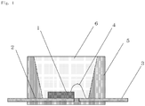
- FIG. 1 shows a cross-sectional drawing of a surface mounted type LED, which is one example of the optical semiconductor device of the present invention.
- an optical semiconductor element 1 is die-bonded to a lead frame 2, and the optical semiconductor element 1 and a lead frame 3 are wire-bonded by a bonding wire 4.
- a light reflection material 5 is formed on the periphery of this optical semiconductor element 1, and the optical semiconductor element 1 inside the light reflection material 5 is sealed by a cured product 6 of the curable silicone composition described above.
- An example of a method for producing the surface-mounted LED illustrated in FIG. 1 is a method of die-bonding the optical semiconductor element 1 to the lead frame 2, wire-bonding the optical semiconductor element 1 and the lead frame 3 with a bonding wire 4 made of gold, molding the curable silicone composition by transfer molding or compression molding, and then forming the light reflection material 5 on the periphery of the optical semiconductor element 1.
- Another example is a method of first forming the light reflection material 5 and then resin-sealing the optical semiconductor element 1 on the inside of the light reflection material 5 with the curable silicone composition described above.
- the curable silicone composition and optical semiconductor device of the present invention will be described in detail hereinafter using Practical Examples and Comparative Examples. Furthermore, the hardness of the cured product of the curable silicone composition, the storage stability of the curable silicone composition, and the color change of the cured product were measured as follows.
- the curable silicone composition was press-molded at 150°C for 1 hour at 5 MPa pressure to produce a sheet-like cured product.
- the hardness of the sheet-like cured product was measured by type A durometer as specified in JIS K 6253.
- a composition was prepared without adding a hydrosilylation reaction catalyst, and after storing for 100 hours in a 50°C oven, a curable silicone composition was prepared by adding a hydrosilylation reaction catalyst. After this thermal aging, the type A durometer hardness of the cured product obtained by heating the curable silicone composition at 150°C for 1 hour was measured. If the hardness after the thermal aging was lower than the hardness of the cured product obtained by curing the curable silicone composition before thermal aging, it was considered a "curing defect.” Furthermore, the appearance of the curable silicone composition after storage for 100 hours was observed macroscopically.
- the curable silicone composition was press-molded at 150°C for 1 hour at 5 MPa pressure to produce a sheet-like cured product.
- the sheet-like cured product was heated in nitrogen air flow at 200°C for 250 hours.
- the b value of the cured product in the CIE Lab standard colorimetric system according to JIS Z 8730 was measured using a colorimeter, and the b value after aging subtracted from the b value before aging was taken as the change in b value.
- optical semiconductor device illustrated in FIG. 1 was produced by heating at 150°C for 1 hour using the curable silicone composition. Sulfur resistance of this optical semiconductor device was measured as follows by measuring radiant flux.
- the initial radiant flux of the optical semiconductor device was measured by a total radiant flux measurement apparatus using integrating spheres. Then, the optical semiconductor device was put into an autoclave with sodium sulfide hexahydrate, heated to 50°C, and left to stand for 100 hours. After that, radiant flux of the optical semiconductor device was measured by a total radiant flux measurement apparatus using integrating spheres.
- component (A) The following components were used as component (A).
- the viscosity was the value at 25°C and was measured using a type B viscometer in accordance with JIS K7117-1.
- component (B) The following components were used as component (B).
- the viscosity was the value at 25°C and was measured using a type B viscometer in accordance with JIS K7117-1.
- component (C) The following components were used as component (C).
- the curable silicone composition of the present invention has excellent storage stability, and when cured, forms a cured product that undergoes minimal yellowing due to thermal aging and sufficiently suppresses discoloration of silver electrodes and silver plating of substrates due to sulfur-containing gas in the air.
- it is advantageous as a sealing agent, coating agent, or adhesive agent of optical semiconductor elements or a protective agent of silver electrodes of liquid crystal terminals and silver plating of substrates in optical semiconductor devices.
Applications Claiming Priority (3)
| Application Number | Priority Date | Filing Date | Title |
|---|---|---|---|
| JP2012268740 | 2012-12-07 | ||
| JP2013088755 | 2013-04-19 | ||
| PCT/JP2013/082906 WO2014088115A1 (ja) | 2012-12-07 | 2013-12-03 | 硬化性シリコーン組成物および光半導体装置 |
Publications (3)
| Publication Number | Publication Date |
|---|---|
| EP2930213A1 EP2930213A1 (en) | 2015-10-14 |
| EP2930213A4 EP2930213A4 (en) | 2016-08-03 |
| EP2930213B1 true EP2930213B1 (en) | 2021-08-25 |
Family
ID=50883526
Family Applications (1)
| Application Number | Title | Priority Date | Filing Date |
|---|---|---|---|
| EP13860333.7A Active EP2930213B1 (en) | 2012-12-07 | 2013-12-03 | Curable silicone composition and optical semiconductor device |
Country Status (7)
| Country | Link |
|---|---|
| US (1) | US20150299543A1 (ko) |
| EP (1) | EP2930213B1 (ko) |
| JP (1) | JP6223358B2 (ko) |
| KR (1) | KR101911690B1 (ko) |
| CN (1) | CN104837930B (ko) |
| TW (1) | TWI628234B (ko) |
| WO (1) | WO2014088115A1 (ko) |
Families Citing this family (17)
| Publication number | Priority date | Publication date | Assignee | Title |
|---|---|---|---|---|
| EP2984142B8 (en) * | 2013-04-10 | 2018-12-26 | Swimc Llc | Sour gas resistant coating |
| WO2015194159A1 (ja) * | 2014-06-20 | 2015-12-23 | 東レ・ダウコーニング株式会社 | オルガノポリシロキサンおよびその製造方法 |
| EP3229491A4 (en) * | 2014-12-01 | 2017-12-13 | Fujifilm Corporation | Composition for acoustic wave probe, silicone resin for acoustic wave probe using same, acoustic wave probe, ultrasonic probe, acoustic wave measurement device, ultrasonic diagnostic device, photoacoustic wave measurement device, and ultrasonic endoscope |
| CN105802238B (zh) * | 2014-12-31 | 2019-06-25 | 埃肯有机硅(上海)有限公司 | 可固化的聚硅氧烷组合物 |
| WO2016208640A1 (ja) * | 2015-06-24 | 2016-12-29 | 住友大阪セメント株式会社 | 硬化性シリコーン樹脂組成物、シリコーン樹脂複合体、光半導体発光装置、照明器具及び液晶画像装置 |
| WO2017002746A1 (ja) * | 2015-06-30 | 2017-01-05 | 富士フイルム株式会社 | 音響波プローブ用組成物、これを用いた音響波プローブ用シリコーン樹脂、音響波プローブおよび超音波プローブならびに音響波測定装置、超音波診断装置、光音響波測定装置および超音波内視鏡 |
| JP6347237B2 (ja) * | 2015-08-21 | 2018-06-27 | 信越化学工業株式会社 | 付加硬化型オルガノポリシロキサン組成物及び半導体装置 |
| US10513629B2 (en) * | 2015-10-26 | 2019-12-24 | Dow (Shanghai) Holding Co., Ltd. | Silicone release coating composition and article having cured release coating |
| JP2017088776A (ja) * | 2015-11-13 | 2017-05-25 | 信越化学工業株式会社 | 付加硬化型シリコーン樹脂組成物、該組成物の製造方法、及び光学半導体装置 |
| JPWO2017119363A1 (ja) * | 2016-01-08 | 2018-11-01 | 株式会社ダイセル | 硬化性シリコーン樹脂組成物及びその硬化物、並びに光半導体装置 |
| GB201603107D0 (en) * | 2016-02-23 | 2016-04-06 | Dow Corning | Low temperature cure silicone elastomer |
| CN105862017B (zh) * | 2016-04-20 | 2018-06-08 | 南昌大学 | 一种led银支架防银变色剂及制备和成膜方法 |
| EP3500629B1 (en) * | 2016-08-19 | 2024-01-31 | Dow Toray Co., Ltd. | Room temperature curable organopolysiloxane composition for protecting electric/electronic parts |
| JP6537763B1 (ja) * | 2017-10-04 | 2019-07-03 | 株式会社アドマテックス | シリコーン被覆フィラー及びその製造方法並びに樹脂組成物 |
| EP3868836A4 (en) * | 2018-10-18 | 2022-06-08 | Dow Toray Co., Ltd. | CURABLE SILICONE COMPOSITION AND CURED PRODUCT THEREOF, LAYER PRODUCT AND METHOD OF MANUFACTURE THEREOF, AND OPTICAL DEVICE OR DISPLAY |
| EP4065641A4 (en) * | 2019-11-25 | 2023-08-02 | Dow Silicones Corporation | FLAME RETARDANT POLYSILOXA COMPOSITION |
| CN112812741B (zh) * | 2021-01-27 | 2023-04-28 | 湖南柯盛新材料有限公司 | 一种双组份不可逆变色密封硅胶及其制备方法 |
Family Cites Families (15)
| Publication number | Priority date | Publication date | Assignee | Title |
|---|---|---|---|---|
| JPS5214654A (en) * | 1975-07-24 | 1977-02-03 | Shin Etsu Chem Co Ltd | An organopolysiloxane composition |
| JPS5558253A (en) * | 1978-10-25 | 1980-04-30 | Toshiba Silicone Co Ltd | Organopolysiloxane composition |
| JP3828612B2 (ja) * | 1996-05-24 | 2006-10-04 | 東レ・ダウコーニング株式会社 | 液状シリコーンゴム組成物およびその製造方法 |
| JP4833416B2 (ja) * | 2001-01-17 | 2011-12-07 | 株式会社カネカ | 硬化性組成物、製造方法、成形方法、および硬化物 |
| JP4676671B2 (ja) * | 2002-11-21 | 2011-04-27 | 東レ・ダウコーニング株式会社 | 熱伝導性シリコーンエラストマー組成物 |
| JP2006056986A (ja) * | 2004-08-19 | 2006-03-02 | Shin Etsu Chem Co Ltd | 二液硬化型シリコーン組成物 |
| JP2008150505A (ja) * | 2006-12-18 | 2008-07-03 | Momentive Performance Materials Japan Kk | シリコーンゴム組成物及び定着部材 |
| JP5053714B2 (ja) * | 2007-05-30 | 2012-10-17 | 株式会社カネカ | 付加型硬化性シリコーン組成物 |
| JP6014299B2 (ja) * | 2008-09-01 | 2016-10-25 | 東レ・ダウコーニング株式会社 | 熱伝導性シリコーン組成物及び半導体装置 |
| JP2010202731A (ja) * | 2009-03-02 | 2010-09-16 | Shin-Etsu Chemical Co Ltd | 紫外線遮蔽性シリコーンコーティング組成物及び被覆物品 |
| TWI406254B (zh) * | 2009-11-26 | 2013-08-21 | Chunghwa Picture Tubes Ltd | 可調變充放電時間之液晶顯示裝置及相關驅動方法 |
| JP4788837B2 (ja) | 2010-01-26 | 2011-10-05 | 横浜ゴム株式会社 | シリコーン樹脂組成物およびその使用方法、シリコーン樹脂、シリコーン樹脂含有構造体、ならびに光半導体素子封止体 |
| JP5534837B2 (ja) * | 2010-01-28 | 2014-07-02 | 東レ・ダウコーニング株式会社 | 熱伝導性シリコーンゴム組成物 |
| KR101296082B1 (ko) | 2010-11-17 | 2013-08-19 | 요코하마 고무 가부시키가이샤 | 실리콘 수지 조성물, 이것을 이용하는, 실리콘 수지 함유 구조체, 광반도체 소자 봉지체, 실리콘 수지 조성물의 사용 방법 |
| JP6569036B2 (ja) * | 2013-10-17 | 2019-09-04 | ダウ・東レ株式会社 | 硬化性シリコーン組成物および光半導体装置 |
-
2013
- 2013-12-03 US US14/650,034 patent/US20150299543A1/en not_active Abandoned
- 2013-12-03 JP JP2014551167A patent/JP6223358B2/ja active Active
- 2013-12-03 EP EP13860333.7A patent/EP2930213B1/en active Active
- 2013-12-03 KR KR1020157017751A patent/KR101911690B1/ko active IP Right Grant
- 2013-12-03 WO PCT/JP2013/082906 patent/WO2014088115A1/ja active Application Filing
- 2013-12-03 CN CN201380063965.9A patent/CN104837930B/zh active Active
- 2013-12-06 TW TW102144946A patent/TWI628234B/zh active
Also Published As
| Publication number | Publication date |
|---|---|
| EP2930213A1 (en) | 2015-10-14 |
| CN104837930B (zh) | 2020-10-16 |
| KR101911690B1 (ko) | 2018-10-25 |
| WO2014088115A1 (ja) | 2014-06-12 |
| JP6223358B2 (ja) | 2017-11-01 |
| JPWO2014088115A1 (ja) | 2017-01-05 |
| EP2930213A4 (en) | 2016-08-03 |
| KR20150092260A (ko) | 2015-08-12 |
| TW201428058A (zh) | 2014-07-16 |
| US20150299543A1 (en) | 2015-10-22 |
| TWI628234B (zh) | 2018-07-01 |
| CN104837930A (zh) | 2015-08-12 |
Similar Documents
| Publication | Publication Date | Title |
|---|---|---|
| EP2930213B1 (en) | Curable silicone composition and optical semiconductor device | |
| EP3039079B1 (en) | Curable silicone composition, cured product thereof, and optical semiconductor device | |
| EP3103843B1 (en) | Curable silicone composition, cured object thereof, and optical semiconductor device | |
| EP3153517A1 (en) | Organosiloxane, curable silicone composition, and semiconductor device | |
| EP2938655B1 (en) | Curable silicone composition, cured product thereof, and optical semiconductor device | |
| JP6586552B2 (ja) | 硬化性シリコーン組成物および光半導体装置 | |
| EP3103842B1 (en) | Curable silicone composition, cured object thereof, and optical semiconductor device | |
| WO2014104390A2 (en) | Curable silicone composition, cured product thereof, and optical semiconductor device | |
| EP3153516A1 (en) | Organic silicon compound, curable silicone composition, and semiconductor device | |
| EP2956508B1 (en) | Curable silicone composition, cured product thereof, and optical semiconductor device | |
| EP3153544A1 (en) | Adhesion promoter, curable silicone composition, and semiconductor device | |
| US11787943B2 (en) | Curable silicone composition and optical semiconductor device |
Legal Events
| Date | Code | Title | Description |
|---|---|---|---|
| PUAI | Public reference made under article 153(3) epc to a published international application that has entered the european phase |
Free format text: ORIGINAL CODE: 0009012 |
|
| STAA | Information on the status of an ep patent application or granted ep patent |
Free format text: STATUS: REQUEST FOR EXAMINATION WAS MADE |
|
| 17P | Request for examination filed |
Effective date: 20150609 |
|
| AK | Designated contracting states |
Kind code of ref document: A1 Designated state(s): AL AT BE BG CH CY CZ DE DK EE ES FI FR GB GR HR HU IE IS IT LI LT LU LV MC MK MT NL NO PL PT RO RS SE SI SK SM TR |
|
| AX | Request for extension of the european patent |
Extension state: BA ME |
|
| DAX | Request for extension of the european patent (deleted) | ||
| RA4 | Supplementary search report drawn up and despatched (corrected) |
Effective date: 20160701 |
|
| RIC1 | Information provided on ipc code assigned before grant |
Ipc: H01L 33/56 20100101ALI20160627BHEP Ipc: C08K 3/26 20060101ALI20160627BHEP Ipc: H01L 23/31 20060101ALI20160627BHEP Ipc: H01L 23/29 20060101ALI20160627BHEP Ipc: C08K 9/02 20060101ALI20160627BHEP Ipc: C08K 5/3472 20060101ALI20160627BHEP Ipc: C08K 9/06 20060101ALI20160627BHEP Ipc: H01L 23/28 20060101ALI20160627BHEP Ipc: C08L 83/04 20060101AFI20160627BHEP |
|
| RAP1 | Party data changed (applicant data changed or rights of an application transferred) |
Owner name: DUPONT TORAY SPECIALTY MATERIALS KABUSHIKI KAISHA |
|
| GRAP | Despatch of communication of intention to grant a patent |
Free format text: ORIGINAL CODE: EPIDOSNIGR1 |
|
| STAA | Information on the status of an ep patent application or granted ep patent |
Free format text: STATUS: GRANT OF PATENT IS INTENDED |
|
| INTG | Intention to grant announced |
Effective date: 20210617 |
|
| GRAS | Grant fee paid |
Free format text: ORIGINAL CODE: EPIDOSNIGR3 |
|
| GRAA | (expected) grant |
Free format text: ORIGINAL CODE: 0009210 |
|
| STAA | Information on the status of an ep patent application or granted ep patent |
Free format text: STATUS: THE PATENT HAS BEEN GRANTED |
|
| AK | Designated contracting states |
Kind code of ref document: B1 Designated state(s): AL AT BE BG CH CY CZ DE DK EE ES FI FR GB GR HR HU IE IS IT LI LT LU LV MC MK MT NL NO PL PT RO RS SE SI SK SM TR |
|
| REG | Reference to a national code |
Ref country code: GB Ref legal event code: FG4D |
|
| REG | Reference to a national code |
Ref country code: CH Ref legal event code: EP |
|
| REG | Reference to a national code |
Ref country code: IE Ref legal event code: FG4D Ref country code: AT Ref legal event code: REF Ref document number: 1423774 Country of ref document: AT Kind code of ref document: T Effective date: 20210915 |
|
| REG | Reference to a national code |
Ref country code: DE Ref legal event code: R096 Ref document number: 602013079000 Country of ref document: DE |
|
| REG | Reference to a national code |
Ref country code: LT Ref legal event code: MG9D |
|
| REG | Reference to a national code |
Ref country code: NL Ref legal event code: MP Effective date: 20210825 |
|
| REG | Reference to a national code |
Ref country code: AT Ref legal event code: MK05 Ref document number: 1423774 Country of ref document: AT Kind code of ref document: T Effective date: 20210825 |
|
| PG25 | Lapsed in a contracting state [announced via postgrant information from national office to epo] |
Ref country code: HR Free format text: LAPSE BECAUSE OF FAILURE TO SUBMIT A TRANSLATION OF THE DESCRIPTION OR TO PAY THE FEE WITHIN THE PRESCRIBED TIME-LIMIT Effective date: 20210825 Ref country code: SE Free format text: LAPSE BECAUSE OF FAILURE TO SUBMIT A TRANSLATION OF THE DESCRIPTION OR TO PAY THE FEE WITHIN THE PRESCRIBED TIME-LIMIT Effective date: 20210825 Ref country code: RS Free format text: LAPSE BECAUSE OF FAILURE TO SUBMIT A TRANSLATION OF THE DESCRIPTION OR TO PAY THE FEE WITHIN THE PRESCRIBED TIME-LIMIT Effective date: 20210825 Ref country code: BG Free format text: LAPSE BECAUSE OF FAILURE TO SUBMIT A TRANSLATION OF THE DESCRIPTION OR TO PAY THE FEE WITHIN THE PRESCRIBED TIME-LIMIT Effective date: 20211125 Ref country code: AT Free format text: LAPSE BECAUSE OF FAILURE TO SUBMIT A TRANSLATION OF THE DESCRIPTION OR TO PAY THE FEE WITHIN THE PRESCRIBED TIME-LIMIT Effective date: 20210825 Ref country code: LT Free format text: LAPSE BECAUSE OF FAILURE TO SUBMIT A TRANSLATION OF THE DESCRIPTION OR TO PAY THE FEE WITHIN THE PRESCRIBED TIME-LIMIT Effective date: 20210825 Ref country code: NO Free format text: LAPSE BECAUSE OF FAILURE TO SUBMIT A TRANSLATION OF THE DESCRIPTION OR TO PAY THE FEE WITHIN THE PRESCRIBED TIME-LIMIT Effective date: 20211125 Ref country code: PT Free format text: LAPSE BECAUSE OF FAILURE TO SUBMIT A TRANSLATION OF THE DESCRIPTION OR TO PAY THE FEE WITHIN THE PRESCRIBED TIME-LIMIT Effective date: 20211227 Ref country code: FI Free format text: LAPSE BECAUSE OF FAILURE TO SUBMIT A TRANSLATION OF THE DESCRIPTION OR TO PAY THE FEE WITHIN THE PRESCRIBED TIME-LIMIT Effective date: 20210825 Ref country code: ES Free format text: LAPSE BECAUSE OF FAILURE TO SUBMIT A TRANSLATION OF THE DESCRIPTION OR TO PAY THE FEE WITHIN THE PRESCRIBED TIME-LIMIT Effective date: 20210825 |
|
| PG25 | Lapsed in a contracting state [announced via postgrant information from national office to epo] |
Ref country code: PL Free format text: LAPSE BECAUSE OF FAILURE TO SUBMIT A TRANSLATION OF THE DESCRIPTION OR TO PAY THE FEE WITHIN THE PRESCRIBED TIME-LIMIT Effective date: 20210825 Ref country code: LV Free format text: LAPSE BECAUSE OF FAILURE TO SUBMIT A TRANSLATION OF THE DESCRIPTION OR TO PAY THE FEE WITHIN THE PRESCRIBED TIME-LIMIT Effective date: 20210825 Ref country code: GR Free format text: LAPSE BECAUSE OF FAILURE TO SUBMIT A TRANSLATION OF THE DESCRIPTION OR TO PAY THE FEE WITHIN THE PRESCRIBED TIME-LIMIT Effective date: 20211126 |
|
| PG25 | Lapsed in a contracting state [announced via postgrant information from national office to epo] |
Ref country code: NL Free format text: LAPSE BECAUSE OF FAILURE TO SUBMIT A TRANSLATION OF THE DESCRIPTION OR TO PAY THE FEE WITHIN THE PRESCRIBED TIME-LIMIT Effective date: 20210825 |
|
| PG25 | Lapsed in a contracting state [announced via postgrant information from national office to epo] |
Ref country code: DK Free format text: LAPSE BECAUSE OF FAILURE TO SUBMIT A TRANSLATION OF THE DESCRIPTION OR TO PAY THE FEE WITHIN THE PRESCRIBED TIME-LIMIT Effective date: 20210825 |
|
| REG | Reference to a national code |
Ref country code: DE Ref legal event code: R097 Ref document number: 602013079000 Country of ref document: DE |
|
| PG25 | Lapsed in a contracting state [announced via postgrant information from national office to epo] |
Ref country code: SM Free format text: LAPSE BECAUSE OF FAILURE TO SUBMIT A TRANSLATION OF THE DESCRIPTION OR TO PAY THE FEE WITHIN THE PRESCRIBED TIME-LIMIT Effective date: 20210825 Ref country code: SK Free format text: LAPSE BECAUSE OF FAILURE TO SUBMIT A TRANSLATION OF THE DESCRIPTION OR TO PAY THE FEE WITHIN THE PRESCRIBED TIME-LIMIT Effective date: 20210825 Ref country code: RO Free format text: LAPSE BECAUSE OF FAILURE TO SUBMIT A TRANSLATION OF THE DESCRIPTION OR TO PAY THE FEE WITHIN THE PRESCRIBED TIME-LIMIT Effective date: 20210825 Ref country code: EE Free format text: LAPSE BECAUSE OF FAILURE TO SUBMIT A TRANSLATION OF THE DESCRIPTION OR TO PAY THE FEE WITHIN THE PRESCRIBED TIME-LIMIT Effective date: 20210825 Ref country code: CZ Free format text: LAPSE BECAUSE OF FAILURE TO SUBMIT A TRANSLATION OF THE DESCRIPTION OR TO PAY THE FEE WITHIN THE PRESCRIBED TIME-LIMIT Effective date: 20210825 Ref country code: AL Free format text: LAPSE BECAUSE OF FAILURE TO SUBMIT A TRANSLATION OF THE DESCRIPTION OR TO PAY THE FEE WITHIN THE PRESCRIBED TIME-LIMIT Effective date: 20210825 |
|
| PLBE | No opposition filed within time limit |
Free format text: ORIGINAL CODE: 0009261 |
|
| STAA | Information on the status of an ep patent application or granted ep patent |
Free format text: STATUS: NO OPPOSITION FILED WITHIN TIME LIMIT |
|
| PG25 | Lapsed in a contracting state [announced via postgrant information from national office to epo] |
Ref country code: MC Free format text: LAPSE BECAUSE OF FAILURE TO SUBMIT A TRANSLATION OF THE DESCRIPTION OR TO PAY THE FEE WITHIN THE PRESCRIBED TIME-LIMIT Effective date: 20210825 Ref country code: IT Free format text: LAPSE BECAUSE OF FAILURE TO SUBMIT A TRANSLATION OF THE DESCRIPTION OR TO PAY THE FEE WITHIN THE PRESCRIBED TIME-LIMIT Effective date: 20210825 |
|
| REG | Reference to a national code |
Ref country code: CH Ref legal event code: PL |
|
| 26N | No opposition filed |
Effective date: 20220527 |
|
| GBPC | Gb: european patent ceased through non-payment of renewal fee |
Effective date: 20211203 |
|
| PG25 | Lapsed in a contracting state [announced via postgrant information from national office to epo] |
Ref country code: SI Free format text: LAPSE BECAUSE OF FAILURE TO SUBMIT A TRANSLATION OF THE DESCRIPTION OR TO PAY THE FEE WITHIN THE PRESCRIBED TIME-LIMIT Effective date: 20210825 |
|
| REG | Reference to a national code |
Ref country code: BE Ref legal event code: MM Effective date: 20211231 |
|
| PG25 | Lapsed in a contracting state [announced via postgrant information from national office to epo] |
Ref country code: LU Free format text: LAPSE BECAUSE OF NON-PAYMENT OF DUE FEES Effective date: 20211203 Ref country code: IE Free format text: LAPSE BECAUSE OF NON-PAYMENT OF DUE FEES Effective date: 20211203 Ref country code: GB Free format text: LAPSE BECAUSE OF NON-PAYMENT OF DUE FEES Effective date: 20211203 |
|
| PG25 | Lapsed in a contracting state [announced via postgrant information from national office to epo] |
Ref country code: FR Free format text: LAPSE BECAUSE OF NON-PAYMENT OF DUE FEES Effective date: 20211231 Ref country code: BE Free format text: LAPSE BECAUSE OF NON-PAYMENT OF DUE FEES Effective date: 20211231 |
|
| PG25 | Lapsed in a contracting state [announced via postgrant information from national office to epo] |
Ref country code: LI Free format text: LAPSE BECAUSE OF NON-PAYMENT OF DUE FEES Effective date: 20211231 Ref country code: CH Free format text: LAPSE BECAUSE OF NON-PAYMENT OF DUE FEES Effective date: 20211231 |
|
| PG25 | Lapsed in a contracting state [announced via postgrant information from national office to epo] |
Ref country code: HU Free format text: LAPSE BECAUSE OF FAILURE TO SUBMIT A TRANSLATION OF THE DESCRIPTION OR TO PAY THE FEE WITHIN THE PRESCRIBED TIME-LIMIT; INVALID AB INITIO Effective date: 20131203 |
|
| PG25 | Lapsed in a contracting state [announced via postgrant information from national office to epo] |
Ref country code: CY Free format text: LAPSE BECAUSE OF FAILURE TO SUBMIT A TRANSLATION OF THE DESCRIPTION OR TO PAY THE FEE WITHIN THE PRESCRIBED TIME-LIMIT Effective date: 20210825 |
|
| P01 | Opt-out of the competence of the unified patent court (upc) registered |
Effective date: 20230530 |
|
| PGFP | Annual fee paid to national office [announced via postgrant information from national office to epo] |
Ref country code: DE Payment date: 20231031 Year of fee payment: 11 |
|
| PG25 | Lapsed in a contracting state [announced via postgrant information from national office to epo] |
Ref country code: MK Free format text: LAPSE BECAUSE OF FAILURE TO SUBMIT A TRANSLATION OF THE DESCRIPTION OR TO PAY THE FEE WITHIN THE PRESCRIBED TIME-LIMIT Effective date: 20210825 |