EP2924743A1 - Light emitting device package - Google Patents
Light emitting device package Download PDFInfo
- Publication number
- EP2924743A1 EP2924743A1 EP15165853.1A EP15165853A EP2924743A1 EP 2924743 A1 EP2924743 A1 EP 2924743A1 EP 15165853 A EP15165853 A EP 15165853A EP 2924743 A1 EP2924743 A1 EP 2924743A1
- Authority
- EP
- European Patent Office
- Prior art keywords
- light emitting
- emitting device
- substrate
- device package
- mount
- Prior art date
- Legal status (The legal status is an assumption and is not a legal conclusion. Google has not performed a legal analysis and makes no representation as to the accuracy of the status listed.)
- Granted
Links
Images








Classifications
-
- H—ELECTRICITY
- H10—SEMICONDUCTOR DEVICES; ELECTRIC SOLID-STATE DEVICES NOT OTHERWISE PROVIDED FOR
- H10H—INORGANIC LIGHT-EMITTING SEMICONDUCTOR DEVICES HAVING POTENTIAL BARRIERS
- H10H20/00—Individual inorganic light-emitting semiconductor devices having potential barriers, e.g. light-emitting diodes [LED]
- H10H20/80—Constructional details
- H10H20/85—Packages
- H10H20/8506—Containers
-
- H—ELECTRICITY
- H10—SEMICONDUCTOR DEVICES; ELECTRIC SOLID-STATE DEVICES NOT OTHERWISE PROVIDED FOR
- H10W—GENERIC PACKAGES, INTERCONNECTIONS, CONNECTORS OR OTHER CONSTRUCTIONAL DETAILS OF DEVICES COVERED BY CLASS H10
- H10W90/00—Package configurations
-
- H—ELECTRICITY
- H10—SEMICONDUCTOR DEVICES; ELECTRIC SOLID-STATE DEVICES NOT OTHERWISE PROVIDED FOR
- H10H—INORGANIC LIGHT-EMITTING SEMICONDUCTOR DEVICES HAVING POTENTIAL BARRIERS
- H10H20/00—Individual inorganic light-emitting semiconductor devices having potential barriers, e.g. light-emitting diodes [LED]
- H10H20/80—Constructional details
- H10H20/85—Packages
- H10H20/855—Optical field-shaping means, e.g. lenses
- H10H20/856—Reflecting means
-
- H—ELECTRICITY
- H10—SEMICONDUCTOR DEVICES; ELECTRIC SOLID-STATE DEVICES NOT OTHERWISE PROVIDED FOR
- H10H—INORGANIC LIGHT-EMITTING SEMICONDUCTOR DEVICES HAVING POTENTIAL BARRIERS
- H10H20/00—Individual inorganic light-emitting semiconductor devices having potential barriers, e.g. light-emitting diodes [LED]
- H10H20/80—Constructional details
- H10H20/85—Packages
- H10H20/857—Interconnections, e.g. lead-frames, bond wires or solder balls
-
- H—ELECTRICITY
- H10—SEMICONDUCTOR DEVICES; ELECTRIC SOLID-STATE DEVICES NOT OTHERWISE PROVIDED FOR
- H10W—GENERIC PACKAGES, INTERCONNECTIONS, CONNECTORS OR OTHER CONSTRUCTIONAL DETAILS OF DEVICES COVERED BY CLASS H10
- H10W72/00—Interconnections or connectors in packages
- H10W72/851—Dispositions of multiple connectors or interconnections
- H10W72/874—On different surfaces
- H10W72/884—Die-attach connectors and bond wires
-
- H—ELECTRICITY
- H10—SEMICONDUCTOR DEVICES; ELECTRIC SOLID-STATE DEVICES NOT OTHERWISE PROVIDED FOR
- H10W—GENERIC PACKAGES, INTERCONNECTIONS, CONNECTORS OR OTHER CONSTRUCTIONAL DETAILS OF DEVICES COVERED BY CLASS H10
- H10W90/00—Package configurations
- H10W90/701—Package configurations characterised by the relative positions of pads or connectors relative to package parts
- H10W90/721—Package configurations characterised by the relative positions of pads or connectors relative to package parts of bump connectors
- H10W90/722—Package configurations characterised by the relative positions of pads or connectors relative to package parts of bump connectors between stacked chips
-
- H—ELECTRICITY
- H10—SEMICONDUCTOR DEVICES; ELECTRIC SOLID-STATE DEVICES NOT OTHERWISE PROVIDED FOR
- H10W—GENERIC PACKAGES, INTERCONNECTIONS, CONNECTORS OR OTHER CONSTRUCTIONAL DETAILS OF DEVICES COVERED BY CLASS H10
- H10W90/00—Package configurations
- H10W90/701—Package configurations characterised by the relative positions of pads or connectors relative to package parts
- H10W90/751—Package configurations characterised by the relative positions of pads or connectors relative to package parts of bond wires
- H10W90/756—Package configurations characterised by the relative positions of pads or connectors relative to package parts of bond wires between a chip and a stacked lead frame, conducting package substrate or heat sink
Definitions
- the present invention relates to a sub-mount for mounting a light emitting device and a light emitting device package, and more particularly, to a sub-mount for mounting a light emitting device which enables emission of light having a uniform intensity of illumination from the light emitting device, and a light emitting device package which is capable of having uniform brightness, using the sub-mount.
- GaN-based LED market has rapidly grown. Also, techniques associated with GaN-based electro-optic devices have rapidly developed since the GaN-based LEDs became commercially available in 1994.
- Such an LED is packaged together with other elements.
- An example of an LED package is illustrated in FIGs. 1 and 2 .
- the illustrated LED package includes a silicon sub-mount 2, on which an LED 1 is mounted, an aluminum slug 3, a printed circuit board (PCB) 4, and an aluminum heat sink 5.
- a silicon sub-mount 2 on which an LED 1 is mounted
- an aluminum slug 3 on which an LED 1 is mounted
- a printed circuit board (PCB) 4 on which an LED 1 is mounted
- an aluminum heat sink 5 on which an LED 1 is mounted
- PCB printed circuit board
- the silicon sub-mount 2 has metal lines formed on a flat silicon surface, for electrical connection with the LED 1.
- the LED 1 is bonded to the sub-mount 2 using a flip chip bonding process.
- the sub-mount 2 is bonded to a mirror surface of the aluminum slug 3 using an adhesive.
- the LED package having the above-mentioned structure, heat generated during operation of the LED is transferred to the aluminum heat sink 5 via the package body 6 and PCB 4.
- the package body 6 and PCB 4 are made of a plastic material that exhibits low heat transfer rate, the heat discharge is degraded, and thus, the optical characteristics of the LED are also degraded.
- a method comprises: forming through holes in a substrate at a region where a light emitting device is to be mounted, forming electrodes at opposite major surfaces of the substrate such that the electrodes are connected by the through holes, and separating each electrode into portions of different polarities.
- the method may further include forming an insulating layer on the substrate including the mount.
- the method may further include forming a diffusion barrier layer between the step of forming the adhesion layer and the step of forming the electrode metal layer.
- the diffusion barrier layer is made of at least one of Pt and Ni.
- the seed metal may be made of at least one of Au, Cu, and Al.
- the reflection layer may be made of Al or Ag.
- the separation of the seed metal and electrodes may be achieved using at least one of a plating and etching method or a lift-off method.
- a light emitting device package comprises: a package body having a mount for mounting a light emitting device, and through holes; electrodes formed on the package body; and a reflective layer arranged on an upper one of the electrodes of the package body, the reflective layer having a recess to which the light emitting device is mounted.
- the package body may comprise one of Si, Al, AlN, AlOx, photo sensitive glass (PSG), Al2O3, BeO, and PCB substrates.
- An insulating layer may be coated over the package body.
- Each electrode may comprise an adhesion layer coupled to the seed metal, and made of at least one of Ti, Cr, and Ta, and an electrode metal layer arranged on the adhesion layer, and made of at least one of Au, Cu, and Al.
- the seed metal may be made of at least one of Au, Cu, and Al.
- the light emitting device package may further comprise a lateral reflector arranged over the mount, and adapted to enable light emitted from the light emitting device to be laterally discharged.
- the lateral reflector may comprise a body having an opened side, and a groove communicating with the mount, and a reflective surface inclinedly formed at the groove.
- GaN gallium nitride
- Al2O3 sapphire
- a procedure for forming a mount 11, for example, a recess-shaped or groove shaped mount, on which a light emitting device will be mounted, and through holes 12 and 13 will be described with reference to FIGs. 3 to 6 .
- the substrate 10 may include a silicon substrate, or substrates made of other materials, namely, aluminum, aluminum nitride (AlN), aluminum oxide (AlOx), photo sensitive glass (PSG), Al2O3, and BeO.
- the substrate 10 may be a PCB substrate.
- Mask layers 20 made of, for example, a photoresist material, are then formed over opposite major surfaces of the prepared substrate 10.
- a substrate on which the mask layers 20 have previously been formed, may be prepared as the substrate 10.
- the mask layers 20 are then patterned to form mask patterns required for bulk-etching of a region where a light emitting device will be mounted, namely, a region where the recess-shaped mount 11 will be formed, and regions where the through holes 12 and 13 will be formed.
- the recess-shaped mount 11 for mounting the light emitting device and through holes 12 and 13 are formed by bulk-etching (bulk-micromachining) the substrate 10, using the mask patterns of the mask layers 20, as shown in FIG. 5 .
- a wet etching process, a dry etching process, or a laser drilling process may be used.
- a representative of the dry etching process may be a dip reactive ion etching process.
- the mount 11 and through holes 12 and 13 were formed at the substrate 10, using an isotropic wet etching solution such as KOH, tetramethyl ammonium hydroxide (THAH), or ethylene diamine pyrocatechol (EDP), under the condition in which a single-crystal silicon substrate having a [100] orientation is used for the substrate 10.
- an isotropic wet etching solution such as KOH, tetramethyl ammonium hydroxide (THAH), or ethylene diamine pyrocatechol (EDP)
- the mount 11 When the mount 11 is formed in accordance with the above-described method, it finally has an inclination of, ideally, 54.74°. Practically, the inclination of the mount 11 may be within a range of 50 to 60°.
- the width and depth of the mount 11 depend on the size or thickness of the light emitting device to be mounted. The width and depth of the mount 11 is determined such that light emitted laterally from the light emitting device is most effectively used.
- a region 21 where the light emitting device will be mounted and regions 22 where the through holes 12 and 13 will be formed are first patterned using masks. Thereafter, the regions 21 and 22 are simultaneously wet-etched to form the mount 11 and through holes 12 and 13.
- the mount 11 and through holes 12 and 13 may be formed using a silicon bulk micromachining process.
- the mask layers 20 are provided.
- the mask layers 20 should be made of a material capable of exhibiting a mask function for a prolonged period of time in an etching process.
- a silicon nitride film or a silicon oxide film is mainly used.
- the through holes 12 and 13 function to electrically connect front electrodes formed at the side of the mount 11 and rear electrodes formed at the opposite side of the mount 11.
- the through holes 12 and 13 are formed independently of each other such that the through hole 12 connects the positive electrodes, whereas the through hole 13 connects the negative electrodes.
- an insulating layer 30 is formed over the overall surface of the substrate 10 including the mount 11 and through holes 12 and 13, for electrical insulation of the substrate 10, as shown in FIG. 7 .
- a silicon nitride film may be deposited for the insulating layer 30, using an insulating layer formation method other than the above-described method, for example, a low pressure chemical vapor deposition (LPCVD) method or a plasma enhanced chemical vapor deposition (PECVD) method.
- LPCVD low pressure chemical vapor deposition
- PECVD plasma enhanced chemical vapor deposition
- the insulating layer 30 may be dispensed with in the case in which the substrate 10 is made of an insulating material such as an aluminum nitride (AlN) or an aluminum oxide (AlOx).
- AlN aluminum nitride
- AlOx aluminum oxide
- electrodes 50 including front electrodes 50a and rear electrodes 50b are formed on the substrate 10, which has a three-dimensional structure including the mount 11 for mounting a light emitting device, and the through holes 12 and 13, in accordance with a patterning process.
- the following three methods may be used.
- the first method is a method using electroplating.
- a seed metal 40 is first deposited on both major surfaces, namely, front and rear surfaces, of the substrate 10 which has a three-dimensional structure formed with the insulating layer 30 after the formation of the mount 11 and through holes 12 and 13, as shown in FIG. 8 .
- the seed metal 40 may be deposited on the surfaces of the through holes 12 and 13.
- the electrodes 50 which include the front and rear electrodes 50a and 50b, are formed on the seed metal 40 in accordance with an electroplating method or an electroless-plating method.
- the electrode formation may be achieved by patterning the photoresist before the formation of the electrodes 50, forming the electrodes 50 in accordance with a plating method, removing the photoresist, and etching the seed metal 40, to separate the positive and negative electrodes from each other.
- etching may also be carried out for the boundaries of the unit packages along singulation or dicing regions 52. In this case, it is possible to achieve an easy dicing process, or to prevent electric leakage after the dicing of the unit packages.
- the second method is a method using lift-off.
- a photoresist 21 is first coated over the front and rear surfaces of the substrate 10, as shown in FIG. 9 .
- Light exposure and development are then carried out, to separate the substrate 10 into portions respectively corresponding to positive and negative electrodes, and to separate the substrate 10 into portions respectively corresponding to unit packages.
- An electrode metal for the formation of the electrodes 50 is then deposited on the first and rear surfaces of the substrate 10 including the through holes in accordance with a sputtering method or an E-beam evaporation method. Thus, the structure as shown in FIG. 9 is obtained.
- an additional metal layer may be formed on the electrodes 50 in accordance with electroplating or electroless-plating.
- the third method is a combination of lift-off and electroplating.
- the front electrodes 50a or rear electrodes 50b are formed on the associated front or rear surface of the substrate 10 in accordance with the above-described lift-off method.
- electrodes are then formed on the surface of the substrate 10 opposite to the electrodes formed using the lift-off method. Thereafter, the front electrodes 50a and rear electrodes 50b are electrically connected via the through holes.
- the metal of the electrodes 50 should exhibit superior electrical characteristics, and a superior adhesion force to the insulating layer.
- a superior adhesion force to the insulating layer generally, titanium (Ti), chromium (Cr), or tantalum (Ta) exhibiting a superior adhesion force to a silicon oxide film, which is mainly used as an insulating layer, may be used.
- Gold Au
- Cu copper
- Al aluminum
- the electrode metal is exposed to a high temperature condition in a subsequent procedure, in particular, a process for coupling module elements.
- Ti or Cr which is the material of the adhesion layer
- a diffusion barrier layer made of, for example, platinum (Pt) or nickel (Ni), may be interposed between the adhesion layer of Ti or Cr and the Au layer.
- the electrodes 50 may have a structure of Ti/Pt/Au, Cr/Ni/Au, or Cr/Cu/Ni/Au.
- the electrode metal layer of the electrodes 50 is formed using the electroplating method, it is preferable to form the seed metal 40. Similarly to the electrode metal layer of the electrode 50, the seed metal 40 should exhibit superior electrical characteristics, and a superior adhesion force to the insulating layer 30.
- a reflective layer 60 is formed on the bottom and inclined surfaces of the mount 11, in order to achieve an enhancement in the efficiency of light emitted from the light emitting device mounted on the mount 11.
- the reflective layer 60 may be made of a material exhibiting a superior reflectivity, such as aluminum (Al) or silver (Ag).
- the formation of the reflective layer 60 may be achieved by coating a photoresist over the overall surface of the substrate 10, patterning the coated photoresist in accordance with light exposure and development such that the bottom or inclined surface of the mount 11, on which the light emitting device will be mounted, is exposed, depositing a reflective material in accordance with a sputtering method or an E-beam evaporation method, and lifting off the patterned photoresist.
- the reflective layer 60 may be formed by depositing a reflective material over the overall surface of the substrate 10, and then etching unnecessary portions of the deposited reflective material.
- the reflection layer 60 should be formed to prevent it from being connected to or overlapped with both the positive and negative ones of the electrodes 50a and 50b, in order to prevent electrical short-circuit. In order to enable the reflection layer 60 to adhere to the electrode metal, it is preferred that the reflective layer 60 is not present on the reflection layer 60 at regions where solderings or Au studs 71 ( FIG. 13 ) will be formed.
- a light emitting device 70 such as an LED is bonded to the front electrodes 50a, in accordance with a bonding method using solderings or Au studs, such that the light emitting device 70 is electrically connected to the front electrodes 50a, as shown in FIG. 13 .
- the light emitting device 70 is mounted on the mount 11.
- An encapsulating material 80 which is made of phosphor, silicon gel, or epoxy resin having superior optical transmittance, is then filled in the mount 11.
- the encapsulating material 80 is applied over the substrate 10 such that it encloses the light emitting device 70.
- the transfer molding process is carried out under the condition in which a tape is attached to a lower surface of the substrate 10, in order to prevent the encapsulating material 80 from being attached to the electrodes 50, and thus, contaminating the electrodes 50.
- the solderings for bonding of the light emitting device 70 may be performed, using gold-tin (AuSn), lead-tin (PbSn), or indium (In), in accordance with an E-beam evaporation method.
- AuSn gold-tin
- PbSn lead-tin
- In indium
Landscapes
- Led Device Packages (AREA)
- Led Devices (AREA)
Abstract
Description
- The present invention relates to a sub-mount for mounting a light emitting device and a light emitting device package, and more particularly, to a sub-mount for mounting a light emitting device which enables emission of light having a uniform intensity of illumination from the light emitting device, and a light emitting device package which is capable of having uniform brightness, using the sub-mount.
- Light emitting diodes (LEDs) are well known as semiconductor light emitting devices that convert current to light. A red LED using GaAsP compound semiconductor has been commercially available since 1962, and together with a GaP:N-based green LED, has been a light source in electronic apparatuses, such as image displays.
- A wavelength of light emitted from such an LED depends on a semiconductor material used to fabricate the LED. This is because the wavelength of the emitted light depends on a band gap of the semiconductor material representing energy difference between valence-band electrons and conduction-band electrons.
- Gallium nitride (GaN) compound semiconductor has been highlighted in the field of high-power electronic devices because it exhibits a high thermal stability and a wide band gap of 0.8 to 6.2 eV. One of the reasons why GaN compound semiconductor has been highlighted is that it is possible to fabricate a semiconductor layer capable of emitting green, blue, or white light, using GaN in combination with other elements, for example, indium (In), aluminum (Al), etc.
- That is, it is possible to adjust the wavelength of light to be emitted, using GaN in combination with other appropriate elements. For example, it is possible to fabricate a blue LED useful for optical recording or a white LED to replace a glow lamp.
- By virtue of the recent success of growth of InGaN thin film, it has been possible to fabricate high-luminescent green LEDs. In contrast, initially-developed green LEDs were fabricated using GaP. Because GaP is an indirect transition material, there is degradation in efficiency. Thus, the green LEDs fabricated using this material could not practically produce a pure green light.
- By virtue of the above-mentioned advantages and other advantages of GaN-based LEDs, the GaN-based LED market has rapidly grown. Also, techniques associated with GaN-based electro-optic devices have rapidly developed since the GaN-based LEDs became commercially available in 1994.
- GaN-based LEDs have been developed to exhibit light emission efficiency superior over that of glow lamps. Currently, the efficiency of GaN-based LEDs is substantially equal to that of fluorescent lamps. Thus, it is expected that the GaN-based LED market will grow significantly.
- Such an LED is packaged together with other elements. An example of an LED package is illustrated in
FIGs. 1 and 2 . - The illustrated LED package includes a
silicon sub-mount 2, on which anLED 1 is mounted, analuminum slug 3, a printed circuit board (PCB) 4, and analuminum heat sink 5. - The
silicon sub-mount 2 has metal lines formed on a flat silicon surface, for electrical connection with theLED 1. - The
LED 1 is bonded to thesub-mount 2 using a flip chip bonding process. Thesub-mount 2 is bonded to a mirror surface of thealuminum slug 3 using an adhesive. -
Leads 6a are fixedly mounted to apackage body 6. The leads are electrically connected to electrode metal portions of thesub-mount 2 viaconductive wires 7, respectively. - The
PCB 4 is bonded to thepackage body 6 using an adhesive, and includesmetal lines 4a to which theleads 6a are attached using a welding process. Thealuminum heat sink 5 is attached to thePCB 4, in order to allow heat from thePCB 4 to be outwardly discharged via thealuminum heat sink 5. - In the LED package having the above-mentioned structure, heat generated during operation of the LED is transferred to the
aluminum heat sink 5 via thepackage body 6 andPCB 4. However, because thepackage body 6 and PCB 4 are made of a plastic material that exhibits low heat transfer rate, the heat discharge is degraded, and thus, the optical characteristics of the LED are also degraded. - In particular, it is difficult to implement an illumination apparatus such as a backlight, using LCD packages having the above-mentioned structure, due to problems associated with size, light uniformity, and costs. Also, degradation in productivity and reliability may occur because precise wire bonding may be required.
- Accordingly, various embodiments of the present invention are directed to a sub-mount for mounting a light emitting device and a light emitting device package that substantially obviate one or more problems due to limitations and disadvantages of the related art.
- An object of the present invention is to provide a sub-mount for mounting a light emitting device that enables emission of light having a uniform intensity of illumination from the light emitting device, and a light emitting device package that is capable of having uniform brightness, using the sub-mount.
- Additional advantages, objects, and features of the invention will be set forth in part in the description which follows and in part will become apparent to those having ordinary skill in the art upon examination of the following or may be learned from practice of the invention. The objectives and other advantages of the invention may be realized and attained by the structure particularly pointed out in the written description and claims hereof as well as the appended drawings. The present invention is defined in
claim 1. - To achieve these objects and other advantages and in accordance with the purpose of the invention, as embodied and broadly described herein, a method comprises: forming through holes in a substrate at a region where a light emitting device is to be mounted, forming electrodes at opposite major surfaces of the substrate such that the electrodes are connected by the through holes, and separating each electrode into portions of different polarities.
- The method may further include forming an insulating layer on the substrate including the mount.
- The method may further include a reflective layer having openings for connecting the light emitting device to the electrodes, respectively.
- The method may further include coupling the electrodes to the light emitting device via the openings, coating an encapsulating material over the mount, to which the light emitting device is mounted, and bonding a lens to an upper surface of the encapsulating material.
- The formation of the mount and the formation of the through holes may be simultaneously achieved by simultaneously etching both the opposite major surfaces of the substrate.
- Preferably, the seed metal and electrodes are simultaneously separated into portions respectively corresponding to unit packages at the step of separating the electrodes. The step of forming electrodes may comprise forming an adhesion layer on the seed metal, and forming an electrode metal layer on the adhesion layer.
- The adhesion layer may be made of at least one of Ti, Cr, and Ta. The electrode metal layer may be made of at least one of Au, Cu, and Al.
- The method may further include forming a diffusion barrier layer between the step of forming the adhesion layer and the step of forming the electrode metal layer. Preferably, the diffusion barrier layer is made of at least one of Pt and Ni.
- The seed metal may be made of at least one of Au, Cu, and Al. The reflection layer may be made of Al or Ag.
- The separation of the seed metal and electrodes may be achieved using at least one of a plating and etching method or a lift-off method.
- The formation of the mount or through hole may be achieved using one of wet etching, dry etching, and laser drilling. In particular, the dry etching is preferably achieved using a deep RIE method.
- In another aspect of the present invention, a sub-mount structure for mounting light emitting devices comprises: a substrate; a plurality of mounts formed on an upper surface of the substrate, and adapted to mount the light emitting devices; through holes respectively formed at opposite sides of each mount; electrodes, each extending to a lower surface of the substrate via an inner surface of an associated one of the mounts and an associated one of the through holes; and a reflective layer arranged on one of the electrodes arranged on the mount, the reflective layer having a recess to which the light emitting device is mounted.
- In another aspect of the present invention, a light emitting device package comprises: a package body having a mount for mounting a light emitting device, and through holes; electrodes formed on the package body; and a reflective layer arranged on an upper one of the electrodes of the package body, the reflective layer having a recess to which the light emitting device is mounted.
- The package body may comprise one of Si, Al, AlN, AlOx, photo sensitive glass (PSG), Al2O3, BeO, and PCB substrates. An insulating layer may be coated over the package body.
- Each electrode may comprise an adhesion layer coupled to the seed metal, and made of at least one of Ti, Cr, and Ta, and an electrode metal layer arranged on the adhesion layer, and made of at least one of Au, Cu, and Al.
- The light emitting device package may further comprise a diffusion barrier layer formed between the adhesion layer and the electrode metal layer, and made of at least one of Pt and Ni.
- The seed metal may be made of at least one of Au, Cu, and Al.
- The light emitting device package may further comprise a lateral reflector arranged over the mount, and adapted to enable light emitted from the light emitting device to be laterally discharged.
- The lateral reflector may comprise a body having an opened side, and a groove communicating with the mount, and a reflective surface inclinedly formed at the groove.
- It is to be understood that both the foregoing general description and the following detailed description of the present invention are exemplary and explanatory and are not intended to limit the scope of the claims.
- The accompanying drawings, which are included to provide a further understanding of the invention and are incorporated in and constitute a part of this application, illustrate embodiment(s) of the invention and together with the description serve to explain the principle of the invention. In the drawings:
-
FIG. 1 is a perspective view illustrating an example of a conventional light emitting device package; -
FIG. 2 is a sectional view illustrating the conventional light emitting device package; -
FIGs. 3 to 14 are sectional views illustrating a first embodiment of the present invention, in which: -
FIG. 3 is a sectional view illustrating formation of a mask layer; -
FIG. 4 is a sectional view illustrating patterning of the mask layer; -
FIG. 5 is a sectional view illustrating formation of a mount and through holes; -
FIG. 6 is a sectional view illustrating a state in which the mask layer has been removed; -
FIG. 7 is a sectional view illustrating formation of an insulating layer; -
FIG. 8 is a sectional view illustrating formation of a seed metal; -
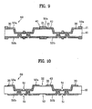
FIG. 9 is a sectional view illustrating an example of electrode formation; -
FIG. 10 is a sectional view illustrating formation of electrodes; -
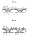
FIG. 11 is a sectional view illustrating a state in which each electrode has been separated into electrode portions; -
FIG. 12 is a sectional view illustrating formation of a reflective layer; -
FIG. 13 is a sectional view illustrating formation using encapsulating material; -
FIG. 14 is a sectional view illustrating formation of a lens; -
FIG. 15 is a sectional view illustrating a second embodiment of the present invention; -
FIG. 16 is a sectional view illustrating a third embodiment of the present invention; -
FIG. 17 is a sectional view illustrating a fourth embodiment of the present invention; -
FIG. 18 is a sectional view illustrating a fifth embodiment of the present invention; -
FIG. 19 is a sectional view illustrating a sixth embodiment of the present invention; -
FIG. 20 is a sectional view illustrating a seventh embodiment of the present invention; -
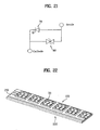
FIG. 21 is a circuit diagram illustrating the seventh embodiment of the present invention; -
FIG. 22 is a perspective view illustrating an example of an illumination apparatus to which embodiments of the present invention can be applied; -
FIG. 23 is a perspective view illustrating an example of a light emitting device package according to an embodiment of the present invention; -
FIG. 24 is a perspective view illustrating another example of the light emitting device package according to an embodiment of the present invention; -
FIG. 25 is a perspective view illustrating an example of a lateral reflector according to an eighth embodiment of the present invention; -
FIG. 26 is a perspective view illustrating a state in which the lateral reflector according to an embodiment of the present invention is mounted to a light emitting device package; and -
FIG. 27 is a perspective view illustrating an example of an illumination apparatus using the lateral reflector according to an embodiment of the present invention. - The present invention now will be described more fully hereinafter with reference to the accompanying figures, in which embodiments of the invention are shown. This invention may, however, be embodied in many alternate forms and should not be construed as limited to the embodiments set forth herein. Accordingly, while the invention is susceptible to various modifications and alternative forms, specific embodiments thereof are shown by way of example in the drawings and will herein be described in detail.
- Like numbers refer to like elements throughout the description of the figures. In the drawings, the thickness of layers and regions are exaggerated for clarity.
- It will be understood that when an element such as a layer, region or substrate is referred to as being "on" another element, it can be directly on the other element or intervening elements may also be present. It will also be understood that if part of an element, such as a surface, is referred to as "inner," it is farther to the outside of the device than other parts of the element.
- It will be understood that these terms are intended to encompass different orientations of the device in addition to the orientation depicted in the figures. Finally, the term "directly" means that there are no intervening elements. As used herein, the term "and/or" includes any and all combinations of one or more of the associated listed items.
- It will be understood that, although the terms first, second, etc. may be used herein to describe various elements, components, regions, layers and/or sections, these elements, components, regions, layers and/or sections should not be limited by these terms.
- Preferred embodiments of the present invention will be described, for example, with reference to a gallium nitride (GaN)-based light emitting diode (LED) formed on a nonconductive substrate such as a sapphire (Al2O3)-based substrate. However, the present invention is not limited to such a structure.
- The embodiments of the present invention may employ other kinds of substrates including a conductive substrate. Therefore, the embodiments of the present invention may include AlGaInP LEDs on a GaP substrate, GaN LEDs on an SiC substrate, SiC diodes on a sapphire substrate, and/or any combination of nitride-based LEDs on GaN, SiC, AlN, ZnO and/or other substrates. Further, in the present invention, use of an active layer region is not limited to LED regions. In addition, other forms of the active layer region may be employed in compliance with some embodiments of the present invention.
- First, a procedure for forming a
mount 11, for example, a recess-shaped or groove shaped mount, on which a light emitting device will be mounted, and throughholes FIGs. 3 to 6 . - In this procedure, a substrate is first prepared, as shown in
FIG. 3 . Thesubstrate 10 may include a silicon substrate, or substrates made of other materials, namely, aluminum, aluminum nitride (AlN), aluminum oxide (AlOx), photo sensitive glass (PSG), Al2O3, and BeO. Thesubstrate 10 may be a PCB substrate. - Mask layers 20 made of, for example, a photoresist material, are then formed over opposite major surfaces of the
prepared substrate 10. Alternatively, a substrate, on which the mask layers 20 have previously been formed, may be prepared as thesubstrate 10. As shown inFIG. 4 , the mask layers 20 are then patterned to form mask patterns required for bulk-etching of a region where a light emitting device will be mounted, namely, a region where the recess-shapedmount 11 will be formed, and regions where the throughholes mount 11 for mounting the light emitting device and throughholes substrate 10, using the mask patterns of the mask layers 20, as shown inFIG. 5 . - For the bulk-etching process, which is adapted to form the recess-shaped
mount 11 and throughholes - A representative of the dry etching process may be a dip reactive ion etching process.
- In this embodiment, the
mount 11 and throughholes substrate 10, using an isotropic wet etching solution such as KOH, tetramethyl ammonium hydroxide (THAH), or ethylene diamine pyrocatechol (EDP), under the condition in which a single-crystal silicon substrate having a [100] orientation is used for thesubstrate 10. - When the
mount 11 is formed in accordance with the above-described method, it finally has an inclination of, ideally, 54.74°. Practically, the inclination of themount 11 may be within a range of 50 to 60°. - The width and depth of the
mount 11 depend on the size or thickness of the light emitting device to be mounted. The width and depth of themount 11 is determined such that light emitted laterally from the light emitting device is most effectively used. - For the wet etching process for forming the
mount 11 and throughholes - In a first method, a
region 21 where the light emitting device will be mounted andregions 22 where the throughholes regions mount 11 and throughholes - The
mount 11 and throughholes - In a second method, a mask patterning process is first carried out for the
region 21 where the light emitting device will be mounted or theregions 22 where the throughholes region 21 orregions 22. During this etching process, a mask patterning process is carried out for the remainingregion 21 orregions 22. After this mask patterning process, the remainingregion 21 orregions 22 are etched. In this case, it is possible to adjust the ratio between the depth of themount 11 and the depth of the throughholes - In order to define a portion of the
substrate 10 to be etched and a portion of thesubstrate 10 to be protected from an etching process, the mask layers 20 are provided. The mask layers 20 should be made of a material capable of exhibiting a mask function for a prolonged period of time in an etching process. For the mask layers 20, a silicon nitride film or a silicon oxide film is mainly used. - The through holes 12 and 13 function to electrically connect front electrodes formed at the side of the
mount 11 and rear electrodes formed at the opposite side of themount 11. In order to separate the electrodes into two polarities, namely, a positive polarity and a negative polarity, it is preferred that the throughholes hole 12 connects the positive electrodes, whereas the throughhole 13 connects the negative electrodes. - Next, an insulating
layer 30 is formed over the overall surface of thesubstrate 10 including themount 11 and throughholes substrate 10, as shown inFIG. 7 . - For the formation of the insulating
layer 30, themask layer 20, which was used for the formation of themount 11 and throughholes FIG. 6 . A silicon oxide film exhibiting excellent insulation characteristics is formed over the overall surface of thesubstrate 10 in accordance with a thermal oxidation method. - A silicon nitride film may be deposited for the insulating
layer 30, using an insulating layer formation method other than the above-described method, for example, a low pressure chemical vapor deposition (LPCVD) method or a plasma enhanced chemical vapor deposition (PECVD) method. - The insulating
layer 30 may be dispensed with in the case in which thesubstrate 10 is made of an insulating material such as an aluminum nitride (AlN) or an aluminum oxide (AlOx). - Thereafter,
electrodes 50 includingfront electrodes 50a andrear electrodes 50b are formed on thesubstrate 10, which has a three-dimensional structure including themount 11 for mounting a light emitting device, and the throughholes - For the method for forming the
electrodes 50 using a patterning process, the following three methods may be used. - The first method is a method using electroplating.
- In this method, a
seed metal 40 is first deposited on both major surfaces, namely, front and rear surfaces, of thesubstrate 10 which has a three-dimensional structure formed with the insulatinglayer 30 after the formation of themount 11 and throughholes FIG. 8 . In this case, theseed metal 40 may be deposited on the surfaces of the throughholes - Thereafter, the
electrodes 50, which include the front andrear electrodes seed metal 40 in accordance with an electroplating method or an electroless-plating method. - Subsequently, photoresist coating, light exposure, and development are sequentially carried out, to etch the
electrodes 50 such that theelectrodes 50 are separated into positive and negative electrodes alongseparation grooves 51. A patterning process is then carried out to connect thefront electrodes 50a and therear electrodes 50b via the throughholes FIG. 10 is completely formed. - The electrode formation may be achieved by patterning the photoresist before the formation of the
electrodes 50, forming theelectrodes 50 in accordance with a plating method, removing the photoresist, and etching theseed metal 40, to separate the positive and negative electrodes from each other. - At this time, etching may also be carried out for the boundaries of the unit packages along singulation or dicing
regions 52. In this case, it is possible to achieve an easy dicing process, or to prevent electric leakage after the dicing of the unit packages. - The second method is a method using lift-off.
- In this method, a
photoresist 21 is first coated over the front and rear surfaces of thesubstrate 10, as shown inFIG. 9 . Light exposure and development are then carried out, to separate thesubstrate 10 into portions respectively corresponding to positive and negative electrodes, and to separate thesubstrate 10 into portions respectively corresponding to unit packages. - An electrode metal for the formation of the
electrodes 50 is then deposited on the first and rear surfaces of thesubstrate 10 including the through holes in accordance with a sputtering method or an E-beam evaporation method. Thus, the structure as shown inFIG. 9 is obtained. - The
photoresist 21 is then lifted off. In accordance with the lift-off of thephotoresist 21, the portions of theelectrodes 50 on thephotoresist 21 are removed. Thus, theelectrodes 50 are separated into positive and negative electrodes as shown inFIG. 11 . At this time, thesubstrate 10 is also separated into portions respectively corresponding to unit packages. - In order to increase the thickness of the
electrodes 50, an additional metal layer may be formed on theelectrodes 50 in accordance with electroplating or electroless-plating. - The third method is a combination of lift-off and electroplating.
- In this method, the
front electrodes 50a orrear electrodes 50b are formed on the associated front or rear surface of thesubstrate 10 in accordance with the above-described lift-off method. - In accordance with an electroplating or electroless-plating method, electrodes are then formed on the surface of the
substrate 10 opposite to the electrodes formed using the lift-off method. Thereafter, thefront electrodes 50a andrear electrodes 50b are electrically connected via the through holes. - In this case, the metal of the
electrodes 50 should exhibit superior electrical characteristics, and a superior adhesion force to the insulating layer. For an adhesion layer of the electrode metal, generally, titanium (Ti), chromium (Cr), or tantalum (Ta) exhibiting a superior adhesion force to a silicon oxide film, which is mainly used as an insulating layer, may be used. - Gold (Au), copper (Cu), or aluminum (Al) may be used which is a representative electrode metal exhibiting superior electrical characteristics while being easily depositable in a semiconductor process.
- The electrode metal is exposed to a high temperature condition in a subsequent procedure, in particular, a process for coupling module elements. For this reason, Ti or Cr, which is the material of the adhesion layer, may be diffused into Au, thereby degrading the electrical characteristics of Au. To this end, a diffusion barrier layer made of, for example, platinum (Pt) or nickel (Ni), may be interposed between the adhesion layer of Ti or Cr and the Au layer.
- Thus, the
electrodes 50 may have a structure of Ti/Pt/Au, Cr/Ni/Au, or Cr/Cu/Ni/Au. - Where the electrode metal layer of the
electrodes 50 is formed using the electroplating method, it is preferable to form theseed metal 40. Similarly to the electrode metal layer of theelectrode 50, theseed metal 40 should exhibit superior electrical characteristics, and a superior adhesion force to the insulatinglayer 30. - For an adhesion layer of the electrode metal, titanium (Ti), chromium (Cr), or tantalum (Ta) is used. For the seed metal, gold (Au), copper (Cu), or aluminum (Al) is used. Accordingly, a structure of Cu/Au, Cr/Cu, Ti/Au, or Ta/Ti/Cu may be formed. Thus, the
electrodes 50 may form a structure of Cr/Cu/Cu/Ni/Au, Cr/Au/Au, or Cr/Au/Cu/Ni/Au, together with theseed metal 40. - After the formation of the
electrode 50, areflective layer 60 is formed on the bottom and inclined surfaces of themount 11, in order to achieve an enhancement in the efficiency of light emitted from the light emitting device mounted on themount 11. - The
reflective layer 60 may be made of a material exhibiting a superior reflectivity, such as aluminum (Al) or silver (Ag). - The formation of the
reflective layer 60 may be achieved by coating a photoresist over the overall surface of thesubstrate 10, patterning the coated photoresist in accordance with light exposure and development such that the bottom or inclined surface of themount 11, on which the light emitting device will be mounted, is exposed, depositing a reflective material in accordance with a sputtering method or an E-beam evaporation method, and lifting off the patterned photoresist. - Alternatively, the
reflective layer 60 may be formed by depositing a reflective material over the overall surface of thesubstrate 10, and then etching unnecessary portions of the deposited reflective material. - The
reflection layer 60 should be formed to prevent it from being connected to or overlapped with both the positive and negative ones of theelectrodes reflection layer 60 to adhere to the electrode metal, it is preferred that thereflective layer 60 is not present on thereflection layer 60 at regions where solderings or Au studs 71 (FIG. 13 ) will be formed. - Next, a
light emitting device 70 such as an LED is bonded to thefront electrodes 50a, in accordance with a bonding method using solderings or Au studs, such that thelight emitting device 70 is electrically connected to thefront electrodes 50a, as shown inFIG. 13 . At this time, thelight emitting device 70 is mounted on themount 11. An encapsulatingmaterial 80, which is made of phosphor, silicon gel, or epoxy resin having superior optical transmittance, is then filled in themount 11. - That is, when a transfer molding process is carried out after the bonding of the
light emitting device 70 to thesubstrate 10, the encapsulatingmaterial 80 is applied over thesubstrate 10 such that it encloses thelight emitting device 70. - The transfer molding process is carried out under the condition in which a tape is attached to a lower surface of the
substrate 10, in order to prevent the encapsulatingmaterial 80 from being attached to theelectrodes 50, and thus, contaminating theelectrodes 50. - It is possible to vary the wavelength of light emitted from the
light emitting device 70 when the encapsulatingmaterial 80 is made of a molding composite resin in which phosphor powder is dispersed. - For example, where the light emitted from the
light emitting device 70 is blue light, and the phosphor powder is green and red phosphor powder, the blue light emitted from thelight emitting device 70 and incident to the green and red phosphor powder dispersed in the encapsulatingmaterial 80 is outwardly emitted after being wavelength-varied to green light and red right. In this case, the blue light emitted from thelight emitting device 70, but not incident to the green and red phosphor powder dispersed in the encapsulatingmaterial 80, is outwardly emitted as is. As a result, white light, which is a combination of the blue light, green light, and red light, is outwardly emitted. - Thus, light sources capable of emitting light of various wavelengths including a white light source can be implemented.
- Accordingly, it is preferred that the phosphor powder comprise one or two of blue phosphor powder, green phosphor powder, red phosphor powder, and yellow phosphor powder.
- The filling of the encapsulating
material 80 may be carried out after thesubstrate 10 is diced into portions respectively corresponding to unit packages, namely, sub-mount units. Alternatively, the filling of the encapsulatingmaterial 80 may be carried out before the dicing of thesubstrate 10. In this case, light emittingdevices 70 for respective unit packages are first bonded to thesubstrate 10. The encapsulatingmaterial 80 is then filled on thesubstrate 10. Thereafter, thesubstrate 10 is diced into portions respectively corresponding to unit packages, namely, sub-mount units. - The solderings for bonding of the
light emitting device 70 may be performed, using gold-tin (AuSn), lead-tin (PbSn), or indium (In), in accordance with an E-beam evaporation method. - If necessary, a lens sheet having a predetermined shape may then be bonded to or formed on the
substrate 10, to form alens 81 for controlling the distribution of light emitted from thelight emitting device 70, as shown inFIG. 14 . - In this case, an encapsulating
material 80 may be partially or completely applied on the surface of the lens sheet opposite to the surface formed with thelens 81, using silicon gel containing phosphor or epoxy resin having superior optical transmittance, in accordance with a screen printing method. Thus, it is possible to fabricate thelens 81 using a lens sheet having a lens structure at one surface and an encapsulating material containing phosphor at the other surface. - The lens sheet having the above-described structure may be subsequently bonded to the
substrate 10 carrying thelight emitting device 70, in accordance with a laminating process. The resultant package may then be diced into unit packages. - Hereinafter, various other embodiments of the present invention will be described with reference to the annexed drawings. Elements of each embodiment, not described, may be similar to those of the first embodiment.
-
FIG. 15 illustrates an embodiment in which alight emitting device 72 is bonded to thesubstrate 10 in accordance with a wire bondingprocess using wires 73, differently from the case ofFIG. 14 . - In particular, where a vertical
light emitting device 72 having electrodes at the top and bottom thereof is used, the lower electrode of thelight emitting device 72 is bonded to one of thefront electrodes 50a via awire 73, whereas the upper electrode of thelight emitting device 72 is bonded to the otherfront electrode 50a having a polarity opposite to that of the one-side front electrode 50a via awire 73. - The remaining fabrication processes and structures of this embodiment are similar to those of the first embodiment.
-
FIG. 16 illustrates a structure in which themount 11 or each throughhole light emitting device 70 has a vertical surface in accordance with a third embodiment of the present invention. - In accordance with this embodiment, the
mount 11 or each throughhole - The
mount 11 or each throughhole substrate 10. - When the through
holes front electrode 50a andrear electrode 50b to come into contact with each other via the throughholes - Referring to
FIG. 17 , a light emitting device package including one or more light emitting chips, for example, red, green, and blue light emitting chips, is illustrated. - In accordance with a fourth embodiment of the present invention, the
electrodes 50 andseed metal 40, andreflective layer 60, which correspond to one unit package, may be formed such that they are separated into portions respectively corresponding to regions where light emittingdevices devices substrate 10 at a region corresponding to one unit package. - When red, green, and blue light emitting devices are mounted to one unit package, it is possible to implement one white light emitting device package.
- In this case, at least one light emitting device emitting one of primary color lights, namely, red, green and blue lights, may be included in the unit package.
-
FIG. 18 illustrates an embodiment wherein a light emitting device package is formed, in which thesubstrate 10 is formed with only the throughholes light emitting device 70. - In this case, it is possible to simplify the fabrication process by virtue of no formation of the mount.
- In this case, it is also possible to reduce the thickness of the light emitting device package. When the
electrodes seed metal 40 may be dispensed with. - As shown in
FIG. 19 , it is possible to form the through holes along the side wall of the substrate without forming the through holes at the top portion of the substrate or at the mount. - That is, in accordance with a sixth embodiment of the present invention, through
holes 14 may be formed along a dicing region corresponding to the boundary of adjacent unit packages. In this case, a package having a three-dimensional structure is fabricated. - Since the through
holes 14 are formed along the dicing region, it is possible to more easily achieve the dicing of the fabricated package into unit packages. - In this case, the
electrodes 50 are electrically connected via the through holes 14. - In accordance with a seventh embodiment of the present invention, it is possible to embed
zener diodes 90 in thesubstrate 10 under the condition in which a silicon substrate is used for thesubstrate 10, as shown inFIG. 20 . - The embedding of the
zener diodes 90 may be achieved using one of the following methods. - The first method is to implant P-type dopant ions such as boron ions into an N-type substrate.
- The second method is to implant N-type dopant ions such as PoCl3 ions into a P-
type substrate 10. - For example, the first method is adapted to form a semiconductor PNP junction structure by doping boron ions into the
substrate 10 at a region where N and P-type electrodes come into contact with each other, such that the N and P-type electrodes are electrically connected. - In accordance with such a structure of the
zener diodes 90, current is bypassed by thezener diodes 90 when an overvoltage is applied to thelight emitting device 70 due to static electricity. Accordingly, it is possible to prevent thelight emitting device 70 from being damaged. - It is preferred that the silicon substrate used in association with the formation of the
zener diodes 90 have a resistance of 0.01 to 1.0 Ohm/cm. -
FIG. 21 is a circuit diagram of the light emitting device package in which thezener diodes 90 are embedded as described inFIG. 20 . - Referring to
FIG. 22 , a light emittingdevice package 100 is illustrated which may be fabricated in accordance with one of the above-described embodiments as illumination apparatuses for various purposes using light emitting devices. As shown inFIG. 22 , the light emittingdevice package 100, which is of a sub-mount type, is bonded to a system formed with anelectrode line 210 for supplying electric power to the light emitting device of thepackage 100. -
FIG. 22 illustrates the case in which a plurality of light emittingdevices 70 are mounted to onepackage 100. - For example, a combination of red, green and blue
light emitting devices 70 is incorporated in onepackage 100, to implement an illumination device emitting white light or various other lights. - The mounted state of one
light emitting device 70 to thesubstrate 10 may be as illustrated inFIG. 23 . - Referring to
FIG. 23 , an example of a package is illustrated wherein alight emitting device 70 is mounted to asubstrate 10 at a region where amount 11 is formed, and throughholes mount 11, respectively. - As shown in
FIG. 24 , at least one of the side walls of themount 11, for example, theside wall 11a, may be laterally opened, in order to enable lateral light emission. - In order to achieve an enhancement in the efficiency of lateral light emission in the light emitting device package having the above-described structure, a
lateral reflector 300 may be provided, as shown inFIG. 25 . - The
lateral reflector 300 is adapted to enable light emitted from thelight emitting device 70 to be laterally discharged. As shown inFIG. 25 , thelateral reflector 300 is formed with agroove 310 at oneside surface 301, and is opened at a portion of abottom surface 302, to communicate with themount 11. - An
inclined surface 320 is formed at one surface of thegroove 310, in order to enable the light emitted from thelight emitting device 70 to be efficiently laterally discharged. The inclination of theinclined surface 320 is preferably 45°. - A reflective surface may be formed on the inclined surface, using a mirror coating method or the like.
-
FIG. 26 is a perspective view illustrating a state in which thelateral reflector 300 ofFIG. 25 is mounted to the top of the light emitting device package. As shown inFIG. 26 , thelateral reflector 300 is mounted to thesubstrate 10 of the light emitting device package such that thegroove 310 of thelateral reflector 300 communicates with themount 11 of thesubstrate 10. - By virtue of the
lateral reflector 300, light emitted from thelight emitting device 70 mounted in the package is more effectively discharged from the associated side surface of the package. -
FIG. 27 illustrates a state in which a plurality of light emitting device packages havinglateral reflectors 300 are arranged in the form of a matrix in accordance with an embodiment of the present invention. - Thus, a package capable of laterally emitting light can be implemented by mounting
lateral reflectors 300 to thesubstrate 10 on which light emitting devices are mounted. - Features of the present disclosure are further defined in the following sections A to I:
- A. A light emitting device package comprising:
- a package body having a recess-shaped mount for mounting a light emitting diode (70), and through holes;
- seed metal layer formed on the package body;
- electrodes formed on the seed metal layer, the electrodes connected with the light emitting diode electrically, wherein the electrodes comprises an adhesion layer, an electrode metal, and a diffusion barrier layer that is between the adhesion layer and the electrode metal; and
- a reflective layer (60) arranged on the electrodes,
- wherein the seed metal is made of at least one of Au, Cu, and Al,
- wherein the adhesion layer is made of at least one of Ti, Cr, and Ta, and couples the electrode metal to the seed metal,
- wherein the electrode metal layer is made of at least one of Au, Cu, and Al, and
- wherein the diffusion barrier layer is made of at least one of Pt and Ni, and prevents a material in the adhesion layer from being diffused into the electrode metal.
- B. The light emitting device package according to section A, wherein the reflective layer is made of Al or Ag.
- C. The light emitting device package according to section A, wherein a plurality of the light emitting diode is mounted on the mount.
- D. The light emitting device package according to section C, wherein each of the light emitting diodes emits red, green, or blue light.
- E. The light emitting device package according to section A, further comprising:
- an insulating layer coated over the package body.
- F. The light emitting device package according to section A, further comprising:
- the light emitting diode coupled to the electrodes;
- an encapsulating material filled over the light emitting diode; and
- a lens attached to an upper surface of the encapsulating material.
- G. The light emitting device package according to section F, wherein the encapsulating material is made of at least one of silicone gel, phosphor, and epoxy resin.
- H. The light emitting device package according to section A, wherein the recess-shaped mount is formed by etching the package body.
- I. The light emitting device package according to section H, wherein the mount has inclined side walls.
Claims (15)
- A light emitting device package comprising;
a substrate having through holes;
a seed metal disposed inside the through and on an upper surface and a lower surface of the substrate; and
an electrode disposed inside the through hole and on the upper surface and a lower surface of the substrate, the electrode includes a diffusion barrier layer, an electrode metal layer and surface metal, the diffusion barrier layer prevents the electrode metal layer from being degraded in characteristics. - The light emitting device package according to claim 1, wherein the seed metal on the upper surface of the substrate are contact with the seed metal on the lower surface of the substrate by seed metal inside the through holes.
- The light emitting device package according to claim 1 or claim, 2, wherein the electrode on the upper surface of the substrate are contact with the electrode on the lower surface of the substrate by the electrode inside the through holes.
- The light emitting device package according any one of to claim 1 to 3, wherein the surface metal is a reflective layer having a recess.
- The light emitting device package according to claim 3, further comprising a light emitting device mounted on the recess.
- The light emitting device package according to any one of claim 1 to 5, wherein the surface metal is Au studs.
- The light emitting device package according to any one of claim 1 to 6, wherein the surface metal includes Au.
- The light emitting device package according to ant one of claim 1 to 7, wherein the substrate includes at least one of Si, AlN, AlOx, Al2O3, and BeO.
- The light emitting device package according to any one of claim 1 to 4 or 6 to 8, wherein the substrate includes at least one groove, and further comprising a light emitting device is disposed on the groove.
- The light emitting device package according to any one of claim 1 to 9, wherein the electrode is disposed on the seed metal disposed on the upper surface and the lower surface of the substrate.
- The light emitting device package according to any one of claim 1 to 10, wherein the diffusion barrier layer includes at least two metals.
- The light emitting device package according to any one of claim 11, wherein one of the metals is Ni.
- The light emitting device package according to any one of claim 5 or 9 to 12, further comprising a lens disposed above the light emitting device.
- The light emitting device package according to any one of claim 1 to 13, further comprising a zener diode disposed on the substrate.
- The light emitting device package according to any one of claims 1 to 14, wherein three or four light emitting devices are mounted on the substrate.
Applications Claiming Priority (2)
| Application Number | Priority Date | Filing Date | Title |
|---|---|---|---|
| KR1020060063873A KR100854328B1 (en) | 2006-07-07 | 2006-07-07 | Light emitting device package and its manufacturing method |
| EP06291846.1A EP1876653B1 (en) | 2006-07-07 | 2006-11-30 | Sub-mount for mounting light emitting diode and light emitting diode package |
Related Parent Applications (2)
| Application Number | Title | Priority Date | Filing Date |
|---|---|---|---|
| EP06291846.1A Division EP1876653B1 (en) | 2006-07-07 | 2006-11-30 | Sub-mount for mounting light emitting diode and light emitting diode package |
| EP06291846.1A Division-Into EP1876653B1 (en) | 2006-07-07 | 2006-11-30 | Sub-mount for mounting light emitting diode and light emitting diode package |
Publications (2)
| Publication Number | Publication Date |
|---|---|
| EP2924743A1 true EP2924743A1 (en) | 2015-09-30 |
| EP2924743B1 EP2924743B1 (en) | 2021-05-12 |
Family
ID=38519714
Family Applications (2)
| Application Number | Title | Priority Date | Filing Date |
|---|---|---|---|
| EP06291846.1A Active EP1876653B1 (en) | 2006-07-07 | 2006-11-30 | Sub-mount for mounting light emitting diode and light emitting diode package |
| EP15165853.1A Active EP2924743B1 (en) | 2006-07-07 | 2006-11-30 | Light emitting device package |
Family Applications Before (1)
| Application Number | Title | Priority Date | Filing Date |
|---|---|---|---|
| EP06291846.1A Active EP1876653B1 (en) | 2006-07-07 | 2006-11-30 | Sub-mount for mounting light emitting diode and light emitting diode package |
Country Status (6)
| Country | Link |
|---|---|
| US (1) | US7714341B2 (en) |
| EP (2) | EP1876653B1 (en) |
| JP (1) | JP5036287B2 (en) |
| KR (1) | KR100854328B1 (en) |
| CN (1) | CN100539218C (en) |
| DE (1) | DE202006021128U1 (en) |
Families Citing this family (177)
| Publication number | Priority date | Publication date | Assignee | Title |
|---|---|---|---|---|
| US4720124A (en) | 1985-08-02 | 1988-01-19 | Cameron Iron Works, Inc. | Telescoping joint |
| KR101059361B1 (en) * | 2003-01-16 | 2011-08-24 | 파나소닉 주식회사 | Lead frame and semiconductor light emitting device |
| JP2007201420A (en) * | 2005-12-27 | 2007-08-09 | Sharp Corp | Semiconductor light emitting device, semiconductor light emitting element, and method for manufacturing semiconductor light emitting device |
| TWI302758B (en) * | 2006-04-21 | 2008-11-01 | Silicon Base Dev Inc | Package base structure of photo diode and manufacturing method of the same |
| US8698184B2 (en) | 2011-01-21 | 2014-04-15 | Cree, Inc. | Light emitting diodes with low junction temperature and solid state backlight components including light emitting diodes with low junction temperature |
| US9443903B2 (en) * | 2006-06-30 | 2016-09-13 | Cree, Inc. | Low temperature high strength metal stack for die attachment |
| KR20080057881A (en) * | 2006-12-21 | 2008-06-25 | 엘지전자 주식회사 | Printed circuit board, light emitting device comprising same and manufacturing method thereof |
| KR100851183B1 (en) * | 2006-12-27 | 2008-08-08 | 엘지이노텍 주식회사 | Semiconductor light emitting device package |
| TWM318792U (en) * | 2007-01-23 | 2007-09-11 | Lighthouse Technology Co Ltd | Package structure |
| US7732234B2 (en) | 2007-02-15 | 2010-06-08 | Hymite A/S | Fabrication process for package with light emitting device on a sub-mount |
| JP5179766B2 (en) * | 2007-03-08 | 2013-04-10 | スタンレー電気株式会社 | Semiconductor light emitting device and manufacturing method thereof |
| KR100850666B1 (en) * | 2007-03-30 | 2008-08-07 | 서울반도체 주식회사 | LED package with metal PC |
| TW200843135A (en) * | 2007-04-23 | 2008-11-01 | Augux Co Ltd | Method of packaging light emitting diode with high heat-dissipating efficiency and the structure thereof |
| EP1988577B1 (en) * | 2007-04-30 | 2017-04-05 | Tridonic Jennersdorf GmbH | Light emitting diode module with silicon platform |
| US8436371B2 (en) * | 2007-05-24 | 2013-05-07 | Cree, Inc. | Microscale optoelectronic device packages |
| KR100877881B1 (en) | 2007-09-06 | 2009-01-08 | 엘지이노텍 주식회사 | Light emitting diode package and its manufacturing method |
| JP4809308B2 (en) * | 2007-09-21 | 2011-11-09 | 新光電気工業株式会社 | Substrate manufacturing method |
| TWI353657B (en) * | 2007-09-28 | 2011-12-01 | Ind Tech Res Inst | An island submount |
| KR100891810B1 (en) * | 2007-11-06 | 2009-04-07 | 삼성전기주식회사 | White light emitting device |
| US7985970B2 (en) | 2009-04-06 | 2011-07-26 | Cree, Inc. | High voltage low current surface-emitting LED |
| KR101491138B1 (en) * | 2007-12-12 | 2015-02-09 | 엘지이노텍 주식회사 | Multi-layer substrate and light-emitting diode module |
| KR100976497B1 (en) * | 2008-02-28 | 2010-08-18 | 엘지전자 주식회사 | Light emitting device package and its manufacturing method |
| KR100998009B1 (en) * | 2008-03-12 | 2010-12-03 | 삼성엘이디 주식회사 | Light emitting diode package and manufacturing method thereof |
| JP5185683B2 (en) * | 2008-04-24 | 2013-04-17 | パナソニック株式会社 | LED module manufacturing method and lighting apparatus manufacturing method |
| DE102008021402B4 (en) | 2008-04-29 | 2023-08-10 | OSRAM Opto Semiconductors Gesellschaft mit beschränkter Haftung | Surface mount light emitting diode module and method for manufacturing a surface mount light emitting diode module |
| DE102008021659A1 (en) * | 2008-04-30 | 2009-11-05 | Ledon Lighting Jennersdorf Gmbh | LED element with a thin film semiconductor device based on gallium nitride |
| KR101526567B1 (en) | 2008-05-07 | 2015-06-10 | 엘지이노텍 주식회사 | Lighting emitting diode package |
| KR100992778B1 (en) | 2008-05-23 | 2010-11-05 | 엘지이노텍 주식회사 | Light emitting device package and method for manufacturing the same |
| KR20100003320A (en) * | 2008-06-24 | 2010-01-08 | 엘지이노텍 주식회사 | Light emitting diode package |
| US8044427B2 (en) | 2008-06-24 | 2011-10-25 | Dicon Fiberoptics, Inc. | Light emitting diode submount with high thermal conductivity for high power operation |
| US20100001305A1 (en) * | 2008-07-07 | 2010-01-07 | Visera Technologies Company Limited | Semiconductor devices and fabrication methods thereof |
| KR101510474B1 (en) * | 2008-10-27 | 2015-04-08 | 엘지전자 주식회사 | Light emitting device package and manufacturing method thereof |
| TW201020643A (en) * | 2008-11-25 | 2010-06-01 | Chi Mei Lighting Tech Corp | Side view type light-emitting diode package structure, and manufacturing method and application thereof |
| KR101521260B1 (en) * | 2008-11-25 | 2015-05-18 | 삼성전자주식회사 | Light emitting diode package and manufacturing method thereof |
| TWI426206B (en) * | 2008-12-25 | 2014-02-11 | 友達光電股份有限公司 | Light-emitting diode device |
| KR101047801B1 (en) * | 2008-12-29 | 2011-07-07 | 엘지이노텍 주식회사 | Light emitting device package and manufacturing method thereof |
| US8598602B2 (en) * | 2009-01-12 | 2013-12-03 | Cree, Inc. | Light emitting device packages with improved heat transfer |
| US7923739B2 (en) * | 2009-06-05 | 2011-04-12 | Cree, Inc. | Solid state lighting device |
| USD648686S1 (en) | 2010-04-30 | 2011-11-15 | Cree, Inc. | Light emitting diode (LED) package |
| USD621799S1 (en) | 2009-01-12 | 2010-08-17 | Cree, Inc. | Light emitting diode |
| USD641719S1 (en) | 2009-06-05 | 2011-07-19 | Cree, Inc. | Light emitting diode |
| CN101800219B (en) * | 2009-02-09 | 2019-09-17 | 晶元光电股份有限公司 | light-emitting element |
| KR101565749B1 (en) | 2009-02-09 | 2015-11-13 | 삼성전자 주식회사 | Fabricating method of light emitting device |
| CN101800275B (en) * | 2009-02-11 | 2012-09-05 | 奇力光电科技股份有限公司 | Side-view light-emitting diode packaging structure and its manufacturing method and application |
| US8729591B2 (en) * | 2009-02-13 | 2014-05-20 | Tsmc Solid State Lighting Ltd. | Opto-electronic device package with a semiconductor-based sub-mount having SMD metal contacts |
| KR101077264B1 (en) * | 2009-02-17 | 2011-10-27 | (주)포인트엔지니어링 | Substrate for optical device, optical device package having the same and menufacturing method thereof |
| KR101114592B1 (en) | 2009-02-17 | 2012-03-09 | 엘지이노텍 주식회사 | Lighting emitting device and fabrication method thereof |
| KR101064026B1 (en) * | 2009-02-17 | 2011-09-08 | 엘지이노텍 주식회사 | Light emitting device package and manufacturing method thereof |
| CN101515621B (en) * | 2009-02-19 | 2011-03-30 | 旭丽电子(广州)有限公司 | Light-emitting diode chip, manufacturing method and packaging method |
| KR101020993B1 (en) * | 2009-03-10 | 2011-03-09 | 엘지이노텍 주식회사 | Light emitting device package and its manufacturing method |
| US20120049214A1 (en) * | 2009-04-06 | 2012-03-01 | Lowes Theodore D | Monolithic Multi-Junction Light Emitting Devices Including Multiple Groups of Light Emitting Diodes |
| US8476668B2 (en) * | 2009-04-06 | 2013-07-02 | Cree, Inc. | High voltage low current surface emitting LED |
| US9093293B2 (en) | 2009-04-06 | 2015-07-28 | Cree, Inc. | High voltage low current surface emitting light emitting diode |
| JP5343831B2 (en) | 2009-04-16 | 2013-11-13 | 日亜化学工業株式会社 | Light emitting device |
| CN101901794B (en) * | 2009-05-25 | 2012-08-15 | 光宏精密股份有限公司 | Plastic lead frame structure with reflective and conductive metal layer and method for making same |
| USD648687S1 (en) | 2009-06-05 | 2011-11-15 | Cree, Inc. | Light emitting device package |
| US8686445B1 (en) | 2009-06-05 | 2014-04-01 | Cree, Inc. | Solid state lighting devices and methods |
| US8860043B2 (en) * | 2009-06-05 | 2014-10-14 | Cree, Inc. | Light emitting device packages, systems and methods |
| KR100986544B1 (en) * | 2009-06-10 | 2010-10-07 | 엘지이노텍 주식회사 | Semiconductor light emitting device and fabrication method thereof |
| JP2011009519A (en) * | 2009-06-26 | 2011-01-13 | Hitachi Chem Co Ltd | Optical semiconductor device and method for manufacturing the optical semiconductor device |
| DE102009032486A1 (en) * | 2009-07-09 | 2011-01-13 | Osram Opto Semiconductors Gmbh | Optoelectronic component |
| US8530990B2 (en) * | 2009-07-20 | 2013-09-10 | Sunpower Corporation | Optoelectronic device with heat spreader unit |
| KR20110014867A (en) * | 2009-08-06 | 2011-02-14 | 삼성전기주식회사 | Power device package and manufacturing method thereof |
| US8933644B2 (en) | 2009-09-18 | 2015-01-13 | Soraa, Inc. | LED lamps with improved quality of light |
| US9293644B2 (en) | 2009-09-18 | 2016-03-22 | Soraa, Inc. | Power light emitting diode and method with uniform current density operation |
| US8258722B2 (en) * | 2009-09-24 | 2012-09-04 | Cree, Inc. | Lighting device with defined spectral power distribution |
| US8791492B2 (en) | 2009-10-01 | 2014-07-29 | Excelitas Canada, Inc. | Semiconductor laser chip package with encapsulated recess molded on substrate and method for forming same |
| US8431951B2 (en) * | 2009-10-01 | 2013-04-30 | Excelitas Canada, Inc. | Optoelectronic devices with laminate leadless carrier packaging in side-looker or top-looker device orientation |
| US9018074B2 (en) | 2009-10-01 | 2015-04-28 | Excelitas Canada, Inc. | Photonic semiconductor devices in LLC assembly with controlled molding boundary and method for forming same |
| KR101039930B1 (en) * | 2009-10-23 | 2011-06-09 | 엘지이노텍 주식회사 | Light emitting device package and manufacturing method thereof |
| JP5526712B2 (en) * | 2009-11-05 | 2014-06-18 | 豊田合成株式会社 | Semiconductor light emitting device |
| US7893445B2 (en) * | 2009-11-09 | 2011-02-22 | Cree, Inc. | Solid state emitter package including red and blue emitters |
| KR100962706B1 (en) * | 2009-11-27 | 2010-06-15 | 주식회사 테크엔 | Manufacture method of the large illuminations with power led |
| JP5505005B2 (en) * | 2009-12-22 | 2014-05-28 | 豊田合成株式会社 | Light emitting device |
| KR101072212B1 (en) * | 2010-01-05 | 2011-10-10 | 엘지이노텍 주식회사 | Light emitting device and method for fabricating the same |
| KR101134815B1 (en) * | 2010-01-15 | 2012-04-13 | 엘지이노텍 주식회사 | Display device and manufacturing method of the same |
| US9299664B2 (en) * | 2010-01-18 | 2016-03-29 | Semiconductor Components Industries, Llc | Method of forming an EM protected semiconductor die |
| KR101091304B1 (en) * | 2010-01-20 | 2011-12-07 | 엘지이노텍 주식회사 | Light emitting device package and its manufacturing method |
| US8905588B2 (en) | 2010-02-03 | 2014-12-09 | Sorra, Inc. | System and method for providing color light sources in proximity to predetermined wavelength conversion structures |
| US10147850B1 (en) | 2010-02-03 | 2018-12-04 | Soraa, Inc. | System and method for providing color light sources in proximity to predetermined wavelength conversion structures |
| US8558262B2 (en) * | 2010-02-12 | 2013-10-15 | Xintec Inc. | High-reflection submount for light-emitting diode package and fabrication method thereof |
| TWI393274B (en) * | 2010-02-26 | 2013-04-11 | 榮創能源科技股份有限公司 | Light emitting diode package and method for manufacturing same |
| CN102194809A (en) * | 2010-03-11 | 2011-09-21 | 许凯淳 | Large-area light-emitting diode module and packaging method thereof |
| KR101020974B1 (en) * | 2010-03-17 | 2011-03-09 | 엘지이노텍 주식회사 | Light emitting device, light emitting device manufacturing method and light emitting device package |
| KR101121151B1 (en) * | 2010-03-19 | 2012-03-20 | 주식회사 대원이노스트 | Led module and fabrication method of thereof |
| KR101028329B1 (en) * | 2010-04-28 | 2011-04-12 | 엘지이노텍 주식회사 | Light emitting device package and its manufacturing method |
| KR101653684B1 (en) * | 2010-05-28 | 2016-09-02 | 삼성전자 주식회사 | Light emitting device, Light emitting system comprising the same, and method of fabricating thereof |
| US8552458B2 (en) * | 2010-06-26 | 2013-10-08 | SemiLEDs Optoelectronics Co., Ltd. | Side by side light emitting diode (LED) having separate electrical and heat transfer paths |
| US8269244B2 (en) | 2010-06-28 | 2012-09-18 | Cree, Inc. | LED package with efficient, isolated thermal path |
| US8648359B2 (en) | 2010-06-28 | 2014-02-11 | Cree, Inc. | Light emitting devices and methods |
| DE102010026344A1 (en) * | 2010-07-07 | 2012-01-12 | Osram Opto Semiconductors Gmbh | led |
| USD643819S1 (en) | 2010-07-16 | 2011-08-23 | Cree, Inc. | Package for light emitting diode (LED) lighting |
| DE102010027679A1 (en) | 2010-07-20 | 2012-01-26 | Osram Opto Semiconductors Gmbh | Optoelectronic component |
| US8563849B2 (en) | 2010-08-03 | 2013-10-22 | Sunpower Corporation | Diode and heat spreader for solar module |
| CN102386306B (en) * | 2010-08-27 | 2016-04-13 | 比亚迪股份有限公司 | A kind of method for packing of LED chip and encapsulating structure |
| KR101124816B1 (en) * | 2010-09-24 | 2012-03-26 | 서울옵토디바이스주식회사 | Light emitting diode package and method of manufacturing thereof |
| KR101119950B1 (en) * | 2010-09-28 | 2012-03-16 | 경북대학교 산학협력단 | Light-emitting diode package having narrow emitting angle |
| US20120074432A1 (en) * | 2010-09-29 | 2012-03-29 | Amtran Technology Co., Ltd | Led package module and manufacturing method thereof |
| CN102447035B (en) * | 2010-10-06 | 2015-03-25 | 赛恩倍吉科技顾问(深圳)有限公司 | LED (light emitting diode) as well as mold and method for manufacturing LED |
| EP2447595B1 (en) * | 2010-10-27 | 2017-08-02 | LG Innotek Co., Ltd. | Light emitting module |
| KR20130143061A (en) | 2010-11-03 | 2013-12-30 | 쓰리엠 이노베이티브 프로퍼티즈 컴파니 | Flexible led device with wire bond free die |
| CN102479889A (en) * | 2010-11-30 | 2012-05-30 | 中芯国际集成电路制造(上海)有限公司 | Method of forming an optical platform |
| KR101677063B1 (en) * | 2010-12-09 | 2016-11-17 | (주)에이엘에스 | Lead Flame Substrate for LED Package and Method of Manufacturing of The Same |
| KR101677062B1 (en) * | 2010-12-09 | 2016-11-17 | (주)에이엘에스 | Lead Flame Substrate for LED Package and Method of Manufacturing of The Same |
| USD679842S1 (en) | 2011-01-03 | 2013-04-09 | Cree, Inc. | High brightness LED package |
| US8610140B2 (en) | 2010-12-15 | 2013-12-17 | Cree, Inc. | Light emitting diode (LED) packages, systems, devices and related methods |
| US11101408B2 (en) | 2011-02-07 | 2021-08-24 | Creeled, Inc. | Components and methods for light emitting diode (LED) lighting |
| TW201230417A (en) * | 2011-01-11 | 2012-07-16 | Lextar Electronics Corp | Leadframe, packaging cup incorporating the leadframe and light emitting diode lamp having the leadframe |
| US8236584B1 (en) | 2011-02-11 | 2012-08-07 | Tsmc Solid State Lighting Ltd. | Method of forming a light emitting diode emitter substrate with highly reflective metal bonding |
| KR101761834B1 (en) * | 2011-01-28 | 2017-07-27 | 서울바이오시스 주식회사 | Wafer level led package and method of fabricating the same |
| TW201251140A (en) | 2011-01-31 | 2012-12-16 | Cree Inc | High brightness light emitting diode (LED) packages, systems and methods with improved resin filling and high adhesion |
| US9716061B2 (en) | 2011-02-18 | 2017-07-25 | 3M Innovative Properties Company | Flexible light emitting semiconductor device |
| CN102694081B (en) * | 2011-03-21 | 2014-11-05 | 展晶科技(深圳)有限公司 | Method for manufacturing light emitting diode |
| WO2012128270A1 (en) * | 2011-03-24 | 2012-09-27 | 株式会社村田製作所 | Light-emitting-element base substrate, and led device |
| KR101181224B1 (en) * | 2011-03-29 | 2012-09-10 | 성균관대학교산학협력단 | Led package and fabricating method of the same |
| KR101863868B1 (en) * | 2011-04-08 | 2018-06-01 | 엘지이노텍 주식회사 | Light emitting device module and illumination system including the same |
| US8829557B2 (en) * | 2011-04-08 | 2014-09-09 | Lg Innotek Co., Ltd. | Light emitting device module and lighting system including the same |
| KR101785645B1 (en) * | 2011-05-30 | 2017-10-16 | 엘지이노텍 주식회사 | Light emitting device module and lighting system including the same |
| TW201250159A (en) * | 2011-06-01 | 2012-12-16 | gui-fang Chen | Light-emitting diode module |
| KR101232889B1 (en) * | 2011-08-03 | 2013-02-13 | (주) 이피웍스 | A semiconductor substrate having through via and a method of manufacturing thereof |
| CN102263094A (en) * | 2011-08-14 | 2011-11-30 | 绍兴旭昌科技企业有限公司 | Non-interconnected multi-chip package diode |
| WO2013025402A2 (en) | 2011-08-17 | 2013-02-21 | 3M Innovative Properties Company | Two part flexible light emitting semiconductor device |
| US8878221B2 (en) * | 2011-08-19 | 2014-11-04 | Lg Innotex Co., Ltd. | Light emitting module |
| CN102956627B (en) * | 2011-08-30 | 2015-04-29 | 展晶科技(深圳)有限公司 | LED (Light Emitting Diode) package structure |
| US20130056773A1 (en) * | 2011-09-02 | 2013-03-07 | Wen Kun Yang | Led package and method of the same |
| US9488324B2 (en) | 2011-09-02 | 2016-11-08 | Soraa, Inc. | Accessories for LED lamp systems |
| US10388584B2 (en) * | 2011-09-06 | 2019-08-20 | STATS ChipPAC Pte. Ltd. | Semiconductor device and method of forming Fo-WLCSP with recessed interconnect area in peripheral region of semiconductor die |
| TW201318221A (en) * | 2011-10-26 | 2013-05-01 | 漢磊科技股份有限公司 | Light-emitting diode crucible bracket and manufacturing method thereof |
| WO2013116086A1 (en) * | 2012-01-30 | 2013-08-08 | Cree, Inc. | Low temperature high strength metal stack for die attachment |
| JP2013157527A (en) * | 2012-01-31 | 2013-08-15 | Sankyo Kasei Co Ltd | Led package |
| TW201338219A (en) * | 2012-03-12 | 2013-09-16 | 隆達電子股份有限公司 | Light-emitting diode component |
| JP2013219090A (en) * | 2012-04-04 | 2013-10-24 | Sankyo Kasei Co Ltd | Led package |
| US8636198B1 (en) | 2012-09-28 | 2014-01-28 | Sunpower Corporation | Methods and structures for forming and improving solder joint thickness and planarity control features for solar cells |
| MX374974B (en) | 2012-10-12 | 2025-03-06 | Vitro Vidrio Y Cristal S A De C V | A COATING WITH SOLAR CONTROL PROPERTIES FOR A SUBSTRATE AND, A METHOD AND SYSTEM FOR DEPOSITING SAID COATING ON THE SUBSTRATE. |
| TWI535066B (en) * | 2012-11-30 | 2016-05-21 | 聯京光電股份有限公司 | Light-emitting diode package structure and related manufacturing method |
| US9761763B2 (en) | 2012-12-21 | 2017-09-12 | Soraa, Inc. | Dense-luminescent-materials-coated violet LEDs |
| CN103022307B (en) * | 2012-12-27 | 2015-01-07 | 江阴长电先进封装有限公司 | Wafer-level LED packaging method |
| KR101408871B1 (en) * | 2013-02-21 | 2014-06-17 | 주식회사 씨엘포토닉스 | Led light module |
| DE102013202904A1 (en) * | 2013-02-22 | 2014-08-28 | Osram Opto Semiconductors Gmbh | Optoelectronic semiconductor component and method for its production |
| KR101432728B1 (en) | 2013-02-22 | 2014-08-21 | 인하대학교 산학협력단 | Sub mounting substrate for packaging light emitting diode and method for fabricating |
| CN104377290B (en) * | 2013-08-16 | 2017-03-22 | 一诠精密电子工业(中国)有限公司 | Light-emitting diode and wire guide frame thereof |
| US9410664B2 (en) | 2013-08-29 | 2016-08-09 | Soraa, Inc. | Circadian friendly LED light source |
| JP6201617B2 (en) * | 2013-10-17 | 2017-09-27 | 日亜化学工業株式会社 | Light emitting device |
| DE102013224600A1 (en) * | 2013-11-29 | 2015-06-03 | Osram Opto Semiconductors Gmbh | Method for producing an optoelectronic component |
| CN203644815U (en) * | 2013-12-18 | 2014-06-11 | 江阴长电先进封装有限公司 | LED packaging structure |
| DE102014102292A1 (en) | 2014-02-21 | 2015-08-27 | Osram Opto Semiconductors Gmbh | Method for producing an optoelectronic component |
| KR102127446B1 (en) * | 2014-02-28 | 2020-06-26 | 엘지이노텍 주식회사 | Light emitting device package and light emitting device array |
| KR102199991B1 (en) * | 2014-05-28 | 2021-01-11 | 엘지이노텍 주식회사 | Light emitting device and light unit having the same |
| JP6341056B2 (en) | 2014-10-24 | 2018-06-13 | 日亜化学工業株式会社 | Submount and manufacturing method thereof, semiconductor laser device and manufacturing method thereof |
| KR101590123B1 (en) * | 2014-11-14 | 2016-01-29 | 광운대학교 산학협력단 | Light emitting device package |
| JP2016100553A (en) * | 2014-11-26 | 2016-05-30 | ローム株式会社 | Electronic equipment |
| CN104465950A (en) * | 2014-12-02 | 2015-03-25 | 深圳市华星光电技术有限公司 | Light-emitting diode and manufacturing method of light-emitting diode |
| TWI563620B (en) * | 2015-05-12 | 2016-12-21 | Taiwan Green Point Entpr Co | Electronic device and method for making the same |
| KR101696408B1 (en) * | 2015-06-17 | 2017-01-16 | (주)엠투엔 | Packaging method for light emitting diode |
| CN105140371A (en) * | 2015-07-07 | 2015-12-09 | 宏齐光电子(深圳)有限公司 | LED substrate and LED packaging |
| KR102378761B1 (en) * | 2015-07-21 | 2022-03-25 | 엘지이노텍 주식회사 | Unified light emitting Package and automobile lamp using the same |
| KR102463880B1 (en) * | 2015-10-13 | 2022-11-04 | 쑤저우 레킨 세미컨덕터 컴퍼니 리미티드 | Light emitting device package |
| US9478587B1 (en) | 2015-12-22 | 2016-10-25 | Dicon Fiberoptics Inc. | Multi-layer circuit board for mounting multi-color LED chips into a uniform light emitter |
| JP6414141B2 (en) * | 2016-05-31 | 2018-10-31 | 日亜化学工業株式会社 | Light emitting device |
| TWI705581B (en) * | 2016-09-09 | 2020-09-21 | 晶元光電股份有限公司 | Light-emitting device and manufacturing method thereof |
| CN106505130A (en) * | 2016-11-24 | 2017-03-15 | 中国科学院半导体研究所 | A kind of graphical substrate of LED chip and preparation method thereof |
| DE102016124525B4 (en) * | 2016-12-15 | 2023-08-10 | OSRAM Opto Semiconductors Gesellschaft mit beschränkter Haftung | Module with light-emitting diode chips and method for producing a module with a plurality of light-emitting diode chips |
| CN106531871A (en) * | 2016-12-27 | 2017-03-22 | 中国科学院半导体研究所 | Patterned substrate structure of LED chip and preparation method of patterned substrate structure |
| JP6789886B2 (en) * | 2017-06-09 | 2020-11-25 | 株式会社東芝 | Electronic device |
| DE102017115798A1 (en) | 2017-07-13 | 2019-01-17 | Alanod Gmbh & Co. Kg | Reflective composite material, in particular for surface-mounted components (SMD), and light-emitting device with such a composite material |
| KR102453886B1 (en) * | 2018-01-12 | 2022-10-11 | 쑤저우 레킨 세미컨덕터 컴퍼니 리미티드 | Light emitting device package and light source unit |
| US11552220B2 (en) | 2018-02-26 | 2023-01-10 | Kyocera Corporation | Electronic component mounting package for mounting a light-emitting element, electronic device, and electronic module |
| US20190267526A1 (en) | 2018-02-26 | 2019-08-29 | Semicon Light Co., Ltd. | Semiconductor Light Emitting Devices And Method Of Manufacturing The Same |
| KR102595821B1 (en) * | 2018-05-02 | 2023-10-30 | 서울바이오시스 주식회사 | Light emitting device package |
| JP7311770B2 (en) * | 2018-12-12 | 2023-07-20 | 日亜化学工業株式会社 | Light-emitting module manufacturing method, light-emitting module, and projector |
| JP6730495B2 (en) * | 2019-07-16 | 2020-07-29 | ローム株式会社 | Electronic device |
| CN110299669B (en) * | 2019-08-26 | 2019-12-17 | 常州纵慧芯光半导体科技有限公司 | Vertical cavity surface emitting laser with special metal connecting layer and preparation method thereof |
| JP7418596B2 (en) * | 2020-09-14 | 2024-01-19 | 京セラ株式会社 | Display device and display device manufacturing method |
| EP4177972A4 (en) | 2020-10-19 | 2023-12-06 | Samsung Electronics Co., Ltd. | DISPLAY MODULE |
| US12543377B2 (en) * | 2022-02-10 | 2026-02-03 | Novoshine Semiconductor Technology(Wuxi) Co., Ltd. | Ultraviolet lamp bead package structure and preparation method thereof |
| IT202200008897A1 (en) * | 2022-05-03 | 2023-11-03 | St Microelectronics Srl | Process for manufacturing semiconductor devices and corresponding semiconductor device |
| TWI822286B (en) * | 2022-08-31 | 2023-11-11 | 晶呈科技股份有限公司 | Packaging method of vertical light-emitting diode chips |
Citations (8)
| Publication number | Priority date | Publication date | Assignee | Title |
|---|---|---|---|---|
| EP1094515A2 (en) * | 1999-10-18 | 2001-04-25 | Lucent Technologies Inc. | Microstructure control of copper interconnects |
| JP2001308388A (en) * | 2000-04-27 | 2001-11-02 | Rohm Co Ltd | Chip type light emitting device |
| JP2003069230A (en) * | 2001-08-28 | 2003-03-07 | Kyocera Corp | Thin film multilayer wiring board |
| US6548391B1 (en) * | 1999-05-27 | 2003-04-15 | Fraunhofer-Gesellschaft Zur Foerderung Der Angewandten Forschung E. V. | Method of vertically integrating electric components by means of back contacting |
| US20040188696A1 (en) * | 2003-03-28 | 2004-09-30 | Gelcore, Llc | LED power package |
| US20060001055A1 (en) * | 2004-02-23 | 2006-01-05 | Kazuhiko Ueno | Led and fabrication method of same |
| US20060054910A1 (en) * | 2004-09-14 | 2006-03-16 | Hideaki Takemori | Submount for light emitting diode and its manufacturing method |
| JP2006135276A (en) * | 2004-10-04 | 2006-05-25 | Hitachi Ltd | Semiconductor light emitting device mounting package and manufacturing method thereof |
Family Cites Families (27)
| Publication number | Priority date | Publication date | Assignee | Title |
|---|---|---|---|---|
| FR2589629B1 (en) * | 1985-11-05 | 1987-12-18 | Radiotechnique Compelec | OPTO-ELECTRONIC COMPONENT FOR SURFACE MOUNTING AND MANUFACTURING METHOD THEREOF |
| SE468027B (en) * | 1991-02-27 | 1992-10-19 | Asea Brown Boveri | OPTION ELECTRONIC COMPONENT WITH SEMICONDUCTOR ELEMENTS INCLUDED IN THE CLOSED CAPSEL, WHICH CAPSELY CONSISTS OF A CAPE WHICH IS CENTERED AND RELATIVELY LOADED A SOCKET BY A BUILDING ELEMENT |
| JPH07221217A (en) * | 1993-12-10 | 1995-08-18 | Sumitomo Kinzoku Ceramics:Kk | Lid for semiconductor package and semiconductor package |
| JP3673621B2 (en) * | 1997-07-30 | 2005-07-20 | ローム株式会社 | Chip light emitting device |
| JPH11161197A (en) * | 1997-11-25 | 1999-06-18 | Matsushita Electric Ind Co Ltd | Image display device |
| US6252252B1 (en) * | 1998-04-16 | 2001-06-26 | Sanyo Electric Co., Ltd. | Optical semiconductor device and optical semiconductor module equipped with the same |
| US6271049B1 (en) * | 1998-09-14 | 2001-08-07 | Siemens Aktiengesellschaft | Method for producing an optoelectronic component |
| JP3644861B2 (en) * | 1999-12-22 | 2005-05-11 | シャープ株式会社 | Surface-mounting optical semiconductor device and manufacturing method thereof |
| JP2004247701A (en) * | 2002-12-19 | 2004-09-02 | Kyocera Corp | Light emitting element storage package and light emitting device |
| JP4016925B2 (en) * | 2003-09-30 | 2007-12-05 | 豊田合成株式会社 | Light emitting device |
| KR101045507B1 (en) * | 2003-03-18 | 2011-06-30 | 스미토모 덴키 고교 가부시키가이샤 | Light emitting element mounting member and semiconductor device using same |
| JP4341951B2 (en) * | 2003-05-07 | 2009-10-14 | シチズン電子株式会社 | Light emitting diode and its package structure |
| JP4051418B2 (en) * | 2003-05-29 | 2008-02-27 | Tdk株式会社 | Method and apparatus for detecting smear of magnetic head |
| KR100506735B1 (en) * | 2003-06-26 | 2005-08-08 | 삼성전기주식회사 | Multi color light emitting diodes package |
| EP1496068A1 (en) | 2003-07-09 | 2005-01-12 | Total Petrochemicals Research Feluy | Process to produce bimodal polyolefins with metallocene catalysts using two reaction zones. |
| US7183587B2 (en) * | 2003-09-09 | 2007-02-27 | Cree, Inc. | Solid metal block mounting substrates for semiconductor light emitting devices |
| JP2005166937A (en) * | 2003-12-02 | 2005-06-23 | Toyoda Gosei Co Ltd | Light emitting device |
| US7518158B2 (en) * | 2003-12-09 | 2009-04-14 | Cree, Inc. | Semiconductor light emitting devices and submounts |
| TWI223889B (en) * | 2004-01-20 | 2004-11-11 | Opto Tech Corp | Light-emitting device capable of preventing electrostatic damage |
| US7165896B2 (en) * | 2004-02-12 | 2007-01-23 | Hymite A/S | Light transmitting modules with optical power monitoring |
| KR100613490B1 (en) * | 2004-03-10 | 2006-08-18 | (주)나노팩 | Light emitting device, package structure and manufacturing method |
| TWI241042B (en) * | 2004-03-11 | 2005-10-01 | Chen-Lun Hsingchen | A low thermal resistance LED device |
| US20050247944A1 (en) * | 2004-05-05 | 2005-11-10 | Haque Ashim S | Semiconductor light emitting device with flexible substrate |
| JP2006019666A (en) * | 2004-07-05 | 2006-01-19 | Phenitec Semiconductor Corp | Light emitting device and light emitting device |
| US7626211B2 (en) * | 2004-09-16 | 2009-12-01 | Hitachi Aic Inc. | LED reflecting plate and LED device |
| JP2006114635A (en) * | 2004-10-13 | 2006-04-27 | Sharp Corp | Semiconductor device |
| JP2006173392A (en) * | 2004-12-16 | 2006-06-29 | Koha Co Ltd | Light emitting device |
-
2006
- 2006-07-07 KR KR1020060063873A patent/KR100854328B1/en active Active
- 2006-11-30 DE DE202006021128U patent/DE202006021128U1/en not_active Expired - Lifetime
- 2006-11-30 EP EP06291846.1A patent/EP1876653B1/en active Active
- 2006-11-30 EP EP15165853.1A patent/EP2924743B1/en active Active
- 2006-12-04 JP JP2006327387A patent/JP5036287B2/en not_active Expired - Fee Related
- 2006-12-05 US US11/633,493 patent/US7714341B2/en active Active
- 2006-12-21 CN CNB2006101685656A patent/CN100539218C/en active Active
Patent Citations (8)
| Publication number | Priority date | Publication date | Assignee | Title |
|---|---|---|---|---|
| US6548391B1 (en) * | 1999-05-27 | 2003-04-15 | Fraunhofer-Gesellschaft Zur Foerderung Der Angewandten Forschung E. V. | Method of vertically integrating electric components by means of back contacting |
| EP1094515A2 (en) * | 1999-10-18 | 2001-04-25 | Lucent Technologies Inc. | Microstructure control of copper interconnects |
| JP2001308388A (en) * | 2000-04-27 | 2001-11-02 | Rohm Co Ltd | Chip type light emitting device |
| JP2003069230A (en) * | 2001-08-28 | 2003-03-07 | Kyocera Corp | Thin film multilayer wiring board |
| US20040188696A1 (en) * | 2003-03-28 | 2004-09-30 | Gelcore, Llc | LED power package |
| US20060001055A1 (en) * | 2004-02-23 | 2006-01-05 | Kazuhiko Ueno | Led and fabrication method of same |
| US20060054910A1 (en) * | 2004-09-14 | 2006-03-16 | Hideaki Takemori | Submount for light emitting diode and its manufacturing method |
| JP2006135276A (en) * | 2004-10-04 | 2006-05-25 | Hitachi Ltd | Semiconductor light emitting device mounting package and manufacturing method thereof |
Also Published As
| Publication number | Publication date |
|---|---|
| CN101101944A (en) | 2008-01-09 |
| KR20080004931A (en) | 2008-01-10 |
| EP2924743B1 (en) | 2021-05-12 |
| CN100539218C (en) | 2009-09-09 |
| EP1876653A3 (en) | 2013-05-01 |
| EP1876653A2 (en) | 2008-01-09 |
| EP1876653B1 (en) | 2015-07-08 |
| JP2008016797A (en) | 2008-01-24 |
| KR100854328B1 (en) | 2008-08-28 |
| US7714341B2 (en) | 2010-05-11 |
| DE202006021128U1 (en) | 2012-12-06 |
| JP5036287B2 (en) | 2012-09-26 |
| US20080006837A1 (en) | 2008-01-10 |
Similar Documents
| Publication | Publication Date | Title |
|---|---|---|
| EP2924743B1 (en) | Light emitting device package | |
| EP1887637B1 (en) | Light emitting diode package | |
| EP1936704B1 (en) | Semiconductor light emitting device package | |
| EP3483944B1 (en) | Light emitting device package and lighting apparatus comprising same | |
| EP3454372B1 (en) | Light emitting diode | |
| US7956364B2 (en) | Thin film light emitting diode | |
| EP3471156B1 (en) | Light-emitting device package | |
| KR100845855B1 (en) | Light emitting device package and its manufacturing method | |
| KR101366268B1 (en) | Light emitting device package and submount and manufacturing method thereof | |
| KR20210019897A (en) | Light emitting device and light emitting device package | |
| KR100866879B1 (en) | Light emitting device package and its manufacturing method | |
| KR100767681B1 (en) | Light emitting device package and its manufacturing method |
Legal Events
| Date | Code | Title | Description |
|---|---|---|---|
| PUAI | Public reference made under article 153(3) epc to a published international application that has entered the european phase |
Free format text: ORIGINAL CODE: 0009012 |
|
| AC | Divisional application: reference to earlier application |
Ref document number: 1876653 Country of ref document: EP Kind code of ref document: P |
|
| AK | Designated contracting states |
Kind code of ref document: A1 Designated state(s): AT BE BG CH CY CZ DE DK EE ES FI FR GB GR HU IE IS IT LI LT LU LV MC NL PL PT RO SE SI SK TR |
|
| 17P | Request for examination filed |
Effective date: 20160329 |
|
| RBV | Designated contracting states (corrected) |
Designated state(s): AT BE BG CH CY CZ DE DK EE ES FI FR GB GR HU IE IS IT LI LT LU LV MC NL PL PT RO SE SI SK TR |
|
| RAP1 | Party data changed (applicant data changed or rights of an application transferred) |
Owner name: LG ELECTRONICS INC. Owner name: LG INNOTEK CO., LTD. |
|
| STAA | Information on the status of an ep patent application or granted ep patent |
Free format text: STATUS: EXAMINATION IS IN PROGRESS |
|
| 17Q | First examination report despatched |
Effective date: 20190912 |
|
| RIC1 | Information provided on ipc code assigned before grant |
Ipc: H01L 25/075 20060101ALN20201022BHEP Ipc: H01L 33/60 20100101ALN20201022BHEP Ipc: H01L 25/16 20060101ALI20201022BHEP Ipc: H01L 33/62 20100101ALN20201022BHEP Ipc: H01L 33/48 20100101AFI20201022BHEP |
|
| GRAP | Despatch of communication of intention to grant a patent |
Free format text: ORIGINAL CODE: EPIDOSNIGR1 |
|
| STAA | Information on the status of an ep patent application or granted ep patent |
Free format text: STATUS: GRANT OF PATENT IS INTENDED |
|
| RIC1 | Information provided on ipc code assigned before grant |
Ipc: H01L 33/48 20100101AFI20201105BHEP Ipc: H01L 25/16 20060101ALI20201105BHEP Ipc: H01L 33/62 20100101ALN20201105BHEP Ipc: H01L 33/60 20100101ALN20201105BHEP Ipc: H01L 25/075 20060101ALN20201105BHEP |
|
| INTG | Intention to grant announced |
Effective date: 20201130 |
|
| GRAS | Grant fee paid |
Free format text: ORIGINAL CODE: EPIDOSNIGR3 |
|
| GRAA | (expected) grant |
Free format text: ORIGINAL CODE: 0009210 |
|
| STAA | Information on the status of an ep patent application or granted ep patent |
Free format text: STATUS: THE PATENT HAS BEEN GRANTED |
|
| AC | Divisional application: reference to earlier application |
Ref document number: 1876653 Country of ref document: EP Kind code of ref document: P |
|
| AK | Designated contracting states |
Kind code of ref document: B1 Designated state(s): AT BE BG CH CY CZ DE DK EE ES FI FR GB GR HU IE IS IT LI LT LU LV MC NL PL PT RO SE SI SK TR |
|
| REG | Reference to a national code |
Ref country code: GB Ref legal event code: FG4D |
|
| REG | Reference to a national code |
Ref country code: CH Ref legal event code: EP |
|
| REG | Reference to a national code |
Ref country code: DE Ref legal event code: R096 Ref document number: 602006060065 Country of ref document: DE |
|
| REG | Reference to a national code |
Ref country code: IE Ref legal event code: FG4D |
|
| REG | Reference to a national code |
Ref country code: AT Ref legal event code: REF Ref document number: 1392759 Country of ref document: AT Kind code of ref document: T Effective date: 20210615 |
|
| REG | Reference to a national code |
Ref country code: LT Ref legal event code: MG9D |
|
| REG | Reference to a national code |
Ref country code: DE Ref legal event code: R081 Ref document number: 602006060065 Country of ref document: DE Owner name: LG INNOTEK CO., LTD., KR Free format text: FORMER OWNERS: LG ELECTRONICS INC., SEOUL, KR; LG INNOTEK CO., LTD., SEOUL, KR Ref country code: DE Ref legal event code: R081 Ref document number: 602006060065 Country of ref document: DE Owner name: SUZHOU LEKIN SEMICONDUCTOR CO. LTD., TAICANG, CN Free format text: FORMER OWNERS: LG ELECTRONICS INC., SEOUL, KR; LG INNOTEK CO., LTD., SEOUL, KR Ref country code: DE Ref legal event code: R081 Ref document number: 602006060065 Country of ref document: DE Owner name: LG ELECTRONICS INC., KR Free format text: FORMER OWNERS: LG ELECTRONICS INC., SEOUL, KR; LG INNOTEK CO., LTD., SEOUL, KR |
|
| REG | Reference to a national code |
Ref country code: AT Ref legal event code: MK05 Ref document number: 1392759 Country of ref document: AT Kind code of ref document: T Effective date: 20210512 |
|
| REG | Reference to a national code |
Ref country code: NL Ref legal event code: MP Effective date: 20210512 |
|
| PG25 | Lapsed in a contracting state [announced via postgrant information from national office to epo] |
Ref country code: LT Free format text: LAPSE BECAUSE OF FAILURE TO SUBMIT A TRANSLATION OF THE DESCRIPTION OR TO PAY THE FEE WITHIN THE PRESCRIBED TIME-LIMIT Effective date: 20210512 Ref country code: FI Free format text: LAPSE BECAUSE OF FAILURE TO SUBMIT A TRANSLATION OF THE DESCRIPTION OR TO PAY THE FEE WITHIN THE PRESCRIBED TIME-LIMIT Effective date: 20210512 Ref country code: BG Free format text: LAPSE BECAUSE OF FAILURE TO SUBMIT A TRANSLATION OF THE DESCRIPTION OR TO PAY THE FEE WITHIN THE PRESCRIBED TIME-LIMIT Effective date: 20210812 Ref country code: AT Free format text: LAPSE BECAUSE OF FAILURE TO SUBMIT A TRANSLATION OF THE DESCRIPTION OR TO PAY THE FEE WITHIN THE PRESCRIBED TIME-LIMIT Effective date: 20210512 |
|
| PG25 | Lapsed in a contracting state [announced via postgrant information from national office to epo] |
Ref country code: ES Free format text: LAPSE BECAUSE OF FAILURE TO SUBMIT A TRANSLATION OF THE DESCRIPTION OR TO PAY THE FEE WITHIN THE PRESCRIBED TIME-LIMIT Effective date: 20210512 Ref country code: PL Free format text: LAPSE BECAUSE OF FAILURE TO SUBMIT A TRANSLATION OF THE DESCRIPTION OR TO PAY THE FEE WITHIN THE PRESCRIBED TIME-LIMIT Effective date: 20210512 Ref country code: PT Free format text: LAPSE BECAUSE OF FAILURE TO SUBMIT A TRANSLATION OF THE DESCRIPTION OR TO PAY THE FEE WITHIN THE PRESCRIBED TIME-LIMIT Effective date: 20210913 Ref country code: SE Free format text: LAPSE BECAUSE OF FAILURE TO SUBMIT A TRANSLATION OF THE DESCRIPTION OR TO PAY THE FEE WITHIN THE PRESCRIBED TIME-LIMIT Effective date: 20210512 Ref country code: LV Free format text: LAPSE BECAUSE OF FAILURE TO SUBMIT A TRANSLATION OF THE DESCRIPTION OR TO PAY THE FEE WITHIN THE PRESCRIBED TIME-LIMIT Effective date: 20210512 Ref country code: IS Free format text: LAPSE BECAUSE OF FAILURE TO SUBMIT A TRANSLATION OF THE DESCRIPTION OR TO PAY THE FEE WITHIN THE PRESCRIBED TIME-LIMIT Effective date: 20210912 Ref country code: GR Free format text: LAPSE BECAUSE OF FAILURE TO SUBMIT A TRANSLATION OF THE DESCRIPTION OR TO PAY THE FEE WITHIN THE PRESCRIBED TIME-LIMIT Effective date: 20210813 |
|
| PG25 | Lapsed in a contracting state [announced via postgrant information from national office to epo] |
Ref country code: NL Free format text: LAPSE BECAUSE OF FAILURE TO SUBMIT A TRANSLATION OF THE DESCRIPTION OR TO PAY THE FEE WITHIN THE PRESCRIBED TIME-LIMIT Effective date: 20210512 |
|
| PG25 | Lapsed in a contracting state [announced via postgrant information from national office to epo] |
Ref country code: RO Free format text: LAPSE BECAUSE OF FAILURE TO SUBMIT A TRANSLATION OF THE DESCRIPTION OR TO PAY THE FEE WITHIN THE PRESCRIBED TIME-LIMIT Effective date: 20210512 Ref country code: SK Free format text: LAPSE BECAUSE OF FAILURE TO SUBMIT A TRANSLATION OF THE DESCRIPTION OR TO PAY THE FEE WITHIN THE PRESCRIBED TIME-LIMIT Effective date: 20210512 Ref country code: EE Free format text: LAPSE BECAUSE OF FAILURE TO SUBMIT A TRANSLATION OF THE DESCRIPTION OR TO PAY THE FEE WITHIN THE PRESCRIBED TIME-LIMIT Effective date: 20210512 Ref country code: CZ Free format text: LAPSE BECAUSE OF FAILURE TO SUBMIT A TRANSLATION OF THE DESCRIPTION OR TO PAY THE FEE WITHIN THE PRESCRIBED TIME-LIMIT Effective date: 20210512 Ref country code: DK Free format text: LAPSE BECAUSE OF FAILURE TO SUBMIT A TRANSLATION OF THE DESCRIPTION OR TO PAY THE FEE WITHIN THE PRESCRIBED TIME-LIMIT Effective date: 20210512 |
|
| REG | Reference to a national code |
Ref country code: DE Ref legal event code: R097 Ref document number: 602006060065 Country of ref document: DE |
|
| PLBE | No opposition filed within time limit |
Free format text: ORIGINAL CODE: 0009261 |
|
| STAA | Information on the status of an ep patent application or granted ep patent |
Free format text: STATUS: NO OPPOSITION FILED WITHIN TIME LIMIT |
|
| 26N | No opposition filed |
Effective date: 20220215 |
|
| PG25 | Lapsed in a contracting state [announced via postgrant information from national office to epo] |
Ref country code: IS Free format text: LAPSE BECAUSE OF FAILURE TO SUBMIT A TRANSLATION OF THE DESCRIPTION OR TO PAY THE FEE WITHIN THE PRESCRIBED TIME-LIMIT Effective date: 20210912 |
|
| PG25 | Lapsed in a contracting state [announced via postgrant information from national office to epo] |
Ref country code: MC Free format text: LAPSE BECAUSE OF FAILURE TO SUBMIT A TRANSLATION OF THE DESCRIPTION OR TO PAY THE FEE WITHIN THE PRESCRIBED TIME-LIMIT Effective date: 20210512 |
|
| REG | Reference to a national code |
Ref country code: CH Ref legal event code: PL |
|
| GBPC | Gb: european patent ceased through non-payment of renewal fee |
Effective date: 20211130 |
|
| PG25 | Lapsed in a contracting state [announced via postgrant information from national office to epo] |
Ref country code: LU Free format text: LAPSE BECAUSE OF NON-PAYMENT OF DUE FEES Effective date: 20211130 Ref country code: IT Free format text: LAPSE BECAUSE OF FAILURE TO SUBMIT A TRANSLATION OF THE DESCRIPTION OR TO PAY THE FEE WITHIN THE PRESCRIBED TIME-LIMIT Effective date: 20210512 Ref country code: BE Free format text: LAPSE BECAUSE OF NON-PAYMENT OF DUE FEES Effective date: 20211130 |
|
| REG | Reference to a national code |
Ref country code: BE Ref legal event code: MM Effective date: 20211130 |
|
| PG25 | Lapsed in a contracting state [announced via postgrant information from national office to epo] |
Ref country code: LI Free format text: LAPSE BECAUSE OF NON-PAYMENT OF DUE FEES Effective date: 20211130 Ref country code: CH Free format text: LAPSE BECAUSE OF NON-PAYMENT OF DUE FEES Effective date: 20211130 |
|
| PG25 | Lapsed in a contracting state [announced via postgrant information from national office to epo] |
Ref country code: IE Free format text: LAPSE BECAUSE OF NON-PAYMENT OF DUE FEES Effective date: 20211130 Ref country code: GB Free format text: LAPSE BECAUSE OF NON-PAYMENT OF DUE FEES Effective date: 20211130 |
|
| PG25 | Lapsed in a contracting state [announced via postgrant information from national office to epo] |
Ref country code: FR Free format text: LAPSE BECAUSE OF NON-PAYMENT OF DUE FEES Effective date: 20211130 |
|
| REG | Reference to a national code |
Ref country code: DE Ref legal event code: R081 Ref document number: 602006060065 Country of ref document: DE Owner name: LG INNOTEK CO., LTD., KR Free format text: FORMER OWNERS: LG ELECTRONICS INC., SEOUL, KR; SUZHOU LEKIN SEMICONDUCTOR CO. LTD., TAICANG, SUZHOU, CN Ref country code: DE Ref legal event code: R081 Ref document number: 602006060065 Country of ref document: DE Owner name: LG ELECTRONICS INC., KR Free format text: FORMER OWNERS: LG ELECTRONICS INC., SEOUL, KR; SUZHOU LEKIN SEMICONDUCTOR CO. LTD., TAICANG, SUZHOU, CN |
|
| PG25 | Lapsed in a contracting state [announced via postgrant information from national office to epo] |
Ref country code: HU Free format text: LAPSE BECAUSE OF FAILURE TO SUBMIT A TRANSLATION OF THE DESCRIPTION OR TO PAY THE FEE WITHIN THE PRESCRIBED TIME-LIMIT; INVALID AB INITIO Effective date: 20061130 Ref country code: CY Free format text: LAPSE BECAUSE OF FAILURE TO SUBMIT A TRANSLATION OF THE DESCRIPTION OR TO PAY THE FEE WITHIN THE PRESCRIBED TIME-LIMIT Effective date: 20210512 |
|
| REG | Reference to a national code |
Ref country code: DE Ref legal event code: R079 Ref document number: 602006060065 Country of ref document: DE Free format text: PREVIOUS MAIN CLASS: H01L0033480000 Ipc: H10H0020850000 |
|
| PGFP | Annual fee paid to national office [announced via postgrant information from national office to epo] |
Ref country code: DE Payment date: 20241021 Year of fee payment: 19 |
|
| PG25 | Lapsed in a contracting state [announced via postgrant information from national office to epo] |
Ref country code: TR Free format text: LAPSE BECAUSE OF FAILURE TO SUBMIT A TRANSLATION OF THE DESCRIPTION OR TO PAY THE FEE WITHIN THE PRESCRIBED TIME-LIMIT Effective date: 20210512 |