EP2916632B1 - Appareil de fixation d'une carte de circuit imprimé - Google Patents
Appareil de fixation d'une carte de circuit imprimé Download PDFInfo
- Publication number
- EP2916632B1 EP2916632B1 EP15157937.2A EP15157937A EP2916632B1 EP 2916632 B1 EP2916632 B1 EP 2916632B1 EP 15157937 A EP15157937 A EP 15157937A EP 2916632 B1 EP2916632 B1 EP 2916632B1
- Authority
- EP
- European Patent Office
- Prior art keywords
- circuit board
- piece
- mounting
- bushing
- mounting arrangement
- Prior art date
- Legal status (The legal status is an assumption and is not a legal conclusion. Google has not performed a legal analysis and makes no representation as to the accuracy of the status listed.)
- Active
Links
Images
Classifications
-
- H—ELECTRICITY
- H05—ELECTRIC TECHNIQUES NOT OTHERWISE PROVIDED FOR
- H05K—PRINTED CIRCUITS; CASINGS OR CONSTRUCTIONAL DETAILS OF ELECTRIC APPARATUS; MANUFACTURE OF ASSEMBLAGES OF ELECTRICAL COMPONENTS
- H05K7/00—Constructional details common to different types of electric apparatus
- H05K7/14—Mounting supporting structure in casing or on frame or rack
- H05K7/1401—Mounting supporting structure in casing or on frame or rack comprising clamping or extracting means
- H05K7/1402—Mounting supporting structure in casing or on frame or rack comprising clamping or extracting means for securing or extracting printed circuit boards
- H05K7/1407—Mounting supporting structure in casing or on frame or rack comprising clamping or extracting means for securing or extracting printed circuit boards by turn-bolt or screw member
-
- H—ELECTRICITY
- H05—ELECTRIC TECHNIQUES NOT OTHERWISE PROVIDED FOR
- H05K—PRINTED CIRCUITS; CASINGS OR CONSTRUCTIONAL DETAILS OF ELECTRIC APPARATUS; MANUFACTURE OF ASSEMBLAGES OF ELECTRICAL COMPONENTS
- H05K1/00—Printed circuits
- H05K1/02—Details
-
- H—ELECTRICITY
- H05—ELECTRIC TECHNIQUES NOT OTHERWISE PROVIDED FOR
- H05K—PRINTED CIRCUITS; CASINGS OR CONSTRUCTIONAL DETAILS OF ELECTRIC APPARATUS; MANUFACTURE OF ASSEMBLAGES OF ELECTRICAL COMPONENTS
- H05K1/00—Printed circuits
- H05K1/18—Printed circuits structurally associated with non-printed electric components
-
- H—ELECTRICITY
- H05—ELECTRIC TECHNIQUES NOT OTHERWISE PROVIDED FOR
- H05K—PRINTED CIRCUITS; CASINGS OR CONSTRUCTIONAL DETAILS OF ELECTRIC APPARATUS; MANUFACTURE OF ASSEMBLAGES OF ELECTRICAL COMPONENTS
- H05K5/00—Casings, cabinets or drawers for electric apparatus
- H05K5/0026—Casings, cabinets or drawers for electric apparatus provided with connectors and printed circuit boards [PCB], e.g. automotive electronic control units
- H05K5/0034—Casings, cabinets or drawers for electric apparatus provided with connectors and printed circuit boards [PCB], e.g. automotive electronic control units having an overmolded housing covering the PCB
-
- H—ELECTRICITY
- H05—ELECTRIC TECHNIQUES NOT OTHERWISE PROVIDED FOR
- H05K—PRINTED CIRCUITS; CASINGS OR CONSTRUCTIONAL DETAILS OF ELECTRIC APPARATUS; MANUFACTURE OF ASSEMBLAGES OF ELECTRICAL COMPONENTS
- H05K5/00—Casings, cabinets or drawers for electric apparatus
- H05K5/0026—Casings, cabinets or drawers for electric apparatus provided with connectors and printed circuit boards [PCB], e.g. automotive electronic control units
- H05K5/0073—Casings, cabinets or drawers for electric apparatus provided with connectors and printed circuit boards [PCB], e.g. automotive electronic control units having specific features for mounting the housing on an external structure
-
- H—ELECTRICITY
- H05—ELECTRIC TECHNIQUES NOT OTHERWISE PROVIDED FOR
- H05K—PRINTED CIRCUITS; CASINGS OR CONSTRUCTIONAL DETAILS OF ELECTRIC APPARATUS; MANUFACTURE OF ASSEMBLAGES OF ELECTRICAL COMPONENTS
- H05K5/00—Casings, cabinets or drawers for electric apparatus
- H05K5/0026—Casings, cabinets or drawers for electric apparatus provided with connectors and printed circuit boards [PCB], e.g. automotive electronic control units
- H05K5/0078—Casings, cabinets or drawers for electric apparatus provided with connectors and printed circuit boards [PCB], e.g. automotive electronic control units specially adapted for acceleration sensors, e.g. crash sensors, airbag sensors
-
- H—ELECTRICITY
- H05—ELECTRIC TECHNIQUES NOT OTHERWISE PROVIDED FOR
- H05K—PRINTED CIRCUITS; CASINGS OR CONSTRUCTIONAL DETAILS OF ELECTRIC APPARATUS; MANUFACTURE OF ASSEMBLAGES OF ELECTRICAL COMPONENTS
- H05K5/00—Casings, cabinets or drawers for electric apparatus
- H05K5/02—Details
- H05K5/0217—Mechanical details of casings
- H05K5/0221—Locks; Latches
-
- H—ELECTRICITY
- H05—ELECTRIC TECHNIQUES NOT OTHERWISE PROVIDED FOR
- H05K—PRINTED CIRCUITS; CASINGS OR CONSTRUCTIONAL DETAILS OF ELECTRIC APPARATUS; MANUFACTURE OF ASSEMBLAGES OF ELECTRICAL COMPONENTS
- H05K7/00—Constructional details common to different types of electric apparatus
- H05K7/02—Arrangements of circuit components or wiring on supporting structure
- H05K7/06—Arrangements of circuit components or wiring on supporting structure on insulating boards, e.g. wiring harnesses
- H05K7/08—Arrangements of circuit components or wiring on supporting structure on insulating boards, e.g. wiring harnesses on perforated boards
-
- H—ELECTRICITY
- H05—ELECTRIC TECHNIQUES NOT OTHERWISE PROVIDED FOR
- H05K—PRINTED CIRCUITS; CASINGS OR CONSTRUCTIONAL DETAILS OF ELECTRIC APPARATUS; MANUFACTURE OF ASSEMBLAGES OF ELECTRICAL COMPONENTS
- H05K7/00—Constructional details common to different types of electric apparatus
- H05K7/02—Arrangements of circuit components or wiring on supporting structure
- H05K7/12—Resilient or clamping means for holding component to structure
-
- H—ELECTRICITY
- H05—ELECTRIC TECHNIQUES NOT OTHERWISE PROVIDED FOR
- H05K—PRINTED CIRCUITS; CASINGS OR CONSTRUCTIONAL DETAILS OF ELECTRIC APPARATUS; MANUFACTURE OF ASSEMBLAGES OF ELECTRICAL COMPONENTS
- H05K2201/00—Indexing scheme relating to printed circuits covered by H05K1/00
- H05K2201/09—Shape and layout
- H05K2201/09009—Substrate related
- H05K2201/09063—Holes or slots in insulating substrate not used for electrical connections
-
- H—ELECTRICITY
- H05—ELECTRIC TECHNIQUES NOT OTHERWISE PROVIDED FOR
- H05K—PRINTED CIRCUITS; CASINGS OR CONSTRUCTIONAL DETAILS OF ELECTRIC APPARATUS; MANUFACTURE OF ASSEMBLAGES OF ELECTRICAL COMPONENTS
- H05K2201/00—Indexing scheme relating to printed circuits covered by H05K1/00
- H05K2201/10—Details of components or other objects attached to or integrated in a printed circuit board
- H05K2201/10227—Other objects, e.g. metallic pieces
- H05K2201/10401—Eyelets, i.e. rings inserted into a hole through a circuit board
-
- H—ELECTRICITY
- H05—ELECTRIC TECHNIQUES NOT OTHERWISE PROVIDED FOR
- H05K—PRINTED CIRCUITS; CASINGS OR CONSTRUCTIONAL DETAILS OF ELECTRIC APPARATUS; MANUFACTURE OF ASSEMBLAGES OF ELECTRICAL COMPONENTS
- H05K2201/00—Indexing scheme relating to printed circuits covered by H05K1/00
- H05K2201/10—Details of components or other objects attached to or integrated in a printed circuit board
- H05K2201/10431—Details of mounted components
- H05K2201/1059—Connections made by press-fit insertion
-
- H—ELECTRICITY
- H05—ELECTRIC TECHNIQUES NOT OTHERWISE PROVIDED FOR
- H05K—PRINTED CIRCUITS; CASINGS OR CONSTRUCTIONAL DETAILS OF ELECTRIC APPARATUS; MANUFACTURE OF ASSEMBLAGES OF ELECTRICAL COMPONENTS
- H05K2203/00—Indexing scheme relating to apparatus or processes for manufacturing printed circuits covered by H05K3/00
- H05K2203/13—Moulding and encapsulation; Deposition techniques; Protective layers
- H05K2203/1305—Moulding and encapsulation
- H05K2203/1327—Moulding over PCB locally or completely
-
- Y—GENERAL TAGGING OF NEW TECHNOLOGICAL DEVELOPMENTS; GENERAL TAGGING OF CROSS-SECTIONAL TECHNOLOGIES SPANNING OVER SEVERAL SECTIONS OF THE IPC; TECHNICAL SUBJECTS COVERED BY FORMER USPC CROSS-REFERENCE ART COLLECTIONS [XRACs] AND DIGESTS
- Y10—TECHNICAL SUBJECTS COVERED BY FORMER USPC
- Y10T—TECHNICAL SUBJECTS COVERED BY FORMER US CLASSIFICATION
- Y10T403/00—Joints and connections
- Y10T403/47—Molded joint
- Y10T403/471—And independent connection
-
- Y—GENERAL TAGGING OF NEW TECHNOLOGICAL DEVELOPMENTS; GENERAL TAGGING OF CROSS-SECTIONAL TECHNOLOGIES SPANNING OVER SEVERAL SECTIONS OF THE IPC; TECHNICAL SUBJECTS COVERED BY FORMER USPC CROSS-REFERENCE ART COLLECTIONS [XRACs] AND DIGESTS
- Y10—TECHNICAL SUBJECTS COVERED BY FORMER USPC
- Y10T—TECHNICAL SUBJECTS COVERED BY FORMER US CLASSIFICATION
- Y10T403/00—Joints and connections
- Y10T403/47—Molded joint
- Y10T403/472—Molded joint including mechanical interlock
-
- Y—GENERAL TAGGING OF NEW TECHNOLOGICAL DEVELOPMENTS; GENERAL TAGGING OF CROSS-SECTIONAL TECHNOLOGIES SPANNING OVER SEVERAL SECTIONS OF THE IPC; TECHNICAL SUBJECTS COVERED BY FORMER USPC CROSS-REFERENCE ART COLLECTIONS [XRACs] AND DIGESTS
- Y10—TECHNICAL SUBJECTS COVERED BY FORMER USPC
- Y10T—TECHNICAL SUBJECTS COVERED BY FORMER US CLASSIFICATION
- Y10T403/00—Joints and connections
- Y10T403/49—Member deformed in situ
Definitions
- the present invention is directed to an apparatus for mounting a printed circuit board (“PCB”) to a structure and is particularly directed to a press fit bushing for a PCB used for mounting the PCB to a structure.
- PCB printed circuit board
- PCB's are substrates that hold and interconnect electrical circuit components as part of a larger electrical system.
- PCB's are often mounted into a housing structure designed to hold and protect the PCB and associated circuitry.
- Various ways of mounting the PCB in the house are known such as by using screws or other attachment means. In such mounting arrangements, the screws are directly received through a mounting hole in the PCB and secured to associated screw support structure of the housing. The housing is then, in turn, typically secured to another structure such as a mounting location within a vehicle.
- US 5 879 115 A for example relates to a method and an insert for connecting components to plastic members, wherein both a base and the insert are made of plastic material. The insert has deformable projections for press fitting the insert into a recess in the base.
- US 6 180 883 B1 relates to die cast in situ retention features for a press fit assembly
- a die cast housing has an aperture with cast in situ lips adjacent upper and lower surfaces.
- a pair of deformable grommets are inserted in the aperture and compressed by applying a force to a pair of bushings disposed in the grommets, to fill the aperture under the lips.
- circuit board mounting arrangement as set forth in claim 1 is provided. Further embodiments of the invention are inter alia disclosed in the dependent claims.
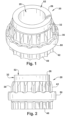
- a two piece press fit mounting bushing 20 is shown used for mounting a printed circuit board ("PCB") 22 to a structure.
- the two piece mounting bushing 20 includes an inner cylindrical piece 26 having a through bore 28.
- the inner cylindrical piece 26 is made from metal.
- a portion 30 of the outer wall 32 of the inner piece 26 has a knurled surface or, at least, a surface that has a rough texture.
- the inner piece 26 could be formed through machining, cold forming, or other metal forming processes with the knurled surface.
- the two piece mounting bushing 20 further includes an outer piece 36 that circumferentially covers at least an axial portion of the inner cylindrical piece 26 commensurate with the knurled surface.
- the outer piece 36 is made from plastic and is molded to the outer wall 32 and in contact with the knurled portion 30 so as to be adhered and fixed to the inner piece 26.
- the knurled surface, or otherwise textured surface of the inner piece provides mechanical retention between the outer piece 36 and the inner piece 26.
- the outer piece being plastic electrically isolates the inner piece from the printed circuit board 22.
- the outer piece 36 of the two piece bushing 20 includes a main body portion 40 and a plurality of radially extending retaining members 42 circumferentially and equally spaced around the main body portion 40.
- the radially extending retaining members 42 are substantially V-shaped in cross section but could take other forms.
- the retaining ring 50 radially extends outward from the main body portion 40.
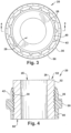
- a first end 52 of the two piece mounting bushing 20 is inserted, i.e., press fit, into an opening 56 of the PCB 22.
- the outside radial diameter of the radially extending retaining members 42 is slightly greater than the diameter of the opening 56 of the PCB 22 such that the bushing 20 must be press fit into the opening with sufficient force applied against end 58. Force would be continuously applied until the retaining ring 50 contacts the PCB 22.
- the radially extending retaining members 42 deform slightly and form a tight press fit engagement, i.e., interference fit, with the PCB 22.
- a bolt may then be inserted through the opening 28 so as to secure the PCB 22 to a mounting structure via a nut on the end of the bolt.
- the press fit mounting bushing were made entirely of metal, such a bushing would cause stress in the PCB board when inserted into the PCB. Also, if the PCB would include a plurality of all metal bushings, the accumulated stress caused by the metal bushings could result in a bowing of the PCB.
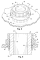
- the PCB 22 includes circuitry 64 mounted to the PCB 22.
- the circuitry 64 could include vehicle crash sensors such as an accelerometer or a pressure sensor.
- the bushing 20 is mounted to the PCB 22 as described above with regard to Figs. 1-6 .
- the two piece bushing 20 is press fit into the circuit board 22 as described above prior to an overmolding process.
- a soft plastic material 68 is molded over the circuitry 64 and a portion of the PCB 22.
- a hard plastic material 72 is then overmolded the soft plastic material 68, the exposed portions of the PCB 22 and the two piece bushing 20.
- the hard plastic material forms a rigid mounting case 74 that is formed, i.e., molded, into any desired shape.
- the rigid mounting case 78 is then, in turn, secured to a mounting structure 80, such as a mounting beam in a vehicle, using a bolt 82 and associated nut 84 through the two piece bushing 20.
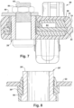
- FIG. 8 another example embodiment is shown of the present invention using a modified two piece press fit bushing 20' for mounting to a PCB 22.
- the bushing 20' has an inner member 26' made of metal and outer plastic member 36' secured to a knurled portion of the inner member in a similar manner as described above.
- the inner member 26' includes a stepped flange portion 90 that provides an additional contact surface to enhance the retention characteristics between the inner member 26' and the outer member 36' of the two piece bushing 20'.
- the retention members have been described, in accordance with one example embodiment, as being V-shaped in cross section. Other shapes or patterns could also be used. Such improvements, changes and modifications within the skill of the art are intended to be covered by the invention provided that they fall within the scope of the claims.
Landscapes
- Engineering & Computer Science (AREA)
- Microelectronics & Electronic Packaging (AREA)
- Multi-Conductor Connections (AREA)
- Mounting Of Printed Circuit Boards And The Like (AREA)
- Casings For Electric Apparatus (AREA)
Claims (8)
- Agencement de montage de carte de circuit imprimé (60) comprenant :une carte de circuit imprimé (22) ; etune douille de montage à ajustement serré (20 ; 20') comprenant une pièce intérieure cylindrique (26 ; 26') et une pièce extérieure (36 ; 36') fixée à ladite pièce intérieure (26 ; 26'), ladite pièce extérieure (36 ; 36') ayant une pluralité d'éléments déformables faisant saillie radialement (42), ladite carte de circuit imprimé (22) ayant une ouverture cylindrique (56) ayant un diamètre inférieur à un diamètre extérieur desdits éléments déformables faisant saillie radialement (42) de ladite pièce extérieure (36 ; 36'), lesdits éléments déformables (42) se déformant lorsque ladite douille de montage (20 ; 20') est poussée dans ladite ouverture cylindrique (56) de ladite carte de circuit imprimé (22) de manière à maintenir ladite douille de montage (20 ; 20') sur ladite carte de circuit imprimé (22),dans lequel ladite pièce intérieure cylindrique (26) est faite de métal et a une surface extérieure moletée ou, au moins, une surface qui a une texture rugueuse, etdans lequel ladite pièce extérieure (36) est en plastique et est fixée à ladite surface extérieure moletée ou à ladite surface ayant une texture rugueuse de ladite pièce intérieure cylindrique (26).
- Agencement de montage de carte de circuit imprimé (60) selon la revendication 1, dans lequel ladite carte de circuit imprimé (22) et ladite douille de montage à ajustement serré (20) sont surmoulées avec une matière plastique (68, 72) de manière à protéger tout circuit sur ladite carte de circuit imprimé (22) et à fournir un boîtier (74).
- Agencement de montage de carte de circuit imprimé (60) selon la revendication 2, dans lequel ledit boîtier (74) est monté sur une structure en utilisant une fixation filetée (82).
- Agencement de montage de carte de circuit imprimé (60) selon la revendication 1, dans lequel ladite pièce externe (36) est moulée sur ladite pièce interne (26).
- Agencement de montage de carte de circuit imprimé (60) selon la revendication 1, dans lequel lesdits éléments déformables (42) ont une section transversale généralement en forme de V.
- Agencement de montage de carte de circuit imprimé (60) selon la revendication 1, dans lequel ladite pièce intérieure cylindrique (26') a une surface extérieure moletée et une surface étagée et dans lequel ladite pièce extérieure (36') est fixée à ladite surface moletée et à ladite surface étagée de ladite pièce intérieure cylindrique (26').
- Agencement de montage de carte de circuit imprimé (60) selon la revendication 6, dans lequel ladite pièce extérieure (36') est moulée sur ladite pièce intérieure (26').
- Agencement de montage de carte de circuit imprimé (60) selon la revendication 6, dans lequel lesdits éléments déformables ont une section transversale généralement en forme de V.
Applications Claiming Priority (1)
| Application Number | Priority Date | Filing Date | Title |
|---|---|---|---|
| US14/199,294 US9648721B2 (en) | 2014-03-06 | 2014-03-06 | Apparatus for mounting a printed circuit board |
Publications (2)
| Publication Number | Publication Date |
|---|---|
| EP2916632A1 EP2916632A1 (fr) | 2015-09-09 |
| EP2916632B1 true EP2916632B1 (fr) | 2023-04-05 |
Family
ID=53180500
Family Applications (1)
| Application Number | Title | Priority Date | Filing Date |
|---|---|---|---|
| EP15157937.2A Active EP2916632B1 (fr) | 2014-03-06 | 2015-03-06 | Appareil de fixation d'une carte de circuit imprimé |
Country Status (4)
| Country | Link |
|---|---|
| US (1) | US9648721B2 (fr) |
| EP (1) | EP2916632B1 (fr) |
| KR (1) | KR101702746B1 (fr) |
| CN (1) | CN105101722B (fr) |
Families Citing this family (3)
| Publication number | Priority date | Publication date | Assignee | Title |
|---|---|---|---|---|
| CN108934132B (zh) | 2017-05-25 | 2021-08-06 | 法雷奥汽车内部控制(深圳)有限公司 | 印刷电路板组件及其封装方法和机动车辆 |
| JP6915555B2 (ja) * | 2018-01-23 | 2021-08-04 | トヨタ自動車株式会社 | 部品の接合構造 |
| DE102018206536B4 (de) * | 2018-04-27 | 2024-05-16 | Bayerische Motoren Werke Aktiengesellschaft | Verfahren zum Herstellen einer Welle-Nabeverbindung und Kraftfahrzeugwelle mit einer solchen Verbindung |
Citations (2)
| Publication number | Priority date | Publication date | Assignee | Title |
|---|---|---|---|---|
| DE3539361A1 (de) * | 1985-11-06 | 1987-05-14 | Siemens Ag | Verbindungselement fuer elektronische baugruppen in sandwich-bauweise |
| DE102007036418A1 (de) * | 2007-08-02 | 2008-04-30 | Daimler Ag | Befestigungsanordnung |
Family Cites Families (11)
| Publication number | Priority date | Publication date | Assignee | Title |
|---|---|---|---|---|
| US4521004A (en) * | 1982-10-27 | 1985-06-04 | Caldwell William F | Vibration-isolating mounting with load-directing chamfer |
| US5879115A (en) | 1992-05-22 | 1999-03-09 | Unimation, Inc. | Method and insert for connecting components to plastic members |
| US5363276A (en) | 1993-09-01 | 1994-11-08 | Ncr Corporation | Apparatus for containing and supporting electronic components |
| US6180883B1 (en) | 1999-02-08 | 2001-01-30 | General Motors Corporation | Cast in situ retention features for a press fit assembly |
| US6395985B1 (en) * | 1999-11-23 | 2002-05-28 | Sapco | Sealed electrical terminal with anti-rotation locking system |
| EP1443331A3 (fr) | 2003-02-03 | 2005-10-12 | Denso Corporation | Dispositif capteur et empaquetage en céramique pour le montage de composants électroniques |
| CN1816700A (zh) * | 2003-07-03 | 2006-08-09 | 库博标准汽车配件有限公司 | 塑料快速卡合的中轴承隔离座及其制造和组装方法 |
| KR100662099B1 (ko) | 2006-05-04 | 2006-12-27 | 삼양기전(주) | 철근연결구 |
| DE102008000442A1 (de) * | 2008-02-29 | 2009-09-03 | Robert Bosch Gmbh | Platinenanordnung |
| US8156797B2 (en) * | 2008-07-28 | 2012-04-17 | Trw Automotive U.S. Llc | Method and apparatus for overmolding a tire pressure monitor sensor |
| JP5685187B2 (ja) | 2008-07-28 | 2015-03-18 | ティーアールダブリュー・オートモーティブ・ユーエス・エルエルシー | 車両衝突センサを収納するための方法及び装置 |
-
2014
- 2014-03-06 US US14/199,294 patent/US9648721B2/en active Active
-
2015
- 2015-03-02 KR KR1020150028886A patent/KR101702746B1/ko active Active
- 2015-03-05 CN CN201510097932.7A patent/CN105101722B/zh active Active
- 2015-03-06 EP EP15157937.2A patent/EP2916632B1/fr active Active
Patent Citations (2)
| Publication number | Priority date | Publication date | Assignee | Title |
|---|---|---|---|---|
| DE3539361A1 (de) * | 1985-11-06 | 1987-05-14 | Siemens Ag | Verbindungselement fuer elektronische baugruppen in sandwich-bauweise |
| DE102007036418A1 (de) * | 2007-08-02 | 2008-04-30 | Daimler Ag | Befestigungsanordnung |
Also Published As
| Publication number | Publication date |
|---|---|
| CN105101722A (zh) | 2015-11-25 |
| CN105101722B (zh) | 2018-05-15 |
| KR101702746B1 (ko) | 2017-02-06 |
| US9648721B2 (en) | 2017-05-09 |
| KR20150105215A (ko) | 2015-09-16 |
| EP2916632A1 (fr) | 2015-09-09 |
| US20150257248A1 (en) | 2015-09-10 |
Similar Documents
| Publication | Publication Date | Title |
|---|---|---|
| EP2916632B1 (fr) | Appareil de fixation d'une carte de circuit imprimé | |
| CN103104581A (zh) | 螺钉组装元件 | |
| US10062959B2 (en) | Mount for vehicular roof antenna | |
| JP2014168983A (ja) | 車両用電子制御ユニット及びその製造方法 | |
| DE102016205240B3 (de) | Verfahren zum Herstellen eines Ultraschallsensors und Ultraschallensor | |
| EP2472234A3 (fr) | Composants d'assemblage de détection et procédés pour les assembler, les monter et les orienter | |
| CN104121934B (zh) | 传感器单元 | |
| AU2017268298B2 (en) | Direct tension indicating apparatus | |
| CN107110193A (zh) | 用于将扭矩导入塑料外壳的金属固定件 | |
| US11193522B2 (en) | Shear bolt | |
| JP2010107047A (ja) | 圧入式スペーサナット | |
| KR20170042641A (ko) | 전기 장치 | |
| KR20170075989A (ko) | 차량용 대쉬 그로멧의 프로텍터 | |
| US9696334B2 (en) | Wheel speed sensor | |
| US20130266399A1 (en) | Mounting structure | |
| EP3179561A1 (fr) | Dispositif pour fixer une borne de connexion électrique à un support | |
| EP3006746B1 (fr) | Fixation intégrée pour composants en plastique | |
| JP2001012440A (ja) | ネジ締結体の緩み止め構造及び被締結材の緩み止め構造 | |
| KR20190055626A (ko) | 절연 와셔 | |
| US20170297630A1 (en) | Integrated fastener for instrumentation cluster | |
| US20170218987A1 (en) | Screw boss locators and torque resistors | |
| DE102012218901A1 (de) | Sensorvorrichtung mit Positioniereinrichtung | |
| WO2019101390A1 (fr) | Unité de détection pour véhicule | |
| KR20200028936A (ko) | 압력 매체 조립체 | |
| KR101634542B1 (ko) | 회전체 측정용 센서조립체 및 그 제조방법 |
Legal Events
| Date | Code | Title | Description |
|---|---|---|---|
| PUAI | Public reference made under article 153(3) epc to a published international application that has entered the european phase |
Free format text: ORIGINAL CODE: 0009012 |
|
| AK | Designated contracting states |
Kind code of ref document: A1 Designated state(s): AL AT BE BG CH CY CZ DE DK EE ES FI FR GB GR HR HU IE IS IT LI LT LU LV MC MK MT NL NO PL PT RO RS SE SI SK SM TR |
|
| AX | Request for extension of the european patent |
Extension state: BA ME |
|
| 17P | Request for examination filed |
Effective date: 20160309 |
|
| RBV | Designated contracting states (corrected) |
Designated state(s): AL AT BE BG CH CY CZ DE DK EE ES FI FR GB GR HR HU IE IS IT LI LT LU LV MC MK MT NL NO PL PT RO RS SE SI SK SM TR |
|
| STAA | Information on the status of an ep patent application or granted ep patent |
Free format text: STATUS: EXAMINATION IS IN PROGRESS |
|
| 17Q | First examination report despatched |
Effective date: 20190614 |
|
| GRAP | Despatch of communication of intention to grant a patent |
Free format text: ORIGINAL CODE: EPIDOSNIGR1 |
|
| STAA | Information on the status of an ep patent application or granted ep patent |
Free format text: STATUS: GRANT OF PATENT IS INTENDED |
|
| INTG | Intention to grant announced |
Effective date: 20221019 |
|
| GRAS | Grant fee paid |
Free format text: ORIGINAL CODE: EPIDOSNIGR3 |
|
| GRAA | (expected) grant |
Free format text: ORIGINAL CODE: 0009210 |
|
| STAA | Information on the status of an ep patent application or granted ep patent |
Free format text: STATUS: THE PATENT HAS BEEN GRANTED |
|
| AK | Designated contracting states |
Kind code of ref document: B1 Designated state(s): AL AT BE BG CH CY CZ DE DK EE ES FI FR GB GR HR HU IE IS IT LI LT LU LV MC MK MT NL NO PL PT RO RS SE SI SK SM TR |
|
| REG | Reference to a national code |
Ref country code: GB Ref legal event code: FG4D |
|
| REG | Reference to a national code |
Ref country code: DE Ref legal event code: R096 Ref document number: 602015083024 Country of ref document: DE |
|
| REG | Reference to a national code |
Ref country code: CH Ref legal event code: EP |
|
| REG | Reference to a national code |
Ref country code: AT Ref legal event code: REF Ref document number: 1559266 Country of ref document: AT Kind code of ref document: T Effective date: 20230415 |
|
| REG | Reference to a national code |
Ref country code: IE Ref legal event code: FG4D |
|
| P01 | Opt-out of the competence of the unified patent court (upc) registered |
Effective date: 20230524 |
|
| REG | Reference to a national code |
Ref country code: LT Ref legal event code: MG9D |
|
| REG | Reference to a national code |
Ref country code: NL Ref legal event code: MP Effective date: 20230405 |
|
| REG | Reference to a national code |
Ref country code: AT Ref legal event code: MK05 Ref document number: 1559266 Country of ref document: AT Kind code of ref document: T Effective date: 20230405 |
|
| PG25 | Lapsed in a contracting state [announced via postgrant information from national office to epo] |
Ref country code: NL Free format text: LAPSE BECAUSE OF FAILURE TO SUBMIT A TRANSLATION OF THE DESCRIPTION OR TO PAY THE FEE WITHIN THE PRESCRIBED TIME-LIMIT Effective date: 20230405 |
|
| PG25 | Lapsed in a contracting state [announced via postgrant information from national office to epo] |
Ref country code: SE Free format text: LAPSE BECAUSE OF FAILURE TO SUBMIT A TRANSLATION OF THE DESCRIPTION OR TO PAY THE FEE WITHIN THE PRESCRIBED TIME-LIMIT Effective date: 20230405 Ref country code: PT Free format text: LAPSE BECAUSE OF FAILURE TO SUBMIT A TRANSLATION OF THE DESCRIPTION OR TO PAY THE FEE WITHIN THE PRESCRIBED TIME-LIMIT Effective date: 20230807 Ref country code: NO Free format text: LAPSE BECAUSE OF FAILURE TO SUBMIT A TRANSLATION OF THE DESCRIPTION OR TO PAY THE FEE WITHIN THE PRESCRIBED TIME-LIMIT Effective date: 20230705 Ref country code: ES Free format text: LAPSE BECAUSE OF FAILURE TO SUBMIT A TRANSLATION OF THE DESCRIPTION OR TO PAY THE FEE WITHIN THE PRESCRIBED TIME-LIMIT Effective date: 20230405 Ref country code: AT Free format text: LAPSE BECAUSE OF FAILURE TO SUBMIT A TRANSLATION OF THE DESCRIPTION OR TO PAY THE FEE WITHIN THE PRESCRIBED TIME-LIMIT Effective date: 20230405 |
|
| PG25 | Lapsed in a contracting state [announced via postgrant information from national office to epo] |
Ref country code: RS Free format text: LAPSE BECAUSE OF FAILURE TO SUBMIT A TRANSLATION OF THE DESCRIPTION OR TO PAY THE FEE WITHIN THE PRESCRIBED TIME-LIMIT Effective date: 20230405 Ref country code: PL Free format text: LAPSE BECAUSE OF FAILURE TO SUBMIT A TRANSLATION OF THE DESCRIPTION OR TO PAY THE FEE WITHIN THE PRESCRIBED TIME-LIMIT Effective date: 20230405 Ref country code: LV Free format text: LAPSE BECAUSE OF FAILURE TO SUBMIT A TRANSLATION OF THE DESCRIPTION OR TO PAY THE FEE WITHIN THE PRESCRIBED TIME-LIMIT Effective date: 20230405 Ref country code: LT Free format text: LAPSE BECAUSE OF FAILURE TO SUBMIT A TRANSLATION OF THE DESCRIPTION OR TO PAY THE FEE WITHIN THE PRESCRIBED TIME-LIMIT Effective date: 20230405 Ref country code: IS Free format text: LAPSE BECAUSE OF FAILURE TO SUBMIT A TRANSLATION OF THE DESCRIPTION OR TO PAY THE FEE WITHIN THE PRESCRIBED TIME-LIMIT Effective date: 20230805 Ref country code: HR Free format text: LAPSE BECAUSE OF FAILURE TO SUBMIT A TRANSLATION OF THE DESCRIPTION OR TO PAY THE FEE WITHIN THE PRESCRIBED TIME-LIMIT Effective date: 20230405 Ref country code: GR Free format text: LAPSE BECAUSE OF FAILURE TO SUBMIT A TRANSLATION OF THE DESCRIPTION OR TO PAY THE FEE WITHIN THE PRESCRIBED TIME-LIMIT Effective date: 20230706 Ref country code: AL Free format text: LAPSE BECAUSE OF FAILURE TO SUBMIT A TRANSLATION OF THE DESCRIPTION OR TO PAY THE FEE WITHIN THE PRESCRIBED TIME-LIMIT Effective date: 20230405 |
|
| PG25 | Lapsed in a contracting state [announced via postgrant information from national office to epo] |
Ref country code: FI Free format text: LAPSE BECAUSE OF FAILURE TO SUBMIT A TRANSLATION OF THE DESCRIPTION OR TO PAY THE FEE WITHIN THE PRESCRIBED TIME-LIMIT Effective date: 20230405 |
|
| REG | Reference to a national code |
Ref country code: DE Ref legal event code: R097 Ref document number: 602015083024 Country of ref document: DE |
|
| PG25 | Lapsed in a contracting state [announced via postgrant information from national office to epo] |
Ref country code: SK Free format text: LAPSE BECAUSE OF FAILURE TO SUBMIT A TRANSLATION OF THE DESCRIPTION OR TO PAY THE FEE WITHIN THE PRESCRIBED TIME-LIMIT Effective date: 20230405 |
|
| PG25 | Lapsed in a contracting state [announced via postgrant information from national office to epo] |
Ref country code: SM Free format text: LAPSE BECAUSE OF FAILURE TO SUBMIT A TRANSLATION OF THE DESCRIPTION OR TO PAY THE FEE WITHIN THE PRESCRIBED TIME-LIMIT Effective date: 20230405 Ref country code: SK Free format text: LAPSE BECAUSE OF FAILURE TO SUBMIT A TRANSLATION OF THE DESCRIPTION OR TO PAY THE FEE WITHIN THE PRESCRIBED TIME-LIMIT Effective date: 20230405 Ref country code: RO Free format text: LAPSE BECAUSE OF FAILURE TO SUBMIT A TRANSLATION OF THE DESCRIPTION OR TO PAY THE FEE WITHIN THE PRESCRIBED TIME-LIMIT Effective date: 20230405 Ref country code: EE Free format text: LAPSE BECAUSE OF FAILURE TO SUBMIT A TRANSLATION OF THE DESCRIPTION OR TO PAY THE FEE WITHIN THE PRESCRIBED TIME-LIMIT Effective date: 20230405 Ref country code: DK Free format text: LAPSE BECAUSE OF FAILURE TO SUBMIT A TRANSLATION OF THE DESCRIPTION OR TO PAY THE FEE WITHIN THE PRESCRIBED TIME-LIMIT Effective date: 20230405 Ref country code: CZ Free format text: LAPSE BECAUSE OF FAILURE TO SUBMIT A TRANSLATION OF THE DESCRIPTION OR TO PAY THE FEE WITHIN THE PRESCRIBED TIME-LIMIT Effective date: 20230405 |
|
| PLBE | No opposition filed within time limit |
Free format text: ORIGINAL CODE: 0009261 |
|
| STAA | Information on the status of an ep patent application or granted ep patent |
Free format text: STATUS: NO OPPOSITION FILED WITHIN TIME LIMIT |
|
| 26N | No opposition filed |
Effective date: 20240108 |
|
| PG25 | Lapsed in a contracting state [announced via postgrant information from national office to epo] |
Ref country code: SI Free format text: LAPSE BECAUSE OF FAILURE TO SUBMIT A TRANSLATION OF THE DESCRIPTION OR TO PAY THE FEE WITHIN THE PRESCRIBED TIME-LIMIT Effective date: 20230405 |
|
| PG25 | Lapsed in a contracting state [announced via postgrant information from national office to epo] |
Ref country code: SI Free format text: LAPSE BECAUSE OF FAILURE TO SUBMIT A TRANSLATION OF THE DESCRIPTION OR TO PAY THE FEE WITHIN THE PRESCRIBED TIME-LIMIT Effective date: 20230405 Ref country code: IT Free format text: LAPSE BECAUSE OF FAILURE TO SUBMIT A TRANSLATION OF THE DESCRIPTION OR TO PAY THE FEE WITHIN THE PRESCRIBED TIME-LIMIT Effective date: 20230405 |
|
| REG | Reference to a national code |
Ref country code: CH Ref legal event code: PL |
|
| PG25 | Lapsed in a contracting state [announced via postgrant information from national office to epo] |
Ref country code: BG Free format text: LAPSE BECAUSE OF FAILURE TO SUBMIT A TRANSLATION OF THE DESCRIPTION OR TO PAY THE FEE WITHIN THE PRESCRIBED TIME-LIMIT Effective date: 20230405 |
|
| PG25 | Lapsed in a contracting state [announced via postgrant information from national office to epo] |
Ref country code: LU Free format text: LAPSE BECAUSE OF NON-PAYMENT OF DUE FEES Effective date: 20240306 |
|
| PG25 | Lapsed in a contracting state [announced via postgrant information from national office to epo] |
Ref country code: MC Free format text: LAPSE BECAUSE OF FAILURE TO SUBMIT A TRANSLATION OF THE DESCRIPTION OR TO PAY THE FEE WITHIN THE PRESCRIBED TIME-LIMIT Effective date: 20230405 |
|
| PG25 | Lapsed in a contracting state [announced via postgrant information from national office to epo] |
Ref country code: MC Free format text: LAPSE BECAUSE OF FAILURE TO SUBMIT A TRANSLATION OF THE DESCRIPTION OR TO PAY THE FEE WITHIN THE PRESCRIBED TIME-LIMIT Effective date: 20230405 Ref country code: LU Free format text: LAPSE BECAUSE OF NON-PAYMENT OF DUE FEES Effective date: 20240306 Ref country code: BG Free format text: LAPSE BECAUSE OF FAILURE TO SUBMIT A TRANSLATION OF THE DESCRIPTION OR TO PAY THE FEE WITHIN THE PRESCRIBED TIME-LIMIT Effective date: 20230405 |
|
| REG | Reference to a national code |
Ref country code: BE Ref legal event code: MM Effective date: 20240331 |
|
| PG25 | Lapsed in a contracting state [announced via postgrant information from national office to epo] |
Ref country code: BE Free format text: LAPSE BECAUSE OF NON-PAYMENT OF DUE FEES Effective date: 20240331 |
|
| PG25 | Lapsed in a contracting state [announced via postgrant information from national office to epo] |
Ref country code: FR Free format text: LAPSE BECAUSE OF NON-PAYMENT OF DUE FEES Effective date: 20240331 |
|
| PG25 | Lapsed in a contracting state [announced via postgrant information from national office to epo] |
Ref country code: IE Free format text: LAPSE BECAUSE OF NON-PAYMENT OF DUE FEES Effective date: 20240306 |
|
| PG25 | Lapsed in a contracting state [announced via postgrant information from national office to epo] |
Ref country code: IE Free format text: LAPSE BECAUSE OF NON-PAYMENT OF DUE FEES Effective date: 20240306 Ref country code: FR Free format text: LAPSE BECAUSE OF NON-PAYMENT OF DUE FEES Effective date: 20240331 Ref country code: BE Free format text: LAPSE BECAUSE OF NON-PAYMENT OF DUE FEES Effective date: 20240331 Ref country code: CH Free format text: LAPSE BECAUSE OF NON-PAYMENT OF DUE FEES Effective date: 20240331 |
|
| PG25 | Lapsed in a contracting state [announced via postgrant information from national office to epo] |
Ref country code: CY Free format text: LAPSE BECAUSE OF FAILURE TO SUBMIT A TRANSLATION OF THE DESCRIPTION OR TO PAY THE FEE WITHIN THE PRESCRIBED TIME-LIMIT; INVALID AB INITIO Effective date: 20150306 |
|
| PG25 | Lapsed in a contracting state [announced via postgrant information from national office to epo] |
Ref country code: HU Free format text: LAPSE BECAUSE OF FAILURE TO SUBMIT A TRANSLATION OF THE DESCRIPTION OR TO PAY THE FEE WITHIN THE PRESCRIBED TIME-LIMIT; INVALID AB INITIO Effective date: 20150306 |
|
| PG25 | Lapsed in a contracting state [announced via postgrant information from national office to epo] |
Ref country code: TR Free format text: LAPSE BECAUSE OF FAILURE TO SUBMIT A TRANSLATION OF THE DESCRIPTION OR TO PAY THE FEE WITHIN THE PRESCRIBED TIME-LIMIT Effective date: 20230405 |
|
| PGFP | Annual fee paid to national office [announced via postgrant information from national office to epo] |
Ref country code: GB Payment date: 20260106 Year of fee payment: 12 |
|
| PGFP | Annual fee paid to national office [announced via postgrant information from national office to epo] |
Ref country code: DE Payment date: 20260102 Year of fee payment: 12 |