EP2904360B1 - Laser power and energy sensor utilizing anisotropic thermoelectric material - Google Patents
Laser power and energy sensor utilizing anisotropic thermoelectric material Download PDFInfo
- Publication number
- EP2904360B1 EP2904360B1 EP13773581.7A EP13773581A EP2904360B1 EP 2904360 B1 EP2904360 B1 EP 2904360B1 EP 13773581 A EP13773581 A EP 13773581A EP 2904360 B1 EP2904360 B1 EP 2904360B1
- Authority
- EP
- European Patent Office
- Prior art keywords
- sensor
- layer
- radiation
- laser
- radiation sensor
- Prior art date
- Legal status (The legal status is an assumption and is not a legal conclusion. Google has not performed a legal analysis and makes no representation as to the accuracy of the status listed.)
- Active
Links
Images


Classifications
-
- H—ELECTRICITY
- H10—SEMICONDUCTOR DEVICES; ELECTRIC SOLID-STATE DEVICES NOT OTHERWISE PROVIDED FOR
- H10F—INORGANIC SEMICONDUCTOR DEVICES SENSITIVE TO INFRARED RADIATION, LIGHT, ELECTROMAGNETIC RADIATION OF SHORTER WAVELENGTH OR CORPUSCULAR RADIATION
- H10F77/00—Constructional details of devices covered by this subclass
- H10F77/10—Semiconductor bodies
- H10F77/16—Material structures, e.g. crystalline structures, film structures or crystal plane orientations
- H10F77/162—Non-monocrystalline materials, e.g. semiconductor particles embedded in insulating materials
- H10F77/164—Polycrystalline semiconductors
-
- G—PHYSICS
- G01—MEASURING; TESTING
- G01J—MEASUREMENT OF INTENSITY, VELOCITY, SPECTRAL CONTENT, POLARISATION, PHASE OR PULSE CHARACTERISTICS OF INFRARED, VISIBLE OR ULTRAVIOLET LIGHT; COLORIMETRY; RADIATION PYROMETRY
- G01J1/00—Photometry, e.g. photographic exposure meter
- G01J1/42—Photometry, e.g. photographic exposure meter using electric radiation detectors
- G01J1/4257—Photometry, e.g. photographic exposure meter using electric radiation detectors applied to monitoring the characteristics of a beam, e.g. laser beam, headlamp beam
-
- G—PHYSICS
- G01—MEASURING; TESTING
- G01J—MEASUREMENT OF INTENSITY, VELOCITY, SPECTRAL CONTENT, POLARISATION, PHASE OR PULSE CHARACTERISTICS OF INFRARED, VISIBLE OR ULTRAVIOLET LIGHT; COLORIMETRY; RADIATION PYROMETRY
- G01J5/00—Radiation pyrometry, e.g. infrared or optical thermometry
- G01J5/02—Constructional details
- G01J5/04—Casings
- G01J5/046—Materials; Selection of thermal materials
-
- G—PHYSICS
- G01—MEASURING; TESTING
- G01J—MEASUREMENT OF INTENSITY, VELOCITY, SPECTRAL CONTENT, POLARISATION, PHASE OR PULSE CHARACTERISTICS OF INFRARED, VISIBLE OR ULTRAVIOLET LIGHT; COLORIMETRY; RADIATION PYROMETRY
- G01J5/00—Radiation pyrometry, e.g. infrared or optical thermometry
- G01J5/10—Radiation pyrometry, e.g. infrared or optical thermometry using electric radiation detectors
- G01J5/12—Radiation pyrometry, e.g. infrared or optical thermometry using electric radiation detectors using thermoelectric elements, e.g. thermocouples
-
- G—PHYSICS
- G01—MEASURING; TESTING
- G01K—MEASURING TEMPERATURE; MEASURING QUANTITY OF HEAT; THERMALLY-SENSITIVE ELEMENTS NOT OTHERWISE PROVIDED FOR
- G01K17/00—Measuring quantity of heat
- G01K17/003—Measuring quantity of heat for measuring the power of light beams, e.g. laser beams
Definitions
- the present invention relates in general to laser-radiation detectors.
- the invention relates in particular to a laser-radiation detector that utilizes a transverse thermoelectric effect.
- Laser-radiation detectors are used in laser applications wherein laser-radiation power needs to be measured or monitored.
- the power measurement may be required from simple record-keeping or as part of some closed loop control arrangement.
- Commonly used radiation detectors are based on either photodiodes or thermopiles.
- the photodiode-based sensors detect laser-radiation by converting photon energy of radiation to be measured into an electron-hole pairs in the photo-diode thereby generating a corresponding current, which is used a measure of laser-radiation power.
- Photodiodes sensors have a relatively fast temporal response, with rise times typically less than 1 microsecond ( ⁇ s).
- a disadvantage of photodiode detectors is a limited spectral response. This spectral response is determined by the particular semiconductor materials used for forming the photodiode.
- photodiode sensors based on silicon have a spectral acceptance bandwidth between about 0.2 micrometers ( ⁇ m) and about 2.0 ⁇ m.
- a second limitation of a photodiode is relatively low optical power saturation. Photodiodes are typically limited to direct measurement of laser powers of less than 100 milliwatts (mW).
- Thermopile sensors include a solid element which absorbs the radiation, thereby heating the element.
- One or more thermocouples in contact with the element create a current or voltage representative of the laser-radiation power incident on the element.
- Thermopile sensors have a slow response time relative to photodiode detectors. The response time is dependent on the size of the sensor-element.
- radial thermopiles with apertures of 19 millimeters (mm) and 200 mm have response times of approximately 1 second and 30 seconds respectively.
- Spectral response of the thermopile sensors depends on the absorption spectrum of the sensor. With a suitable choice and configuration of the sensor, the spectral response can extend from ultraviolet (UV) wavelengths to far infrared wavelengths. With a sufficient heat sink, thermopile sensors can measure lasers power up to about 10 kilowatts (kW).
- One relatively new detector type which has been proposed to offer a temporal response comparable to a photodiode detector and a spectral response comparable with a thermopile detector is based on using a layer of an anisotropic transverse thermoelectric material as a detector element.
- Such an anisotropic layer is formed by growing the material in an oriented polycrystalline crystalline form, with crystals inclined non-orthogonally to the plane of the layer.
- the anisotropic layer absorbs radiation to be measured thereby heating the layer. This creates a thermal gradient through the anisotropic material in a direction perpendicular to the layer. This thermal gradient, in turn, creates an electric field orthogonal to the thermal gradient. The electric field is proportional to the intensity of incident radiation absorbed.
- a detector may be referred to as a transverse thermoelectric effect detector. If the anisotropic layer is made sufficiently thin, for example only a few micrometers thick, the response time of the detector will be comparable with that of a photodiode detector. Spectral response is limited only by the absorbance of the anisotropic material. A disadvantage is that the transverse thermoelectric effect is relatively weak compared to the response of a photodiode.
- Oriented polycrystalline layers can be deposited by a well-known inclined substrate deposition (ISD) process. This process is described in detail in U.S. Patent No. 6,265,353 and in U.S. Patent No. 6,638,598 . Oriented polycrystalline layers have also been grown by a (somewhat less versatile) ion-beam assisted deposition (IBAD) process.
- IBAD ion-beam assisted deposition
- Takahashi detector allows the anisotropic material layers to remain thin, while increasing the amount of light absorbed, but requires a transparent crystalline substrate polished on both sides, at costs potentially prohibitive for most commercial applications. Further, the Takashi detector arrangement isolates the crystalline substrate limiting the ability to heat-sink the substrate. This limits the_power-handling capability of the detector to a maximum power of less than about 10 Watts (W), and may lead to a non-linear response.
- W 10 Watts
- thermoelectric laser detectors with a multi-layered structure.
- the detector may include a heat sink, and the use of a copper block, which may be water-cooled, is described.
- US patent No. US 5823682 describes a thermoelectric sensor for measuring the thermal power of radiation.
- the detector includes at least one sensor element of a crystalline solid such as a high temperature superconductor, provided on one surface of a substrate.
- the detector may also include a cooling channel through which a coolant, such as water, can flow.
- FIG. 1 schematically illustrates a preferred embodiment 30 of a transverse thermoelectric sensor in accordance with the present invention.
- Sensor 30 includes a substrate 32 of a highly thermally conductive material.
- a preferred material for substrate 32 is copper (Cu). Copper is a preferred material due to its high thermal conductivity and relatively low cost.
- Substrate 32 has a polished surface 32A, preferably having a RMS roughness less than about 0.5 ⁇ m. The substrate is optionally in contact with a heat-sink 48, which can be passively or actively cooled.
- An oriented polycrystalline buffer-layer 34 is deposited on a surface 32A of the substrate.
- a preferred material for buffer layer 34 is magnesium oxide (MgO).
- Other suitable buffer layer materials include yttrium stabilized zirconia (YSZ), cerium oxide (CeO 2 ).
- Buffer layer 34 has a columnar grain structure with crystal-axis (the c-axis) 46 thereof tilted at an angle ⁇ in the direction by between about 10-degrees and about 45-degrees relative to a normal 47 to substrate surface 32A.
- the a-c plane of the crystal axes is in the plane of the drawing with the crystalline b-axis perpendicular to the plane of the drawing.
- a preferred thickness for the buffer layer is between about 0.5 ⁇ m and about 3.0 ⁇ m.
- a layer 36 of sensor-material 36 is deposited on buffer layer 32.
- the inclined oriented crystal structure of the buffer layer causes the layer of sensor-material to grow in the inclined polycrystalline form necessary for providing the desired transient thermoelectric effect.
- the tilted crystalline structure is indicated I the drawing by long-dashed lines.
- the use of the buffer eliminates a need for the substrate to be crystalline, allowing the use of the preferred copper substrate.
- the crystalline orientation of the sensor layer (c-axis orientation) is comparable to that of the buffer layer, i.e., between about 10 degrees and about 45 degrees but more probably between about 15-degrees and about 40-degrees.
- the inclination angles for the buffer and sensor layers can be about the same or somewhat different angles within the stated ranges.
- the material of the sensor-layer is a material selected from the group of thermoelectric materials consisting of dysprosium barium cuprate (DyBa 2 Cu 3 O 7 -d, often abbreviated to DyBCO), strontium sodium cobaltate (Sr 0.3 Na 0.2 CoO 2 ), and strontium cobaltate (Sr 3 Co 4 O 9 ).
- Dysprosium barium cuprate is most preferred.
- a preferred thickness for sensor layer 36 is between about 5 nanometers (nm) and about 500 nm. This thickness is less than that of the buffer layer and is required for creating a high thermal gradient across the sensor layer.
- a layer 50 is deposited for protecting the sensor layer from environmental degradation.
- a protection layer is critical when DyBCO is used for sensor layer 36.
- Preferred materials for the protection layer include MgO, and silicon dioxide (SiO 2 ).
- the thermoelectric properties of DyBCO will degrade over a relatively quick time with exposure to ambient oxygen and elevated temperatures.
- strontium cobaltate and strontium sodium cobaltate are degraded by exposure to atmospheric humidity.
- a preferred thickness for protective layer 50 is between about 0.2 ⁇ m and about 2.0 ⁇ m.
- An optically black radiation-absorbing layer 42 is grown on protective layer 50.
- the absorption spectrum of this layer essentially determines the spectral response of the inventive transverse thermoelectric radiation sensor.
- Suitable materials for layer 42 include boron carbide, titanium nitride, chromium oxide, gold black, or carbon.
- the absorption layer preferably has a thickness between about 0.5 ⁇ m and about 5.0 ⁇ m. Whatever the selected material, layer 42 is preferably made sufficiently thick such that about 95% or greater of radiation is absorbed and converted to heat within the absorption layer. Incomplete absorption in layer 42 results in less than optimum thermoelectric response signal, and can result in a non-linear response.
- thermoelectric properties of sensor layer 36 When the radiation-absorber layer is heated by incident radiation a thermal gradient is formed across sensor layer 36 between the radiation-absorber layer and copper substrate 32. Because of a high anisotropy of the thermoelectric properties of sensor layer 36 resulting from the tilted crystal-axis, heat flow across the thickness of the sensor layer, generates an electric field in the sensor layer perpendicular (transverse to) to the heat-flow (thermal-gradient) direction. This transverse electric field results from significantly different values of Seebeck coefficients in the crystalline a-b and c directions for the sensor-layer material.
- Elongated electrodes 38 and 40 parallel to each other and spaced apart, are deposited on sensor layer 36 in electrical contact therewith.
- Suitable materials for the electrodes include gold (Au), platinum (Pt), silver (Ag), and palladium (Pd).
- Au gold
- Pt platinum
- Ag silver
- Pd palladium
- V x L 2 ⁇ t ⁇ T z S ab ⁇ S c sin 2 ⁇
- V x is the voltage produced between the first electrode 38 and the second electrode 40
- t is the thickness of sensor-layer 36
- ⁇ T z is the temperature differential across sensor layer 36
- ⁇ is the tilt angle of the crystalline c- axis of layer 36
- S ab and S c are the Seebeck coefficients in respectively the a-b and c crystal directions of the sensor layer
- L is the diameter of the incident beam of laser radiation.
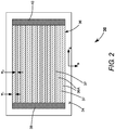
- FIG. 2 is plan-view from above schematically a preferred arrangement of sensor layer 36 in which the sensor layer is patterned into a plurality of strips 36A, each thereof extending between electrodes 38 and 40.
- the width of the strips is designated as W 1 and the width of the gaps between the strips is designated W 2 .
- the strips are aligned parallel to the c-axis direction of the sensor layer.
- the strips can be formed by photolithography and wet-etching of a continuous layer of thermoelectric material.
- Layer 36 can be defined for purposes of this description and the appended claims as a sensor-element, which term applies to continuous sensor-layer and or a layer patterned into the parallel strips of FIG. 2 or some other pattern.
- strips (c-axis aligned) of DyBCO having a width W 1 of about 300 ⁇ m, with gaps W 2 of about 50 ⁇ m therebetween, with a length between electrodes of about 33 mm and a width of about 32 mm across the pattern of strips, provided a thermoelectric signal of about 100 microvolts ( ⁇ V) when the detector was irradiated by carbon dioxide (CO 2 ) laser-radiation having a power of about 100 Watts (W).
- the thermoelectric signal voltage was about 35 ⁇ V.
- thermoelectric signal was about 60 ⁇ V.
- thermoelectric signal was about 61 ⁇ V.
- FIG. 3 is a graph schematically illustrating thermoelectric signal voltage as a function of incident CW CO 2 laser power for an example of the inventive detector having a DyBCO sensor-element patterned as depicted in FIG. 2 .
- the active area is 33 mm x 32 mm. It can be seen by comparing individual data points (circles) with the best-fit straight line that the sensor response is very linear.
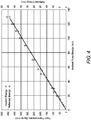
- FIG. 4 is a graph schematically illustrating peak thermoelectric voltage (circles) and reflected energy (diamond) as a function of incident pulse-energy for the detector example of FIG. 3 responsive to incident 10 nanosecond (ns) pulses from a 1064-nm solid state laser.
- the solid straight line in the graph of FIG. 4 is a best-fit to the circle (peak-voltage) data-points, indicating the same high degree of linearity of response experienced with CW radiation as in the graph of FIG. 3 .
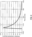
- FIG. 5 is a graph schematically illustrating thermoelectric signal as a function of time for one of the pulses of the graph of FIG. 4 .
- the response-time (rise-time) of the signal is about 640 nanoseconds, which is comparable to the response of a photodiode detector.
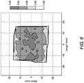
- the above-described patterning of sensor layer 36 not only improves sensitivity of the inventive detector but also the spatial uniformity of the sensitivity.
- Normalized spatial distribution of sensitivity of the detector of FIGS 3 and 4 is schematically depicted in FIG. 6 . It can be seen that the spatial uniformity over most of the useful area of the detector is about ⁇ 5%. The spatial uniformity for the same detector without a patterned sensor layer was about ⁇ 20% over the same region.
- cuprates such as dysprosium barium cuprate
- a maximum service temperature of ⁇ 350° C Based on heat Transfer calculations it is estimated that a detector using dysprosium barium cuprate as a sensor-material will be limited to measuring radiation power up to about 2 kilowatts (kW).
- Cobaltate transverse thermoelectric materials such as strontium cobaltate, in principle have service temperatures ⁇ 350° C and should allow measurement of laser power greater than 2 kW.
Landscapes
- Physics & Mathematics (AREA)
- General Physics & Mathematics (AREA)
- Spectroscopy & Molecular Physics (AREA)
- Optics & Photonics (AREA)
- Chemical & Material Sciences (AREA)
- Engineering & Computer Science (AREA)
- Combustion & Propulsion (AREA)
- Photometry And Measurement Of Optical Pulse Characteristics (AREA)
Applications Claiming Priority (3)
| Application Number | Priority Date | Filing Date | Title |
|---|---|---|---|
| US201261709060P | 2012-10-02 | 2012-10-02 | |
| US13/944,830 US9012848B2 (en) | 2012-10-02 | 2013-07-17 | Laser power and energy sensor utilizing anisotropic thermoelectric material |
| PCT/US2013/062450 WO2014055374A1 (en) | 2012-10-02 | 2013-09-27 | Laser power and energy sensor utilizing anisotropic thermoelectric material |
Publications (2)
| Publication Number | Publication Date |
|---|---|
| EP2904360A1 EP2904360A1 (en) | 2015-08-12 |
| EP2904360B1 true EP2904360B1 (en) | 2019-09-18 |
Family
ID=50384323
Family Applications (1)
| Application Number | Title | Priority Date | Filing Date |
|---|---|---|---|
| EP13773581.7A Active EP2904360B1 (en) | 2012-10-02 | 2013-09-27 | Laser power and energy sensor utilizing anisotropic thermoelectric material |
Country Status (5)
| Country | Link |
|---|---|
| US (2) | US9012848B2 (enExample) |
| EP (1) | EP2904360B1 (enExample) |
| JP (1) | JP6279589B2 (enExample) |
| CN (1) | CN104884918B (enExample) |
| WO (1) | WO2014055374A1 (enExample) |
Families Citing this family (12)
| Publication number | Priority date | Publication date | Assignee | Title |
|---|---|---|---|---|
| US9012848B2 (en) | 2012-10-02 | 2015-04-21 | Coherent, Inc. | Laser power and energy sensor utilizing anisotropic thermoelectric material |
| US9059346B2 (en) | 2012-10-02 | 2015-06-16 | Coherent, Inc. | Laser power and energy sensor utilizing anisotropic thermoelectric material |
| US20180087959A1 (en) * | 2016-09-29 | 2018-03-29 | Coherent, Inc. | Laser power and energy sensor using anisotropic thermoelectric material |
| IT201700070601A1 (it) * | 2017-06-23 | 2018-12-23 | Laser Point S R L | Rilevatore veloce di radiazione elettromagnetica. |
| IT201700070606A1 (it) * | 2017-06-23 | 2018-12-23 | Laser Point S R L | Rilevatore di radiazione elettromagnetica. |
| CN109103324A (zh) * | 2018-06-26 | 2018-12-28 | 昆明理工大学 | 一种热感生电压材料及其应用 |
| LV15536A (lv) * | 2019-04-26 | 2020-11-20 | Latvijas Universitātes Cietvielu Fizikas Institūts | Ātrdarbīgs redzamās gaismas un infrasarkanā starojuma sensors, tā izgatavošanas paņēmiens |
| CN110993778A (zh) * | 2019-12-13 | 2020-04-10 | 西南科技大学 | 一种基于薄膜横向热电效应的热流传感器 |
| CN111223983B (zh) * | 2020-02-28 | 2023-01-06 | 昆明先导新材料科技有限责任公司 | 宽禁带薄膜激光探测元件 |
| CN111710777B (zh) * | 2020-07-23 | 2025-08-26 | 中国空气动力研究与发展中心超高速空气动力研究所 | 一种以块状金属为敏感元件基底的新型原子层热电堆热流传感器及其封装工艺 |
| CN113206184B (zh) * | 2021-04-30 | 2023-04-07 | 河北大学 | 一种基于硒化铅薄膜的自驱动紫外光探测器 |
| CN115666203B (zh) | 2022-12-26 | 2023-06-16 | 山东大学 | 热流传感器 |
Family Cites Families (24)
| Publication number | Priority date | Publication date | Assignee | Title |
|---|---|---|---|---|
| US3596514A (en) | 1968-01-02 | 1971-08-03 | Coherent Radiation Lab Inc | Power meter for measurement of radiation |
| US3851174A (en) * | 1973-05-04 | 1974-11-26 | Ibm | Light detector for the nanosecond-dc pulse width range |
| US4082413A (en) | 1974-11-29 | 1978-04-04 | The Perkin-Elmer Corporation | Selective radiation absorption devices for producing heat energy |
| DE4306497C2 (de) | 1993-03-03 | 1995-01-05 | Hans Dr Lengfellner | Thermoelektrischer Detektor zur Detektion von kontinuierlicher und gepulster Strahlung und Verfahren zur Herstellung |
| JP3623001B2 (ja) | 1994-02-25 | 2005-02-23 | 住友電気工業株式会社 | 単結晶性薄膜の形成方法 |
| DE4434904A1 (de) | 1994-09-29 | 1996-06-05 | Max Planck Gesellschaft | Thermoelektrische Strahlungsdetektoren auf der Basis perovskitartiger dotierter Schichten und Übergitter |
| US5678924A (en) | 1995-09-25 | 1997-10-21 | Coherent Inc. | Power meter head for laser power measurement apparatus |
| DE19605384C1 (de) | 1996-02-14 | 1997-02-13 | Fortech Hts Gmbh | Thermoelektrischer Sensor |
| WO1998024944A1 (de) | 1996-12-06 | 1998-06-11 | THEVA DüNNSCHICHTTECHNIK GMBH | Schichtmaterial sowie vorrichtung und verfahren zum herstellen von schichtmaterial |
| DE19804487C2 (de) | 1998-02-05 | 1999-11-25 | Hans Lengfellner | Thermoelektrischer Detektor zur Detektion von kontinuierlicher und gepulster Strahlung und Verfahren zur Herstellung |
| US6361598B1 (en) | 2000-07-20 | 2002-03-26 | The University Of Chicago | Method for preparing high temperature superconductor |
| US6518609B1 (en) * | 2000-08-31 | 2003-02-11 | University Of Maryland | Niobium or vanadium substituted strontium titanate barrier intermediate a silicon underlayer and a functional metal oxide film |
| JP4135857B2 (ja) | 2001-03-27 | 2008-08-20 | 独立行政法人産業技術総合研究所 | 赤外線センサの製造方法 |
| US6579360B2 (en) | 2001-07-13 | 2003-06-17 | The University Of Chicago | Fabrication of high temperature superconductors |
| JP3874365B2 (ja) * | 2004-03-01 | 2007-01-31 | 松下電器産業株式会社 | 熱電変換デバイス、およびこれを用いた冷却方法および発電方法 |
| US7867950B2 (en) * | 2004-12-23 | 2011-01-11 | Superconductor Technologies, Inc. | RF-properties-optimized compositions of (RE)Ba2Cu3O7-δ thin film superconductors |
| WO2008056466A1 (en) * | 2006-11-10 | 2008-05-15 | Panasonic Corporation | Power generation method employing thermal power generation element, thermal power generation element and method for fabricating the same |
| CN101246055A (zh) * | 2008-03-13 | 2008-08-20 | 电子科技大学 | 钽酸锂薄膜红外探测器及制法 |
| WO2010058559A1 (ja) * | 2008-11-21 | 2010-05-27 | パナソニック株式会社 | 放射検出器および放射検出方法 |
| US8049154B2 (en) | 2009-02-20 | 2011-11-01 | Panasonic Corporation | Radiation detector with AL2O3 substrate and radiation detection method |
| JP5300102B2 (ja) * | 2009-09-03 | 2013-09-25 | 独立行政法人産業技術総合研究所 | ボロメータ用抵抗体膜 |
| JP2011243824A (ja) * | 2010-05-20 | 2011-12-01 | Panasonic Corp | 異方的熱電材料とこれを用いた放射検出器および発電デバイス |
| CN102356305A (zh) * | 2010-05-27 | 2012-02-15 | 松下电器产业株式会社 | 热电变换器件和辐射检测器以及使用它的辐射检测方法 |
| US9012848B2 (en) | 2012-10-02 | 2015-04-21 | Coherent, Inc. | Laser power and energy sensor utilizing anisotropic thermoelectric material |
-
2013
- 2013-07-17 US US13/944,830 patent/US9012848B2/en not_active Ceased
- 2013-09-27 CN CN201380051638.1A patent/CN104884918B/zh active Active
- 2013-09-27 WO PCT/US2013/062450 patent/WO2014055374A1/en not_active Ceased
- 2013-09-27 EP EP13773581.7A patent/EP2904360B1/en active Active
- 2013-09-27 JP JP2015534776A patent/JP6279589B2/ja active Active
-
2016
- 2016-05-05 US US15/147,816 patent/USRE48028E1/en active Active
Non-Patent Citations (1)
| Title |
|---|
| None * |
Also Published As
| Publication number | Publication date |
|---|---|
| JP2015537191A (ja) | 2015-12-24 |
| EP2904360A1 (en) | 2015-08-12 |
| US9012848B2 (en) | 2015-04-21 |
| CN104884918B (zh) | 2018-01-30 |
| JP6279589B2 (ja) | 2018-02-14 |
| CN104884918A (zh) | 2015-09-02 |
| US20140091304A1 (en) | 2014-04-03 |
| WO2014055374A1 (en) | 2014-04-10 |
| USRE48028E1 (en) | 2020-06-02 |
Similar Documents
| Publication | Publication Date | Title |
|---|---|---|
| EP2904360B1 (en) | Laser power and energy sensor utilizing anisotropic thermoelectric material | |
| EP3022537B1 (en) | Laser power and energy sensor utilizing anisotropic thermoelectric material | |
| Rice et al. | Antenna‐coupled high‐T c air‐bridge microbolometer on silicon | |
| Zhang et al. | LaCaMnO3 thin film laser energy/power meter | |
| Li et al. | Epitaxial YBa2Cu3O7− y bolometers on micromachined windows in silicon wafers | |
| Fischer et al. | Anisotropic thermopower in tilted metallic multilayer structures | |
| KR102613786B1 (ko) | 전자기 방사선 검출기 | |
| Renk et al. | Thermopile effect due to laser radiation heating in thin films of high-Tc materials | |
| JP7249963B2 (ja) | 電磁放射の高速検出器 | |
| Levey et al. | Optically detected transient thermal response of high T c epitaxial films | |
| CN1169230C (zh) | 一种光热辐射感生电压材料及其薄膜的制备方法 | |
| CN1923751A (zh) | 一种快响应光热辐射感生电压材料及制备方法和应用 | |
| Laviano et al. | THz detection above 77 K in YBCO films patterned by heavy-ion lithography | |
| Wieder | Novel method for measuring transient surface temperatures with high spatial and temporal resolution | |
| Zhang et al. | Room temperature light-thermo-detector made of high-Tc superconductor | |
| Mai et al. | High Tc superconducting microbolometer detector arrays | |
| Laou et al. | Microbolometers with corrugated bridges | |
| Scorticati et al. | Fast and broadband detector for laser radiation | |
| Wen et al. | Measuring fluence distribution of excimer laser with YBCO film light thermodetector | |
| Vandermeiren et al. | Infrared thermo-electric photodetectors | |
| Bo-Qi et al. | Superconducting infrared detector of Y-Ba-Cu-O thin films at 77 K | |
| Wang et al. | Tilted Layered Cobalt Oxide Thin Films |
Legal Events
| Date | Code | Title | Description |
|---|---|---|---|
| PUAI | Public reference made under article 153(3) epc to a published international application that has entered the european phase |
Free format text: ORIGINAL CODE: 0009012 |
|
| 17P | Request for examination filed |
Effective date: 20150326 |
|
| AK | Designated contracting states |
Kind code of ref document: A1 Designated state(s): AL AT BE BG CH CY CZ DE DK EE ES FI FR GB GR HR HU IE IS IT LI LT LU LV MC MK MT NL NO PL PT RO RS SE SI SK SM TR |
|
| AX | Request for extension of the european patent |
Extension state: BA ME |
|
| DAX | Request for extension of the european patent (deleted) | ||
| GRAP | Despatch of communication of intention to grant a patent |
Free format text: ORIGINAL CODE: EPIDOSNIGR1 |
|
| STAA | Information on the status of an ep patent application or granted ep patent |
Free format text: STATUS: GRANT OF PATENT IS INTENDED |
|
| INTG | Intention to grant announced |
Effective date: 20190520 |
|
| GRAS | Grant fee paid |
Free format text: ORIGINAL CODE: EPIDOSNIGR3 |
|
| GRAA | (expected) grant |
Free format text: ORIGINAL CODE: 0009210 |
|
| STAA | Information on the status of an ep patent application or granted ep patent |
Free format text: STATUS: THE PATENT HAS BEEN GRANTED |
|
| RIN1 | Information on inventor provided before grant (corrected) |
Inventor name: SCHLOSS, JAMES Inventor name: SEMERAD, ROBERT Inventor name: KROUS, ERIK |
|
| AK | Designated contracting states |
Kind code of ref document: B1 Designated state(s): AL AT BE BG CH CY CZ DE DK EE ES FI FR GB GR HR HU IE IS IT LI LT LU LV MC MK MT NL NO PL PT RO RS SE SI SK SM TR |
|
| REG | Reference to a national code |
Ref country code: GB Ref legal event code: FG4D |
|
| REG | Reference to a national code |
Ref country code: CH Ref legal event code: EP |
|
| REG | Reference to a national code |
Ref country code: DE Ref legal event code: R096 Ref document number: 602013060713 Country of ref document: DE |
|
| REG | Reference to a national code |
Ref country code: CH Ref legal event code: NV Representative=s name: ING. MARCO ZARDI C/O M. ZARDI AND CO. S.A., CH Ref country code: AT Ref legal event code: REF Ref document number: 1181892 Country of ref document: AT Kind code of ref document: T Effective date: 20191015 |
|
| REG | Reference to a national code |
Ref country code: IE Ref legal event code: FG4D |
|
| REG | Reference to a national code |
Ref country code: NL Ref legal event code: MP Effective date: 20190918 |
|
| PG25 | Lapsed in a contracting state [announced via postgrant information from national office to epo] |
Ref country code: FI Free format text: LAPSE BECAUSE OF FAILURE TO SUBMIT A TRANSLATION OF THE DESCRIPTION OR TO PAY THE FEE WITHIN THE PRESCRIBED TIME-LIMIT Effective date: 20190918 Ref country code: HR Free format text: LAPSE BECAUSE OF FAILURE TO SUBMIT A TRANSLATION OF THE DESCRIPTION OR TO PAY THE FEE WITHIN THE PRESCRIBED TIME-LIMIT Effective date: 20190918 Ref country code: BG Free format text: LAPSE BECAUSE OF FAILURE TO SUBMIT A TRANSLATION OF THE DESCRIPTION OR TO PAY THE FEE WITHIN THE PRESCRIBED TIME-LIMIT Effective date: 20191218 Ref country code: NO Free format text: LAPSE BECAUSE OF FAILURE TO SUBMIT A TRANSLATION OF THE DESCRIPTION OR TO PAY THE FEE WITHIN THE PRESCRIBED TIME-LIMIT Effective date: 20191218 Ref country code: SE Free format text: LAPSE BECAUSE OF FAILURE TO SUBMIT A TRANSLATION OF THE DESCRIPTION OR TO PAY THE FEE WITHIN THE PRESCRIBED TIME-LIMIT Effective date: 20190918 Ref country code: LT Free format text: LAPSE BECAUSE OF FAILURE TO SUBMIT A TRANSLATION OF THE DESCRIPTION OR TO PAY THE FEE WITHIN THE PRESCRIBED TIME-LIMIT Effective date: 20190918 |
|
| REG | Reference to a national code |
Ref country code: LT Ref legal event code: MG4D |
|
| PG25 | Lapsed in a contracting state [announced via postgrant information from national office to epo] |
Ref country code: LV Free format text: LAPSE BECAUSE OF FAILURE TO SUBMIT A TRANSLATION OF THE DESCRIPTION OR TO PAY THE FEE WITHIN THE PRESCRIBED TIME-LIMIT Effective date: 20190918 Ref country code: AL Free format text: LAPSE BECAUSE OF FAILURE TO SUBMIT A TRANSLATION OF THE DESCRIPTION OR TO PAY THE FEE WITHIN THE PRESCRIBED TIME-LIMIT Effective date: 20190918 Ref country code: GR Free format text: LAPSE BECAUSE OF FAILURE TO SUBMIT A TRANSLATION OF THE DESCRIPTION OR TO PAY THE FEE WITHIN THE PRESCRIBED TIME-LIMIT Effective date: 20191219 Ref country code: RS Free format text: LAPSE BECAUSE OF FAILURE TO SUBMIT A TRANSLATION OF THE DESCRIPTION OR TO PAY THE FEE WITHIN THE PRESCRIBED TIME-LIMIT Effective date: 20190918 |
|
| REG | Reference to a national code |
Ref country code: AT Ref legal event code: MK05 Ref document number: 1181892 Country of ref document: AT Kind code of ref document: T Effective date: 20190918 |
|
| PG25 | Lapsed in a contracting state [announced via postgrant information from national office to epo] |
Ref country code: PL Free format text: LAPSE BECAUSE OF FAILURE TO SUBMIT A TRANSLATION OF THE DESCRIPTION OR TO PAY THE FEE WITHIN THE PRESCRIBED TIME-LIMIT Effective date: 20190918 Ref country code: EE Free format text: LAPSE BECAUSE OF FAILURE TO SUBMIT A TRANSLATION OF THE DESCRIPTION OR TO PAY THE FEE WITHIN THE PRESCRIBED TIME-LIMIT Effective date: 20190918 Ref country code: RO Free format text: LAPSE BECAUSE OF FAILURE TO SUBMIT A TRANSLATION OF THE DESCRIPTION OR TO PAY THE FEE WITHIN THE PRESCRIBED TIME-LIMIT Effective date: 20190918 Ref country code: NL Free format text: LAPSE BECAUSE OF FAILURE TO SUBMIT A TRANSLATION OF THE DESCRIPTION OR TO PAY THE FEE WITHIN THE PRESCRIBED TIME-LIMIT Effective date: 20190918 Ref country code: ES Free format text: LAPSE BECAUSE OF FAILURE TO SUBMIT A TRANSLATION OF THE DESCRIPTION OR TO PAY THE FEE WITHIN THE PRESCRIBED TIME-LIMIT Effective date: 20190918 Ref country code: AT Free format text: LAPSE BECAUSE OF FAILURE TO SUBMIT A TRANSLATION OF THE DESCRIPTION OR TO PAY THE FEE WITHIN THE PRESCRIBED TIME-LIMIT Effective date: 20190918 Ref country code: PT Free format text: LAPSE BECAUSE OF FAILURE TO SUBMIT A TRANSLATION OF THE DESCRIPTION OR TO PAY THE FEE WITHIN THE PRESCRIBED TIME-LIMIT Effective date: 20200120 |
|
| PG25 | Lapsed in a contracting state [announced via postgrant information from national office to epo] |
Ref country code: CZ Free format text: LAPSE BECAUSE OF FAILURE TO SUBMIT A TRANSLATION OF THE DESCRIPTION OR TO PAY THE FEE WITHIN THE PRESCRIBED TIME-LIMIT Effective date: 20190918 Ref country code: SK Free format text: LAPSE BECAUSE OF FAILURE TO SUBMIT A TRANSLATION OF THE DESCRIPTION OR TO PAY THE FEE WITHIN THE PRESCRIBED TIME-LIMIT Effective date: 20190918 Ref country code: SM Free format text: LAPSE BECAUSE OF FAILURE TO SUBMIT A TRANSLATION OF THE DESCRIPTION OR TO PAY THE FEE WITHIN THE PRESCRIBED TIME-LIMIT Effective date: 20190918 Ref country code: IS Free format text: LAPSE BECAUSE OF FAILURE TO SUBMIT A TRANSLATION OF THE DESCRIPTION OR TO PAY THE FEE WITHIN THE PRESCRIBED TIME-LIMIT Effective date: 20200224 |
|
| REG | Reference to a national code |
Ref country code: DE Ref legal event code: R097 Ref document number: 602013060713 Country of ref document: DE |
|
| PLBE | No opposition filed within time limit |
Free format text: ORIGINAL CODE: 0009261 |
|
| STAA | Information on the status of an ep patent application or granted ep patent |
Free format text: STATUS: NO OPPOSITION FILED WITHIN TIME LIMIT |
|
| PG2D | Information on lapse in contracting state deleted |
Ref country code: IS |
|
| PG25 | Lapsed in a contracting state [announced via postgrant information from national office to epo] |
Ref country code: DK Free format text: LAPSE BECAUSE OF FAILURE TO SUBMIT A TRANSLATION OF THE DESCRIPTION OR TO PAY THE FEE WITHIN THE PRESCRIBED TIME-LIMIT Effective date: 20190918 Ref country code: IE Free format text: LAPSE BECAUSE OF NON-PAYMENT OF DUE FEES Effective date: 20190927 Ref country code: LU Free format text: LAPSE BECAUSE OF NON-PAYMENT OF DUE FEES Effective date: 20190927 Ref country code: IS Free format text: LAPSE BECAUSE OF FAILURE TO SUBMIT A TRANSLATION OF THE DESCRIPTION OR TO PAY THE FEE WITHIN THE PRESCRIBED TIME-LIMIT Effective date: 20200119 |
|
| REG | Reference to a national code |
Ref country code: BE Ref legal event code: MM Effective date: 20190930 |
|
| 26N | No opposition filed |
Effective date: 20200619 |
|
| PG25 | Lapsed in a contracting state [announced via postgrant information from national office to epo] |
Ref country code: MC Free format text: LAPSE BECAUSE OF FAILURE TO SUBMIT A TRANSLATION OF THE DESCRIPTION OR TO PAY THE FEE WITHIN THE PRESCRIBED TIME-LIMIT Effective date: 20190918 Ref country code: BE Free format text: LAPSE BECAUSE OF NON-PAYMENT OF DUE FEES Effective date: 20190930 Ref country code: SI Free format text: LAPSE BECAUSE OF FAILURE TO SUBMIT A TRANSLATION OF THE DESCRIPTION OR TO PAY THE FEE WITHIN THE PRESCRIBED TIME-LIMIT Effective date: 20190918 |
|
| GBPC | Gb: european patent ceased through non-payment of renewal fee |
Effective date: 20191218 |
|
| PG25 | Lapsed in a contracting state [announced via postgrant information from national office to epo] |
Ref country code: GB Free format text: LAPSE BECAUSE OF NON-PAYMENT OF DUE FEES Effective date: 20191218 |
|
| PG25 | Lapsed in a contracting state [announced via postgrant information from national office to epo] |
Ref country code: CY Free format text: LAPSE BECAUSE OF FAILURE TO SUBMIT A TRANSLATION OF THE DESCRIPTION OR TO PAY THE FEE WITHIN THE PRESCRIBED TIME-LIMIT Effective date: 20190918 |
|
| PG25 | Lapsed in a contracting state [announced via postgrant information from national office to epo] |
Ref country code: MT Free format text: LAPSE BECAUSE OF FAILURE TO SUBMIT A TRANSLATION OF THE DESCRIPTION OR TO PAY THE FEE WITHIN THE PRESCRIBED TIME-LIMIT Effective date: 20190918 Ref country code: HU Free format text: LAPSE BECAUSE OF FAILURE TO SUBMIT A TRANSLATION OF THE DESCRIPTION OR TO PAY THE FEE WITHIN THE PRESCRIBED TIME-LIMIT; INVALID AB INITIO Effective date: 20130927 |
|
| PG25 | Lapsed in a contracting state [announced via postgrant information from national office to epo] |
Ref country code: TR Free format text: LAPSE BECAUSE OF FAILURE TO SUBMIT A TRANSLATION OF THE DESCRIPTION OR TO PAY THE FEE WITHIN THE PRESCRIBED TIME-LIMIT Effective date: 20190918 |
|
| PG25 | Lapsed in a contracting state [announced via postgrant information from national office to epo] |
Ref country code: MK Free format text: LAPSE BECAUSE OF FAILURE TO SUBMIT A TRANSLATION OF THE DESCRIPTION OR TO PAY THE FEE WITHIN THE PRESCRIBED TIME-LIMIT Effective date: 20190918 |
|
| P01 | Opt-out of the competence of the unified patent court (upc) registered |
Effective date: 20230625 |
|
| REG | Reference to a national code |
Ref country code: CH Ref legal event code: U11 Free format text: ST27 STATUS EVENT CODE: U-0-0-U10-U11 (AS PROVIDED BY THE NATIONAL OFFICE) Effective date: 20251001 |
|
| PGFP | Annual fee paid to national office [announced via postgrant information from national office to epo] |
Ref country code: DE Payment date: 20250702 Year of fee payment: 13 |
|
| PGFP | Annual fee paid to national office [announced via postgrant information from national office to epo] |
Ref country code: IT Payment date: 20250825 Year of fee payment: 13 |
|
| PGFP | Annual fee paid to national office [announced via postgrant information from national office to epo] |
Ref country code: FR Payment date: 20250808 Year of fee payment: 13 |
|
| PGFP | Annual fee paid to national office [announced via postgrant information from national office to epo] |
Ref country code: CH Payment date: 20251001 Year of fee payment: 13 |